

Data Sheet, Version 1.7, 2007-02-26
TDA5250 D2
ASK/FSK 868MHz Wireless
Transceiver
Wireless Components
Never stop thinking.

Edition 2007-02-26
Published by Infineon Technologies AG,
Am Campeon 1-12,
D-85579 Neubiberg, Germany
© Infineon Technologies AG 3/7/07.
All Rights Reserved.
Attention please!
The information herein is given to describe certain components and shall not be considered as warranted
characteristics.
Terms of delivery and rights to technical change reserved.
We hereby disclaim any and all warranties, including but not limited to warranties of non-infringement, regarding
circuits, descriptions and charts stated herein.
Infineon Technologies is an approved CECC manufacturer.
Information
For further information on technology, delivery terms and conditions and prices please contact your nearest
Infineon Technologies Office in Germany or our Infineon Technologies Representatives worldwide (see address
list).
Warnings
Due to technical requirements components may contain dangerous substances. For information on the types in
question please contact your nearest Infineon Technologies Office.
Infineon Technologies Components may only be used in life-support devices or systems with the express written
approval of Infineon Technologies, if a failure of such components can reasonably be expected to cause the failure
of that life-support device or system, or to affect the safety or effectiveness of that device or system. Life support
devices or systems are intended to be implanted in the human body, or to support and/or maintain and sustain
and/or protect human life. If they fail, it is reasonable to assume that the health of the user or other persons may
be endangered.

Data Sheet, Version 1.7, 2007-02-26
TDA5250 D2
ASK/FSK 868MHz Wireless
Transceiver
Wireless Components
Never stop thinking.

Data Sheet
Revision History: 2007-02-26 TDA5250 D2
Previous Version: V1.6 as of July 2002
Page Subjects (major changes since last revision)
5 indication of the Ordering Code
5, 10 correction of the Package Name
79 indication of the ESD-integrity values
For questions on technology, delivery and prices please contact the Infineon
Technologies Offices in Germany or the Infineon Technologies Companies and
Representatives worldwide: see our webpage at http://www.infineon.com
ABM®, AOP®, ARCOFI®, ARCOFI®-BA, ARCOFI®-SP, DigiTape®, EPIC®-1, EPIC®-S,
ELIC®, FALC®54, FALC®56, FALC®-E1, FALC®-LH, IDEC®, IOM®, IOM®-1, IOM®-2,
IPAT®-2, ISAC®-P, ISAC®-S, ISAC®-S TE, ISAC®-P TE, ITAC®, IWE®, MUSAC®-A,
OCTAT®-P, QUAT®-S, SICAT®, SICOFI®, SICOFI®-2, SICOFI®-4, SICOFI®-4µC,
SLICOFI® are registered trademarks of Infineon Technologies AG.
ACE™, ASM™, ASP™, POTSWIRE™, QuadFALC™, SCOUT™ are trademarks of
Infineon Technologies AG.
Controller Area Network (CAN): License of Robert Bosch GmbH
ASK/FSK 868MHz Wireless Transceiver
TDA5250 D2
Product Info
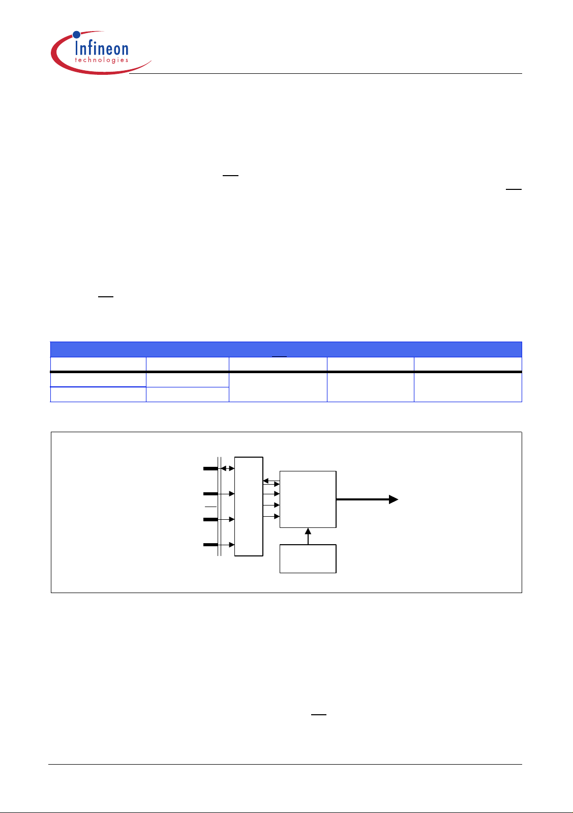
General Description
The IC is a low power consumption single chip FSK/ASK
Transceiver for half duplex low datarate communication in the
868-870MHz band. The IC offers a very high level of integration
and needs only a few external components. It contains a highly
efficient power amplifier, a low noise amplifier (LNA) with AGC,
a double balanced mixer, a complex direct conversion stage, I/
Q limiters with RSSI generation, an FSK demodulator, a fully
integrated VCO and PLL synthesizer, a tuneable crystal
oscillator, an onboard data filter, a data comparator (slicer),
positive and negative peak detectors, a data rate detection
circuit and a 2/3-wire bus interface. Additionally there is a power
down feature to save battery power.
Version 1.7
Features
■ Low supply current (I
Is = 12mA typ. transmit mode)
■ Supply voltage range 2.1 - 5.5V
■ Power down mode with very low supply cur-
rent consumption
■ FSK and ASK modulation and demodula-
tion capability
■ Fully integrated VCO and PLL
synthesizer and loop filter on-chip with on
chip crystal oscillator tuning
2
■ I
C/3-wire µController Interface
= 9mA typ. receive,
s
Application
■ Low Bitrate Communication
Systems
■ Keyless Entry Systems
■ Remote Control Systems
■ On-chip low pass channel select filter and
data filter with tuneable bandwidth
■ Data slicer with self-adjusting threshold and
2 peak detectors
■ FSK sensitivity <-109dBm, ASK sensitivity
< –109dBm
■ Transmit power up to +13dBm
■ Datarates up to 64kBit/s Manchester
encoded
■ Self-polling logic with ultra fast data rate
detection
■ Alarm Systems
■ Telemetry Systems
■ Electronic Metering
■ Home Automation Systems
Type Ordering Code Package
TDA5250 D2 SP000012956 <Dev_Package1>
Data Sheet 5 2007-02-26

TDA5250 D2
Version 1.7
Table of Contents
page
1 Product Description . . . . . . . . . . . . . . . . . . . . . . . . . . . . . . . . . . . . . . . . . . 9
1.1 Overview . . . . . . . . . . . . . . . . . . . . . . . . . . . . . . . . . . . . . . . . . . . . 9
1.2 Features . . . . . . . . . . . . . . . . . . . . . . . . . . . . . . . . . . . . . . . . . . . . . 9
1.3 Application . . . . . . . . . . . . . . . . . . . . . . . . . . . . . . . . . . . . . . . . . . . 10
1.4 Package Outlines . . . . . . . . . . . . . . . . . . . . . . . . . . . . . . . . . . . . . . 10
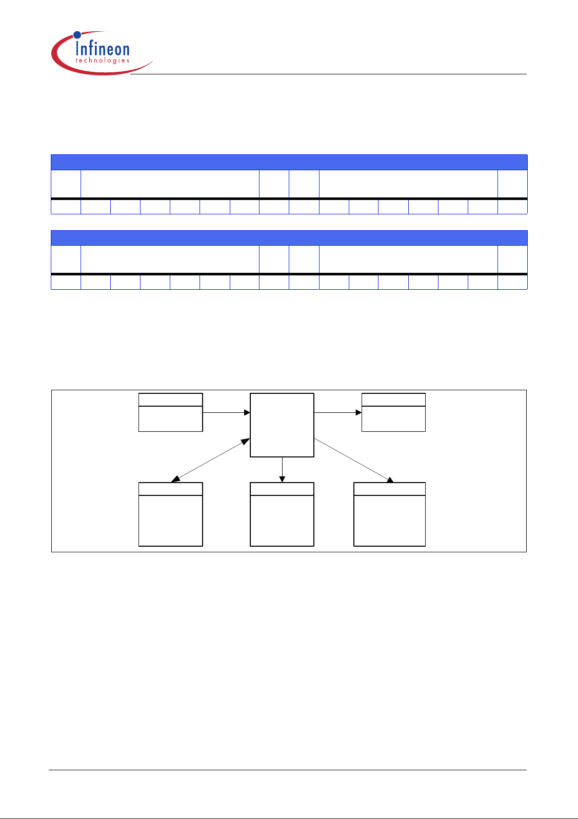
2 Functional Description . . . . . . . . . . . . . . . . . . . . . . . . . . . . . . . . . . . . . . . 11
2.1 Pin Configuration . . . . . . . . . . . . . . . . . . . . . . . . . . . . . . . . . . . . . . 11
2.2 Pin Definitions and Functions . . . . . . . . . . . . . . . . . . . . . . . . . . . . 12
2.3 Functional Block Diagram . . . . . . . . . . . . . . . . . . . . . . . . . . . . . . . 18
2.4 Functional Block Description . . . . . . . . . . . . . . . . . . . . . . . . . . . . . 19
2.4.1 Power Amplifier (PA) . . . . . . . . . . . . . . . . . . . . . . . . . . . . . . . . . 19
2.4.2 Low Noise Amplifier (LNA) . . . . . . . . . . . . . . . . . . . . . . . . . . . . . 19
2.4.3 Downconverter 1st Mixer . . . . . . . . . . . . . . . . . . . . . . . . . . . . . . 19
2.4.4 Downconverter 2nd I/Q Mixers . . . . . . . . . . . . . . . . . . . . . . . . . . 19
2.4.5 PLL Synthesizer . . . . . . . . . . . . . . . . . . . . . . . . . . . . . . . . . . . . . 20
2.4.6 I/Q Filters . . . . . . . . . . . . . . . . . . . . . . . . . . . . . . . . . . . . . . . . . . 20
2.4.7 I/Q Limiters . . . . . . . . . . . . . . . . . . . . . . . . . . . . . . . . . . . . . . . . 20
2.4.8 FSK Demodulator . . . . . . . . . . . . . . . . . . . . . . . . . . . . . . . . . . . 21
2.4.9 Data Filter . . . . . . . . . . . . . . . . . . . . . . . . . . . . . . . . . . . . . . . . . 21
2.4.10 Data Slicer . . . . . . . . . . . . . . . . . . . . . . . . . . . . . . . . . . . . . . . . . 22
2.4.11 Peak Detectors . . . . . . . . . . . . . . . . . . . . . . . . . . . . . . . . . . . . . 22
2.4.12 Crystal Oscillator . . . . . . . . . . . . . . . . . . . . . . . . . . . . . . . . . . . . 22
2.4.13 Bandgap Reference Circuitry & Powerdown . . . . . . . . . . . . . . . 22
2.4.14 Timing and Data Control Unit . . . . . . . . . . . . . . . . . . . . . . . . . . 23
2.4.15 Bus Interface and Register Definition . . . . . . . . . . . . . . . . . . . . 24
2.4.16 Wakeup Logic . . . . . . . . . . . . . . . . . . . . . . . . . . . . . . . . . . . . . . 32
2.4.17 Data Valid Detection, Data Pin . . . . . . . . . . . . . . . . . . . . . . . . . 33
2.4.18 Sequence Timer . . . . . . . . . . . . . . . . . . . . . . . . . . . . . . . . . . . . 34
2.4.19 Clock Divider . . . . . . . . . . . . . . . . . . . . . . . . . . . . . . . . . . . . . . . 36
2.4.20 RSSI and Supply Voltage Measurement . . . . . . . . . . . . . . . . . . 37
3 Application . . . . . . . . . . . . . . . . . . . . . . . . . . . . . . . . . . . . . . . . . . . . . . . . . 39
3.1 LNA and PA Matching . . . . . . . . . . . . . . . . . . . . . . . . . . . . . . . . . . 39
3.1.1 RX/TX Switch . . . . . . . . . . . . . . . . . . . . . . . . . . . . . . . . . . . . . . . 39
3.1.2 . . . . . . . . . . . . . . . . . . . . . . . . . . . . . . . . . . . . . . . . . . . . . . . . . . Switch in
RX-Mode . . . . . . . . . . . . . . . . . . . . . . . . . . . . . . . . . . . . . . . . . . 39
3.1.3 . . . . . . . . . . . . . . . . . . . . . . . . . . . . . . . . . . . . . . . . . . . . . . . . . . Switch in
Data Sheet 6 2007-02-26

TDA5250 D2
Version 1.7
Table of Contents
page
TX-Mode . . . . . . . . . . . . . . . . . . . . . . . . . . . . . . . . . . . . . . . . . . 42
3.1.4 Power-Amplifier . . . . . . . . . . . . . . . . . . . . . . . . . . . . . . . . . . . . . 44
3.2 Crystal Oscillator . . . . . . . . . . . . . . . . . . . . . . . . . . . . . . . . . . . . . . 50
3.2.1 Synthesizer Frequency setting . . . . . . . . . . . . . . . . . . . . . . . . . 53
3.2.2 Transmit/Receive ASK/FSK Frequency Assignment . . . . . . . . . 53
3.2.3 Parasitics . . . . . . . . . . . . . . . . . . . . . . . . . . . . . . . . . . . . . . . . . . 56
3.2.4 Calculation of the external capacitors . . . . . . . . . . . . . . . . . . . . 57
3.2.5 FSK-switch modes . . . . . . . . . . . . . . . . . . . . . . . . . . . . . . . . . . . 57
3.2.6 Finetuning and FSK modulation relevant registers . . . . . . . . . . 58
3.2.7 Chip and System Tolerances . . . . . . . . . . . . . . . . . . . . . . . . . . . 59
3.3 IQ-Filter . . . . . . . . . . . . . . . . . . . . . . . . . . . . . . . . . . . . . . . . . . . . . 60
3.4 Data Filter . . . . . . . . . . . . . . . . . . . . . . . . . . . . . . . . . . . . . . . . . . . 61
3.5 Limiter and RSSI . . . . . . . . . . . . . . . . . . . . . . . . . . . . . . . . . . . . . . 62
3.6 Data Slicer - Slicing Level . . . . . . . . . . . . . . . . . . . . . . . . . . . . . . . 64
3.6.1 RC Integrator . . . . . . . . . . . . . . . . . . . . . . . . . . . . . . . . . . . . . . . 64
3.6.2 Peak Detectors . . . . . . . . . . . . . . . . . . . . . . . . . . . . . . . . . . . . . 65
3.6.3 Peak Detector - Analog output signal . . . . . . . . . . . . . . . . . . . . 67
3.6.4 Peak Detector – Power Down Mode . . . . . . . . . . . . . . . . . . . . . 67
3.7 Data Valid Detection . . . . . . . . . . . . . . . . . . . . . . . . . . . . . . . . . . . 68
3.7.1 Frequency Window for Data Rate Detection . . . . . . . . . . . . . . . 70
3.7.2 RSSI threshold voltage - RF input power . . . . . . . . . . . . . . . . . 71
3.8 Calculation of ON_TIME and OFF_TIME . . . . . . . . . . . . . . . . . . . 71
3.9 Example for Self Polling Mode . . . . . . . . . . . . . . . . . . . . . . . . . . . . 72
3.10 Sensitivity Measurements . . . . . . . . . . . . . . . . . . . . . . . . . . . . . . . 73
3.10.1 Test Setup . . . . . . . . . . . . . . . . . . . . . . . . . . . . . . . . . . . . . . . . . 73
3.10.2 Sensitivity depending on the ambient Temperature . . . . . . . . . 75
3.10.3 BER performance depending on Supply Voltage . . . . . . . . . . . 76
3.10.4 Datarates and Sensitivity . . . . . . . . . . . . . . . . . . . . . . . . . . . . . . 76
3.10.5 Sensitivity at Frequency Offset . . . . . . . . . . . . . . . . . . . . . . . . . 77
3.11 Default Setup . . . . . . . . . . . . . . . . . . . . . . . . . . . . . . . . . . . . . . . . . 78
4 Reference . . . . . . . . . . . . . . . . . . . . . . . . . . . . . . . . . . . . . . . . . . . . . . . . . . 79
4.1 Electrical Data . . . . . . . . . . . . . . . . . . . . . . . . . . . . . . . . . . . . . . . . 79
4.1.1 Absolute Maximum Ratings . . . . . . . . . . . . . . . . . . . . . . . . . . . . 79
4.1.2 Operating Range . . . . . . . . . . . . . . . . . . . . . . . . . . . . . . . . . . . . 79
4.1.3 AC/DC Characteristics . . . . . . . . . . . . . . . . . . . . . . . . . . . . . . . . 80
4.1.4 Digital Characteristics . . . . . . . . . . . . . . . . . . . . . . . . . . . . . . . . 83
Data Sheet 7 2007-02-26

TDA5250 D2
Version 1.7
Table of Contents
page
4.2 Test Circuit . . . . . . . . . . . . . . . . . . . . . . . . . . . . . . . . . . . . . . . . . . . 86
4.3 Test Board Layout . . . . . . . . . . . . . . . . . . . . . . . . . . . . . . . . . . . . . 87
4.4 Bill of Materials . . . . . . . . . . . . . . . . . . . . . . . . . . . . . . . . . . . . . . . 88
Data Sheet 8 2007-02-26

TDA5250 D2
Version 1.7
Product Description
1 Product Description
1.1 Overview
The IC is a low power consumption single chip FSK/ASK Transceiver for the frequency band 868870 MHz. The IC combines a very high level of integration and minimum external part count. The
device contains a low noise amplifier (LNA), a double balanced mixer, a fully integrated VCO, a PLL
synthesizer, a crystal oscillator with FSK modulator, a limiter with RSSI generator, an FSK
demodulator, a data filter, a data comparator (slicer), a positive and a negative data peak detector,
a highly efficient power amplifier and a complex digital timing and control unit with I
microcontroller interface. Additionally there is a power down feature to save battery power.
The transmit section uses direct ASK modulation by switching the power amplifier, and crystal
oscillator detuning for FSK modulation. The necessary detuning load capacitors are external. The
capacitors for fine tuning are integrated. The receive section is using a novel single-conversion/
direct-conversion scheme that is combining the advantages of both receive topologies. The IF is
contained on the chip, no RF channel filters are necessary as the channel filter is also on the chip.
The self-polling logic can be used to let the device operate autonomously as a master for a decoding
microcontroller.
2
C/3-wire
1.2 Features
■ Low supply current (I
voltage, 25°C)
■ Supply voltage range 2.1 V to 5.5 V
■ Operating temperature range -40°C to +85°C
■ Power down mode with very low supply current consumption
■ FSK and ASK modulation and demodulation capability without external circuitry changes, FM
demodulation capability
■ Fully integrated VCO and PLL synthesizer and loop filter on-chip with on-chip crystal oscillator
tuning, therefore no additional external components necessary
■ Differential receive signal path completely on-chip, therefore no external filters are necessary
■ On-chip low pass channel select and data filter with tuneable bandwith
■ Data slicer with self-adjusting threshold and 2 peak detectors
■ Self-polling logic with adjustable duty cycle and ultrafast data rate detection and timer mode
providing periodical interrupt
■ FSK and ASK sensitivity < -109 dBm
■ Adjustable LNA gain
■ Digital RSSI and Battery Voltage Readout
■ Provides Clock Out Pin for external microcontroller
■ Transmit power up to +13 dBm in 50Ω
■ Maximum datarate up to 64 kBaud Manchester encoded
2
■ I
C/3-wire microcontroller interface, working at max. 400kbit/s
■ meets the ETSI EN300 220 regulation and CEPT ERC 7003 recommendation
= 9 mA typ. receive, Is = 12mA typ. transmit mode, both at 3 V supply
s
load at 5V supply voltage
Data Sheet 9 2007-02-26
TDA5250 D2
Version 1.7
1.3 Application
■ Low Bitrate Communication Systems
■ Keyless Entry Systems
■ Remote Control Systems
■ Alarm Systems
■ Telemetry Systems
■ Electronic Metering
■ Home Automation Systems
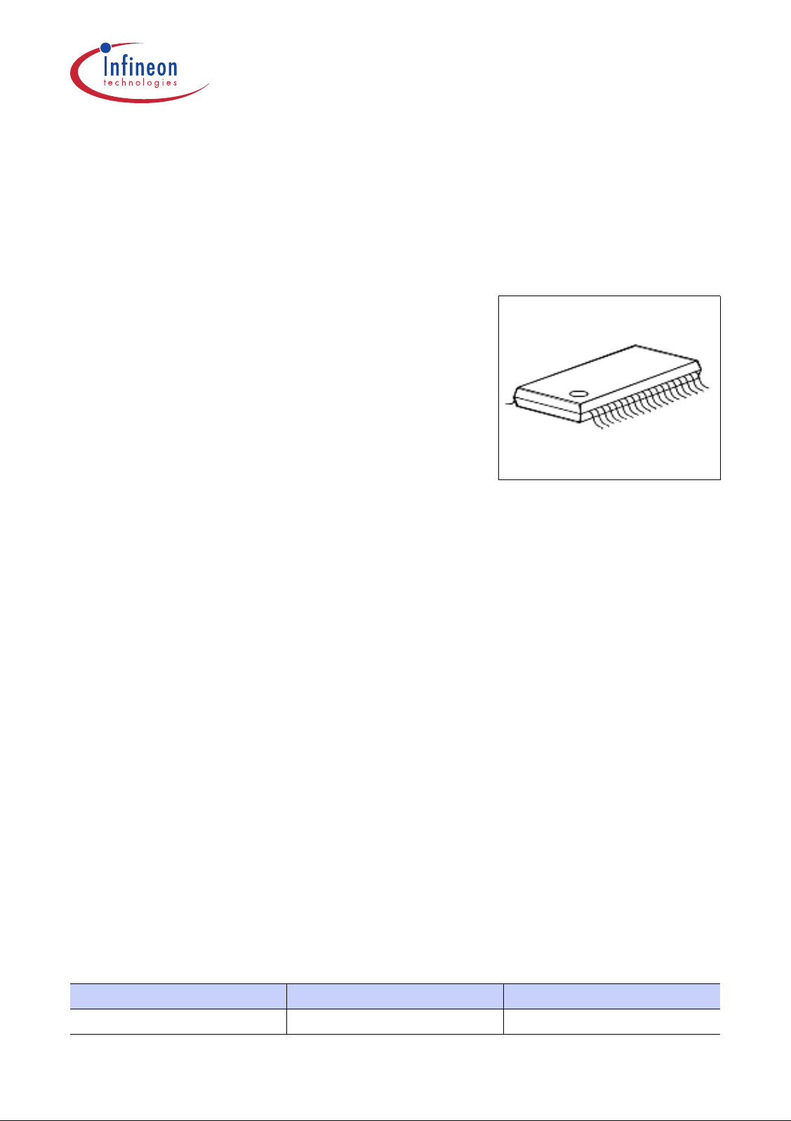
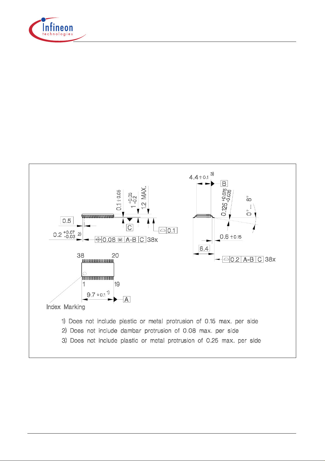
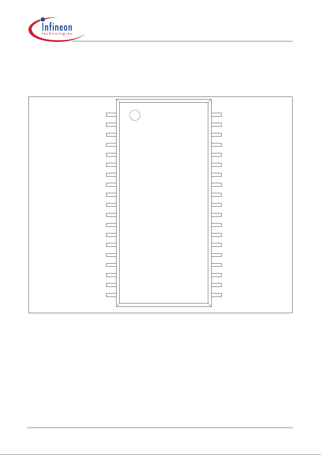
1.4 Package Outlines
Product Description
PG-TSSOP-38.EPS
Figure 1-1 PG-TSSOP-38 package outlines
Data Sheet 10 2007-02-26
TDA5250 D2
Version 1.7
2 Functional Description
2.1 Pin Configuration
VCC
BUSMODE
LF
____
ASKFSK
__
RxTx
LNI
LNIx
GND1
GNDPA
PA
VCC1
PDN
PDP
SLC
VDD
BUSDATA
BUSCLK
VSS
XOUT
10
11
12
13
14
15
16
17
18
19
1
2
3
4
5
6
7
8
9
TDA5250
Functional Description
38
37
36
35
34
33
32
31
30
29
28
27
26
25
24
23
22
21
20
CI1
CI1x
CQ1
CQ1x
CI2
CI2x
CQ2
CQ2x
GND
RSSI
DATA
___
PWDDD
CLKDIV
______
RESET
___
EN
XGND
XSWA
XIN
XSWF
5250D1_pin_conf.wmf
Figure 2-1 Pin Configuration
Data Sheet 11 2007-02-26
TDA5250 D2
Version 1.7
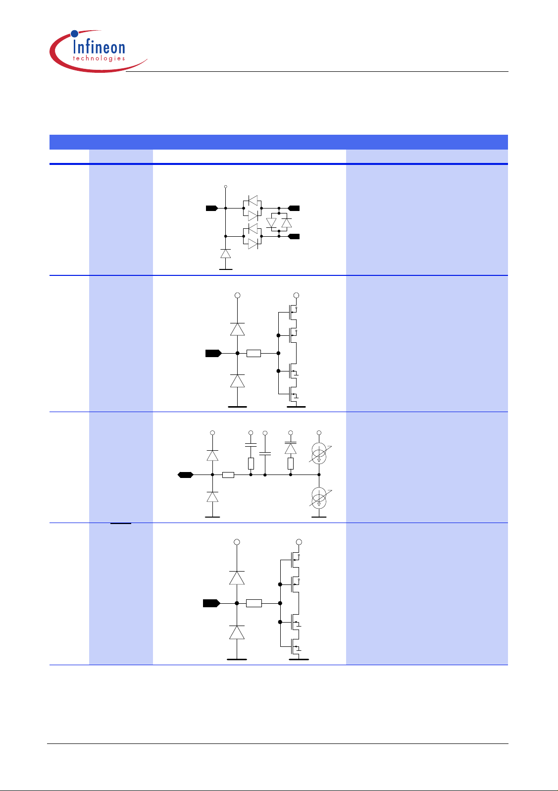
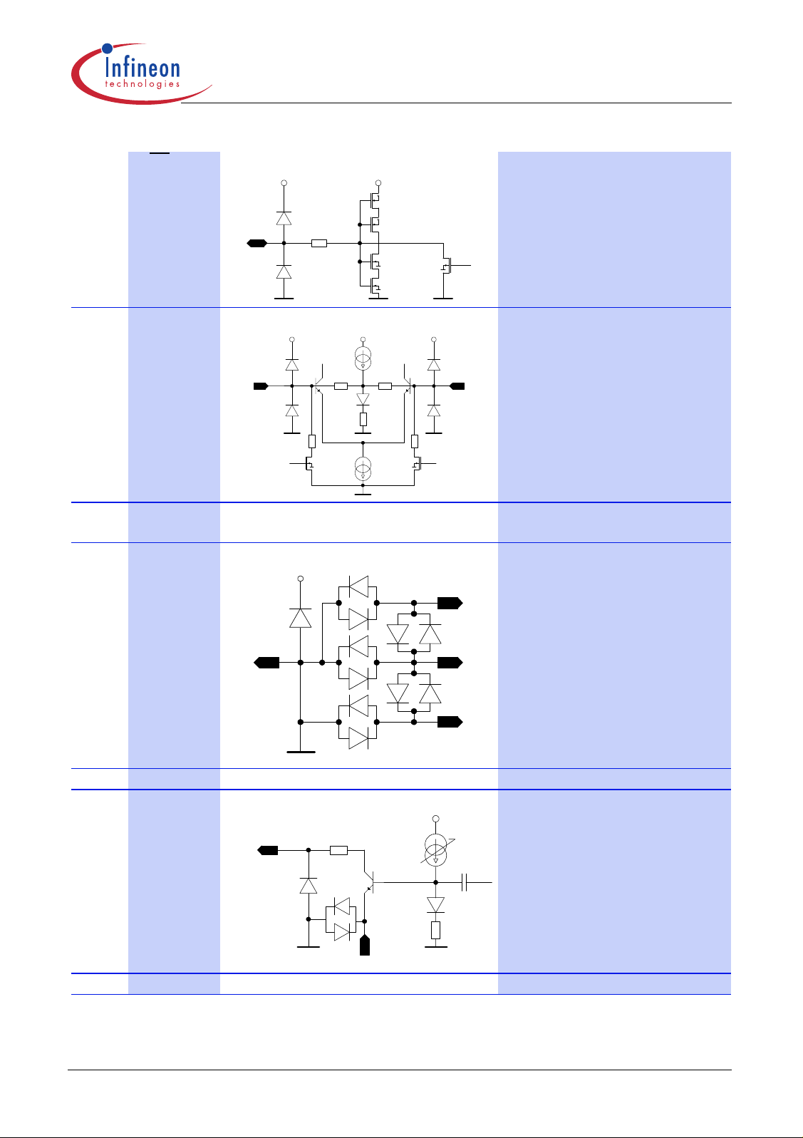
2.2 Pin Definitions and Functions
Table 2-1 Pin Definition and Function
Pin No.
1
2
Symbol Equivalent I/O-Schematic Function
VCC Analog supply (antiparallel diodes
1 11
BUSMODE Bus mode selection (I²C/3 wire bus
350
2
Functional Description
between VCC, VCC1, VDD)
15
mode selection)
3
4
LF Loop filter and VCO control voltage
3
200
ASKFSK ASK/FSK- mode switch input
4
350
Data Sheet 12 2007-02-26
TDA5250 D2
Version 1.7
Functional Description
5 RXTX RX/TX-mode switch input/output
5
6
LNI RF input to differential Low Noise
350
TX
Amplifier (LNA))
5k 5k
6
PWDN
7
VCC see Pin 6 Analog supply (antiparallel diodes
1.1V
7
180180
PWDN
between VCC, VCC1, VDD
8
BUSMODE Bus mode selection (I²C/3 wire bus
mode selection)
9
10
11
30
8
18
9
GNDPA see Pin 8 Ground return for PA output stage
PA PA output stage
10
10
Ω
9
GndPA
VCC1 see Pin 1 Supply for LNA and PA
Data Sheet 13 2007-02-26
TDA5250 D2
Version 1.7
Functional Description
12 PDN Output of the negative peak
detector
13
14
PWDN
12
350
50k
3k
PDP Output of the positive peakdetector
50k
13
350
3k
PWDN
SLC Slicer level for the data slicer
1.2uA
14
350
50k
50k 50k
50k
50k
50k
15
16
17
1.2uA
50k 50k
VDD see Pin 1 Digital supply
BUSDATA Bus data in/output
15k
16
350
BUSCLK Bus clock input
17
350
18
VSS see Pin 8 Ground for digital section
Data Sheet 14 2007-02-26
TDA5250 D2
Version 1.7
Functional Description
19 XOUT Crystal oscillator output, can also
be used as external reference
frequency input.
4k
Vcc
20
Vcc-860mV
µ
A
150
XSWF FSK modulation switch
125fF ..... 4pF
250fF ..... 8pF
19
21
20
23
21
XIN see Pin 20
22 XSWA ASK modulation/FSK center
frequency switch
22
20
23
23
24
XGND
see Pin 22
Crystal oscillator ground return
EN 3-wire bus enable input
24
350
Data Sheet 15 2007-02-26
TDA5250 D2
Version 1.7
Functional Description
25 RESET Reset of the entire system (to
default values), active low
110k
350
10p
350
26
25
CLKDIV Clock output
26
27
28
29
PWDDD Power Down input (active high),
data detect output (active low)
30k
27
350
DATA TX Data input, RX data output (RX
powerdown: pin 28 @ GND)
28
350
RSSI RSSI output
29
350
37k
16p
S&H
Data Sheet 16 2007-02-26
TDA5250 D2
Version 1.7
Functional Description
30 GND see Pin 8 Analog ground
31
CQ2x Pin for external Capacitor
Q-channel, stage 2
Stage1:Vcc-630mV
Stage2: Vcc-560mV
32
33
34
35
36
37
38
31
CQ2 II Q-channel, stage 2
CI2x II I-channel, stage 2
CI2 II I-channel, stage 2
CQ1x II Q-channel, stage 1
CQ1 II Q-channel, stage 1
CI1x II I-channel, stage 1
CI1 II I-channel, stage 1
Data Sheet 17 2007-02-26
TDA5250 D2
Version 1.7
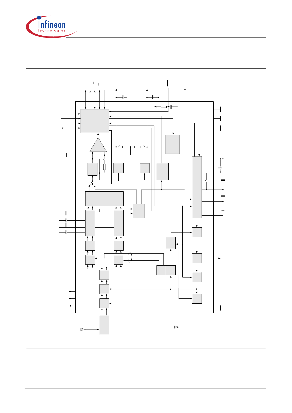
2.3 Functional Block Diagram
PDP
ASKFSK
13
4
100k
100k
-
ASK/FSK
100k
Det
+Peak
BUSMODE
__
EN
BUSCLK
BUSDATA
RXTX
Data (RX/TX)
CLKDIV
PWDDD
5
282627
LOGIC
17 24 2
16
SLC
14
WAKEUP
INTERFACE
CONTROLLER
SLICER
+
Data
FILTER
ASK
FSK
Functional Description
PDN
12
Det
-Peak
RESET
VCC
25
6-bit
SAR-ADC
Bandgap
Reference
RSSI
29
18
(digital)
(analog)
(LNA/PA)
FSK DATA
CLK
VssGnd1
30
Gnd
8
XSWA XGND
22 23
20
XSWF
QUADRI
CORRELATOR
CQ2x
31
32
CQ2
33
CI2x
34
CI2
CQ1x
35
36
CQ1
CI1x
CI1
(digital)
15
1
(analog)
(LNA/PA)
11
LIMITE R
I
Filter
Channel
MIXER
LP
= 289.433MHz
IF
f
6
LNI
= 868.3MHz
RF
f
ANT
37
38
VDD
VCC
VCC1
single ended to
LIMITE R
Filter
Q
Channel
MIXER
FILTER
LNA MIXER
high/low
7
LNIx
differential conv.
Gain
RSSI
0°
90°
f = 289.433MHz
ASK/FSK
TX/RX
ASK DATA
PHASE
:12/16
TX/RX
:4
10
PA
ANT
CRYSTAL Osc, FSKMod, Finetuning
DET.
LOOP
VCO
PA
21
= 18.0896MHz
Q
f
XOUT
19
Charge P.
39
FILTER
= 868.3MHz
TX
f
LF
= 1157.73MHz
RX
f
GndPA
XIN
TDA5250D1_blockdiagram_aktuell.wmf
Figure 2-2 Main Block Diagram
Data Sheet 18 2007-02-26
TDA5250 D2
Version 1.7
Functional Description
2.4 Functional Block Description
2.4.1 Power Amplifier (PA)
The power amplifier is operating in C-mode. It can be used in either high or low power mode. In
high-power mode the transmit power is approximately +13dBm into 50 Ohm at 5V and +4dBm at
2.1V supply voltage. In low power mode the transmit power is approximately -7dBm at 5V and 32dBm at 2.1V supply voltage using the same matching network. The transmit power is controlled
by the D0-bit of the CONFIG register (subaddress 00H) as shown in the following Table 2-2. The
default output power mode is high power mode.
Table 2-2 Sub Address 00H: CONFIG
Bit
D0
In case of ASK modulation the power amplifier is turned fully on and off by the transmit baseband
data, i.e. 100% On-Off-Keying.
Function Description Default
PA_PWR 0= low TX Power, 1= high TX Power 1
2.4.2 Low Noise Amplifier (LNA)
The LNA is an on-chip cascode amplifier with a voltage gain of 15 to 20dB and symmetrical inputs.
It is possible to reduce the gain to 0 dB via logic.
Table 2-3 Sub Address 00H: CONFIG
Bit
D4
Function Description Default
LNA_GAIN 0= low Gain, 1= high Gain 1
2.4.3 Downconverter 1st Mixer
The Double Balanced 1st Mixer converts the input frequency (RF) in the range of 868-870 MHz
down to the intermediate frequency (IF) at approximately 290MHz. The local oscillator frequency is
generated by the PLL synthesizer that is fully implemented on-chip as described in Section 2.4.5.
This local oscillator operates at approximately 1157MHz in receive mode providing the above
mentioned IF frequency of 290MHz. The mixer is followed by a low pass filter with a corner
frequency of approximately 350MHz in order to prevent RF and LO signals from appearing in the
290MHz IF signal.
2.4.4 Downconverter 2nd I/Q Mixers
The Low pass filter is followed by 2 mixers (inphase I and quadrature Q) that convert the 289MHz
IF signal down to zero-IF. These two mixers are driven by a signal that is generated by dividing the
local oscillator signal by 4, thus equalling the IF frequency.
Data Sheet 19 2007-02-26
TDA5250 D2
Version 1.7
Functional Description
2.4.5 PLL Synthesizer
The Phase Locked Loop synthesizer consists of two VCOs (i.e. transmit and receive VCO), a
divider by 4, an asynchronous divider chain with selectable overall division ratio, a phase detector
with charge pump and a loop filter and is fully implemented on-chip. The VCOs are including spiral
inductors and varactor diodes. The center frequency of the transmit VCO is 868MHz, the center
frequency of the receive VCO is 1156MHz.
Generally in receive mode the relationship between local oscillator frequency f
frequency fRF and the IF frequency fIF and thus the frequency that is applied to the I/Q Mixers is
given in the following formula:
f
= 4/3 fRF = 4 f
osc
The VCO signal is applied to a divider by 4 which is producing approximately 289MHz signals in
quadrature. The overall division ratio of the divider chain following the divider by 4 is 12 in transmit
mode and 16 in receive mode as the nominal crystal oscillator frequency is 18.083MHz. The
division ratio is controlled by the RxTx
IF
pin (pin 5) and the D10 bit in the CONFIG register.
[2 – 1]
, the receive RF
osc
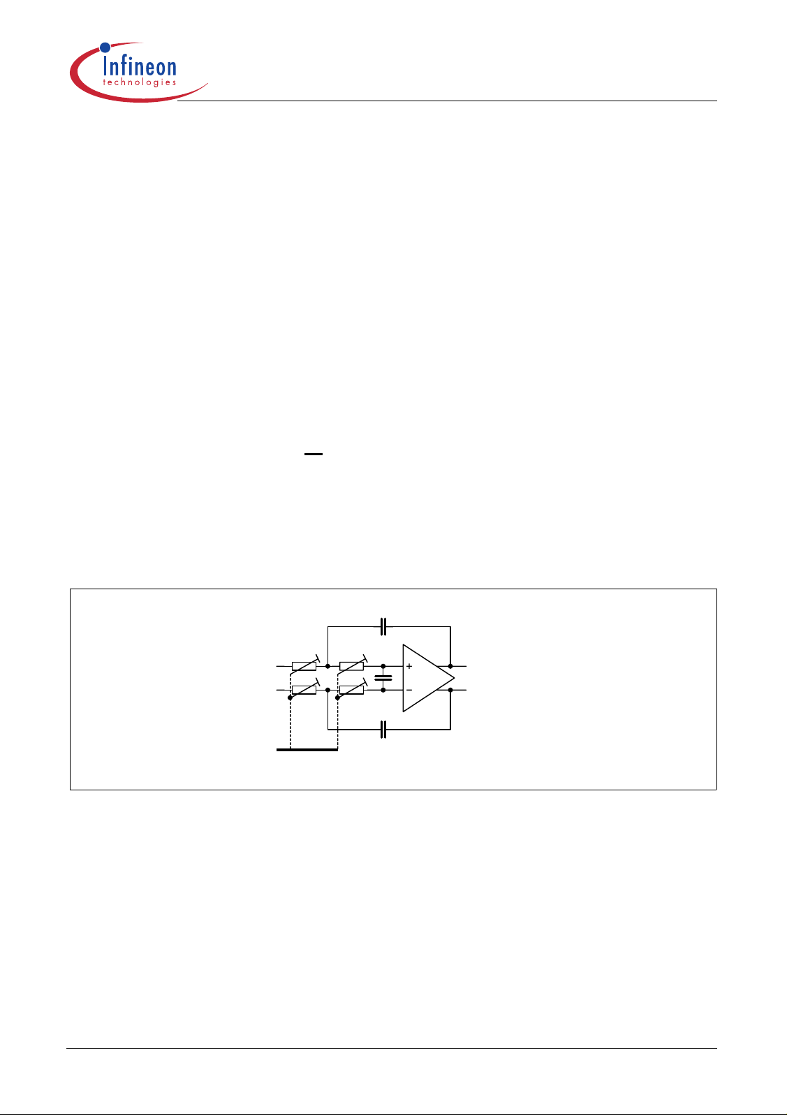
2.4.6 I/Q Filters
The I/Q IF to zero-IF mixers are followed by baseband 6th order low pass filters that are used for
RF-channel filtering.
OP
INTERNAL BUS
iq_filter.wmf
Figure 2-3 One I/Q Filter stage
The bandwidth of the filters is controlled by the values set in the filter-register. It can be adjusted
between 50 and 350kHz in 50kHz steps via the bits D1 to D3 of the LPF register (subaddress 03H).
2.4.7 I/Q Limiters
The I/Q Limiters are DC coupled multistage amplifiers with offset-compensating feedback circuit
and an overall gain of approximately 80dB each in the frequency range of 100Hz up to 350kHz.
Receive Signal Strength Indicator (RSSI) generators are included in both limiters which produce DC
voltages that are directly proportional to the input signal level in the respective channels. The
resulting I- and Q-channel RSSI-signals are summed to the nominal RSSI signal.
Data Sheet 20 2007-02-26
TDA5250 D2
Version 1.7
Functional Description
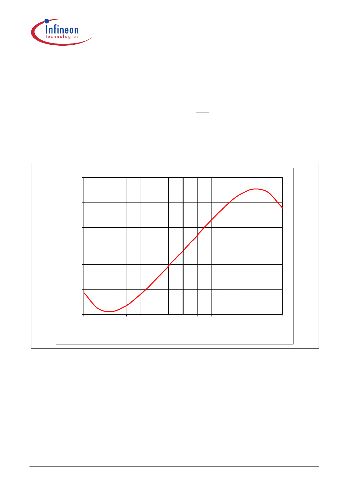
2.4.8 FSK Demodulator
The output differential signals of the I/Q limiters are fed to a quadrature correlator circuit that is used
to demodulate frequency shift keyed (FSK) signals. The demodulator gain is 2.4mV/kHz, the
maximum frequency deviation is ±300kHz as shown in Figure 2-4 below.
The demodulated signal is applied to the ASK/FSK mode switch which is connected to the input of
the data filter. The switch can be controlled by the ASKFSK
CONFIG register.
The modulation index m must be significantly larger than 2 and the deviation at least larger than
25kHz for correct demodulation of the signal.
1,6
1,5
1,4
1,3
1,2
pin (pin 4) and via the D11 bit in the
1,1
U /V
1
0,9
0,8
0,7
0,6
0,5
-350 -300 -250 -200 -150 -100 -50 0 50 100 150 200 250 300 350
f /kHz
Qaudricorrelator.wmf
Figure 2-4 Quadricorrelator Demodulation Characteristic
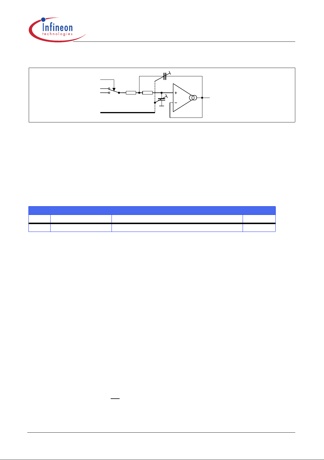
2.4.9 Data Filter
The 2-pole data filter has a Sallen-Key architecture and is implemented fully on-chip. The bandwidth
can be adjusted between approximately 5kHz and 102kHz via the bits D4 to D7 of the LPF register
as shown in Table 3-10.
Data Sheet 21 2007-02-26
TDA5250 D2
Version 1.7
ASK / FSK
OTA
INTER NAL B US
Figure 2-5 Data Filter architecture
Functional Description
data_filter.wmf
2.4.10 Data Slicer
The data slicer is a fast comparator with a bandwidth of 100kHz. The self-adjusting threshold is
generated by a RC-network (LPF) or by use of one or both peak detectors depending on the
baseband coding scheme as described in Section 3.6. This can be controlled by the D15 bit of the
CONFIG register as shown in the following table.
Table 2-4 Sub Address 00H: CONFIG
Bit
D15
Function Description Default
SLICER 0= Lowpass Filter, 1= Peak Detector 0
2.4.11 Peak Detectors
Two separate Peak Detectors are available. They are generating DC voltages in a fast-attack and
slow-release manner that are proportional to the positive and negative peak voltages appearing in
the data signal. These voltages may be used to generate a threshold voltage for non-Manchester
encoded signals, for example. The time-constant of the fast-attack/slow-release action is
determined by the RC network with external capacitor.
2.4.12 Crystal Oscillator
The reference oscillator is an NIC oscillator type (Negative Impedance Converter) with a crystal
operating in serial resonance. The nominal operating frequency of 18.083MHz and the frequencies
for FSK modulation can be adjusted via 3 external capacitors. Via microcontroller and bus interface
the chip-internal capacitors can be used for finetuning of the nominal and the FSK modulation
frequencies. This finetuning of the crystal oscillator allows to eliminate frequency errors due to
crystal or component tolerances.
2.4.13 Bandgap Reference Circuitry & Powerdown
A Bandgap Reference Circuit provides a temperature stable 1.2V reference voltage for the device.
A power down mode is available to switch off all subcircuits that are controlled by the bidirectional
Powerdown&DataDetect PwdDD
can either be activated by pin 27 or bit D14 in register 00h. In powerdown mode also pin 28 (DATA)
is affected (see Section 2.4.17).
pin (pin 27) as shown in the following table. Powerdown mode
Data Sheet 22 2007-02-26
TDA5250 D2
Version 1.7
Functional Description
Table 2-5 PwdDD Pin Operating States
PwdDD
Ground/VSS
Operating State
VDD
Powerdown Mode
Device On
2.4.14 Timing and Data Control Unit
The timing and data control unit contains a wake-up logic unit, an I2C/3-wire microcontroller
interface, a “data valid” detection unit and a set of configuration registers as shown in the
subsequent figure.
BusData
BusCLK
EN
BusMode
I2C / 3Wire
INTERFACE
18 MHz
XTAL-Osz.
INTERNAL BUS
REGISTERS
RF - BLOCK
RSSI
RX DATA
FSK DATA
ASK DATA
BLOCK ENABLE
ASK / FSK
RX / TX
6 Bit
ADC
DATA VALID
DETECTOR
AMPLITUDE
threshold TH3
FREQUENCY
window
TH1<T
GATE
ENABLE
<TH2
DATA
CONTROL
LOGIC
POWER ON
SEQUENCER
VALID
WAKEUP
LOGIC
32kHz
RC-Osz.
CLKDiv
PwdDD
Data
AskFsk
RxTx
Reset
logic.wmf
Figure 2-6 Timing and Data Control Unit
2
The I
C / 3-wire Bus Interface gives an external microcontroller full control over important system
parameters at any time.
It is possible to set the device in three different modes: Slave Mode, Self Polling Mode and Timer
Mode. This is done by a state machine which is implemented in the WAKEUP LOGIC unit. A
detailed description is given in Section 2.4.16.
Data Sheet 23 2007-02-26
TDA5250 D2
Version 1.7
Functional Description
The DATA VALID DETECTOR contains a frequency window counter and an RSSI threshold
comparator. The window counter uses the incoming data signal from the data slicer as the gating
signal and the crystal oscillator frequency as the timebase to determine the actual datarate. The
result is compared with the expected datarate.
The threshold comparator compares the actual RSSI level with the expected RSSI level.
If both conditions are true the PwdDD
pin is set to LOW in self polling mode as you can see in
Section 2.4.16. This signal can be used as an interrupt for an external µP. Because the PwdDD
pin is bidirectional and open drain driven by an internal pull-up resistor it is possible to apply an
external LOW thus enabling the device.
2.4.15 Bus Interface and Register Definition
The TDA5250 supports the I2C bus protocol (2 wire) and a 3-wire bus protocol. Operation is
selectable by the BusMode pin (pin 2) as shown in the following table. All bus pins (BusData,
BusCLK, EN
where the output is open drain driven by an internal 15k
Table 2-6 Bus Interface Format
Function
2
I
3-wire Mode
, BusMode) have a Schmitt-triggered input stage. The BusData pin is bidirectional
Ω pull up resistor.
BusMode EN BusCLK BusData
C Mode Low High= inactive,
High
Low= active
Clock input Data in/out
BusData
16
BusCLK
17
EN
24
BusMode
I2C / 3-wire
INTERFACE
FRONTEND
2
1 1 1 0 0 0 0 0
CHIP ADDRESS
INTERNAL BUS
i2c_3w_bus.wmf
Figure 2-7 Bus Interface
Note: The Interface is able to access the internal registers at any time, even in POWER DOWN
mode. There is no internal clock necessary for Interface operation.
I2C Bus Mode
In this mode the BusMode pin (pin 2) = LOW and the EN pin (pin 24) = LOW.
Data Sheet 24 2007-02-26

TDA5250 D2
Version 1.7
Data Transition:
Data transition on the pin BusData can only occur when BusCLK is LOW. BusData transitions while
BusCLK is HIGH will be interpreted as start or stop condition.
Start Condition (STA):
A start condition is defined by a HIGH to LOW transition of the BusData line while BusCLK is HIGH.
This start condition must precede any command and initiate a data transfer onto the bus.
Stop Condition (STO):
A stop condition is defined by a LOW to HIGH transition of the BusData line while BusCLK is HIGH.
This condition terminates the communication between the devices and forces the bus interface into
the initial state.
Acknowledge (ACK):
Indicates a successful data transfer. The transmitter will release the bus after sending 8 bit of data.
During the 9th clock cycle the receiver will set the SDA line to LOW level to indicate it has received
the 8 bits of data correctly.
Functional Description
Data Transfer Write Mode:
To start the communication, the bus master must initiate a start condition (STA), followed by the 8bit
chip address. The chip address for the TDA5250 is fixed as „1110000“ (MSB at first). The last bit
(LSB=A0) of the chip address byte defines the type of operation to be performed:
A0=0, a write operation is selected and A0=1 a read operation is selected.
After this comparison the TDA5250 will generate an ACK and awaits the desired sub address byte
(00H...0FH) and data bytes. At the end of the data transition the master has to generate the stop
condition (STO).
Data Transfer Read Mode:
To start the communication in the read mode, the bus master must initiate a start condition (STA),
followed by the 8 bit chip address (write: A0=0), followed by the sub address to read (80H, 81H),
followed by the chip address (read: A0=1). After that procedure the data of the selected register
(80H, 81H) is read out. During this time the data line has to be kept in HIGH state and the chip sends
out the data. At the end of data transition the master has to generate the stop condition (STO).
Bus Data Format in I2C Mode
Table 2-7 Chip address Organization
MSB
1 1 1 0 0 0 0 0 Chip Address Write
1 1 1 0 0 0 0 1 Chip Address Read
LSB Function
Data Sheet 25 2007-02-26
TDA5250 D2
Version 1.7
Functional Description
Table 2-8 I2C Bus Write Mode 8 Bit
MSB CHIP ADDRESS
(WRITE)
STA 1 1 1 0 0 0 0 0 ACK S7 S6 S5 S4 S3 S2 S1 S0 ACK D7 D6 D5 D4 D3 D2 D1 D0 ACK STO
LSB MSB SUB ADDRESS (WRITE)
00H...08H, 0DH, 0EH, 0FH
LSB MSB DATA IN LSB
Table 2-9 I2C Bus Write Mode 16 Bit
MSB CHIP ADDRESS (WRITE) LSB MSB SUB ADDRESS (WRITE)
00H...08H, 0DH, 0EH, 0FH
STA 1 1 1 0 0 0 0 0 ACK S7 S6 S5 S4 S3 S2 S1 S0 ACK D15 ... D8 ACK D7 D6 ... D0 ACK STO
LSB MSB DATA IN LSB
Table 2-10 I2C Bus Read Mode
MSB CHIP ADDRESS (WRITE) LSB MSB SUB ADDRESS (READ)
80H, 81H
STA 1 1 1 0 0 0 0 0 ACK S7 S6 S5 S4 S3 S2 S1 S0 ACK STA 1 1 1 0 0 0 0 1 ACK
LSB MSB CHIP ADDRESS (READ) LSB
Table 2-10 I2C Bus Read Mode (continued)
MSB DATA OUT FROM SUB ADDRESS LSB
R7 R6 R5 R4 R3 R2 R1 R0 ACK* STO
* mandatory HIGH
3-wire Bus Mode
In this mode pin 2 (BusMode)= HIGH and Pin 16 (BusData) is in the data input/output pin. Pin 24
(EN
) is used to activate the bus interface to allow the transfer of data to / from the device. When pin
24 (EN
Data Transition:
Data transition on pin 16 (BusData) can only occur if the clock BusCLK is LOW. To perform a data
transfer the interface has to be enabled. This is done by setting the EN
is done via BusData, BusCLK and EN
Data Transfer Write Mode:
To start the communication the EN
data bytes have to follow. The subaddress (00H...0FH) determines which of the data bytes are
transmitted. At the end of data transition the EN
Data transfer Read Mode:
To start the communication in the read mode, the EN
address to read (80H, 81H). Afterwards the device is ready to read out data. At the end of data
transition EN
) is inactive (HIGH), data transfer is inhibited.
line to LOW. A serial transfer
. The bit stream needs no chip address.
line has to be set to LOW. The desired sub address byte and
must be HIGH.
line has to be set to LOW followed by the sub
must be HIGH.
Data Sheet 26 2007-02-26
TDA5250 D2
Version 1.7
Functional Description
Bus Data Format 3-wire Bus Mode
Table 2-11 3-wire Bus Write Mode
MSB
SUB ADDRESS (WRITE)
LSB MSB DATA IN X...0 (X=7 or 15) LSB
00H...08H, 0DH, 0EH,0FH
S7 S6 S5 S4 S3 S2 S1 S0 DX ... D5 D4 D3 D2 D1 D0
Table 2-12 3-wire Bus Read Mode
MSB
SUB ADDRESS (READ)
80H, 81H
LSB MSB DATA OUT FROM
SUB ADDRESS
S7 S6 S5 S4 S3 S2 S1 S0 R7 R6 R5 R4 R3 R2 R1 R0
Register Definition
Sub Addresses Overview
LSB
ADC
RSSI [8 Bit]
CONTROL
CONFIG [16 Bit]
STATUS [8 Bit]
CLK_DIV [8 Bit]
BLOCK_PD [16Bit]
ON_TIME [16 Bi t]
OFF_TIME [16 Bit]
COUNT_TH1 [16Bit]
COUNT_TH2 [16Bit]
RSSI_TH3 [8 Bit]
Figure 2-8 Sub Addresses Overview
I2C - SPI
INTERFACE
WAKEUP
FILTER
LPF [8 Bit]
XTAL
XTAL_TUNE [16Bit]
FSK [16Bit]
XTAL_CONFIG [8 Bit]
register_overview.wmf
Data Sheet 27 2007-02-26

TDA5250 D2
Version 1.7
Functional Description
Subaddress Organization
Table 2-13 Sub Addresses of Data Registers Write
MSB LSB HEX Function Description Bit Length
0
0 0 000 0 000h CONFIG General definition of status bits 16
0 0 000 0 101h FSK Values for FSK-shift 16
0
0
0 0 000 1 002h XTAL_TUNING Nominal frequency 16
0 0 000 1 103h LPF I/Q and data filter cutoff frequencies 8
0
0
0 0 001 0 004h ON_TIME ON time of wakeup counter 16
0 0 001 0 105h OFF_TIME OFF time of wakeup counter 16
0
0
0 0 001 1 006h COUNT_TH1 Lower threshold of window counter 16
0 0 001 1 107h COUNT_TH2 Higher threshold of window counter 16
0
0
0 0 010 0 008h RSSI_TH3 Threshold for RSSI signal 8
0 0 011 0 10Dh CLK_DIV Configuration and Ratio of clock divider 8
0
0
0 0 011 1 00Eh XTAL_CONFIG XTAL configuration 8
0 0 011 1 10Fh BLOCK_PD Building Blocks Power Down 16
0
Table 2-14 Sub Addresses of Data Registers Read
MSB LSB HEX Function Description Bit Length
1
0 0 000 0 080h STATUS Results of comparison: ADC & WINDOW 8
0 0 000 0 181h ADC ADC data out 8
1
Data Byte Specification
Table 2-15 Sub Address 00H: CONFIG
Bit Function Description Default
D15
D14
D13
D12
D11
D10
D9
D8
D7
D6
D5
D4
D3
D2
D1
D0
SLICER 0= Lowpass, 1= Peak Detector 0
ALL_PD 0= normal operation, 1= all Power down 0
TESTMODE 0= normal operation, 1=Testmode 0
CONTROL 0= RX/TX and ASK/FSK external controlled, 1= Register
controlled
ASK_NFSK 0= FSK, 1=ASK 0
RX_NTX 0= TX, 1=RX 1
CLK_EN 0= CLK off during power down, 1= always CLK on, ever in PD 0
RX_DATA_INV 0= no Data inversion, 1= Data inversion 0
D_OUT 0= Data out if valid, 1= always Data out 1
ADC_MODE 0= one shot, 1= continuous 1
F_COUNT_MODE 0= one shot, 1= continuous 1
LNA_GAIN 0= low gain, 1= high gain 1
EN_RX 0= disable receiver, 1= enable receiver (in self polling and
timer mode) *
MODE_2 0= slave mode, 1= timer mode 0
MODE_1 0= slave or timer mode, 1= self polling mode 0
PA_PWR 0= low TX Power, 1= high TX Power 1
0
1
Note D3: Function is only active in selfpolling and timer mode. When D3 is set to LOW the RX path
is not enabled if PwdDD
pin is set to LOW. A delayed setting of D3 results in a delayed power ON
of the RX building blocks.
Data Sheet 28 2007-02-26
TDA5250 D2
Version 1.7
Functional Description
Subaddress Organization
Table 2-16 Sub Addresses of Data Registers Write
MSB LSB HEX Function Description Bit Length
0
0 0 000 0 000h CONFIG General definition of status bits 16
0 0 000 0 101h FSK Values for FSK-shift 16
0
0
0 0 000 1 002h XTAL_TUNING Nominal frequency 16
0 0 000 1 103h LPF I/Q and data filter cutoff frequencies 8
0
0
0 0 001 0 004h ON_TIME ON time of wakeup counter 16
0 0 001 0 105h OFF_TIME OFF time of wakeup counter 16
0
0
0 0 001 1 006h COUNT_TH1 Lower threshold of window counter 16
0 0 001 1 107h COUNT_TH2 Higher threshold of window counter 16
0
0
0 0 010 0 008h RSSI_TH3 Threshold for RSSI signal 8
0 0 011 0 10Dh CLK_DIV Configuration and Ratio of clock divider 8
0
0
0 0 011 1 00Eh XTAL_CONFIG XTAL configuration 8
0 0 011 1 10Fh BLOCK_PD Building Blocks Power Down 16
0
Table 2-17 Sub Addresses of Data Registers Read
MSB LSB HEX Function Description Bit Length
0 0 000 0 0 80h STATUS Results of comparison: ADC & WINDOW 8
1
0 0 000 0 1 81h ADC ADC data out 8
1
Data Byte Specification
Table 2-18 Sub Address 00H: CONFIG
Bit Function Description Default
D15
D14
D13
D12
D11
D10
D9
D8
D7
D6
D5
D4
D3
D2
D1
D0
Note D3: Function is only active in selfpolling and timer mode. When D3 is set to LOW the RX path
is not enabled if PwdDD
of the RX building blocks.
SLICER 0= Lowpass, 1= Peak Detector 0
ALL_PD 0= normal operation, 1= all Power down 0
TESTMODE 0= normal operation, 1=Testmode 0
CONTROL 0= RX/TX and ASK/FSK external controlled, 1= Register controlled 0
ASK_NFSK 0= FSK, 1=ASK 0
RX_NTX 0= TX, 1=RX 1
CLK_EN 0= CLK off during power down, 1= always CLK on, ever in PD 0
RX_DATA_INV 0= no Data inversion, 1= Data inversion 0
D_OUT 0= Data out if valid, 1= always Data out 1
ADC_MODE 0= one shot, 1= continuous 1
F_COUNT_MODE 0= one shot, 1= continuous 1
LNA_GAIN 0= low gain, 1= high gain 1
EN_RX 0= disable receiver, 1= enable receiver (in self polling and timer mode) * 1
MODE_2 0= slave mode, 1= timer mode 0
MODE_1 0= slave or timer mode, 1= self polling mode 0
PA_PWR 0= low TX Power, 1= high TX Power 1
pin is set to LOW. A delayed setting of D3 results in a delayed power ON
Data Sheet 29 2007-02-26

TDA5250 D2
Version 1.7
Table 2-19 Sub Address 01H: FSK
Bit Function Value Description Default
D15 not used 0
D14 not used 0
D13 FSK+5 8pF Setting for
D12 FSK+4 4pF 0
D11 FSK+3 2pF 1
D10 FSK+2 1pF 0
D9 FSK+1 500fF 1
D8 FSK+0 250fF 0
D7 not used 0
D6 not used 0
D5 FSK-5 4pF Setting for
D4 FSK-4 2pF 0
D3 FSK-3 1pF 1
D2 FSK-2 500fF 1
D1 FSK-1 250fF 0
D0 FSK-0 125fF 0
Table 2-21 Sub Address 03H: LPF
Bit Function Description Default
D7
D6
D5
D4
D3
D2
D1
D0
Datafilter_3
Datafilter_2 0
Datafilter_1 0
Datafilter_0 1
IQ_Filter_2 3dB cutoff
IQ_Filter_1 0
IQ_Filter_0 0
not used 0
positive
frequency
shift: +FSK or
ASK-RX
negative
frequency
shift: -FSK
3dB cutoff
frequency of
data filter
frequency of
IQ-filter
Functional Description
Table 2-20 Sub Address 02H: XTAL_TUNING
Bit Function Value Description Default
D15 not used 0
0
0
0
1
D14 not used 0
D13 not used 0
D12 not used 0
D11 not used 0
D10 not used 0
D9 not used 0
D8 not used 0
D7 not used 0
D6 not used 0
D5 Nominal_Frequ_5 8pF Setting for
D4 Nominal_Frequ_4 4pF 1
D3 Nominal_Frequ_3 2pF 0
D2 Nominal_Frequ_2 1pF 0
D1 Nominal_Frequ_1 500fF 1
D0 Nominal_Frequ_0 250fF 0
Table 2-22 Sub Addresses 04H / 05H: ON/OFF_TIME
Bit
D15
D14
D13
D12
D11
D10
D9
D8
D7
D6
D5
D4
D3
D2
D1
D0
Function Default ON_TIME Default
ON_15 / OFF_15 1 1
ON_14 / OFF_14 1 1
ON_13 / OFF_13 1 1
ON_12 / OFF_12 1 1
ON_11 / OFF_11 1 0
ON_10 / OFF_10 1 0
ON_9 / OFF_9 1 1
ON_8 / OFF_8 0 1
ON_7 / OFF_7 1 1
ON_6 / OFF_6 1 0
ON_5 / OFF_5 0 0
ON_4 / OFF_4 0 0
ON_3 / OFF_3 0 0
ON_2 / OFF_2 0 0
ON_1 / OFF_1 0 0
ON_0 / OFF_0 0 0
nominal
frequency
ASK-TX
FSK-RX
OFF_TIME
0
Table 2-23 Sub Address 06H: COUNT_TH1
Bit
D15
D14
D13
D12
D11
D10
D9
D8
D7
D6
D5
D4
D3
D2
D1
D0
Function Default
not used 0
not used 0
not used 0
not used 0
TH1_11 0
TH1_10 0
TH1_9 0
TH1_8 0
TH1_7 0
TH1_6 0
TH1_5 0
TH1_4 0
TH1_3 0
TH1_2 0
TH1_1 0
TH1_0 0
Table 2-24 Sub Address 07H: COUNT_TH2
Bit
D15
D14
D13
D12
D11
D10
D9
D8
D7
D6
D5
D4
D3
D2
D1
Function Default
not used 0
not used 0
not used 0
not used 0
TH2_11 0
TH2_10 0
TH2_9 0
TH2_8 0
TH2_7 0
TH2_6 0
TH2_5 0
TH2_4 0
TH2_3 0
TH2_2 0
TH2_1 0
Data Sheet 30 2007-02-26
TDA5250 D2
Version 1.7
Table 2-25 Sub Address 08H: RSSI_TH3
Bit Function Description Default
D7
D6
D5
D4
D3
D2
D1
D0
not used 1
SELECT 0= VCC, 1= RSSI 1
TH3_5 1
TH3_4 1
TH3_3 1
TH3_2 1
TH3_1 1
TH3_0 1
Table 2-27 Sub Address 0EH: XTAL_CONFIG
Bit Function Description Default
D7
D6
D5
D4
D3
D2 FSK-Ramp 0
D1 FSK-Ramp 1
D0 Bipolar_FET
Functional Description
Table 2-26 Sub Address 0DH: CLK_DIV
Bit Function Default
D7
D6
D5
D4
D3
D2
D1
D0
not used 0
not used 0
not used 0
not used 0
not used 0
only in bipolar mode 0
0= FET, 1=Bipolar 1
not used 0
not used 0
DIVMODE_1 0
DIVMODE_0 0
CLKDIV_3 1
CLKDIV_2 0
CLKDIV_1 0
CLKDIV_0 0
0
Table 2-28 Sub Address 0FH: BLOCK_PD
Bit Function Description Default
D15
D14
D13
D12
D11
D10
D9
D8
D7
D6
D5
D4
D3
D2
D1
D0
Table 2-29 Sub Address 80H: STATUS
Bit Function Description
D7
D6 COMP_IN 1 if TH1 < data rate < TH2
D5 COMP_HIGH 1 if TH2 < data rate
D4
D3 COMP_0,5*IN 1 if 0,5*TH1 < data rate < 0,5*TH2
D2
D1 RSSI=TH3 1 if RSSI value is equal TH3
D0
COMP_LOW 1 if data rate < TH1
COMP_0,5*LOW 1 if data rate < 0,5*TH1
COMP_0,5*HIGH 1 if 0,5*TH2 < data rate
RSSI>TH3 1 if RSSI value is greater than TH3
REF_PD 1= power down Band Gap Reference 1
RC_PD 1= power down RC Oscillator 1
WINDOW_PD 1= power down Window Counter 1
ADC_PD 1= power down ADC 1
PEAK_DET_PD 1= power down Peak Detectors 1
DATA_SLIC_PD 1= power down Data Slicer 1
DATA_FIL_PD 1= power down Data Filter 1
QUAD_PD 1= power down Quadri Correlator 1
LIM_PD 1= power down Limiter 1
I/Q_FIL_PD 1= power down I/Q Filters 1
MIX2_PD 1= power down I/Q Mixer 1
MIX1_PD 1= power down 1st Mixer 1
LNA_PD 1= power down LNA 1
PA_PD 1= power down Power Amplifier 1
PLL_PD 1= power down PLL 1
XTAL_PD 1= power down XTAL Oscillator 1
Table 2-30 Sub Address 81H: ADC
Bit Function Description
PD_ADC ADC power down feedback Bit
D7
SELECT SELECT feedback Bit
D6
D5
D4
D3
D2
D1
D0
RSSI_5 RSSI value Bit5
RSSI_4 RSSI value Bit4
RSSI_3 RSSI value Bit3
RSSI_2 RSSI value Bit2
RSSI_1 RSSI value Bit1
RSSI_0 RSSI value Bit0
Data Sheet 31 2007-02-26

TDA5250 D2
Version 1.7
2.4.16 Wakeup Logic
SLAVE MODE
(default)
MODE_1 = 0
MODE_2 = 0
SELF POLLING
MODE
MODE_1 = 1
MODE_2 = X
Figure 2-9 Wakeup Logic States
Table 2-31 MODE settings: CONFIG register
MODE_1
0
0
1
MODE_2 Mode
0 SLAVE MODE
1 TIMER MODE
X SELF POLLING MODE
TIMER MODE
MODE_1 = 0
MODE_2 = 1
Functional Description
3_modes.wmf
SLAVE MODE: The receive and transmit operation is fully controlled by an external control device
via the respective RxTx
After RESET or 1
, AskFsk, PwdDD, and Data pins. The wakeup logic is inactive in this case.
st
Power-up the chip is in SLAVE MODE. By setting MODE_1 and MODE_2 in the
CONFIG register the mode may be changed.
SELF POLLING MODE: The chip turns itself on periodically to receive using a built-in 32kHz RC
oscillator. The timing of this is determined by the ON_TIME and OFF_TIME registers, the duty cycle
can be set between 0 and 100% in 31.25µs increments. The data detect logic is enabled and a 15µs
LOW impulse is provided at PwdDD
Action
PwdDD pin in
SELF POLLING MODE
pin (Pin 27), if the received data is valid.
ON_TIME ON_TIME
RX ON: valid Data
min. 2.6ms
15µs
OFF_TIME
RX ON: invalid Data
t
t
timing_selfpllmode.wmf
Figure 2-10 Timing for Self Polling Mode (ADC & Data Detect in one shot mode)
Data Sheet 32 2007-02-26

TDA5250 D2
Version 1.7
Functional Description
Note: The time delay between start of ON time and the 15µs LOW impulse is 2.6ms + 3 period of
data rate.
If ADC & Data Detect Logic are in continuous mode the 15µs LOW impulse is applied at PwdDD
after each data valid decision.
In self polling mode if D9=0 (Register 00h) and when PwdDD
pin level is HIGH the CLK output is
on during ON time and off during OFF time. If D9=1, the CLK output is always on.
TIMER MODE: Only the internal Timer (determined by the ON_TIME and OFF_TIME registers) is
active to support an external logic with periodical Interrupts. After ON_TIME + OFF_TIME a 15µs
LOW impulse is applied at the PwdDD
ON_TIME ON_TIME
Action Register 04H
PwdDD pin in
TIMER MODE
15µs 15µs
pin (Pin 27).
OFF_TIME
Register 05H
Register 04H
t
t
timing_timermode.wmf
Figure 2-11 Timing for Timer Mode
2.4.17 Data Valid Detection, Data Pin
Data signals generate a typical spectrum and this can be used to determine if valid data is on air.
Amplitude
RSSI
Figure 2-12 Frequency and RSSI Window
The “data valid” criterion is generated from the result of RSSI-TH3 comparison and t
TH1 and TH2 result as shown below. In case of Manchester coding the 0,5*TH1 and 0,5*TH2 gives
improved performance.
The use of permanent data valid recognition makes it absolutely necessary to set the RSSI-ADC
and the Window counter into continuous mode (Register 00H, Bit D5 = D6 = 1).
Frequency & RSSI Window
f
DATA on air
no DATA on air
Frequency
data_rate_detect.wmf
between
GATE
Data Sheet 33 2007-02-26

TDA5250 D2
Version 1.7
0,5*TH1 T
GATE
TH1 T
0,5*TH2
TH2
GATE
RSSI TH3
DATA VALID
Functional Description
data_valid.wmf
Figure 2-13 Data Valid Circuit
D_OUT and RX_DATA_INV from the CONFIG register determine the output of data at Pin 28.
RxTx
int and TX_ON are internally generated signals.
In RX and power down mode Data pin (Pin 28) is tied to GND.
RxTxint
RX_DATA_INV
RX DATA
DATA VALID
D_OUT
Data
28
TX DATA
TX ON
data_switch.wmf
Figure 2-14 Data Input/Output Circuit
2.4.18 Sequence Timer
The sequence timer has to control all the enable signals of the analog components inside the chip.
The time base is the 32 kHz RC oscillator.
After the first POWER ON or RESET a 1 MHz clock is available at the clock output pin. This clock
output can be used by an external µP to set the system into the desired state and outputs valid data
after 500 µs (see Figure 2-15 and Figure 2-16, t
CLKSU
There are two possibilities to start the device after a reset or first power on:
− PWDDD
− PWDDD
until the device is activated (PWDDD
t
SYSSU
pin is LOW: Normal operation timing is performed after t
pin is HIGH (device in power down mode): A clock is offered at the clock output pin
pin is pulled to LOW). After the first activation the time
is required until normal operation timing is performed (see Figure 2-16 ).
This could be used to extend the clock generation without device programming or activation.
)
SYSSU
(see Figure 2-15).
Note: It is required to activate the device for the duration of t
after first power on or a reset.
SYSSU
Only if this is done the normal operation timing is performed.
Data Sheet 34 2007-02-26

TDA5250 D2
Version 1.7
Functional Description
With default settings the clock generating units are disabled during PD, therefore no clock is
available at the clock output pin. It is possible to offer a clock signal at the clock output pin every
time (also during PD) if the CLK_EN Bit in the CONFIG register is set to HIGH.
RESET
st
POWER ON
or 1
PWDDD = low
STATUS
XTAL EN
TX activ or RX activ
CLOCK FOR EXTERNAL µP
TX activ
PD
RX activ TX activ RX activ
PD
**
DC OFFSET COMPEN SATION
PEAK DETECTOR E N
DATADETECTION EN
POWER AMP E N
t
CLKSU
0.5ms
t
SYSSU
8ms
t
1.1ms
TXSU
if RX
if RX
if RX
if TX
t
2.2ms
t
2.6ms
RXSU
DDSU
t
CLKSU
0.5ms
t
TXSU
1.1ms
t
CLKSU
0.5ms
t
TXSU
1.1ms
t
RXSU
2.2ms
t
DDSU
2.6ms
Sequenzer_Timing_pupstart.wmf
t
RXSU
2.2ms
t
DDSU
2.6ms
Figure 2-15 1
st
start or reset in active mode
Note: The time values are typical values
RESET
st
POWER ON
or 1
PWDDD = high
STATUS
XTAL EN
DC OFFSET COMPENSATION
PEAK DETECTOR EN
DATADETE CTION EN
POWER A MP EN
t
CLKSU
0.5ms
PD
CLOCK FOR EXTERNAL µP
Figure 2-16 1st start or reset in PD mode
PWDDD = low
TX activ or RX activ
t
SYSSU
8ms
t
TXSU
1.1ms
if RX
if RX
if RX
if TX
t
2.2ms
t
2.6ms
PD TX activ RX activ
*
t
CLKSU
0.5ms
RXSU
DDSU
t
TXSU
1.1ms
t
RXSU
2.2ms
t
DDSU
2.6ms
Sequenzer_Timing_pdstart.wmf
* State is either „I“ or „O“ depending on time of setting into powerdown.
Note: The time values are typical values
Data Sheet 35 2007-02-26

TDA5250 D2
Version 1.7
This means that the device needs t
When activating TX it requires t
TXSU
setup time to start the data detection after RX is activated.
DDSU
setup time to enable the power amplifier.
Functional Description
For timing information refer to Table 4.3.
For test purposes a TESTMODE is provided by the Sequencer as well. In this mode the BLOCK_PD
register be set to various values. This will override the Sequencer timing. Depending on the settings
in Config Register 00H the corresponding building blocks are enabled, as shown in the subsequent
figure.
CLK_EN
16
RC- OSC.
XTAL FREQU.
SELECT
ENABLE / DISABLE
BUILDING BLOCKS
sequencer_raw.wmf
RESET
32 kHz
RX ON
TX ON
ASK/FSK
INTERNAL BUS
TIMING
BLOCK_PD
2
16
DECODE
SWITCH
16
REGISTER
ALL_PD
TESTMOD E
Figure 2-17 Sequencer‘s capability
2.4.19 Clock Divider
It supports an external logic with a programmable Clock at pin 26 (CLKDIV).
INTERNAL BUS
DIVM ODE_0
SWITCH
DIVM ODE_1
CLKDiv
26
18 MHz
4 BIT COUNTER
WINDOW COUNT COMPLETE
32 kHz
DIVIDE
BY 2
Figure 2-18 Clock Divider
The Output Selection and Divider Ratio can be set in the CLK_DIV register.
clk_div.wmf
Data Sheet 36 2007-02-26

TDA5250 D2
Version 1.7
Table 2-32 CLK_DIV Output Selection
D5 D4
0
0
1
1
Note: Data are valid 500 µs after the crystal oscillator is enabled (see Figure 2-15 and Figure 2-
16, t
CLKSU
Table 2-33 CLK_DIV Setting
D3
0
0
0
0
0
0
0
0
1
1
1
1
1
1
1
1
).
D2 D1 D0 Total Divider Ratio Output Frequency [MHz]
0 0 0 2 9,0
0 0 1 4 4,5
0 1 0 6 3,0
0 1 1 8 2,25
1 0 0 10 1,80
1 0 1 12 1,50
1 1 0 14 1,28
1 1 1 16 1,125
0 0 0 18 1,00 (default)
0 0 1 20 0,90
0 1 0 22 0,82
0 1 1 24 0,75
1 0 0 26 0,69
1 0 1 28 0,64
1 1 0 30 0,60
1 1 1 32 0,56
0 Output from Divider (default)
1 18.089MHz
0 32kHz
1 Window Count Complete
Output
Functional Description
Note: As long as default settings are used, there is no clock available at the clock output during
Power Down. It is possible to enable the clock during Power Down by setting CLK_EN (Bit D9) in
the Config Register (00H) to HIGH.
2.4.20 RSSI and Supply Voltage Measurement
The input of the 6Bit-ADC can be switched between two different sources: the RSSI voltage (default
setting) or a resistor network dividing the Vcc voltage by 5.
Table 2-34 Source for 6Bit-ADC Selection (Register 08H)
SELECT
0
1
Data Sheet 37 2007-02-26
Input for 6Bit-ADC
Vcc / 5
RSSI (default)

TDA5250 D2
Version 1.7
To prevent wrong interpretation of the ADC information (read from Register 81H: ADC) you can use
the ADC- Power Down feedback Bit (D7) and the SELECT feedback Bit (D6) which correspond to
the actual measurement.
Note: As shown in Section 2.4.18 there is a setup time of 2.6ms after RX activating. Thus the
measurement of RSSI voltage does only make sense after this setup time.
Functional Description
Data Sheet 38 2007-02-26

TDA5250 D2
Version 1.7
3Application
3.1 LNA and PA Matching
3.1.1 RX/TX Switch
RF I/O
50 Ohm
SMA-connector
C1
C2
RX/TX
D2
R1
C6
D1
C7
Application
VCC
C5
L1
L2
C4C3
C9
C10
L3
PA
LNI
LNIX
RX/TX
TDA5250
RX/TX_Switch.wmf
Figure 3-1 RX/TX Switch
The RX/TX-switch combines the PA-output and the LNA-input into a single 50 Ohm SMAconnector. Two pin-diodes are used as switching elements. If no current flows through a pin diode,
it works as a high impedance for RF with very low capacitance. If the pin-diode is forward biased, it
provides a low impedance path for RF. (some Ω)
3.1.2 Switch in RX-Mode
The RX/TX-switch is set to the receive mode by either applying a high level or an open to the RX/
TX-jumper on the evalboard or by leaving it open. Then both pin-diodes are not biased and
therefore have a high impedance.
Data Sheet 39 2007-02-26

TDA5250 D2
Version 1.7
VCC
C5
L1
RF I/O
50 Ohm
SMA-connector
open or VCC
RX/TX
C2
C1
R1
C6
C7
L2
C4C3
C9
C10
L3
PA
LNI
LNIX
RX/TX
TDA5250
Application
RX_Mode.wmf
Figure 3-2 RX-Mode
The RF-signal is able to run from the RF-input-SMA-connector to the LNA-input-pin LNI via C1, C2,
C7, L3 and C9. R1 does not affect the matching circuit due to its high resistance. The other input of
the differential LNA LNIX can always be AC-grounded using a large capacitor without any loss of
performance. In this case the differential LNA can be used as a single ended LNA, which is easier
to match. The S11 of the LNA at pin LNI on the evalboard is 0.945 / -47° (equals a resistor of
1.43kOhm in parallel to a capacitor of 1.6pF) for both high and low-gain-mode of the LNA. (pin LNIX
AC-grounded) This impedance has to be matched to 50 Ohm with the parts C9, L3, C7 and C2. C1
is DC-decoupling-capacitor. On the evalboard the most important matching components are (shunt)
L3 and (series) C2. The capacitors C7 and C9 are mainly DC-decoupling-capacitors and may be
used for some fine tuning of the matching circuit. A good CAE tool (featuring smith-chart) may be
used for the calculation of the values of the components. However, the final values of the matching
components always have to be found on the board because of the parasitics of the board, which
highly influence the matching circuit at RF.
Data Sheet 40 2007-02-26

TDA5250 D2
Version 1.7
Measured Magnitude of S11 of evalboard:
Application
S11_measured.pcx.
Figure 3-3 S11 measured
Above you can see the measured S11 of the evalboard. The –3dB-points are at 810MHz and
930MHz. So the 3dB-bandwidth is:
[3 – 1]
MHzMHzMHzffB
120810930
LU
The loaded Q of the resonant circuit is:
Q
The unloaded Q of the resonant circuit is equal to the Q of the inductor due to its losses.
An approximation of the losses of the input matching network can be made with the formula:
Loss
f
center
L
B
INDUCTORU
3,868
MHz
===
120
MHz
MHzQQ
≈=
868@36
Q
L
−∗−=
Q
U
=−=−=
2.7
2.7
1log201log20
dB
2
36
=
−∗−=
[3 – 2]
[3 – 3]
[3 – 4]
The noise figure of the LNA-input-matching network is equal to its losses. The input matching
network is always a compromise of sensitivity and selectivity. The loaded Q should not get too high
because of 2 reasons:
more losses in the matching network and hence less sensitivity
Data Sheet 41 2007-02-26

TDA5250 D2
Version 1.7
tolerances of components affect matching too much. This will cause problems in a tuning-free mass
production of the application. A good CAE-tool will help to see the effects of component tolerances
on the input matching more accurate by tweaking each value.
A very high selectivity can be reached by using SAW-filters at the expense of higher cost and lower
sensitivity which will be reduced by the losses of the SAW-Filter of approx. 4dB.
Image-suppression:
Due to the quite high 1
frequency of the receiver is at:
The image suppression on the evalboard is about 16dB.
LO-leakage:
st
-IF of the frontend, the image frequency is quite far away. The image
MHzMHzfff
IFSIGNALIMAGE
=+=∗+=
2.14474.289*23.8682
Application
[3 – 5]
The LO of the 1st Mixer is at:
4
RECEIVELO
The LO-leakage of the evalboard on the RF-input is about –98dBm. This is far below the ETSIradio-regulation-limit for LO-leakage.
*
3
3.868
4
=∗==
MHzMHzff
73.1157
3
[3 – 6]
3.1.3 Switch in TX-Mode
The evalboard can be set into the TX-Mode by grounding the RX/TX-jumper on the evalboard or
programming the TDA5250 to operate in the TX-Mode. If the IC is programmed to operate in the
TX-Mode, the RX/TX-pin will act as an open drain output at a logical LOW. Then a DC-current can
flow from VCC to GND via L1, L2, D1, R1 and D2.
2RVVcc
I
Now both pin-diodes are biased with a current of approx. 0.3mA@3V and have a very low
impedance for RF.
=
DIODEPIN−−
1
∗−
DIODEPINFORWARD
,
[3 – 7]
Data Sheet 42 2007-02-26

TDA5250 D2
Version 1.7
VCC
C5
L1
RF I/O
50 Ohm
SMA-connector
grounded
(with jumper or
RX/TX-pin of IC)
RX/TX
C2
C1
R1
C6
C7
L2
C4C3
C9
C10
L3
PA
LNI
LNIX
RX/TX
TDA5250
Application
TX_Mode.wmf
Figure 3-4 TX_Mode
R1 does not influence the matching because of its very high resistance. Due to the large
capacitance of C1, C6 and C5 the circuit can be further simplified for RF:
L1
RF I/O
50 Ohm
SMA-connector
C2
C7
L2
C4C3
C9
C10
L3
PA
LNI
LNIX
TDA5250
TX_Mode_simplified.wmf
Figure 3-5 TX_Mode_simplified
The LNA-matching is RF-grounded now, so no power is lost in the LNA-input. The PA-matching
consists of C2, C3 L2, C4 and L1.
When designing the matching of the PA, C2 must not be changed anymore because its value is
already fixed by the LNA-input-matching.
Data Sheet 43 2007-02-26

TDA5250 D2
Version 1.7
Application
3.1.4 Power-Amplifier
The power amplifier operates in a high efficient class C mode. This mode is characterized by a
pulsed operation of the power amplifier transistor at a current flow angle of θ<<π. A frequency
selective network at the amplifier output passes the fundamental frequency component of the pulse
spectrum of the collector current to the load. The load and its resonance transformation to the
collector of the power amplifier can be generalized by the equivalent circuit of Figure 3-6. The tank
circuit L//C//RL in parallel to the output impedance of the transistor should be in resonance at the
operating frequency of the transmitter.
V
S
CL
R
L
Equivalent_power_wmf.
Figure 3-6 Equivalent power amplifier tank circuit
The optimum load at the collector of the power amplifier for “critical” operation under idealized
conditions at resonance is:
2
V
R
LC
S
=
P
2
O
[3 – 8]
A typical value of RLC for an RF output power of Po= 13mW is:
2
3
= 350
R
LC
∗
013.02
Ω=
[3 – 9]
Critical” operation is characterized by the RF peak voltage swing at the collector of the PA transistor
to just reach the supply voltage V
. The high efficiency under “critical” operating conditions can be
S
explained by the low power loss at the transistor.
During the conducting phase of the transistor there is no or only a very small collector voltage
present, thus minimizing the power loss of the transistor (i
current flow angles of θ<<π
parasitics will reduce the “critical” R
. In practice the RF-saturation voltage of the PA transistor and other
.
LC
The output power Po will be reduced when operating in an “overcritical” mode at a R
). This is particularly true for low
C*uCE
> RLC. As
L
shown in Figure 3-7, however, power efficiency E (and bandwidth) will increase by some degree
when operating at higher RL. The collector efficiency E is defined as
Data Sheet 44 2007-02-26
TDA5250 D2
Version 1.7
P
E
O
=
IV
CS
[3 – 10]
Application
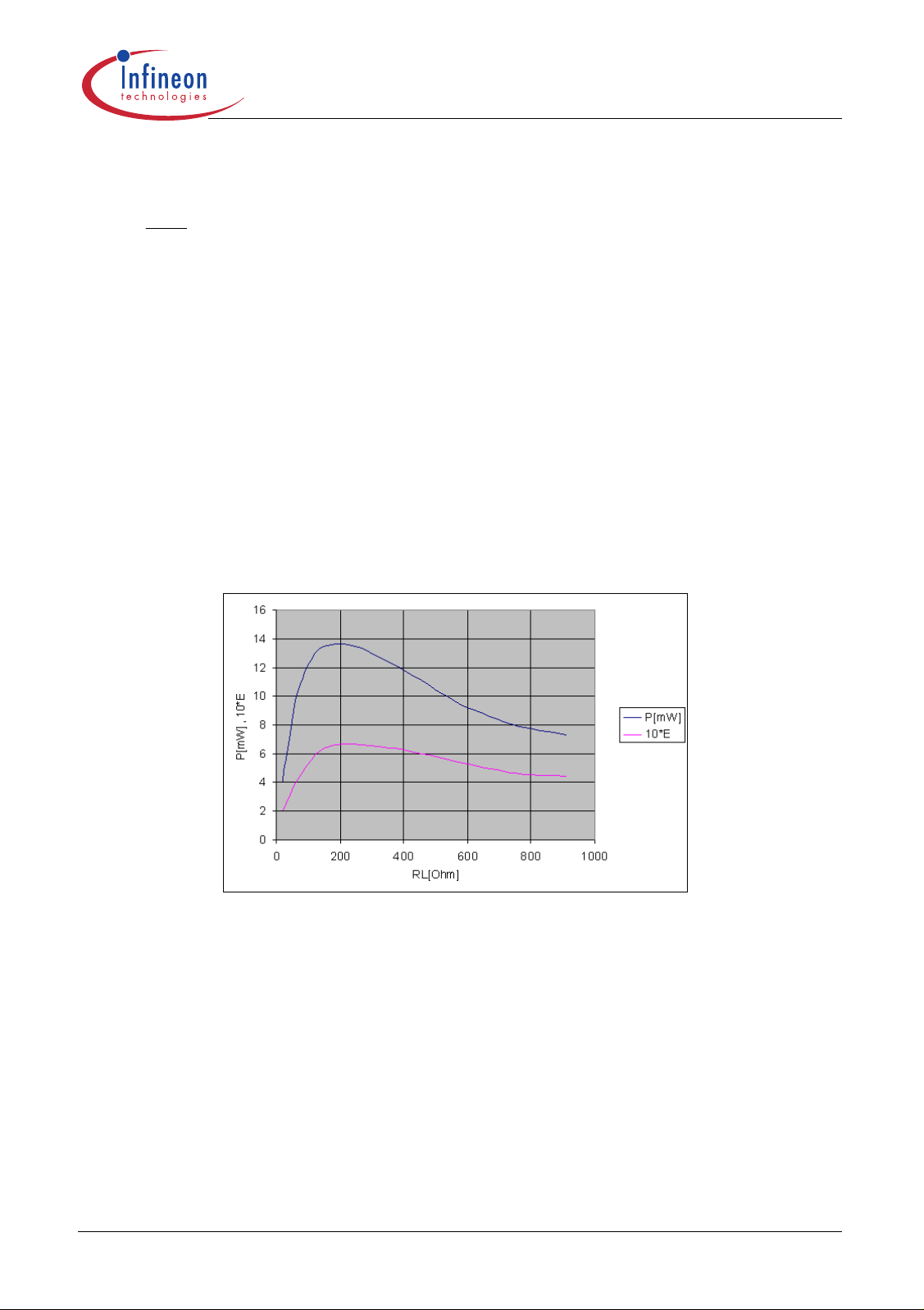
The diagram of Figure 3-7 has been measured directly at the PA-output at VS=3V. A power loss in
the matching circuit of about 2dB will decrease the output power. As shown in the diagram, 240
Ohm is the optimum impedance for operation at 3V. For an approximation of R
OPT
and P
OUT
at
other supply voltages those 2 formulas can be used:
[3 – 11]
OPT
S
VR ~
and
RP ~
OPTOUT
[3 – 12]
Power_E_vs_RL.wmf
Figure 3-7 Output power Po (mW) and collector efficiency E vs. load resistor RL.
The DC collector current Ic of the power amplifier and the RF output power Po vary with the load
resistor RL. This is typical for overcritical operation of class C amplifiers. The collector current will
show a characteristic dip at the resonance frequency for this type of “overcritical” operation. The
depth of this dip will increase with higher values of RL.
As Figure 3-8 shows, detuning beyond the bandwidth of the matching circuit results in a significant
increase of collector current of the power amplifier and in some loss of output power. This diagram
shows the data for the circuit of the test board at the frequency of 868 MHz. The effective load
resistor of this circuit is RL= 240Ohm, which is the optimum impedance for operation at 3V. This will
lead to a dip of the collector current f approx. 20%.
Data Sheet 45 2007-02-26

TDA5250 D2
Version 1.7
Figure 3-8 Power output and collector current vs. frequency
Application
pout_vs_frequ.wmf
C4, L2 and C3||C2 are the main matching components which are used to transform the 50 Ohm
load at the SMA-RF-connector to a higher impedance at the PA-output (240Ohm@3V). L1 can be
used for finetuning of the resonance frequency but should not be too low in order to keep its loss
low.
The transformed impedance of 240Ohm+j0 at the PA-output-pin can be verified with a network
analyzer using this measurement procedure:
1. Calibrate your network analyzer.
2. Connect a short, low-loss 50 Ohm cable to your network analyzer with an open end on one side.
Semirigid cable works best.
3. Use the „Port Extension“ feature of your network analyzer to shift the reference plane of your
network analyzer to the open end of the cable.
4. Connect the center-conductor of the cable to the solder pad of the pin „PA“ of the IC. The shield
has to be grounded. Very short connections must be used. Do not remove the IC or any part of
the matching-components!
5. Screw a 50Ohm-dummy-load on the RF-I/O-SMA-connector
6. The TDA5250 has to be in ASK-TX-Mode, Data-Input=LOW.
7. Be sure that your network analyzer is AC-coupled and turn on the power supply of the IC.
8. Measure the S-parameter
Data Sheet 46 2007-02-26

TDA5250 D2
Version 1.7
Application
Sparam_measured_200M.pcx
Figure 3-9 Sparam_measured_200M
Above you can see the measurement of the evalboard with a span of 200MHz. The evalboard has
been optimized for 3V. The load is about 240+j0 at 868.3MHz.
A tuning-free realization requires a careful design of the components within the matching network.
A simple linear CAE-tool will help to see the influence of tolerances of matching components.
Suppression of spurious harmonics may require some additional filtering within the antenna
matching circuit. Both can be seen in Figure 3-10 and Figure 3-11 The total spectrum of the
evalboard can be summarized as:
Carrier fc +9dBm
fc-18.1MHz -62dBm
fc+18.1MHz -66dBm
nd
2
harmonic -40dBm
rd
3
harmonic -44dBm
Data Sheet 47 2007-02-26

TDA5250 D2
Version 1.7
Figure 3-10 Transmit Spectrum 13.2GHz
Application
oberwellentx.tif
spektrum_10r_3v.tif
Figure 3-11 Transmit Spectrum 300MHz
Regarding CEPT ERC recommendation 70-03 and ETSI regulation EN 300220 both of the following
figures show full compliance in case of ASK and FSK modulation spectrum. Data signal is a
Manchester encoded PRBS9 (Pseudo Random Binary Sequence), RF output power is +9dBm at a
supply voltage of 3V. With these settings ASK allows a maximum data rate of 25kBaud, in FSK case
40kBaud are possible. See also Section 4.1.4
Data Sheet 48 2007-02-26

TDA5250 D2
Version 1.7
Application
ASK_25kBaud_Manch_PRBS9_10dBm_3V_Spectrum_CEPT_ERC7003.wmf
Figure 3-12 ASK Transmit Spectrum 25kBaud, Manch, PRBS9, 9dBm, 3V
FSK_40kBaud_Manch_PRBS9_10dBm_3V_Spectrum_CEPT_ERC7003.wmf
Figure 3-13 FSK Transmit Spectrum 40kBaud, Manch, PRBS9, 9dBm, 3V
Data Sheet 49 2007-02-26

TDA5250 D2
Version 1.7
Application
3.2 Crystal Oscillator
The equivalent schematic of the crystal with its parameters specified by the crystal manufacturer
can be taken from the subsequent figure.
Here also the load capacitance of the crystal CL, which the crystal wants to see in order to oscillate
at the desired frequency, can be seen.
C
1
R
1
C
1
0
C
L
Crystal.wmf
Figure 3-14 Crystal
L
-R
L
: motional inductance of the crystal
1
C
: motional capacitance of the crystal
1
C
: shunt capacitance of the crystal
0
Therefore the Resonant Frequency fs of the crystal is defined as:
S
*2
CL
π
11
1
=
f
[3 – 13]
The Series Load Resonant Frequency fS‘ of the crystal is defined as:
f
`
S
1
π
*2
CL
11
C
1*
1
+=
CC
+
L
0
[3 – 14]
regarding Figure 3-14
fs’ is the nominal frequency of the crystal with a specified load when tested by the crystal
manufacturer.
Pulling Sensitivity of the crystal is defined as the magnitude of the relative change in frequency
relating to the variation of the load capacitor.
Data Sheet 50 2007-02-26

TDA5250 D2
δ
Version 1.7
´
f
S
δ
D
δ
C
L
f
S
==
δ
C
L
C
−
1
()
2
2
CC
+
0
L
[3 – 15]
Application
Choosing CL as large as possible results in a small pulling sensitivity. On the other hand a small C
keeps the influence of the serial inductance and the tolerances associated to it small (see formula
[3-17]).
Start-up Time
t
Start
~
1
RR
−−
ext
[3 – 16]
L
where: -R: is the negative impedance of the oscillator
see Figure 3-15
R
: is the sum of all external resistances (e.g. R1 or any
ext
other resistance that may be present in the circuit,
see Figure 3-14
L
The proportionality of L1 and C1 of the crystal is defined by formula [3-13]. For a crystal with a small
C1 the start -up time will also be slower. Typically the lower the value of the crystal frequency, the
lower the C1.
A short conclusion regarding crystal and crystal oscillator dependencies is shown in the following
table:
Table 3-1 Crystal and crystal oscilator dependency
Result
Independent variable
C1 >
C0 >
frequency of quartz >
L
OSC
>
CL >
Relative Tolerance Maximum Deviation t
>> >> <
<< -
>>> > <<
>> > -
>< -
Start-up
The crystal oscillator in the TDA5250 is a NIC (negative impedance converter) oscillator type. The
input impedance of this oscillator is a negative impedance in series to an inductance. Therefore the
load capacitance of the crystal C
capacitance C
as shown in formula [3-17].
v
(specified by the crystal supplier) is transformed to the
L
Data Sheet 51 2007-02-26

TDA5250 D2
Version 1.7
-R
Figure 3-15 Crystal Oscillator
C
=
L
1
1
C
L
−
V
C
=↔
V
OSC
C
: crystal load capacitance for nominal frequency
L
1
C
ω: angular frequency
L
: inductivity of the crystal oscillator - typ: 2.7µH with pad of board
OSC
L
1
ωω
+
L
OSC
TDA 5250
22
L
OSC
f, C
C
L
V
2.45µH without pad
Application
QOSZ_NIC.wmf
[3 – 17]
With the aid of this formula it becomes obvious that the higher the serial capacitance CV is, the
higher is the influence of L
OSC
.
The tolerance of the internal oscillator inductivity is much higher, so the inductivity is the dominating
value for the tolerance.
FSK modulation and tuning are achieved by a variation of C
.
v
In case of small frequency deviations (up to +/- 1000 ppm), the desired load capacitances for FSK
modulation are frequency depending and can be calculated with the formula below.
−
CLC
+
C
L ±
------------------------------------------------------------------------------------------=
1
C
L
C
0
C
1
∆f
---------- 1
⋅⋅
0
Nf⋅
∆f
---------- 1
⋅±
Nf⋅
---------------------------------+
2C0CL+()⋅
---------------------------------+
C
1
C
1
: crystal load capacitance for nominal frequency
: shunt capacitance of the crystal
: motional capacitance of the crystal
[3 – 18]
2C0CL+()⋅
f: crystal oscillator frequency
N: division ratio of the PLL
Data Sheet 52 2007-02-26

TDA5250 D2
Version 1.7
Application
∆f: peak frequency deviation
With C
Alternatively, an external AC coupled (10nF in series to 1k
and CL- the necessary Cv+ for FSK HIGH and Cv- for FSK LOW can be calculated.
L+
Ω) signal can be applied at pin 19 (Xout).
The drive level should be approximately 100mVpp.
3.2.1 Synthesizer Frequency setting
Generating ASK and FSK modulation 3 setable frequencies are necessary.
3.2.1.1 Possible crystal oscillator frequencies
The resulting possible crystal oscillator frequencies are shown in the following Figure 3-16
RX: FSK ASK
TX: FSK- ASK FSK+
Deviation Deviation
f
1
f
0
Nominal
Frequency
f
2
free_reg.wmf
Figure 3-16 possible crystal oscillator frequencies
In ASK receive mode the crystal oscillator is set to frequency f
offset to receive the ASK signal at f
To set the 3 different frequencies 3 different C
*N (N: division ratio of the PLL).
0
are necessary. Via internal switches 3 external
v
capacitors can be combined to generate the necessary C
to realize the necessary frequency
2
in case of ASK- or FSK-modulation.
v
Internal banks of switchable capacitors allow the finetuning of these frequencies.
3.2.2 Transmit/Receive ASK/FSK Frequency Assignment
Depending on whether the device operates in transmit or receive mode or whether it operates in
ASK or FSK the following cases can be distinguished:
3.2.2.1 FSK-mode
In transmit mode the two frequencies representing logical HIGH and LOW data states have to be
adjusted depending on the intended frequency deviation and separately according to the following
formulas:
Data Sheet 53 2007-02-26

TDA5250 D2
Version 1.7
f
COSC HI
= (fRF + f
) / 48 f
DEV
COSC LOW
= (fRF - f
DEV
) / 48
[3 – 19]
Application
e.g.
f
COSC HI
f
COSC LOW
= (868,3E6 + 50E3) / 48 = 18.08438MHz
= (868,3E6 - 50E3) / 48 = 18.08229MHz
with a frequency deviation of 50kHz.
Figure 3-17 shows the configuration of the switches and the capacitors to achieve the 2 desired
frequencies. Gray parts of the schematics indicate inactive parts. For FSK modulation the ASKswitch is always open.
For FSK LOW the FSK-switch is closed and C
and C
v2
are bypassed. The effective Cv- is given
tune2
by:
−
For finetuning C
CCC +=
11 tunevV
can be varied over a range of 8 pF in steps of 125fF. The switches of this C-
tune1
[3 – 20]
bank are controlled by the bits D0 to D5 in the FSK register (subaddress 01H, see Table 3-6).
For FSK HIGH the FSK-switch is open. So the effective C
C
C
v+
The C-bank C
+()C
v1Ctune1
---------------------------------------------------------------------------------------=
Cv1C
+C
tune1
can be varied over a range of 16 pF in steps of 250fF for finetuning of the FSK
tune2
+()⋅
v2Ctune2
++
v2Ctune2
is given by:
v+
[3 – 21]
HIGH frequency. The switches of this C-bank are controlled by the bits D8 to D13 in the FSK
register (subaddress 01H, see Table 3-6).
XOUT 19
f, C
L
XIN 21
C
V1
XSWF 20
XSWA 22
C
C
V2
V3
XGND 23
-RL
C
V1
C
tune1
C
V2
C
tune2
f, C
C
XOUT 19
L
XIN 21
XSWF 20
XSWA 22
V3
XGND 23
-RL
C
tune1
C
tune2
ASK-
switch
FSK LOW
FSK-
switch
ASK-
switch
FSK HIGH
FSK-
switch
Data Sheet 54 2007-02-26

TDA5250 D2
Version 1.7
Application
QOSC_FSK.wmf
Figure 3-17 FSK modulation
In receive mode the crystal oscillator frequency is set to yield a direct-to-zero conversion of the
receive data. Thus the frequency may be calculated as
f
= fRF / 48,
COSC
e.g.
f
= 868,3E6 / 48 = 18.0833MHz
COSC
[3 – 22]
which is identical to the ASK transmit case.
-RL
C
tune1
C
tune2
C
V1
C
V2CV3
f, C
XOUT 19
L
XIN 21
XSWF 20
XSWA 22
XGND 23
ASK-
switch
FSK-
switch
QOSC_ASK.wmf
Figure 3-18 FSK receive
In this case the ASK-switch is closed. The necessary C
C
The C-bank C
+()Cv2C+
C
vm
tune2
v1Ctune1
--------------------------------------------------------------------------------------------------------=
C
+C
v1Ctune1
v2
can be varied over a range of 16 pF in steps of 250fF for finetuning of the FSK
C
+()⋅
tune2
v3
C+
C
++
tune2
v3
is given by:
vm
[3 – 23]
receive frequency. In this case the switches of the C-bank are controlled by the bits D0 to D5 of the
XTAL_TUNING register (subaddress 02H, see Table 3-5).
3.2.2.2 ASK-mode:
In transmit mode the crystal oscillator frequency is the same as in the FSK receive case, see
Figure 3-18.
In receive mode a receive frequency offset is necessary as the limiters feedback is AC-coupled.
This offset is achieved by setting the oscillator frequency to the FSK HIGH transmit frequency, see
Figure 3-17.
Data Sheet 55 2007-02-26

TDA5250 D2
Version 1.7
Application
3.2.3 Parasitics
For the correct calculation of the external capacitors the parasitic capacitances of the pins and the
switches (C
, C21, C22) have to be taken into account.
20
XOUT 19
f, C
L
XIN 21
C
V1
XSWF 20
XSWA 22
C
C
V2
V3
XGND 23
C
22
-RL
C
21
C
tune1
C
C
tune2
20
Figure 3-19 parasitics of the switching network
Table 3-2 Typical values of parasitic capacitances
Name
C
20
C
21
C
22
With the given parasitics the actual C
C
C
v-
Cv1C
+()C
C
C
vm
v+
C
v1Ctune1
----------------------------------------------------------------------------------------------------------------------------------------- C21+=
C
v1Ctune1
------------------------------------------------------------------------------------------------------- C21+=
C
+()C
tune1
+C
v1Ctune1
+C
++=
v1Ctune1C21
v2C20
v2C20
v2C20
v2C20
FSK-: 2,8 pF / FSK+&ASK: 2.3pF
can be calculated:
v
+()⋅
++
C+
tune2
C+
tune2
C++v3C22C+
+()⋅
C++v3C22C+
++
Value
4,5 pF
1,3 pF
tune2
tune2
QOSC_parasitics.wmf
[3 – 24]
[3 – 26]
Data Sheet 56 2007-02-26

TDA5250 D2
Version 1.7
Note: Please keep in mind also to include the Pad parasitics of the circuit board.
Application
[3 – 25][3 – 25]
3.2.4 Calculation of the external capacitors
1. Determination of necessary crystal frequency using formula [4-19].
e.g. f
2. Determine corresponding C
e.g. C
3. Necessary CV using formula [4-17].
e.g.
1. When the necessary Cv for the 3 frequencies (Cv- for FSK LOW, Cv+ for FSK HIGH and Cvm for
FSK-receive) are known the external capacitors and the internal tuning caps can be calculated
using the following formulas:
FSK-
L FSK
= f
COSC LOW
- = C
C
V
−
applying formula [4-18].
Load
L ±
=
1
C
FSKL
,−−
1
()
+
π
2
Lf
*2
OSCFSK
-FSK:
+FSK:
FSK_RX:
C
C
C
+C
v1
v2Ctune2
tune1
+
v-C21
C
v1
---------------------------------------------------------------------- C20–=
C
v1
C
C
v3
C
+
tune2
-------------------------------------------------------------------------C
C
v1Ctune1
–=
C
+()C
tune1
C
+()C
tune1
C
+()C
v1
tune1
+()C
–()⋅
v+C21
–()–
v+C21
C21–()⋅
vm
C21–()–
vm
–C
–C
20
To compensate frequency errors due to crystal and component tolerance C
–=
v2
v1
22
, Cv2 and Cv3 have to
[3 – 27]
[3 – 28]
[3 – 29]
be varied. To enable this correction, half of the necessary capacitance variation has to be realized
with the internal C-banks.
If no finetuning is intended it is recommended to leave XIN (Pin 21) open. So the parasitic
capacitance of Pin 21 has no effect.
Note: Please keep in mind also to include the Pad parasitics of the circuit board.
In the suitable range for the serial capacitor, either capacitors with a tolerance of 0.1pF or 1% are
available.
A spreadsheet, which can be used to predict the total frequency error by simply entering the crystal
specification, may be obtained from Infineon.
3.2.5 FSK-switch modes
The FSK-switch can be used either in a bipolar or in a FET mode. The mode of this switch is
controlled by bit D0 of the XTAL_CONFIG register (subaddress 0EH).
Data Sheet 57 2007-02-26

TDA5250 D2
Version 1.7
In the bipolar mode the FSK-switch can be controlled by a ramp function. This ramp function is set
by the bits D1 and D2 of the XTAL_CONFIG register (subadress 0EH). With these modes of the
FSK-switch the bandwidth of the FSK spectrum can be influenced.
When working in the FET mode the power consumption can be reduced by about 200
The default mode is bipolar switch with no ramp function (D0 = 1, D1 = D2 = 0), which is suitable
for all bitrates.
Table 3-3 Sub Address 0EH: XTAL_CONFIG
D0
0
1
1
1
1
D1 D2 Switch mode Ramp time Max. Bitrate
n.a. n.a. FET < 0.2 µs > 32 kBit/s NRZ
00bipolar (default) < 0.2 µs > 32 kBit/s NRZ
10 bipolar 4 µs 32 kBit/s NRZ
01 bipolar 8 µs 16 kBit/s NRZ
11 bipolar 12 µs 12 kBit/s NRZ
Application
µA.
3.2.6 Finetuning and FSK modulation relevant registers
Case FSK-RX or ASK-TX (C
tune2
):
Table 3-4 Sub Address 02H: XTAL_TUNING
Bit
D5
D4 Nominal_Frequ_4 4pF 1
D3 Nominal_Frequ_3 2pF 0
D2 Nominal_Frequ_2 1pF ASK-TX
D1 Nominal_Frequ_1 500fF 1
D0 Nominal_Frequ_0 250fF
Case FSK-TX or ASK-RX (C
Table 3-5 Sub Address 01H: FSK
Bit
D13 FSK+5 8pF Setting for
D12 FSK+4 4pF 0
D11 FSK+3 2pF 1
D10 FSK+2 1pF 0
D9 FSK+1 500fF 1
D8 FSK+0 250fF
Function Value Description Default
Nominal_Frequ_5 8pF Setting for
nominal
frequency
FSK-RX
(C
and C
tune1
Function Value Description Default
tune2
):
positive
frequency
shift: +FSK
or ASK-RX
(C
tune2
tune2
)
)
0
0
0
0
0
Data Sheet 58 2007-02-26

TDA5250 D2
Version 1.7
D5 FSK-5 4pF Setting for
D4 FSK-4 2pF 0
D3 FSK-3 1pF 1
D2 FSK-2 500fF 1
D1 FSK-1 250fF 0
D0 FSK-0 125fF
Default values
In case of using the evaluation board, the crystal with its typical parameters (fp=18.08958MHz,
C
=8fF, C0=2,08pF, CL=12pF) and external capacitors with Cv1=4.7pF, Cv2=1.8pF, Cv3=12pF
1
each are used the following default states are set in the device
Table 3-6 Default oscillator settings
Operating state
ASK-TX / FSK-RX
+FSK-TX / ASK-RX
-FSK-TX
Frequency
868.3 MHz
+50 kHz
-50 kHz
negative
frequency
shift: -FSK
(C
tune1
.
)
Application
0
0
3.2.7 Chip and System Tolerances
Quartz: fp=18.08958MHz; C1=8fF; C0=2,08pF; CL=12pF (typical values)
Cv1=4.7pF, Cv2=1.8pF, Cv3=12pF
Table 3-7 Internal Tuning
Part
Frequency set accuracy
Temperature (-40...+85C)
Supply Voltage(2.1...5.5V)
Total
Table 3-8 Default Setup (without internal tuning & without Pin21 usage)
Part
Internal capacitors (+/- 10%)
Inductivity of the crystal oscillator
Temperature (-40...+85C)
Supply Voltage (2.1...5.5V)
Total
Frequency tolerance
@ 868MHz
+/- 3kHz +/- 3.5ppm
+/- 5kHz +/- 6ppm
+/- 1.5kHz +/- 1.5ppm
+/- 9.5kHz +/- 11ppm
Frequency tolerance
@ 868MHz
+/- 8kHz +/- 9ppm
+/- 18kHz +/- 21ppm
+/- 5kHz +/- 6ppm
+/- 1kHz +/- 1.5ppm
+/- 32kHz +/- 37.5ppm
Rel. tolerance
Rel. tolerance
Tolerance values in Table 3-8 are valid, if pin 21 is not connected. Establishing the connection to
pin 21 the tolerances increase by +/- 20ppm (internal capacitors), if internal tuning is not used.
Data Sheet 59 2007-02-26

TDA5250 D2
Version 1.7
Concerning the frequency tolerances of the whole system also crystal tolerances (tuning
tolerances, temperature stability, tolerance of CL) have to be considered.
In addition to the chip tolerances also the crystal and external component tolerances have to be
considered in the tuning and non-tuning case.
In case of internal tuning: The crystal on the evaluation board has a temperature stability of +/20ppm (or +/- 17kHz), which must be added to the total tolerances.
In case of default setup (without internal tuning and without usage of pin 21) the temperature
stability and tuning tolerance of the crystal as well as the tolerance of the external capacitors (+/-
0.1pF) have to be added. The crystal on the evaluation board has a temperature stability of +/20ppm (or +/- 17kHz) and a tuning tolerance of +/- 10ppm (or +/- 8.5 kHz).The external capacitors
add a tolerance of +/- 4ppm (or +/- 3.5kHz).
The frequency stabilities of both the receiver and the transmitter and the modulation bandwidth set
the limit for the bandwidth of the IQ filter. To achieve a high receiver sensitivity and efficient
suppression of adjacent interference signals, the narrowest possible IQ bandwidth should be
realized (see Section 3.3).
Application
3.3 IQ-Filter
The IQ-Filter should be set to values corresponding to the RF-bandwidth of the received RF signal
via the D1 to D3 bits of the LPF register (subaddress 03H).
Table 3-9 3dB cutoff frequencies I/Q Filter
D3
0
0 0 1 350 700
0
0
1
1
1
1
D2 D1 nominal f
(programmable)
0 0 not used
1 0 250 500
1 1 200 400
0 0 150 (default) 300
0 1 100 200
1 0 50 100
1 1 not used
-3dB
in kHz
resulting effective
channel
bandwidth in kHz
Data Sheet 60 2007-02-26

TDA5250 D2
Version 1.7
10
0
-10
-20
-30
-40
-50
-60
-70
-80
10 10 0 10 0 0 10 0 0 0
Figure 3-20 I/Q Filter Characteristics
effective channel bandwidth
Application
50 kHz
10 0 k Hz
15 0 k H z
200kHz
250kHz
350kHz
f [kHz]
iq_filter_curve.wmf
-f
f
3dB
IQ Filter
f
3dB
IQ Filter
f
iq_char.wmf
Figure 3-21 IQ Filter and frequency characteristics of the receive system
3.4 Data Filter
The Data-Filter should be set to values corresponding to the bandwidth of the transmitted Data
signal via the D4 to D7 bits of the LPF register (subaddress 03H).
Data Sheet 61 2007-02-26

TDA5250 D2
Version 1.7
Table 3-10 3dB cutoff frequencies Data Filter
D7
0
0
0
0
0
0
0
0
1
1
1
1
1
1
1
1
D6 D5 D4 nominal f
0 0 0 5
0 0 1 7 (default)
0 1 0 9
0 1 1 11
1 0 0 14
1 0 1 18
1 1 0 23
1 1 1 28
0 0 0 32
0 0 1 39
0 1 0 49
0 1 1 55
1 0 0 64
1 0 1 73
1 1 0 86
1 1 1 102
-3dB
Application
in kHz
3.5 Limiter and RSSI
The I/Q Limiters are DC coupled multistage amplifiers with offset-compensating feedback circuit
and an overall gain of approximately 80dB each in the frequency range of 100Hz up to 350kHz.
Receive Signal Strength Indicator (RSSI) generators are included in both limiters which produce DC
voltages that are directly proportional to the input signal level in the respective channels. The
resulting I- and Q-channel RSSI-signals are summed to the nominal RSSI signal.
C
c
I- Filter
C
c
38
37
CI1x
CI1
f
g
36 35 34
CQ1
C
c
CI2
CQ1x
Limiter
C
c
CQ2
33 32 31
CI2x
I
C
RSSI
CQ2x
Quadr.
Corr.
RSSI29
37k
Σ
Q- Filter
Q
f
g
Limiter
Quadr.
Corr.
limiter input.wmf
Figure 3-22 Limiter and Pinning
Data Sheet 62 2007-02-26

TDA5250 D2
Version 1.7
Application
The DC offset compensation needs 2.2ms after Power On or Tx/Rx switch. This time is hard wired
and independent from external capacitors CC on pins 31 to 38. The maximum value for this
capacitors is 47nF.
RSSI accuracy settling time = 2.2ms + 5*RC=2.2ms+5*37k*2.2nF=2.6ms
R - internal resistor; C - external capacitor at Pin 29
Table 3-11 Limiter Bandwidth
Cc
[nF]
220
100
47
22
f3dB
lower limit
[Hz]
f3dB
upper
limit
Comment
100 IQ Filter setup time not guaranteed
220 - ll - setup time not guaranteed
470 - ll - Eval Board
1000 - ll -
10 2200 - ll -
v [dB]
80
0
f
3dB
f
3dB
IQ Filter
Figure 3-23 Limiter frequency characteristics
f
3dB
Limiterlower limit
f
limiter_char.wmf
Data Sheet 63 2007-02-26

TDA5250 D2
Version 1.7
1300
1200
1100
1000
900
800
700
600
RSSI /mV
500
400
300
200
100
0
-120 -110 - 100 -90 -80 -7 0 -60 -50 -40 -3 0 -20
Figure 3-24 Typ. RSSI Level (Eval Board) @3V
RF / dB m
Application
ADC
high gain
low gain
RSSI.wmf
3.6 Data Slicer - Slicing Level
The data slicer is an analog-to-digital converter. It is necessary to generate a threshold value for the
negative comparator input (data slicer). The TDA5250 offers an RC integrator and a peak detector
which can be selected via logic. Independent of the choice, the peak detector outputs are always
active.
3.6.1 RC Integrator
Table 3-12 Sub Address 00H: CONFIG
Bit
D15
Necessary external component (Pin14): C
This integrator generates the mean value of the data filter output. For a stable threshold value, the
cut-off frequency has to be lower than the lowest signal frequency. The cutoff frequency results from
the internal resistance R=100k
Cut-off frequency:
Function Description Default SET
SLICER 0= LP, 1= Peak Detector 0 0
SLC
Ω and the external capacitor C
f <
=
offcut
−
1
1002
π
Ck
⋅Ω⋅
SLC
on Pin14.
SLC
{}
fMin
Signal
[3 – 30]
Component calculation: (rule of thumb)
T
– longest period of no signal change
L
⋅
T
3
100
L
Ω
k
≥
C
SLC
[3 – 31]
Data Sheet 64 2007-02-26

TDA5250 D2
Version 1.7
Figure 3-25 Slicer Level using RC Integrator
Application
SLC_RC.wmf
3.6.2 Peak Detectors
Table 3-13 Sub Address 00H: CONFIG
Bit
D15
The TDA5250 has two peak detectors built in, one for positive peaks in the data stream and the
other for the negative ones.
Necessary external components: - Pin12: C
Function Description Default SET
SLICER 0= LP, 1= Peak Detector 0 1
N
- Pin13: C
P
Data Sheet 65 2007-02-26

TDA5250 D2
⋅Ω=
τ
Version 1.7
Figure 3-26 Slicer Level using Peak Detector
Application
SLC_PkD.wmf
For applications requiring fast attack and slow release from the threshold value it is reasonable to
use the peak detectors. The threshold value is generated by an internal voltage divider. The release
time is defined by the internal resistance values and the external capacitors.
[3 – 32]
[3 – 33]
Signal
Signal
τ
τ
negPkD
100
Ck
Ck ⋅Ω=100
τ
pposPkD
nnegPkD
posPkD
Pos. Peak Detector (pin13)
Threshold SLC(pin14)
Neg. Peak Detector (pin12)
t
PkD_timing.wmf
Figure 3-27 Peak Detector timing
Data Sheet 66 2007-02-26

TDA5250 D2
Version 1.7
Application
Component calculation: (rule of thumb)
T2
⋅
C
p
C
n
L1
≥
100k
Ω
– longest period of no signal change (LOW signal)
T
L1
T2
⋅
L2
≥
100k
Ω
– longest period of no signal change (HIGH signal)
T
L2
[3 – 34]
[3 – 35]
3.6.3 Peak Detector - Analog output signal
The TDA5250 data output can be digital (pin 28) or in analog form by using the peak detector output
and changing some settings.
To get an analog data output the slicer must be set to lowpass mode (Reg. 0, D15 = LP = 0) and
the peak detector capacitor at pin 12 or 13 has to be changed to a resistor of about 47kOhm.
PkD_analog.wmf
Figure 3-28 Peak Detector as analog Buffer (v=1)
3.6.4 Peak Detector – Power Down Mode
For a safe and fast threshold value generation the peak detector is turned on by the sequencer
circuit (see Section 2.4.18) only after the entire receiving path is active.
In the off state the output of the positive peak detector is tied down to GND and the output of the
negative peak detector is pulled up to VCC.
Data Sheet 67 2007-02-26

TDA5250 D2
Version 1.7
Figure 3-29 Peak detector - power down mode
Application
PKD_PWDN.wmff
Signal
Data Signal
Vcc
0
Power ON Power Down
Neg. Peak Detector (pin12)
Threshold (pin14)
Pos. Peak Detector (pin13)
2,2ms
Power ON
Peak Detector Power ON
t
PkD_PWDN3.wmf
Figure 3-30 Power down mode
3.7 Data Valid Detection
In order to detect valid data two criteria must be fulfilled.
One criteria is the data rate, which can be set in register 06h and 07h. The other one is the received
RF power level, which can be set in register 08h in form of the RSSI threshold voltage. Thus for
using the data valid detection FSK modulation is recommended.
Data Sheet 68 2007-02-26

TDA5250 D2
Version 1.7
Application
Timing for data detection looks like the following. Two settings are possible: „Continuous“ and
„Single Shot“, which can be set by D5 and D6 in register 00H.
Data
Sequenzer enables
data detection
Counter Reset
Gate time
Compare with single
TH and latch result
Compare with double
TH and latch result
(Frequency) Window
Count Complete
resetreset
count count
comp. comp.
comp.
ready*
start of conversion possible start of next conversion
Frequ_Detect_Timing_continuous.wmf
t
t
t
t
t
t
t
Figure 3-31 Frequency Detection timing in continuous mode
Note 1: Chip internal signal „Sequencer enables data detection“ has a LOW to HIGH transition
about 2.6ms after RX is activated (see Figure 2-15).
Note 2: The positive edge of the „Window Count Complete“ signal latches the result of comparison
of the analog to digital converted RSSI voltage with TH3 (register 08H). A logic combination of this
output and the result of the comparison with single/double THx defines the internal signal
„data_valid“.
Figure 3-31 shows that the logic is ready for the next conversion after 3 periods of the data signal.
Timing in Single Shot mode can be seen in the subsequent figure:
Data
Sequenzer enables
data detection
Counter Reset
Gate time
Compare with single
TH and latch result
Compare with double
TH and latch result
(Frequency) Window
Count Complete
start of conversion
reset
count
no possible start of n ext conversion
comp.
comp.
ready*
because of Single Shot Mode
t
t
t
t
t
t
t
Frequ_Detect_Timing_singleShot_wmf
Figure 3-32 Frequency Detection timing in Single Shot mode
Data Sheet 69 2007-02-26

TDA5250 D2
Version 1.7
Application
3.7.1 Frequency Window for Data Rate Detection
The high time of data is used to measure the frequency of the data signal. For Manchester coding
either the data frequency or half of the data frequency have to be detected corresponding to one
high time or twice the high time of data signal.
A time period of 3*2*T is necessary to decide about valid or invalid data.
T2*T
DATA
possible
GATE 1
possible
GATE 2
0010
T2
T1
0
2*T2
2*T1
01
t
t
t
window_count_timing.wmf
Figure 3-33 Window Counter timing
Example to calculate the thresholds for a given data rate:
- Data signal manchester coded
- Data Rate: 2kbit//s
- f
= 18,0896 MHz
clk
Then the period equals to
1
T2 ==⋅
2kbit/s
0,5ms
[3 – 36]
respectively the high time is 0,25ms.
We set the thresholds to +-10% and get: T1= 0,225ms and T2= 0,275ms
The thresholds TH1 and TH2 are calculated with following formulas
f
clk
T1TH1
⋅=
[3 – 37]
4
f
clk
T2TH2
⋅=
[3 – 38]
4
Data Sheet 70 2007-02-26

TDA5250 D2
Version 1.7
Application
This yields the following results:
TH1~ 1017= 001111111001
TH2~ 1243= 010011011011
b
b
which have to be programmed into the D0 to D11 bits of the COUNT_TH1 and COUNT_TH2
registers (subaddresses 06H and 07H), respectively.
Default values (window counter inactive):
TH1= 000000000000
TH2= 000000000001
b
b
Note: The timing window of +-10% of a given high time T in general does not correspond to a
frequency window +-10% of the calculated data frequency.
3.7.2 RSSI threshold voltage - RF input power
The RF input power level is corresponding to a certain RSSI voltage, which can be seen in Section
3.5. The threshold TH3 of this RSSI voltage can be calculated with the following formula:
TH3
1.2V
voltagethresholdRSSIdesired
)12(6−⋅=
[3 – 39]
As an example a desired RSSI threshold voltage of 500mV results in TH3~26=011010b, which has
to be written into D0 to D5 of the RSSI_TH3 register (sub address 08H).
Default value (RSSI detection inactive):
TH3=111111
b
3.8 Calculation of ON_TIME and OFF_TIME
ON= (216-1)-(fRC*tON)
OFF=( 2
f
RC
Example: t
16
-1)-(fRC*t
OFF
)
= Frequency of internal RC Oszillator
= 0,005s, t
ON
= 0,055s, fRC= 32300Hz
OFF
ON= 65535-(32300*0,005) ~ 65373= 1111111101011101
OFF= 65535-(32300*0,055) ~ 63758= 1111100100001110
[3 – 40]
[3 – 41]
b
b
The values have to be written into the D0 to D15 bits of the ON_TIME and OFF_TIME registers
(subaddresses 04H and 05H).
Data Sheet 71 2007-02-26

TDA5250 D2
Version 1.7
Application
Default values:
ON= 65215 = 1111111011000000
OFF= 62335 = 1111001110000000
b
b
tON ~10ms @ fRC= 32kHz
t
~100ms @ fRC= 32kHz
OFF
3.9 Example for Self Polling Mode
The settings for Self Polling Mode depend very much on the timing of the transmitted Signal. To
create an example we consider following data structure transmitted in FSK.
4 Frames
Data Data Data Data
50ms 50m s
400ms
t [ms]
Frame-
details
Sync
Preamble
Syncronisation Preamble
Data
t [ms]
t [ms]
data_timing011.wmf
Figure 3-34 Example for transmitted Data-structure
According to existing synchronization techniques there are some synchronization bursts in front of
the data added (code violation!). A minimum of 4 Frames is transmitted. Data are preferably
Manchester encoded to get fastest respond out of the Data Rate Detection.
Target Application:
- received Signal has code violation as described before
- total mean current consumption below 1mA
- data reception within max. 400ms after first transmitted frame
One possible Solution:
tON = 15ms, t
= 135ms
OFF
Data Sheet 72 2007-02-26

TDA5250 D2
Version 1.7
Application
This gives 15ms ON time of a total period of 150ms which results in max. 0.9mA mean current
consumption in Self Polling Mode. The resulting worst case timing is shown in the following figure:
Case A:
Case B:
Case C:
Data Data Data Data
50ms 135ms15ms µP enables Receiver
Data Data Data Data
50ms
Data Data Data Data
50ms
... Receiver enabled
135ms15ms
135ms15ms
until Data completed
Interrupt
due PwdDD
µP enables Receiver
until Data completed
Interrupt
due PwdDD
µP enables Receiver
until Data completed
Interrupt
due PwdDD
t [ms]
t [ms]
t [ms]
data_timing021.wmf
Figure 3-35 3 possible timings
Description:
Assumption: the ON time comes right after the first frame (Case A). If OFF time is 135ms the
receiver turns on during Sync-pulses and the PwdDD
- pulse wakes up the µP.
If the ON time is in the center of the 50ms gap of transmission (Case B), the Data Detect Logic will
wake up the µP 135ms later.
If ON time is over just before Sync-pulses (Case C), next ON time is during Data transmission and
Data Detect Logic will trigger a PwdDD
- pulse to wake up the µP.
Note: In this example it is recommended to use the Peak Detector for slicer threshold generation,
because of its fast attack and slow release characteristic. To overcome the data zero gap of 50ms
larger external capacitors than noted in Section 4.4 at pin12 and 13 are recommended. Further
information on calculating these components can be taken from Section 3.6.2.
3.10 Sensitivity Measurements
3.10.1 Test Setup
The test setup used for the measurements is shown in the following figure. In case of ASK
modulation the Rohde & Schwarz SMIQ generator, which is a vector signal generator, is connected
to the I/Q modulation source AMIQ. This "baseband signal generator" is in turn controlled by the PC
Data Sheet 73 2007-02-26
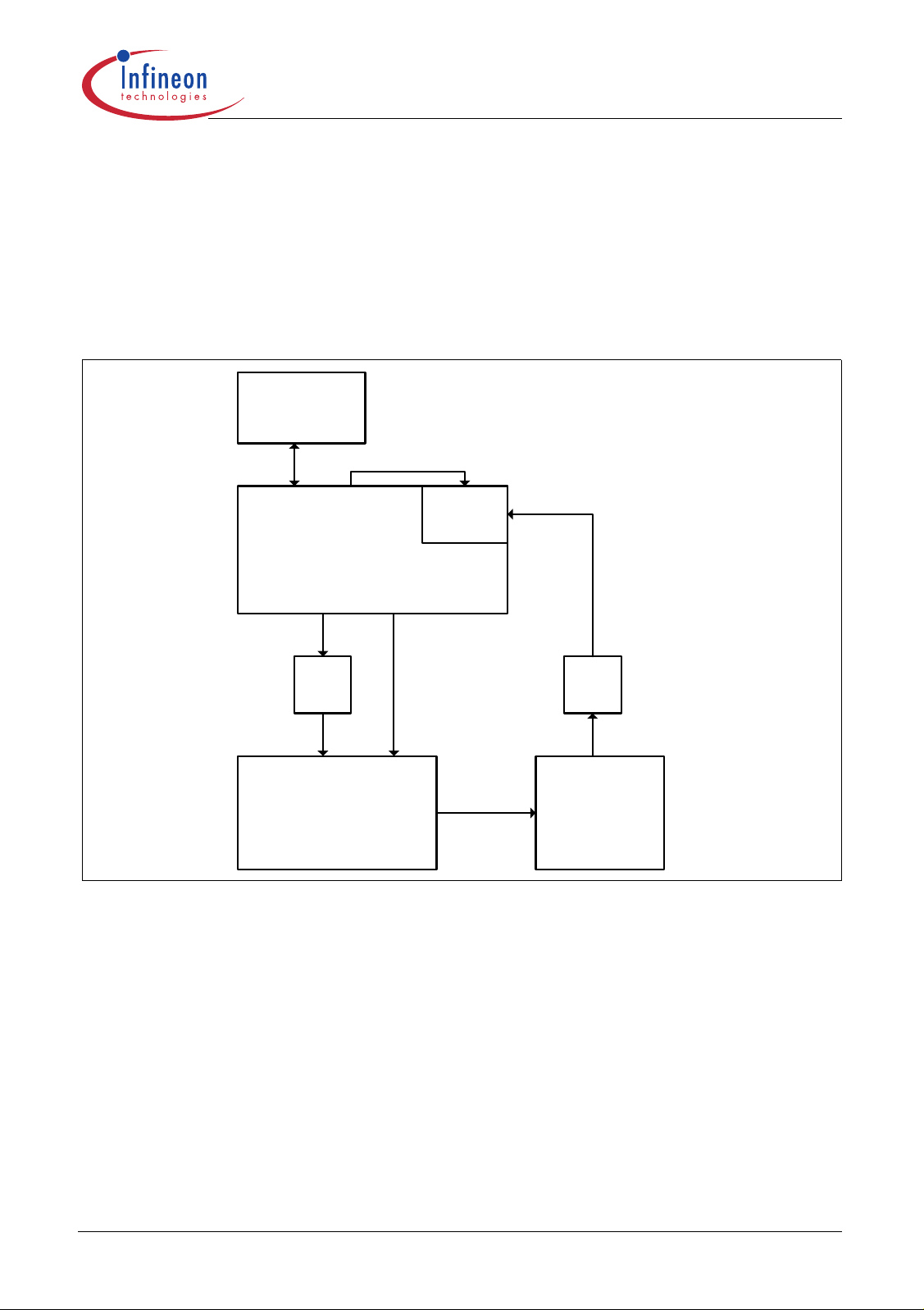
TDA5250 D2
Version 1.7
Application
based software WinQSIM via a GPIB interface. The AMIQ generator has a pseudo random binary
sequence (PRBS) generator and a bit error test set built in. The resulting I/Q signals are applied to
the SMIQ to generate a ASK (OOK) spectrum at the desired RF frequency.
Data is demodulated by the TDA5250 and then sent back to the AMIQ to be compared with the
originally sent data. The bit error rate is calculated by the bit error rate equipment inside the AMIQ.
Baseband coding in the form of Manchester is applied to the I signal as can be seen in the
subsequent figure.
Personal Computer
Software
WinIQSIM
GPIB /
RS 232
Marker Output
Rohde & Schwarz
I/Q Modulation Source
AMIQ
I
Q
AMIQ BERT
(Bit Error Rate
Test Set)
Clock
Data
Manchester
Encoder
Rohde & Schwarz
Vector Signal Generator
SMIQ 03
ASK / FSK RF Signal
Manchester
Decoder
DATAout
RFin
DUT
Transceiver Testboard
TDA5250
TestSetup.wmf
Figure 3-36 BER Test Setup
In the following figures the RF power level shown is the average power level.
These investigations have been made on an Infineon evaluation board using a data rate of 4 kBit/
s with manchester encoding and a data filter bandwidth of 7 kHz. This is the standard configuration
of our evaluation boards. All these measurements have been performed with several evaluation
boards, so that production scattering and component tolerances are already included in these
results.
Regarding the data filter bandwidth it has to be mentioned that a data rate of 4 kBit/s using
manchester encoding results in a data frequency of 2 kHz to 4 kHz depending on the occurring
data pattern. The test pattern given by the AMIQ is a pseudo random binary sequency (PRBS9)
with a 9 bit shift register. This pattern varies the resulting data frequency up to 4 kHz.
Data Sheet 74 2007-02-26

TDA5250 D2
Version 1.7
The best sensitivity performance can be achieved using a data filter bandwidth of 1.25 times the
maximum occuring data frequency.
The IQ filter setting is depending on the modulation type. ASK needs an IQ filter of 50kHz, 50kHz
deviation at FSK recommend a 100kHz IQ filter and 100kHz deviation were measured with a
150kHz IQ filter
A very practicable configuration is to set the chip-internal adjustable IQ filter to the sum of FSK peak
deviation and maximum datafrequency. Concerning these aspects the bandwidth should be chosen
small enough. With respect to both, the crystal tolerances and the tolerances of the crystal oscillator
circuit of receiver and transmitter as well, a too small IQ filter bandwidth will reduce the sensitivity
again. So a compromise has to be made. For further details on chip tolerances see also Section
3.2.7
Application
3.10.2 Sensitivity depending on the ambient Temperature
Demonstrating a wide band of application possibilities the temperature behavior must not be
forgotten. In automotive systems the required temperature range is from -40 °C to +85 °C. The
receivers very good performance is documented in the following graph. The selected supply
voltage is 5V, the influence of the supply voltage can be seen in the following Section 3.10.3
The IQ filter setting can be taken from the legend of Figure 3-37.
BER_Temp_5V.wmf
Figure 3-37 Temperature Behaviour
Figure 3-37 shows that ASK as well as FSK sensitivity is in the range of -110 to -111dBm at 20°C
ambient temperature for a BER of 2E-3.
Notice that the sensitivity variation in this temperature range of -40 °C to +85 °C is only about 1.5
to 2 dB.
Data Sheet 75 2007-02-26

TDA5250 D2
Version 1.7
Application
3.10.3 BER performance depending on Supply Voltage
Due to the wide supply voltage range of this transeiver chip also the sensitivity behaviour over this
parameter is documented is the subsequent graph.
BER_VCC_20°C..wmf
Figure 3-38 BER supply voltage
Please notice the tiny sensitivity changes of 1.5 to 2.5dB, when variing the supply voltage.
3.10.4 Datarates and Sensitivity
The TDA 5250 can handle datarates up to 64kbit/s, as can be taken from the following figure. (see
Section 4.1.4)
Data Sheet 76 2007-02-26

TDA5250 D2
Version 1.7
Figure 3-39 Datarates and Sensitivity
Application
BER_Datarate.wmf
3.10.5 Sensitivity at Frequency Offset
Applying the test setup in Figure 3-36 even a wide offset in the received frequency spectrum results
only in a slight decrease of receiving sensitivity. At an offset of 100kHz one of the two 50kHz FSK
peaks is at the 3dB border of the IQ filter (150kHz), which is the reason for the decline of the
sensitivity (see point A in Figure 3-40).
A frequency offset of 50kHz (FSK deviation: 50kHz) increases the data jitter of the demodulated
signal and therefore results in little loss of sensitivity (see point B in Figure 3-40).
In this case one of the peaks of the FSK-spectrum lies in the DC-blocking notch of the baseband
limiters.
BER_FrequOffset_FSK_3V..wmf
Figure 3-40 BER Frequency Offset
Data Sheet 77 2007-02-26

TDA5250 D2
Version 1.7
Application
3.11 Default Setup
Default setup is hard wired on chip and effective after a reset or return of power supply.
Table 3-14 Default Setup
Parameter
IQ-Filter Bandwidth 150kHz
Data Filter Bandwidth 7kHz
Limiter lower fg 470Hz 47nF
Slicing Level Generation RC 10nF
Nom. Frequency Capacity intern (ASK TX, FSK RX) 4.5pF 868.3MHz
FSK+ Frequency Capacity intern (FSK+, ASK RX) 2.5pF +50kHz
FSK- Frequency Capacity intern (FSK-) 1.5pF -50kHz
LNA Gain HIGH
Power Amplifier HIGH +10dBm
Value IFX-Board Comment
RSSI accuracy settling time 2.6ms 2.2nF
ADC measurement RSSI
ON-Time 10ms
OFF-Time 100ms
Clock out RX PowerON 1MHz
Clock out TX PowerON 1MHz
Clock out RX PowerDOWN -
Clock out TX PowerDOWN -
XTAL modulation switch bipolar
XTAL modulation shaping off
RX / TX - Jumper
ASK/FSK - Jumper
PwdDD PWDN Jumper
removed
Operating Mode Slave
Data Sheet 78 2007-02-26

TDA5250 D2
Version 1.7
4 Reference
4.1 Electrical Data
4.1.1 Absolute Maximum Ratings
WARNING
The maximum ratings may not be exceeded under any circumstances, not even
momentarily and individually, as permanent damage to the IC will result.
Table 4-1 Absolute Maximum Ratings
#
1 Supply Voltage V
2 Junction Temperature T
3 Storage Temperature T
4 Thermal Resistance R
5 ESD integrity, all pins V
6
ESD integrity, except pin
7
Parameter Symbol Limit Values Unit Remarks
s
j
s
thJA
ESD-CDM
V
ESD-HBM
8, 9, 11, 15, 18, 23, 30
ESD integrity, of pin
8, 9, 11, 15, 18, 23, 30
V
ESD-HBM
Reference
min max
-0.3 5.8 V
-40 +125 °C
-40 +150 °C
114 K/W
-1.5 +1.5 kV CDM according
EIA/JESD22-C101
-2.0 +2.0 kV HBM according
EIA/JESD22-A114-B
(1.5k
Ω, 100pF)
-500 +500 V HBM according
EIA/JESD22-A114-B
(1.5k
Ω, 100pF)
4.1.2 Operating Range
Within the operational range the IC operates as explained in the circuit description.
Table 4-2 Operating Range
#
1 Supply voltage
2 Ambient temperature T
3 Receive frequency f
4 Transmit frequency f
Data Sheet 79 2007-02-26
Parameter Symbol Limit Values Unit Test Conditions L Item
min max
V
S
A
RX
TX
2.1 5.5 V
-40 85 °C
868 870 MHz
868 870 MHz

TDA5250 D2
Version 1.7
Reference
4.1.3 AC/DC Characteristics
AC/DC characteristics involve the spread of values guaranteed within the specified voltage and
ambient temperature range. Typical characteristics are the median of the production.
Table 4-3 AC/DC Characteristics with TA = 25 °C, V
#
Parameter Symbol Limit Values Unit Test Conditions L Item
min typ max
RECEIVER Characteristics
1
Supply current RX FSK I
2 Supply current RX FSK I
3 Supply current RX ASK I
4 Supply current RX ASK I
5 Sensitivity FSK
-3
10
BER
6 Sensitivity ASK
-3
10
BER
RX_FSK
RX_FSK
RX_ASK
RX_ASK
RF
sens
RF
sens
9 mA 3V, FSK, Default
9.5 mA 5V, FSK, Default
8.6 mA 3V, ASK, Default
9.1 mA 5V, ASK, Default
-109 dBm FSK@50kHz, 4kBit/s
-109 dBm ASK, 4kBit/s Manch.
= 2.1 ... 5.5 V
VCC
Manch. Data, Default
7kHz datafilter, 100kHz
IQ filter
data, Default setup
7kHz datafilter,
50kHz IQ filter
■
■
7 Power down current I
8 System setup time (1st
PWDN_RX
t
SYSSU
4812 ms
5 nA 5.5V, all power down
power on or reset)
9 Clock Out setup time t
CLKSU
0.5 ms stable CLKDIV output
signal
10 Receiver setup time t
RXSU
1.54 2.2 2.86 ms DATA out (valid or
invalid)
11 Data detection setup
t
DDSU
1.82 2.6 3.38 ms Begin of Data detection
time
12 RSSI stable time t
RSSI
1.82 2.6 3.38 ms RFin -100dBm
see chapter 4.5
13 Data Valid time t
Data_Valid
3.35 ms 4kBit/s Manch.
detected (valid)
14 Input P
15 Input P
16 Selectivity V
17 LO leakage P
, high gain P
1dB
, low gain P
1dB
1dB
1dB_low
BL_1MHz
LO
-48dBm dBm 3V, Default, high gain ■
-32dBm dBm 3V, Default, low gain ■
50 dB fRF+/-1MHz, Default,
RF
sens
+3dB
■
-98 dBm 1157.73MHz ■
Data Sheet 80 2007-02-26

TDA5250 D2
Version 1.7
Table 4-3 AC/DC Characteristics with TA = 25 °C, V
#
TRANSMITTER Characteristics
1
Supply current TX, FSK I
2
Supply current TX, FSK I
3
Supply current TX, FSK I
4 Output power P
5 Output power P
6 Output power P
7 Supply current TX, FSK I
8
Supply current TX, FSK I
9
Supply current TX, FSK I
Parameter Symbol Limit Values Unit Test Conditions L Item
min typ max
TX
TX
TX
out
out
out
TX
TX
TX
9.4 mA 2.1V, high power 1
11.9 mA 3V, high power 1
14.6 mA 5V, high power 1
6 dBm 2.1V, high power ■
9 dBm 3V, high power ■
13 dBm 5V, high power ■
4.1 mA 2.1V, low power 1
4.9 mA 3V, low power 1
6.8 mA 5V, low power 1
= 2.1 ... 5.5 V
VCC
Reference
10 Output power P
11 Output power P
12 Output power P
13 Power down current I
14 Clock Out setup time t
15 Transmitter setup time t
16 Spurious fRF+/-f
17 Spurious fRF+/-f
clock
XTAL
18 Spurious 2nd harmonic P
19 Spurious 3rd harmonic P
1: without pin diode current (RX/TX-switch)
130uA@2.1V; 310uA@3V; 720uA@5V
out_low
out_low
out_low
PWDN_TX
CLKSU
TXSU
P
clock
P
1st
2nd
3rd
-30 dBm 2.1V, low power ■
-22 dBm 3V, low power ■
-3 dBm 5V, low power ■
5 nA 5.5V, all power down
0.5 ms stable CLKDIV output
signal
0.77 1.1 1.43 ms PWDN-->PON or
RX-->TX
dBm 3V, 50Ohm Board,
Default (1MHz)
-66 dBm 3V, 50Ohm Board ■
-40 dBm 3V, 50Ohm Board ■
-50 dBm 3V, 50Ohm Board ■
■
■
Data Sheet 81 2007-02-26

TDA5250 D2
Version 1.7
Table 4-4 AC/DC Characteristics with TA = 25 °C, V
#
GENERAL Characteristics
1 Power down current
2 Power down current
3 Power down current with
4 Power down current with
5 32kHz oscillator freq. f
Parameter Symbol Limit Values Unit Test Conditions L Item
min typ max
I
PWDN_32k
9 uA 3V, 32kHz clock on
timer mode (standby)
I
PWDN_32k
11 uA 5V, 32kHz clock on
timer mode (standby)
I
PWDN_Xtl
750 uA 3V, CONFIG9=1
XTAL ON
I
PWDN_Xtl
860 uA 5V, CONFIG9=1
XTAL ON
32kHz
24 32 40 kHz
= 2.1 ... 5.5 V
VCC
Reference
6 XTAL startup time t
7 Load capacitance C
8 Serial resistance of the
R
crystal
9 Input inductance XOUT L
10 Input inductance XOUT L
11 FSK demodulator gain G
12 RSSI@-120dBm U
13 RSSI@-100dBm U
-120dBm
-100dBm
14 RSSI@-70dBm U
15 RSSI@-50dBm U
16 RSSI Gradient G
17 IQ-Filter bandwidth f
18 Data Filter bandwidth f
3dB_IQ
3dB_LP
XTAL
C0max
Rmax
OSC
OSC
FSK
-70dBm
-50dBm
RSSI
0.5 ms IFX Board with Crystal
■
Q1 as specified in
Section 4.4
5 pF ■
100 W ■
2.7 uH with pad on evaluation
■
board
2.45 uH without pad on evalution
■
board
2.4 mV/
kHz
0.35 V default setup ■
0.55 V default setup ■
1 V default setup ■
1.2 V default setup ■
14 mV/
default setup ■
dB
115 150 185 kHz Default setup ■
5.3 7 8.7 kHz Default setup ■
19 Vcc-Vtune RX, Pin3 V
20 Vcc-Vtune TX, Pin3 V
cc-tune,RX
cc-tune,TX
0.5 1 1.6 V f
0.5 1.1 1.6 V f
=18.08956MHz
Ref
=18.08956MHz
Ref
Data Sheet 82 2007-02-26

TDA5250 D2
Version 1.7
4.1.4 Digital Characteristics
I2C Bus Timing
BusMode = LOW
t
BUF
Bus D at a
t
R
t
LOW
t
HIGH
t
HD.STA
t
SU.ENAS DA
t
HD.DAT
t
HIGH
BusCLK
EN
pulsed or
mandatory low
t
SU.ENAS DA
Reference
t
t
F
t
SU.DAT
t
SU.STA
HD.STA t
SP
t
SU.S TO
t
SU.ENA SDA
Figure 4-1 I
2
C Bus Timing
3-wire Bus Timing
BUS_MODE = HI GH
SDA
t
t
LOW
R
SCL
t
SU.STA
t
HD.DAT
BUS_ENA
t
WHEN
Figure 4-2 3-wire Bus Timing
t
HIGH
t
t
F
t
SU.DAT
SP
t
SU.ST O
Data Sheet 83 2007-02-26

TDA5250 D2
Version 1.7
Table 4-5 Digital Characteristics with TA = 25 °C, V
#
1 Data rate TX ASK f
2
3
4
5 Data rate RX FSK f
6 Digital Inputs
High-level Input Voltage
7 RXTX Pin 5
TX operation, int. controlled
8 CLKDIV Pin 26
t
Parameter Symbol Limit Values Unit Test Conditions L Item
min typ max
10 25 kBaud PRBS9,
10 64 kBaud PRBS9,
10 40 kBaud PRBS9,
10 64 kBaud PRBS9, Manch. ■
10 64 kBaud PRBS9,
0.4
Data rate TX ASK f
Data rate TX FSK f
Data rate RX ASK f
Low-level Input Voltage
TX.ASK
TX.ASK
TX.FSK
RX.ASK
RX.FSK
V
IH
V
IL
V
OL
V
dd
-0.35
0
1.15
rise
t
fall
(0.1*V
(0.9*V
to 0.9*Vdd)
dd
to 0.1*Vdd)
dd
Output High Voltage
Output Low Voltage
t
r
t
f
V
OH
V
OL
35
30
V
dd
-0.4
0.4
= 2.1 ... 5.5 V
Vdd
V
dd
0.35VV
V
V
ns
ns
V
V
Manch.@+10dBm
Manch.@-5dBm
Manch.@+10dBm
@50kHz dev.
Manch.@100kHz
dev.
@Vdd=3V
Isink=800uA
Isink=3mA
@Vdd=3V
load 10pF
load 10pF
Isource=350uA
Isink=400uA
Reference
■ 1
■ 1
■ 1
■
■
■
■
Bus Interface Characteristics
9 Pulse width of spikes which
t
SP
0 50 ns V
=5V ■
dd
must be suppressed by the
input filter
10 LOW level output voltage at
BusData
11 SLC clock frequency f
12 Bus free time between
STOP and START condition
13 Hold time (repeated)
START condition.
Table 4-5 Digital Characteristics with TA = 25 °C, V
V
OL
SLC
t
BUF
t
HO.STA
0.4 V 3mA sink current
V
=5V
dd
0 400 kHz V
=5V ■
dd
1.3 µs only I2C mode
=5V
V
dd
0.6 µs After this period, the
first clock pulse is
2
C
= 2.1 ... 5.5 V
Vdd
generated, only I
■
■
■
Data Sheet 84 2007-02-26

TDA5250 D2
Version 1.7
Reference
# Parameter Symbol Limit Values Unit Test Conditions L Item
min typ max
14 LOW period of BusCLK
t
LOW
1.3 µs V
=5V ■
dd
clock
15 HIGH period of BusCLK
t
HIGH
0.6 µs V
=5V ■
dd
clock
16 Setup time for a repeated
t
SU.STA
0.6 µs only I
2
C mode ■
START condition
17 Data hold time t
18 Data setup time t
19 Rise, fall time of both
BusData and BusCLK
HD.DAT
SU.DAT
tR, t
F
0 ns V
100 ns V
20+
0.1C
b
300 ns V
=5V ■
dd
=5V ■
dd
=5V ■ 2
dd
signals
20
21 Capacitive load for each bus
Setup time for STOP
condition
t
SU.STO
C
b
0.6 µs only I2C mode
V
=5V
dd
400 pF V
=5V ■
dd
■
line
22 Setup time for BusCLK to ENt
23 H-pulsewidth (EN) t
SU.SCL
EN
WHEN
0.6 µs only 3-wire mode
V
=5V
dd
0.6 µs V
=5V ■
dd
■
1: limited by transmission channel bandwidth and depending on transmit power level; ETSI regulation EN 300 220
fullfilled,
2: Cb= capacitance of one bus line
see Section 3.1
Data Sheet 85 2007-02-26

TDA5250 D2
Version 1.7
Reference
4.2 Test Circuit
The device performance parameters marked with ■ in Section 4.1.3 were measured on an Infineon
evaluation board (IFX board).
TDA5250_v42.schematic.pdf
Figure 4-3 Schematic of the Evaluation Board
Data Sheet 86 2007-02-26

TDA5250 D2
Version 1.7
4.3 Test Board Layout
Gerberfiles for this Testboard are available on request.
Reference
TDA5250_v42_layout.pdf
Figure 4-4 Layout of the Evaluation Board
Note 1: The LNA and PA matching network was designed for minimum required space and
maximum performance and thus via holes were deliberately placed into solder pads.
In case of reproduction please bear in mind that this may not be suitable for all automatic soldering
processes.
Note 2: Please keep in mind not to layout the CLKDIV line directly in the neighborhood of the crystal
and the associated components.
Data Sheet 87 2007-02-26

TDA5250 D2
Version 1.7
4.4 Bill of Materials
Table 4-6 Bill of Materials
Reference
R1
R2
R3
R4
R5
R6
R7
R8
R9
R10
R11
R12
R13
R14
R15
R16
R17
R18
R19
R20
R21
R22
R23
R24
C1
C2
C3
C4
C5
C6
C7
C8
C9
C10
C11
C12
C13
Reference
Value Specification Tolerance
4k7 0603 +/-5%
10Ω 0603 +/-5%
--- 0603 +/-5%
1M 0603 +/-5%
4k7 0603 +/-5%
4k7 0603 +/-5%
4k7 0603 +/-5%
6k8 0603 +/-5%
180 0603 +/-5%
180 0603 +/-5%
270 0603 +/-5%
15k 0603 +/-5%
10k 0603 +/-5%
180 0603 +/-5%
180 0603 +/-5%
1M 0603 +/-5%
1M 0603 +/-5%
1M 0603 +/-5%
560 0603 +/-5%
1k 0603 +/-5%
10 0603 +/-5%
00603 +/-5%
10 0603 +/-5%
180 0603 +/-5%
22pF 0603 +/-1%
1pF 0603 +/-0,1pF
5,6pF 0603 +/-0,1pF
2,2pF 0603 +/-0,1pF
1nF 0603 +/-5%
1nF 0603 +/-5%
15pF 0603 +/-1%
--- 0603 +/-0,1pF
47pF 0603 +/-1%
22pF 0603 +/-1%
--- 0603 +/-5%
10nF 0603 +/-10%
10nF 0603 +/-10%
Data Sheet 88 2007-02-26

TDA5250 D2
Version 1.7
Table 4-6 Bill of Materials
Reference
C14
C15
C16
C17
C18
C19
C20
C21
C22
C23
C24
C25
C26
C27
C28
C29
C30
L1
L2
L3
IC1
IC2 ILQ74
IC3 SFH6186
Q1 18.08958MHz Telcona: C0=2,1pF C1=8fF, CL=12pF
S1
T1 BC847B SOT-23 (Infineon)
D1, D2 BAR63-02W SCD-80 (Infineon)
X1, X2 SMA-socket
X5 SubD 25p.
Reference
Value Specification Tolerance
10nF 0603 +/-10%
4.7pF 0603 +/-0,1pF
1.8pF 0603 +/-0,1pF
12pF 0603 +/-1%
10nF 0603 +/-10%
2,2nF 0603 +/-10%
47nF 0603 +/-10%
47nF 0603 +/-10%
47nF 0603 +/-10%
47nF 0603 +/-10%
100nF 0603 +/-10%
100nF 0603 +/-10%
--- 0603 +/-10%
100nF 0603 +/-10%
100nF 0603 +/-10%
100nF 0603 +/-10%
--- 0603 +/-10%
68nH SIMID 0603-C (EPCOS) +/-2%
12nH SIMID 0603-C (EPCOS) +/-2%
8.2nH SIMID 0603-C (EPCOS) +/-0.2nH
TDA5250 D2 PTSSOP38
1-pol.
Data Sheet 89 2007-02-26

TDA5250 D2
Version 1.7
List of Tables
Table 2-1 Pin Definition and Function . . . . . . . . . . . . . . . . . . . . . . . . . . . . . . . . page 12
Table 2-2 Sub Address 00H: CONFIG . . . . . . . . . . . . . . . . . . . . . . . . . . . . . . . page 19
Table 2-3 Sub Address 00H: CONFIG . . . . . . . . . . . . . . . . . . . . . . . . . . . . . . . page 19
Table 2-4 Sub Address 00H: CONFIG . . . . . . . . . . . . . . . . . . . . . . . . . . . . . . . page 22
Table 2-5 PwdDD Pin Operating States . . . . . . . . . . . . . . . . . . . . . . . . . . . . . . page 23
Table 2-6 Bus Interface Format. . . . . . . . . . . . . . . . . . . . . . . . . . . . . . . . . . . . . page 24
Table 2-7 Chip address Organization . . . . . . . . . . . . . . . . . . . . . . . . . . . . . . . . page 25
Table 2-8 I2C Bus Write Mode 8 Bit . . . . . . . . . . . . . . . . . . . . . . . . . . . . . . . . . page 26
Table 2-9 I2C Bus Write Mode 16 Bit . . . . . . . . . . . . . . . . . . . . . . . . . . . . . . . . page 26
Table 2-10 I2C Bus Read Mode. . . . . . . . . . . . . . . . . . . . . . . . . . . . . . . . . . . . . page 26
Table 2-11 3-wire Bus Write Mode . . . . . . . . . . . . . . . . . . . . . . . . . . . . . . . . . . . page 27
Table 2-12 3-wire Bus Read Mode . . . . . . . . . . . . . . . . . . . . . . . . . . . . . . . . . . . page 27
Table 2-13 Sub Addresses of Data Registers Write. . . . . . . . . . . . . . . . . . . . . . page 28
Table 2-14 Sub Addresses of Data Registers Read. . . . . . . . . . . . . . . . . . . . . . page 28
Table 2-15 Sub Address 00H: CONFIG . . . . . . . . . . . . . . . . . . . . . . . . . . . . . . . page 28
Table 2-16 Sub Addresses of Data Registers Write. . . . . . . . . . . . . . . . . . . . . . page 29
Table 2-17 Sub Addresses of Data Registers Read. . . . . . . . . . . . . . . . . . . . . . page 29
Table 2-18 Sub Address 00H: CONFIG . . . . . . . . . . . . . . . . . . . . . . . . . . . . . . . page 29
Table 2-19 Sub Address 01H: FSK . . . . . . . . . . . . . . . . . . . . . . . . . . . . . . . . . . . page 30
Table 2-20 Sub Address 02H: XTAL_TUNING . . . . . . . . . . . . . . . . . . . . . . . . . . page 30
Table 2-21 Sub Address 03H: LPF. . . . . . . . . . . . . . . . . . . . . . . . . . . . . . . . . . . page 30
Table 2-22 Sub Addresses 04H / 05H: ON/OFF_TIME . . . . . . . . . . . . . . . . . . . page 30
Table 2-23 Sub Address 06H: COUNT_TH1 . . . . . . . . . . . . . . . . . . . . . . . . . . . page 30
Table 2-24 Sub Address 07H: COUNT_TH2 . . . . . . . . . . . . . . . . . . . . . . . . . . . page 30
Table 2-25 Sub Address 08H: RSSI_TH3 . . . . . . . . . . . . . . . . . . . . . . . . . . . . . page 31
Table 2-26 Sub Address 0DH: CLK_DIV . . . . . . . . . . . . . . . . . . . . . . . . . . . . . . page 31
Table 2-27 Sub Address 0EH: XTAL_CONFIG . . . . . . . . . . . . . . . . . . . . . . . . . page 31
Table 2-28 Sub Address 0FH: BLOCK_PD . . . . . . . . . . . . . . . . . . . . . . . . . . . . page 31
Table 2-29 Sub Address 80H: STATUS. . . . . . . . . . . . . . . . . . . . . . . . . . . . . . . page 31
Table 2-30 Sub Address 81H: ADC . . . . . . . . . . . . . . . . . . . . . . . . . . . . . . . . . . page 31
Table 2-31 MODE settings: CONFIG register . . . . . . . . . . . . . . . . . . . . . . . . . . page 32
Table 2-32 CLK_DIV Output Selection. . . . . . . . . . . . . . . . . . . . . . . . . . . . . . . . page 37
Table 2-33 CLK_DIV Setting . . . . . . . . . . . . . . . . . . . . . . . . . . . . . . . . . . . . . . . page 37
Table 2-34 Source for 6Bit-ADC Selection (Register 08H). . . . . . . . . . . . . . . . . page 37
Table 3-1 Crystal and crystal oscilator dependency . . . . . . . . . . . . . . . . . . . . . page 51
Table 3-2 Typical values of parasitic capacitances . . . . . . . . . . . . . . . . . . . . . . page 56
Table 3-3 Sub Address 0EH: XTAL_CONFIG. . . . . . . . . . . . . . . . . . . . . . . . . . page 58
Table 3-4 Sub Address 02H: XTAL_TUNING . . . . . . . . . . . . . . . . . . . . . . . . . . page 58
Table 3-5 Sub Address 01H: FSK . . . . . . . . . . . . . . . . . . . . . . . . . . . . . . . . . . . page 58
Table 3-6 Default oscillator settings . . . . . . . . . . . . . . . . . . . . . . . . . . . . . . . . . page 59
Table 3-7 Internal Tuning . . . . . . . . . . . . . . . . . . . . . . . . . . . . . . . . . . . . . . . . . page 59
Table 3-8 Default Setup (without internal tuning & without Pin21 usage) . . . . . page 59
Table 3-9 3dB cutoff frequencies I/Q Filter . . . . . . . . . . . . . . . . . . . . . . . . . . . . page 60
Data Sheet 90 2007-02-26

TDA5250 D2
Version 1.7
List of Tables
Table 3-10 3dB cutoff frequencies Data Filter . . . . . . . . . . . . . . . . . . . . . . . . . . page 62
Table 3-11 Limiter Bandwidth . . . . . . . . . . . . . . . . . . . . . . . . . . . . . . . . . . . . . . . page 63
Table 3-12 Sub Address 00H: CONFIG . . . . . . . . . . . . . . . . . . . . . . . . . . . . . . . page 64
Table 3-13 Sub Address 00H: CONFIG . . . . . . . . . . . . . . . . . . . . . . . . . . . . . . . page 65
Table 3-14 Default Setup . . . . . . . . . . . . . . . . . . . . . . . . . . . . . . . . . . . . . . . . . . page 78
Table 4-1 Absolute Maximum Ratings. . . . . . . . . . . . . . . . . . . . . . . . . . . . . . . . page 79
Table 4-2 Operating Range. . . . . . . . . . . . . . . . . . . . . . . . . . . . . . . . . . . . . . . . page 79
Table 4-3 AC/DC Characteristics with TA = 25 °C, VVCC = 2.1 ... 5.5 V . . . . . page 80
Table 4-4 AC/DC Characteristics with TA = 25 °C, VVCC = 2.1 ... 5.5 V . . . . . page 82
Table 4-5 Digital Characteristics with TA = 25 °C, VVdd = 2.1 ... 5.5 V . . . . . . page 84
Table 4-6 Bill of Materials . . . . . . . . . . . . . . . . . . . . . . . . . . . . . . . . . . . . . . . . . page 88
Data Sheet 91 2007-02-26

TDA5250 D2
Version 1.7
List of Figures
Figure 1-1 PG-TSSOP-38 package outlines. . . . . . . . . . . . . . . . . . . . . . . . . . . . page 10
Figure 2-1 Pin Configuration. . . . . . . . . . . . . . . . . . . . . . . . . . . . . . . . . . . . . . . . page 11
Figure 2-2 Main Block Diagram . . . . . . . . . . . . . . . . . . . . . . . . . . . . . . . . . . . . . page 18
Figure 2-3 One I/Q Filter stage. . . . . . . . . . . . . . . . . . . . . . . . . . . . . . . . . . . . . . page 20
Figure 2-4 Quadricorrelator Demodulation Characteristic . . . . . . . . . . . . . . . . . page 21
Figure 2-5 Data Filter architecture . . . . . . . . . . . . . . . . . . . . . . . . . . . . . . . . . . . page 22
Figure 2-6 Timing and Data Control Unit . . . . . . . . . . . . . . . . . . . . . . . . . . . . . . page 23
Figure 2-7 Bus Interface . . . . . . . . . . . . . . . . . . . . . . . . . . . . . . . . . . . . . . . . . . . page 24
Figure 2-8 Sub Addresses Overview . . . . . . . . . . . . . . . . . . . . . . . . . . . . . . . . . page 27
Figure 2-9 Wakeup Logic States . . . . . . . . . . . . . . . . . . . . . . . . . . . . . . . . . . . . page 32
Figure 2-10 Timing for Self Polling Mode (ADC & Data Detect in one shot mode) page 32
Figure 2-11 Timing for Timer Mode . . . . . . . . . . . . . . . . . . . . . . . . . . . . . . . . . . . page 33
Figure 2-12 Frequency and RSSI Window . . . . . . . . . . . . . . . . . . . . . . . . . . . . . . page 33
Figure 2-13 Data Valid Circuit. . . . . . . . . . . . . . . . . . . . . . . . . . . . . . . . . . . . . . . . page 34
Figure 2-14 Data Input/Output Circuit. . . . . . . . . . . . . . . . . . . . . . . . . . . . . . . . . . page 34
Figure 2-15 1
Figure 2-16 1st start or reset in PD mode. . . . . . . . . . . . . . . . . . . . . . . . . . . . . . . page 35
Figure 2-17 Sequencer‘s capability . . . . . . . . . . . . . . . . . . . . . . . . . . . . . . . . . . . page 36
Figure 2-18 Clock Divider . . . . . . . . . . . . . . . . . . . . . . . . . . . . . . . . . . . . . . . . . . . page 36
Figure 3-1 RX/TX Switch . . . . . . . . . . . . . . . . . . . . . . . . . . . . . . . . . . . . . . . . . . page 39
Figure 3-2 RX-Mode . . . . . . . . . . . . . . . . . . . . . . . . . . . . . . . . . . . . . . . . . . . . . . page 40
Figure 3-3 S11 measured . . . . . . . . . . . . . . . . . . . . . . . . . . . . . . . . . . . . . . . . . . page 41
Figure 3-4 TX_Mode. . . . . . . . . . . . . . . . . . . . . . . . . . . . . . . . . . . . . . . . . . . . . . page 43
Figure 3-5 TX_Mode_simplified . . . . . . . . . . . . . . . . . . . . . . . . . . . . . . . . . . . . . page 43
Figure 3-6 Equivalent power amplifier tank circuit . . . . . . . . . . . . . . . . . . . . . . . page 44
Figure 3-7 Output power Po (mW) and collector efficiency E vs. load resistor RL. page 45
Figure 3-8 Power output and collector current vs. frequency . . . . . . . . . . . . . . . page 46
Figure 3-9 Sparam_measured_200M. . . . . . . . . . . . . . . . . . . . . . . . . . . . . . . . . page 47
Figure 3-10 Transmit Spectrum 13.2GHz. . . . . . . . . . . . . . . . . . . . . . . . . . . . . . . page 48
Figure 3-11 Transmit Spectrum 300MHz . . . . . . . . . . . . . . . . . . . . . . . . . . . . . . . page 48
Figure 3-12 ASK Transmit Spectrum 25kBaud, Manch, PRBS9, 9dBm, 3V . . . . page 49
Figure 3-13 FSK Transmit Spectrum 40kBaud, Manch, PRBS9, 9dBm, 3V . . . . page 49
Figure 3-14 Crystal . . . . . . . . . . . . . . . . . . . . . . . . . . . . . . . . . . . . . . . . . . . . . . . . page 50
Figure 3-15 Crystal Oscillator . . . . . . . . . . . . . . . . . . . . . . . . . . . . . . . . . . . . . . . . page 52
Figure 3-16 possible crystal oscillator frequencies . . . . . . . . . . . . . . . . . . . . . . . . page 53
Figure 3-17 FSK modulation. . . . . . . . . . . . . . . . . . . . . . . . . . . . . . . . . . . . . . . . . page 55
Figure 3-18 FSK receive. . . . . . . . . . . . . . . . . . . . . . . . . . . . . . . . . . . . . . . . . . . . page 55
Figure 3-19 parasitics of the switching network . . . . . . . . . . . . . . . . . . . . . . . . . . page 56
Figure 3-20 I/Q Filter Characteristics . . . . . . . . . . . . . . . . . . . . . . . . . . . . . . . . . . page 61
Figure 3-21 IQ Filter and frequency characteristics of the receive system. . . . . . page 61
Figure 3-22 Limiter and Pinning . . . . . . . . . . . . . . . . . . . . . . . . . . . . . . . . . . . . . . page 62
Figure 3-23 Limiter frequency characteristics. . . . . . . . . . . . . . . . . . . . . . . . . . . . page 63
Figure 3-24 Typ. RSSI Level (Eval Board) @3V . . . . . . . . . . . . . . . . . . . . . . . . . page 64
st
start or reset in active mode . . . . . . . . . . . . . . . . . . . . . . . . . . . . . page 35
Data Sheet 92 2007-02-26

TDA5250 D2
Version 1.7
List of Figures
Figure 3-25 Slicer Level using RC Integrator . . . . . . . . . . . . . . . . . . . . . . . . . . . . page 65
Figure 3-26 Slicer Level using Peak Detector . . . . . . . . . . . . . . . . . . . . . . . . . . . page 66
Figure 3-27 Peak Detector timing . . . . . . . . . . . . . . . . . . . . . . . . . . . . . . . . . . . . . page 66
Figure 3-28 Peak Detector as analog Buffer (v=1). . . . . . . . . . . . . . . . . . . . . . . . page 67
Figure 3-29 Peak detector - power down mode . . . . . . . . . . . . . . . . . . . . . . . . . . page 68
Figure 3-30 Power down mode. . . . . . . . . . . . . . . . . . . . . . . . . . . . . . . . . . . . . . . page 68
Figure 3-31 Frequency Detection timing in continuous mode . . . . . . . . . . . . . . . page 69
Figure 3-32 Frequency Detection timing in Single Shot mode . . . . . . . . . . . . . . . page 69
Figure 3-33 Window Counter timing . . . . . . . . . . . . . . . . . . . . . . . . . . . . . . . . . . . page 70
Figure 3-34 Example for transmitted Data-structure. . . . . . . . . . . . . . . . . . . . . . . page 72
Figure 3-35 3 possible timings . . . . . . . . . . . . . . . . . . . . . . . . . . . . . . . . . . . . . . . page 73
Figure 3-36 BER Test Setup. . . . . . . . . . . . . . . . . . . . . . . . . . . . . . . . . . . . . . . . . page 74
Figure 3-37 Temperature Behaviour. . . . . . . . . . . . . . . . . . . . . . . . . . . . . . . . . . . page 75
Figure 3-38 BER supply voltage . . . . . . . . . . . . . . . . . . . . . . . . . . . . . . . . . . . . . . page 76
Figure 3-39 Datarates and Sensitivity. . . . . . . . . . . . . . . . . . . . . . . . . . . . . . . . . . page 77
Figure 3-40 BER Frequency Offset . . . . . . . . . . . . . . . . . . . . . . . . . . . . . . . . . . . page 77
Figure 4-1 I2C Bus Timing . . . . . . . . . . . . . . . . . . . . . . . . . . . . . . . . . . . . . . . . . page 83
Figure 4-2 3-wire Bus Timing . . . . . . . . . . . . . . . . . . . . . . . . . . . . . . . . . . . . . . . page 83
Figure 4-3 Schematic of the Evaluation Board . . . . . . . . . . . . . . . . . . . . . . . . . . page 86
Figure 4-4 Layout of the Evaluation Board . . . . . . . . . . . . . . . . . . . . . . . . . . . . . page 87
Data Sheet 93 2007-02-26

Index
TDA5250 D2
Version 1.7
A
Absolute Maximum Ratings 79
AC/DC Characteristics 80
Application 10, 39
E
Electrical Data 79
F
Features 9
Functional Block Description 19
Functional Block Diagram 18
Functional Description 11
O
Operating Range 79
Overview 9
P
Package Outlines 10
Pin Configuration 11
Pin Definitions and Functions 12
Product Description 9
R
Reference 79
S
Standards 83
Data Sheet 94 2007-02-26
 Loading...