

Page 1
Video IF Amplifier and Demodulator
with Full-SCART
Features
● Multistandard video IF
● Interference suppression circuitry
● Mean/peak value control
● Area of application: TV set with Full-SCART
P-DIP-18
Type Ordering Code Package
TDA 5931-65 Q67000-A5136 P-DIP-18
TDA 5931-65
Bipolar IC
Functional Description
Video IF for all European standards for positive and negative modulation. The video section
contains a Full-SCART interface. An output for the demodulated video signal (pin 9) allows the
insertion of a sound trap into the signal path to the input or the SCART switch and the SCART output
buffer amplifier (pin 7). The analog setting function (delayed AGC threshold) is controlled via a
potentiometer, all other switch functions are controlled via open-collector transistors.
Circuit Description
The component includes a four-stage, capacitively coupled, symmetrically designed and controlled
amplifier, a limiter with selection, and a mixer for quasi-synchronous demodulation of positive and
negative modulated IF signals. In addition a video output amplifier and noise suppression circuitry
are included. This output is used for generating the AGC voltage. The AGC for both modulation
types has been realized as integral AGC with noise free peak and mean value detector (only for
positive modulation). For SCART applications this output is switched a video source switch with two
inputs (for the demodulator signal or SCART socket) and two outputs (SCART- and TV output). The
demodulator output (pin 9) provides a video signal output level 3 dB higher than the level required
for the operation of the TV set or to drive the SCART connector. Therefore it is possible to insert a
sound trap in between this output and the input of the SCART switch (pin 7). The insertion loss of
the sound trap has to attenuate the signal level at pin 9 by a factor 2/3 or 3 dB (AC and DC) to avoid
distortions in the SCART switch.
The delayed tuner AGC is generated by a threshold amplifier driven by the control voltage. The
amplifier response can be controlled by means of an external potentiometer. (The increase of the
tuner AGC voltage shall create a higher tuner gain = positive control).
Semiconductor Group 31 06.94
Page 2
Pin Functions
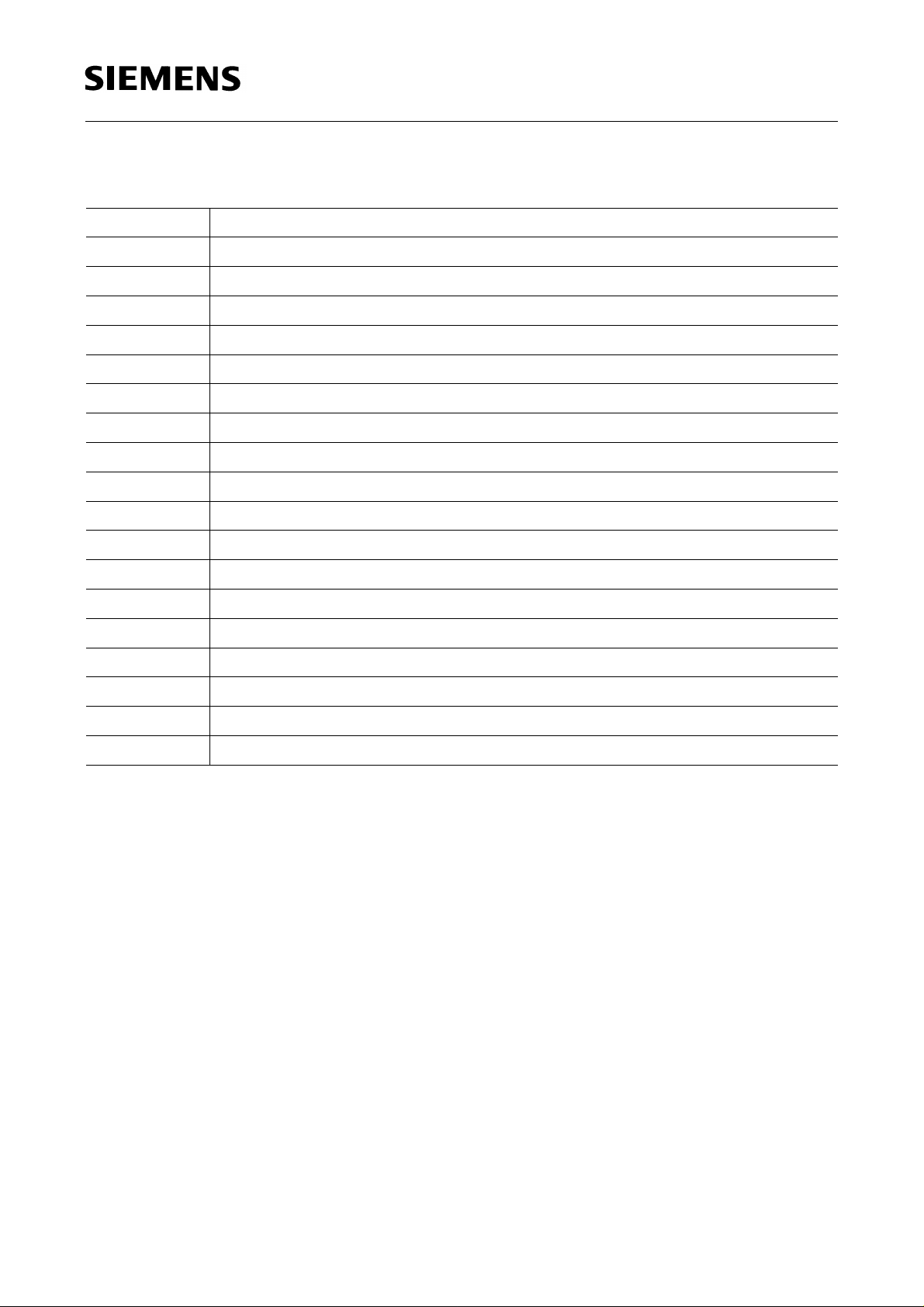
Pin No. Function
1 Video IF input
2 SCART switch A/W
3 SCART input
4 SCART input/output
TDA 5931-65
5+
6 Positive video output
7 Video output of the sound trap (2 Vpp)
8 Ground
9 Video input of the sound trap (3 Vpp)
10 Demodulator tank circuit
11 Demodulator tank circuit
12 TV-standard switch-over (B/G) – (L)
13 Low-pass filter (averaging)
14 Tuner AGC threshold
15 Tuner AGC output
16 AGC-time constant
17 Ground
18 Video IF input
V
supply voltage
S
Semiconductor Group 32
Page 3
TDA 5931-65
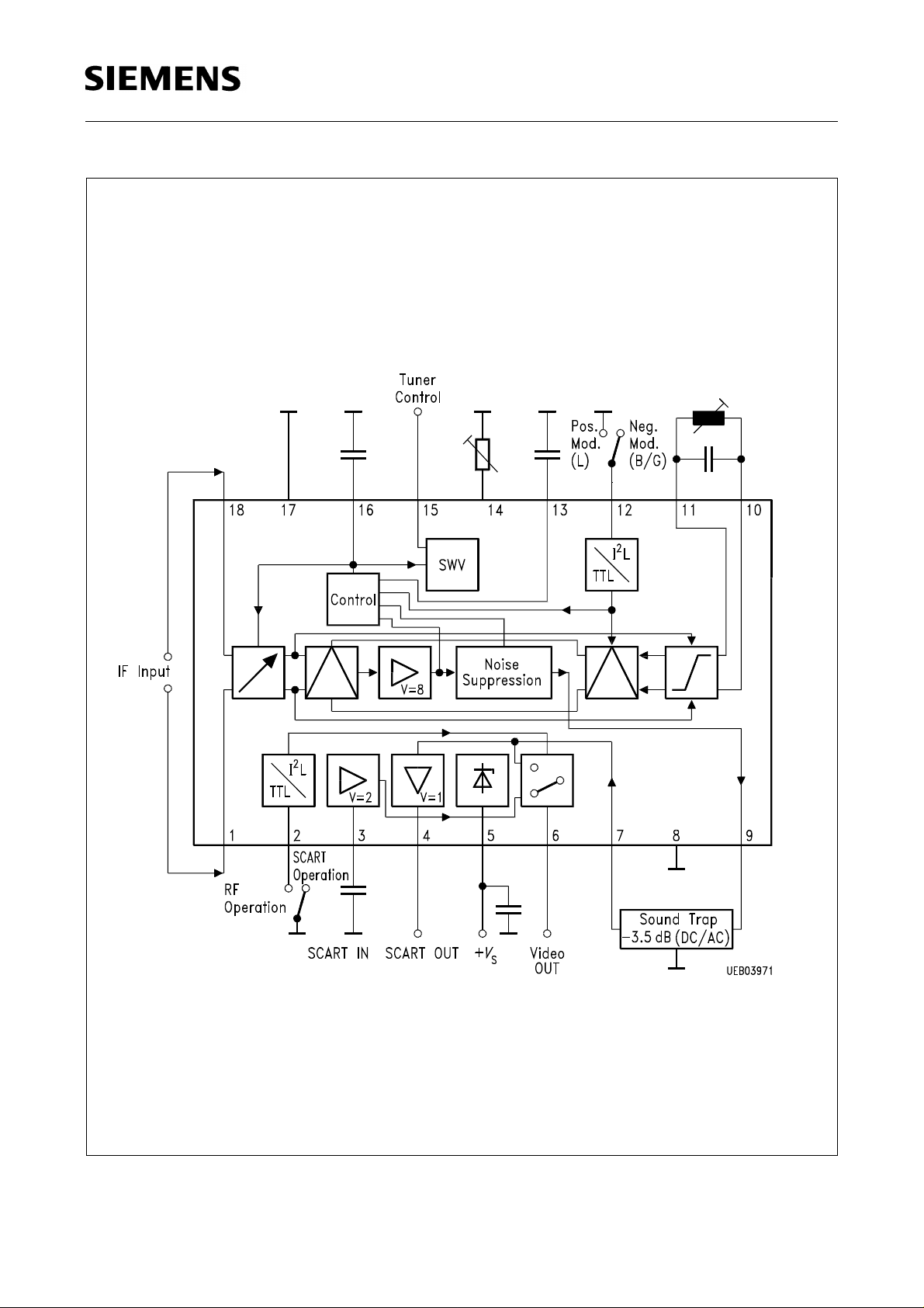
Block Diagram
Semiconductor Group 33
Page 4
TDA 5931-65
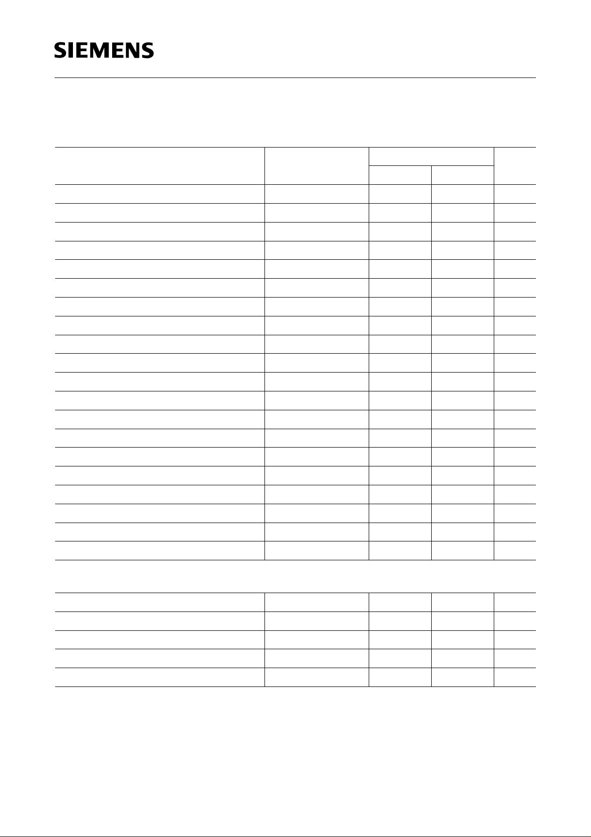
Absolute Maximum Ratings
T
= 0 to 70 °C
A
Parameter Symbol Limit Values Unit
min. max.
Sound trap input
Demodulator output
Demodulator output
Supply voltage
SCART A/W
Pos. video output
Pos. video output
Demodulator tank circuit
SCART OUT
SCART OUT
Tuner AGC threshold
Tuner AGC output
IF input
IF control
Norm switch-over
Norm switch-over
SCART IN
Junction temperature
Storage temperature
Thermal resistance (system-air)
V
7
V
9
I
9
V
5
V
2
I
6
V
6
V10/V
I
4
V
4
V
14
V
15
V1/V
V
16
V
12
V
13
V
3
T
j
T
stg
T
th SA
18
11
3.3 8.5 V
0 V
5
V
– 3 10 mA
0 13.2 V
06V
– 3 5 mA
0 8.5 V
0 V
5
V
– 3 5 mA
0 V
5
V
06V
010V
06V
0 8.5 V
06V
06V
06V
150 ˚C
– 40 125 ˚C
70 K/W
Operating Range
Supply voltage
Supply voltage delayed tuner AGC
Ambient temperature during operation
Input frequency range – 3 dB
Input frequency range – 0.3 dB
V
5
V
15
T
A
f
IF
f
IF
10.8 13.2 V
1.5 13.2 V
070˚C
10 100 MHz
30 75 MHz
All voltage values are referenced to ground, if not stated otherwise.
The current are identified according to the source/sink principle. If the IC considered a sink (the
current flows from the respective pin to ground), it is identified by a negative algebraic sign.
However, if the IC is the source (the current flows from VB via the respective pin to ground), it is
identified by a positive algebraic sign.
Semiconductor Group 34
Page 5
TDA 5931-65
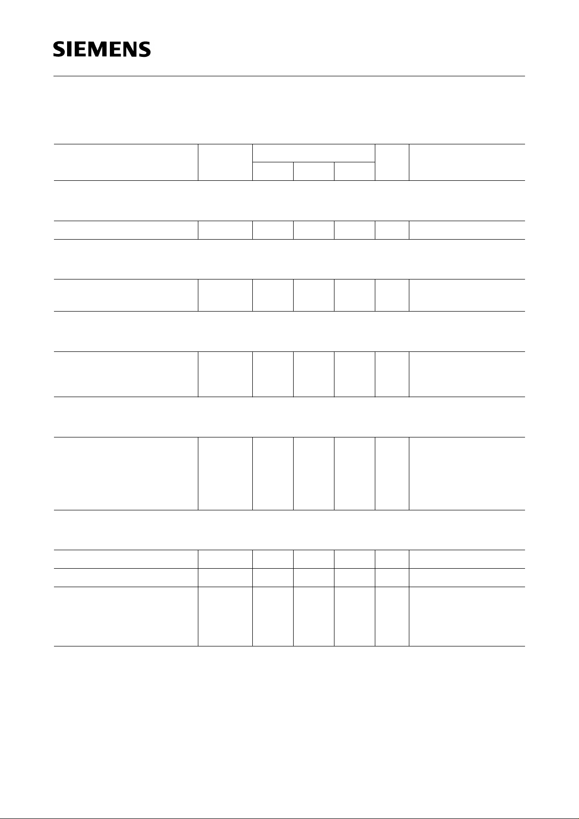
Characteristics
T
= 25 ˚C; VS = 12 V
A
Parameter Symbol Limit Values Unit Test Condition
min. typ. max.
Static Characteristics
Total current consumption –
I
5
38.5 56 71.5 mA V
AGC Voltage
Min. AGC
Max. AGC
V
16
V
16
0
2.6
AGC-Time Constant (by neg. modulation)
I
Charge current (
max
:2)
Discharge current
Charge/discharge ratio
I
16
– I
V
16
16
0.55
13
55
AGC-Time Constant (by pos. modulation)
Charge current
Discharge current
Discharge current
Charge/discharge ratio
I
16
– I
– I
V
16
16
16
1.1
0.15
70
4000
0.1
2.85
0.7
17
82
1.4
0.25
90
5600
0.5
6.0
0.95
23
140
1.7
0.35
110
9000
V
V
mA
µA
mA
µA
µA
= 10 mVrms
1/16
V
= 45 µVrms
1/16
V
= 175 mVrms
1/16
V
= 2 V; V6< 2.2 V
16
V
= 2 V; V6> 2.8 V
16
V
= 2 V; V6≥ 4.1 V
16
V
= 2 V;
16
3.1 V < V6 < 4.1 V
V
= 2 V; V6< 2.3 V
16
Averaging by Pos. Modulation
White level
Zero carrier level
Tuner AGC threshold
I
5
= I
max
:2
V
13
V
13
V
14
I
14
V
16
V
16
4.9 5.7 6.5 V V
3.3 3.7 4.1 V V
4.2
650
2.8
0.33
4.5
850
3.1
0.38
4.8
1050
3.4
0.43
V
µA
V
V
= 10 mVrms
1/18
= 0 V; V16 = 3 V
1/18
R
V
R
R
14/17
= 0 V
14
14/17
14/17
= ∞
= 10 kΩ
= 10 Ω
The characteristics data apply to the supply voltage range VS stated or in case of alignment to the
alignment instructions (see page 40). All static voltages are referenced to ground if not stated
otherwise.
The input levels are given as rms values referenced to synchronous peak fPC = 38.9 MHz.
Semiconductor Group 35
Page 6
TDA 5931-65
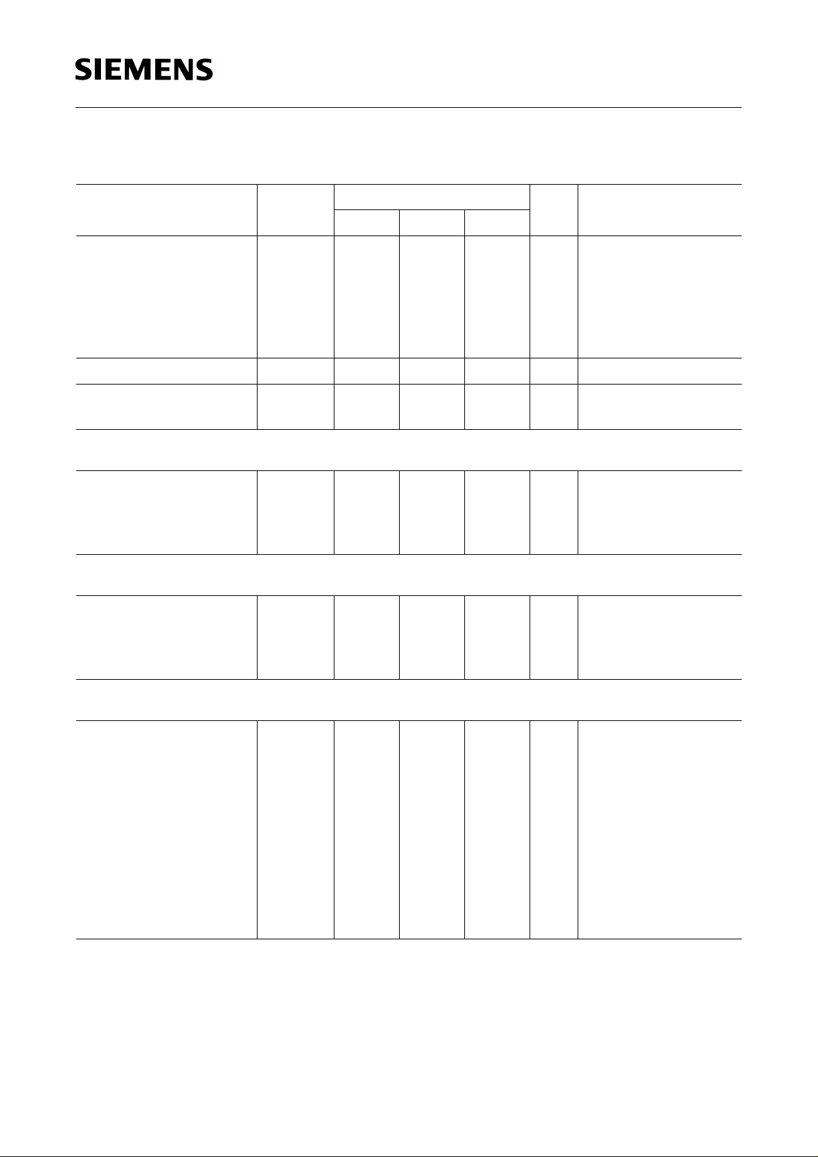
Characteristics (cont’d)
Parameter Symbol Limit Values Unit Test Condition
min. typ. max.
Tuner AGC current
–
max. 1 ms
– I
IF input
Demodulator tank
V
V
Video Output (Demodulator)
Output current
Output current
Sychron level
– I
I
9
V
Sound Trap Input
Sychron pulse level
White level
V
V
I
1
10
9
7
7
15
15
, V
, V
9
10
0
5.7 6.0 6.3 V
18
V
11
–
5
3.5
1.9
18
–
V
3.8
2.6
–
5
4
5.2
5.6
3.3 3.7
5.7 6.0
30
10
V
5
4.1
3.3
6.2
–
mA
µA
V
mA
mA
V
V
V
V
= 0.5 V
15
V
= 100 mVrms
1/18
V
= 0.75 V
14
V
= 0.5 V
15
V
= 10 mVrms
1/18
V
= 4.0 V
14
V
= 6 V, V
9
5
5
1, 18
=
carrier no-demod.
to ground
V
= 10 mVrms
1/18
Signal ratio V
Signal ratio V
V
= 0 V; V16 = 3 V
1/18
9/7
9/7
= 3/2
= 3/2
0 V > V2 > 2.4 V
Pos. Video Output
Output current
Pos. modulation
(L standard)
White level
Zero carrier (sync.)
Neg. modulation
(BG standard)
Synchron pulse level
Zero carrier
– I
I
6
V
V
V
V
6
1.7
4
2.2
2.7
mA
mA
V
= 6 V
6
to ground via
R = 500 Ω
see Sound Trap
Input
6
6
6
6
3.9
1.9
1.9
4.1
4.2
2.2
2.2
4.4
4.9
2.7
2.7
5.1
V
V
V
V
V
= 10 mVrms
1/18
V
= 0 V; V16 = 3 V
1/18
V
= 10 mVrms
1/18
V
= 0 V; V16 = 3 V
1/18
Semiconductor Group 36
Page 7
TDA 5931-65
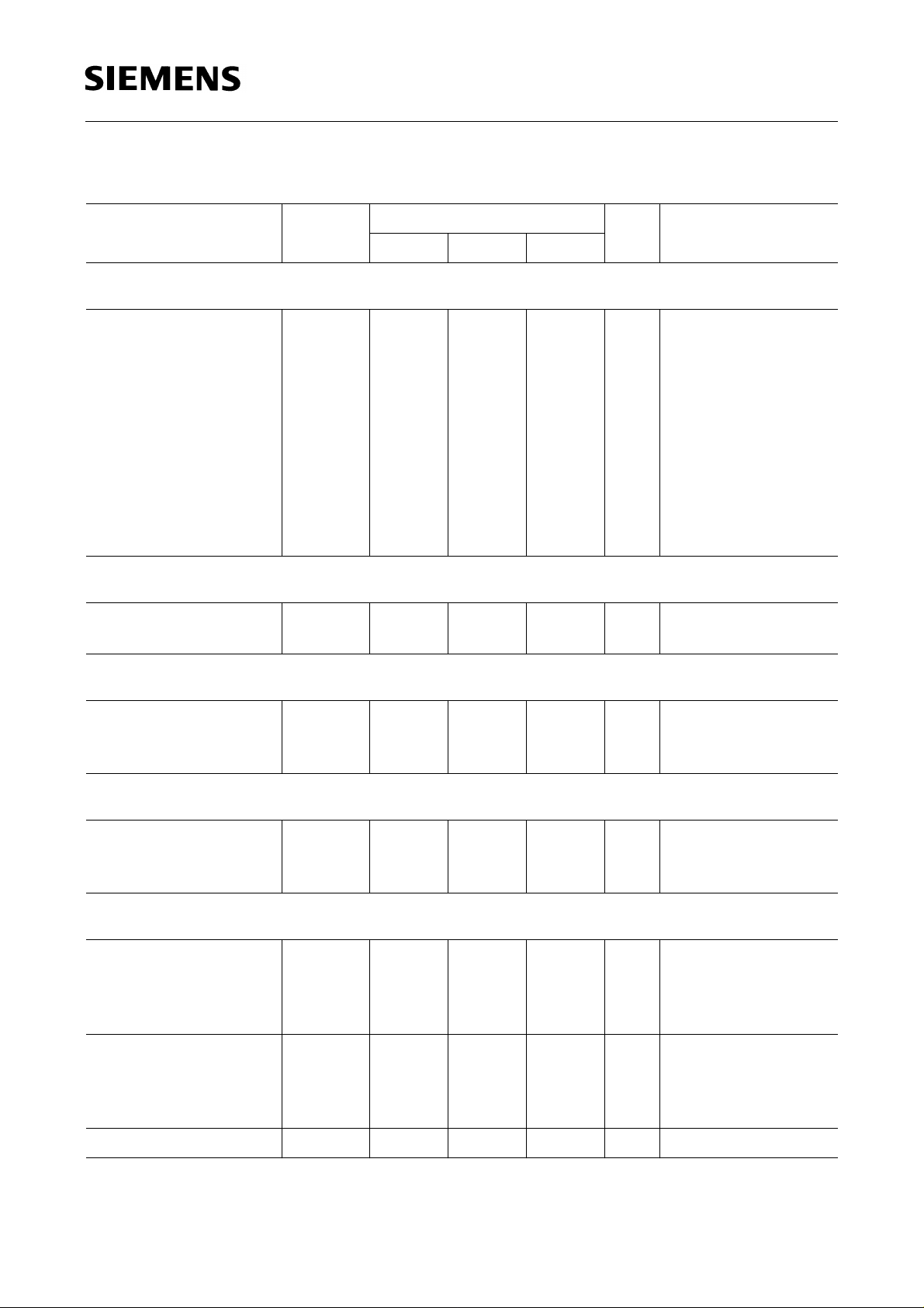
Characteristics (cont’d)
Parameter Symbol Limit Values Unit Test Condition
min. typ. max.
Neg. SCART Output
Output current
Pos. modulation
(L standard)
White level
Zero carrier (sync.)
Neg. modulation
(BG standard)
Synchron pulse level
Zero carrier
Pos. SCART Input 4
Clamp level
Output current
Switching Voltage
L = L/E standard
H = B/G standard
o. open
– I
I
4
V
V
V
V
V
I
3
V
V
4
4
4
4
3
12
12
4
1.6
2
2.6
mA
R
= ∞; see Sound
L
Trap Input
4
mA
V
= V
4
5
to ground via
R = 500 Ω
V
V
V
V
1.8
3
0
2.4
– 5.3
5
– 3.2
5
– 3.2
5
– 5.5
5
V
V
V
V
– 5.0
5
– 2.9
5
– 2.9
5
– 5.2
5
V
V
V
V
– 4.3
5
– 2.5
5
– 2.5
5
– 4.6
5
1.9 2 V
1.9
6
V
V
V
V
mA
V
V
V
= 10 mVrms
1/18
V
= 0 V; V16 = 3 V
1/18
V
= 10 mVrms
1/18
V
= 0 V; V16 = 3 V
1/18
via R = 270 kΩ at
ground V3 = 1.2 V
Switching Voltage
Open = SCART operat.
H = SCART operation
L = HF operation
V
2
V
2
V
2
2.4
0
Dynamic Characteristics
Min. IF-input voltage
start of internal
AGC operation
f
rms V
PC
1/18
45 60 µV 6 Vpp – 1 dB
Max. IF-input voltage
(end of internal
AGC-control range)
f
rms V
PC
IF-control range ∆
1/18
v 65 70 dB
105 140 mV 6 Vpp – 1 dB
Semiconductor Group 37
6
1.9
V
V
Page 8
TDA 5931-65
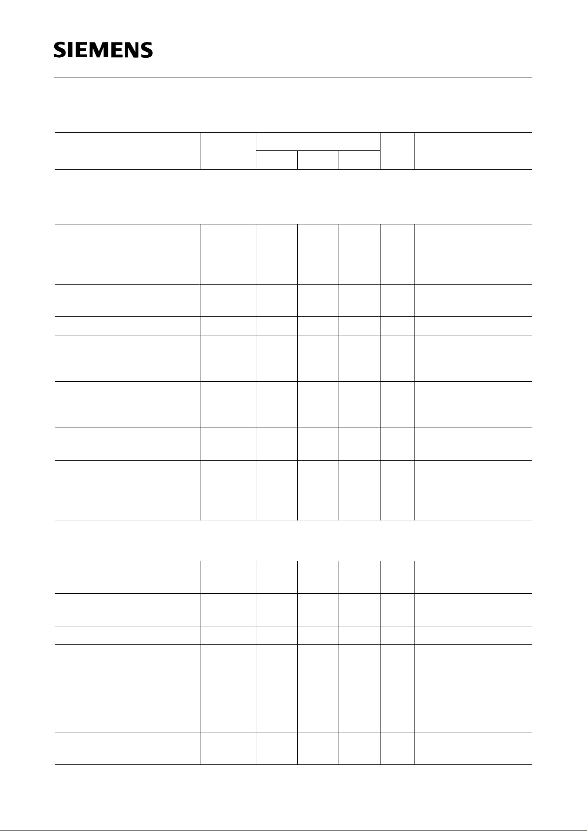
Characteristics (cont’d)
Parameter Symbol Limit Values Unit Test Condition
min. typ. max.
Video output voltages (peak to peak) fPC = 10 mVrms with neg. modulation and
residual carrier = 10%; with neg. modulation and residual carrier < 6%
Pos. video output
changes related to
TV-standard switch over
Change due to operating
voltage
Neg. SCART output
Changes of the video output
voltage over the control
range of 55 dB
Video gain
Video bandwidth
Cross talk attenuation
V
6
∆V
6
V
4
∆
V
6
V
6/V3
P
6/3-3dB
A
1.8 2.0
2
2.2
5
Vpp%0V <V2< 1.9 V
0V <V12< 1.9 V;
0 < V2 < 1.9 V
2.4 V < V12 < 6 V
1.5 3 % ∆
V
/∆V
6
5
10.8 V < V5 < 13.2 V
1.9 2.1 2.3 Vpp RL = ∞
0.2 0.5 dB
1.9 2.0 2.1 RG < 500 Ω;
2.4 < V2 < 6 V;
V
= 1 Vpp (2 MHz)
3
8 9 MHz 2.4 < V2 < 6 V;
V
= 1 Vpp sinus
3
40 50 dB 0 < V2 < 1.9 V;
V
= 0 V; V16 = 3 V;
1/18
V
= 1 Vpp sinus
3
50 Hz … 10 MHz
Design Notes (no 100% final test)
Input resistance
R
1/18
1.5 2 2.5 kΩ
(symmetrical)
Input capacitance
C
1/18
(symmetrical)
Low pass cut-off
f
– 3 dB (13)
70 100 130 Hz C
Pos. video output
white level
Synchron pulse level
V
6
V
6
3.9
1.9
frequency
Video input voltage
± 3 dB at
R
< 500 Ω
G
V
3
Semiconductor Group 38
25pF
2.4 < V2 = 6 V;
(SCART operation)
4.2
4.9
V
V
video signal
2.2
2.7
V
V
video signal
1 Vpp
= 100 nF ± 10%
13/17
= 1 Vpp norm
3
= 1 Vpp norm
3
Page 9
TDA 5931-65
Characteristics (cont’d)
Parameter Symbol Limit Values Unit Test Condition
min. typ. max.
Intercarrier noise voltages ratio (weighted according CCIR 468) with parallel tank circuit 38.9 MHz,
SAW 361 D, fTT = 5.5 MHz (– 13 dB), demod.: TBA 120
FuBk – test picture
FuBk – test picture
Dyn. Output Resistance
Pos. video output
Neg. video output
Noise figure
V
= – 57 dBm =
1/18
+ 50 dB µV
R
= 800 Ω
G
Video noise voltage ratio at
BT = 10 mVrms
0 dB = 700 mVrms BA
unweighted
weighted according to
CCIR Rec. 567-1
S/N
S/N
– ∆S/N
– ∆S/N
R
6
R
4
F
S/N
S/N
2
80
100
50
55
48
dB
V
FuBk mod.
17
dB
V
2.753 MHZ mod.
dB
with detuning
∆f = – 400 kHz
11
dB
with detuning
∆f = + 400 kHz
115
150
150
200
Ω
Ω
57dB
55
60
dB
dB
= 10 mVpp
1/18
= 10 mVpp
1/18
Video Frequency Response
– 3 dB
– 12 dB
B
3 dB
B
– 12 dB
8
15
Residual Carrier Voltage at Video Output
f
= 10 mVrms 38.9 MHz
PC
V
6
Fundamental wave
1. harmonic wave
V
6
f = 77.8 MHz
Semiconductor Group 39
10
17
3.0
0.3
13
20
6.0
0.6
MHz
MHz
mV
mV
Page 10
TDA 5931-65
Characteristics (cont’d)
Parameter Symbol Limit Values Unit Test Condition
min. typ. max.
Differential Gain with fPC = 10 mV (staircase signal)
Peak to Peak According to CCIR Rec. 567-1
Staircase signal
Changes via AGC
Changes via detuning
f
= 38.9 MHz;
PC
DG
∆DG / ∆v
∆DG / ∆f
∆f ± 400 kHz
Differential Phase with
f
= 10 mVrms (staircase signal)
PC
Peak to Peak According to CCIR Rec. 567-1
Staircase signal
Changes via AGC
Changes via detuning
f
= 38.9 MHz;
PC
DP
∆DP / ∆v
∆DP / ∆f
∆f ± 400 kHz
Interdemodulation Ratio
With fIM = 1.07 MHz = fTT – f
FT
With BT = 10 mVeff
With sound porch – 13 dB
With sound porch – 13 dB
With sound porch – 13 dB
a
IM
a
IM
a
IM
32
54
51
4.5 6
± 1
± 1.5
2 2.5
1
± 1
38
60
57
–
–
–
%
%
%
degree
degree
degree
dB
dB
dB
OFW G 3950
OFW 361D
OFW G 1956
Demodulator Tank Circuit Voltage
f
= 38.9 MHz; C = 47 pF
PC
L = 350 nH
V
10/11
300 450 600 mVpp
100 ≤ Q0≤ 120;Q8≈ 60;
B ≈ 0.8 … 1.0 MHz
Synchron pulse ∆
Semiconductor Group 40
V
Sync/V6
5%
Page 11

Alignment Instructions
TDA 5931-65
At a video carrier input level of V
of V16 = 1.5 V the tank circuit is aligned that way, that at the positive video output the demodulated
video signal 6 Vpp is at its maximum.
As a modulation every sufficient video test pattern can be used. Then the superimposed AGCcontrol voltage at pin 16 is reduced until the video signal has an amplitude of approx. 2 Vpp. The
video signal is then fine tuned for its maximum.
The adjustment is not critical due to the wide maximum.
The adjustment can also be performed regarding intercarrier signal to noise ratio, differential gain or
2T-pulse response.
= 4 mVrms, fPC = 38.9 MHz and a superimposed AGC voltage
1/18
Semiconductor Group 41
Page 12
TDA 5931-65
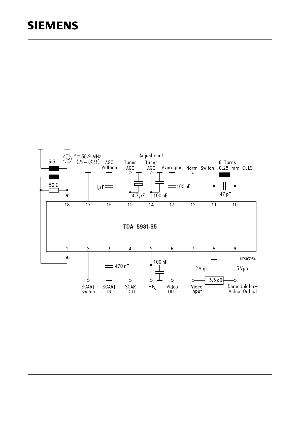
Test Circuit
Semiconductor Group 42
Page 13
TDA 5931-65
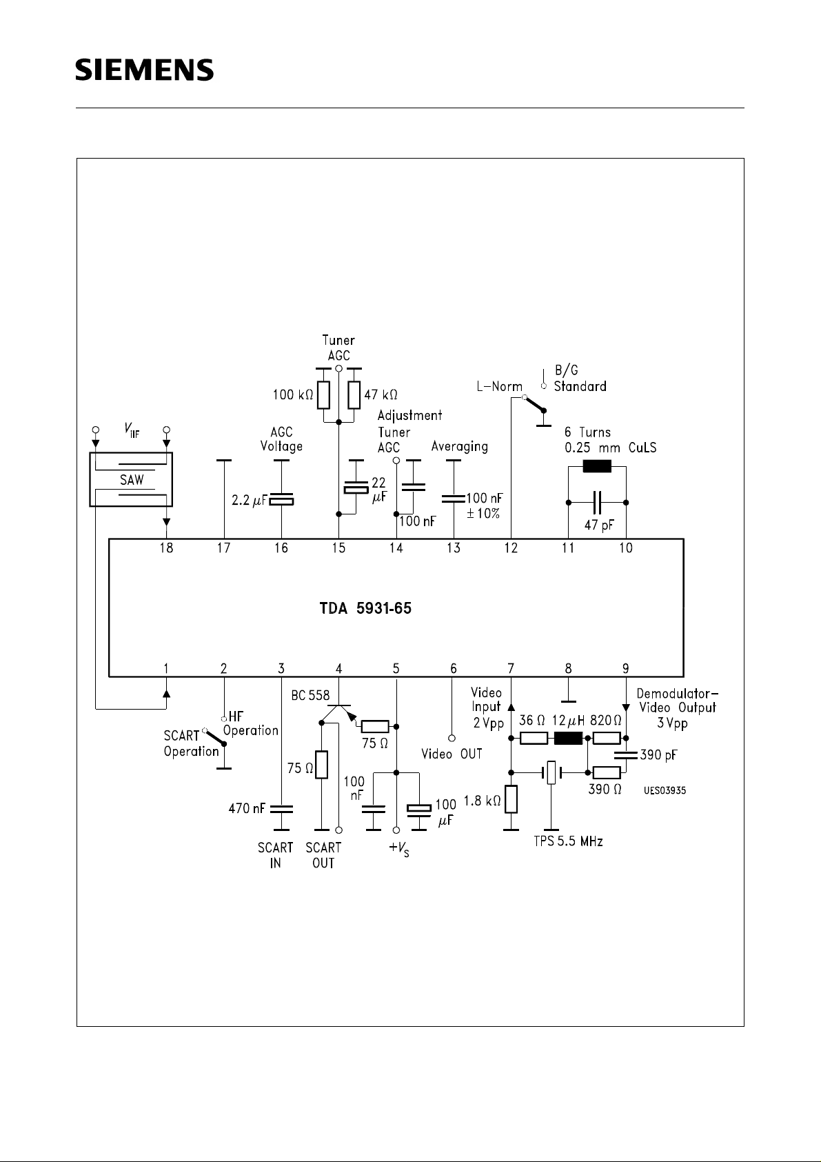
Application Circuit
Semiconductor Group 43
 Loading...