

Page 1
Page 2
Page 3
Page 4
Page 5
Philips Semiconductors Product specification
TDA5240TBrushless DC motor drive circuit
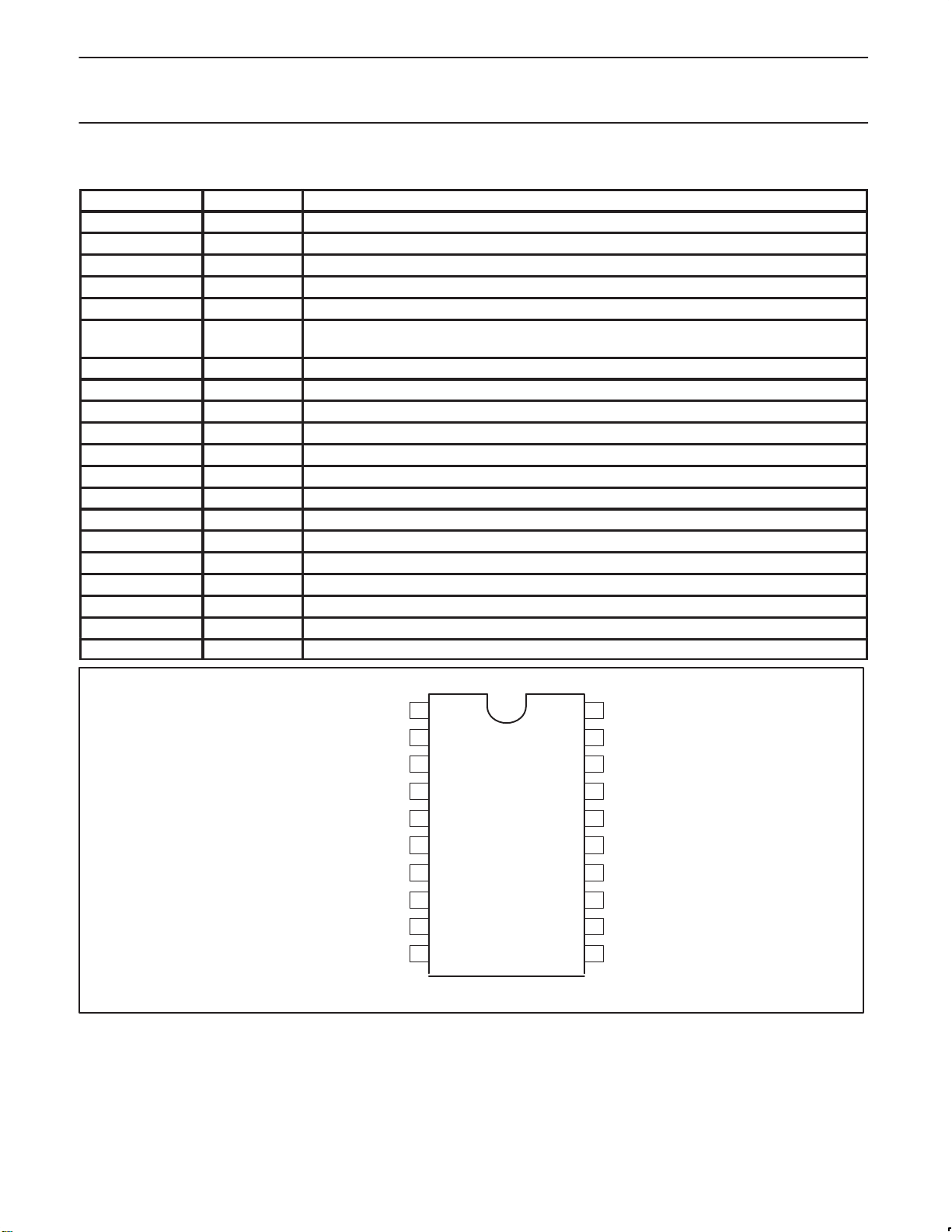
PINNING
SYMBOL PIN DESCRIPTION
GND1 1 ground (0 V) motor supply return for output stages
n.c. 2 not connected
MOT2 3 driver output 2
n.c. 4 not connected
V
P
PGIN 6 position generator: input from the position detector sensor to the position detector
FGPG 7 FG/PG (open collector)
GND2 8 ground supply return for control circuits
PGOUT 9 position generator output of the position detector stage
CAP–CDM 10 external capacitor connection for commutation delay timing
CAP–CDS 11 external capacitor connection for commutation delay timing copy
CAP–ST 12 external capacitor connection for start–up oscillator
CAP–TI 13 external capacitor connection for timing
CTL IN 14 non–inverting input of the control amplifier
MOT0 15 input from the start point of the motor coils
CAP–CPC 16 external capacitor for stability of control loop
n.c. 17 not connected
MOT3 18 driver output 3
n.c. 19 not connected
MOT1 20 driver output 1
5 positive supply voltage
stage (optional)
GND1
n.c.
MOT2
NC
PGIN
FGPG
GND2
PGOUT
CAP–CDM
1
2
3
4
V
5
P
6
7
8
9
10 11
TDA5240T
Fig. 3 Pin configuration
20
19
18
17
16
15
14
13
12
MOT1
n.c.
MOT3
n.c.
CAP–CPC
MOT0
CTL IN
CAP–TI
CAP–ST
CAP–CDS
November 96
5/19
Page 6
Page 7

Philips Semiconductors Product specification
TDA5240TBrushless DC motor drive circuit
CHARACTERISTICS
VP = 14.5 V "10%; T
Symbol
Supply
V
P
I
P
Thermal protection
T
SD
DT
MOT0 – CENTER TAP
V
I
I
I
V
CSW
DV
CS
V
H
MOT1, MOT2 AND MOT3
V
DO
DV
OL
DV
OH
I
LIM
T
r
T
f
V
DHF
V
DLF
I
DM
CTL IN
V
CTLIN
V
CTLIN0
G
TRAN
= –10 °C to 70 °C, unless otherwise specified
amb
Parameter Conditions Min Typ Max Unit
Supply voltage range note 1 4 – 18 V
Input current range note 2 – 5.3 7 mA
Local temperature at temperature
130 140 150 °C
sensor causing shut–down
Reduction in temperature
after shut–down – TSD–30 – °C
before switch–on
Input voltage range –0.5 – V
Input bias current 0.5 V<VI <VP–1.5 V –10 – –
P
V
mA
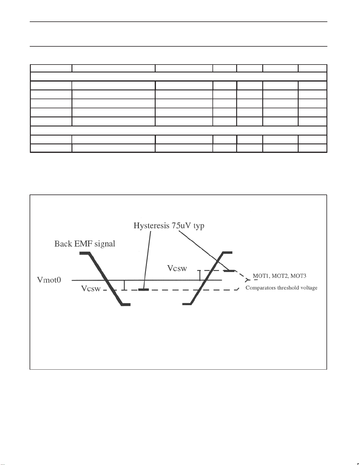
Comparator Switching Level note 3 20 30 40 mV
Variations in comparator switching
–3 0 +3 mV
levels
Comparator input hysteresis – 75 –
mV
Voltage drop at 25 °C IO = 100 mA – 0.93 1.05 V
(V
upper stage + V
out
Variation in voltage between lower
transistors
Variation in voltage between upper
transistors
Current limiting
Rise time switching output between
1.9 and 12.2 V
Fall time switching output between
lower stage) IO = 500 mA – 1.65 1.9 V
out
in control mode;
= 100 mA
I
O
in control mode;
I
= –100 mA
O
12 V/6.8W
I
= 250 mA 7 12 17
O
– – 150 mV
– – 150 mV
0.6 0.85 1 A
IO = 250 mA 16 23 30
ms
ms
12.2 and 1.9 V
Diode forward voltage (DH) notes 4 and 5; see Fig. 2;
= –500 mA
I
O
Diode forward voltage (DL) notes 4 and 5; see Fig. 2;
I
= 500 mA
O
– – 1.5 V
–1.5 – – V
Peak diode current note 5 – – 1 A
Input voltage range 0 – V
Offset voltage See Fig. 6
V
CAPCPC
v 1.1 V
Transfer gain CAP–CPC = 100 nF
= 1.5V and
V
CTLIN
V
= 3 V
CTLIN
0.7 – – V
4.5 5 5.5 V/V
P
V
November 96
7/19
Page 8
Philips Semiconductors Product specification
TDA5240TBrushless DC motor drive circuit
Symbol UnitMaxTypMinConditionsParameter
PG IN
V
I
I
B
R
I
V
CSW
+/–V
IAMP
PG OUT (open collector)
V
OL
V
OHmax
t
THL
t
PL
FG/PG (open collector)
V
OL
V
OHmax
t
THL
d
t
PL
CAP–ST
I
I
I
O
V
SWL
V
SWM
V
SWH
CAP–TI
I
I
I
OH
I
OL
V
SWL
V
SWM
V
SWH
CAP–CDM
I
I
I
O
II/I
O
V
IL
V
IH
Input voltage range –0.3 – +5 V
Input bias current – – 650 nA
Input resistance 5 – 30
kW
Comparator switching level 86 93 107 mV
Comparator input hysteresis – 8 – mV
Output voltage LOW IO = 1.6 mA – – 0.4 V
Output voltage HIGH – – V
Transition time HIGH-to-LOW;
– 0.5 –
P
V
ms
CL = 50 pF;
RL = 10 kW
Pulse width LOW 4 – 10
ms
Output voltage LOW IO =1.6 mA – – 0.4 V
Maximum output voltage HIGH – – V
Transition time HIGH–to–LOW
– 0.5 –
P
V
ms
CL = 50 pF
RL = 10 kW
Ratio of FG frequency and
– 1:2 – –
commutation frequency
Duty factor – 50 – %
Pulse width LOW after a PG IN pulse 5 7 15
Output sink current 1.5 2.0 2.5
Output source current –2.5 –2.0 –1.5
ms
mA
mA
Lower switching level – 0.20 – V
Middle switching level – 0.30 – V
Upper switching level – 2.20 – V
Output sink current 22 30 38
Output source current HIGH –70 –63 –56
Lower source current LOW –6.0 –5.3 –4.6
mA
mA
mA
Lower switching level – 50 – mV
Middle switching level – 0.30 – V
Upper switching level – 2.20 – V
Output sink current 10.6 16.2 22
Output source current –5.3 –8.1 –11
mA
mA
Ratio of sink to source current 1.85 2.05 2.25
Input voltage level LOW 780 860 940 mV
Input voltage level HIGH 2.3 2.4 2.55 V
November 96
8/19
Page 9
Philips Semiconductors Product specification
TDA5240TBrushless DC motor drive circuit
Symbol UnitMaxTypMinConditionsParameter
CAP–CDS
I
I
I
O
II/I
O
V
IL
V
IH
CAP–CPC
I
I
I
O
NOTES:
1. An unstabilized supply can be used; transients of 2 V allowed with max slope 0.1 V/s.
2. All other inputs at 0 V; all outputs at V
3. Switching levels with respect to MOT1, MOT2 and MOT3.
4. Drivers are in high impedance OFF–state.
5. The outputs are short–circuit protected by limiting the current and the IC temperature.
Output sink current 10.1 15.5 20.9
Output source current –20.9 –15.5 –10.1
A
A
Ratio of sink to source current 0.9 1.025 1.15
Input voltage level LOW 780 860 940 mV
Input voltage level HIGH 2.3 2.4 2.55 V
Output sink current 1 – 3 mA
Output source current –100 – –30
and IO = 0 A.
P
A
November 96
Fig. 4 Switching levels
9/19
Page 10

Philips Semiconductors Product specification
TDA5240TBrushless DC motor drive circuit
APPLICATION INFORMATION
Introduction
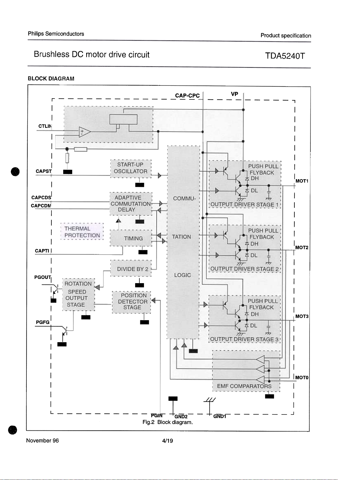
Figure 5 shows full–wave driving of a three phase motor requires three push–pull output stages. In each of the six possible states two outputs
are active, one sourcing and one sinking current. The third output presents a high impedance to the motor which enables measurement of the
motor EMF in the corresponding motor coil by the EMF comparator at each output. The commutation logic is responsible for control of the
output transistors and selection of the correct EMF comparator.
The zero–crossing in the motor EMF (detected by the comparator selected by the commutation logic) is used to calculate the correct moment
for the next commutation, that is, the change to the next output state. The delay is calculated (depending on the motor loading) by the adaptive
commutation delay block.
Because of high inductive loading the output stages contain flyback diodes. The output stages are also protected by a current limiting circuit and
by thermal protection of the six output transistors.
The zero–crossings can be used to provide speed information such as the tacho signal FG. A VCR scanner also requires a PG phase sensor.
This circuit has an interface for a simple pick–up coil. A multiplexer circuit is also provided to combine the FG and PG signals in time. The
TDA5240 is providing 1 multiplexed FG PG signal: pin7 (SO20) FG–PG 3 times the number of pole pairs. A PG output signal is generated;
pulse width is typically 7 µs.
Table 1 OUTPUT STA TES
ST ATE MOT1 MOT2 MOT3
1 Z L H
2 H L Z
3 H Z L
4 Z H L
5 L H Z
6 L Z H
In Table 1, the sequence of the six possible states of the outputs has been depicted
November 96
10/19
Page 11

Page 12
Page 13
Page 14
Page 15
Page 16
Page 17
Page 18

Page 19

Philips Semiconductors Product specification
TDA5240TBrushless DC motor drive circuit
Data sheet status
Product
Data sheet status
Objective
specification
Preliminary
specification
Product
specification
[1] Please consult the most recently issued data sheet before initiating or completing a design.
[2] The product status of the device(s) described in this data sheet may have changed since this data sheet was published. The latest information is available on the Internet at URL
http://www.semiconductors.philips.com.
[1]
status
Development
Qualification
Production
[2]
Definitions
Short-form specification — The data in a short-form specification is extracted from a full data sheet with the same type number and title. For
detailed information see the relevant data sheet or data handbook.
Limiting values definition — Limiting values given are in accordance with the Absolute Maximum Rating System (IEC 60134). Stress above one
or more of the limiting values may cause permanent damage to the device. These are stress ratings only and operation of the device at these or
at any other conditions above those given in the Characteristics sections of the specification is not implied. Exposure to limiting values for extended
periods may affect device reliability.
Application information — Applications that are described herein for any of these products are for illustrative purposes only. Philips
Semiconductors make no representation or warranty that such applications will be suitable for the specified use without further testing or
modification.
Disclaimers
Life support — These products are not designed for use in life support appliances, devices or systems where malfunction of these products can
reasonably be expected to result in personal injury . Philips Semiconductors customers using or selling these products for use in such applications
do so at their own risk and agree to fully indemnify Philips Semiconductors for any damages resulting from such application.
Right to make changes — Philips Semiconductors reserves the right to make changes, without notice, in the products, including circuits, standard
cells, and/or software, described or contained herein in order to improve design and/or performance. Philips Semiconductors assumes no
responsibility or liability for the use of any of these products, conveys no license or title under any patent, copyright, or mask work right to these
products, and makes no representations or warranties that these products are free from patent, copyright, or mask work right infringement, unless
otherwise specified.
Contact information
For additional information please visit
http://www.semiconductors.philips.com . Fax: +31 40 27 24825
For sales offices addresses send e-mail to:
Definitions
This data sheet contains data from the objective specification for product development.
Philips Semiconductors reserves the right to change the specification in any manner without notice.
This data sheet contains data from the preliminary specification. Supplementary data will be
published at a later date. Philips Semiconductors reserves the right to change the specification
without notice, in order to improve the design and supply the best possible product.
This data sheet contains data from the product specification. Philips Semiconductors reserves the
right to make changes at any time in order to improve the design, manufacturing and supply.
Changes will be communicated according to the Customer Product/Process Change Notification
(CPCN) procedure SNW-SQ-650A.
Koninklijke Philips Electronics N.V. 1996
All rights reserved. Printed in U.S.A.
Date of release: 11-96
Document order number: 9397 750 08756
yyyy mmm dd
1
 Loading...