

Page 1
Video and Sound IF with FM-PLL
Demodulator, AFC and V & S SCART
Features
● Features video and sound IF
● Video and sound SCART
● AFC
● NTSC option
TDA 5950X
Bipolar IC
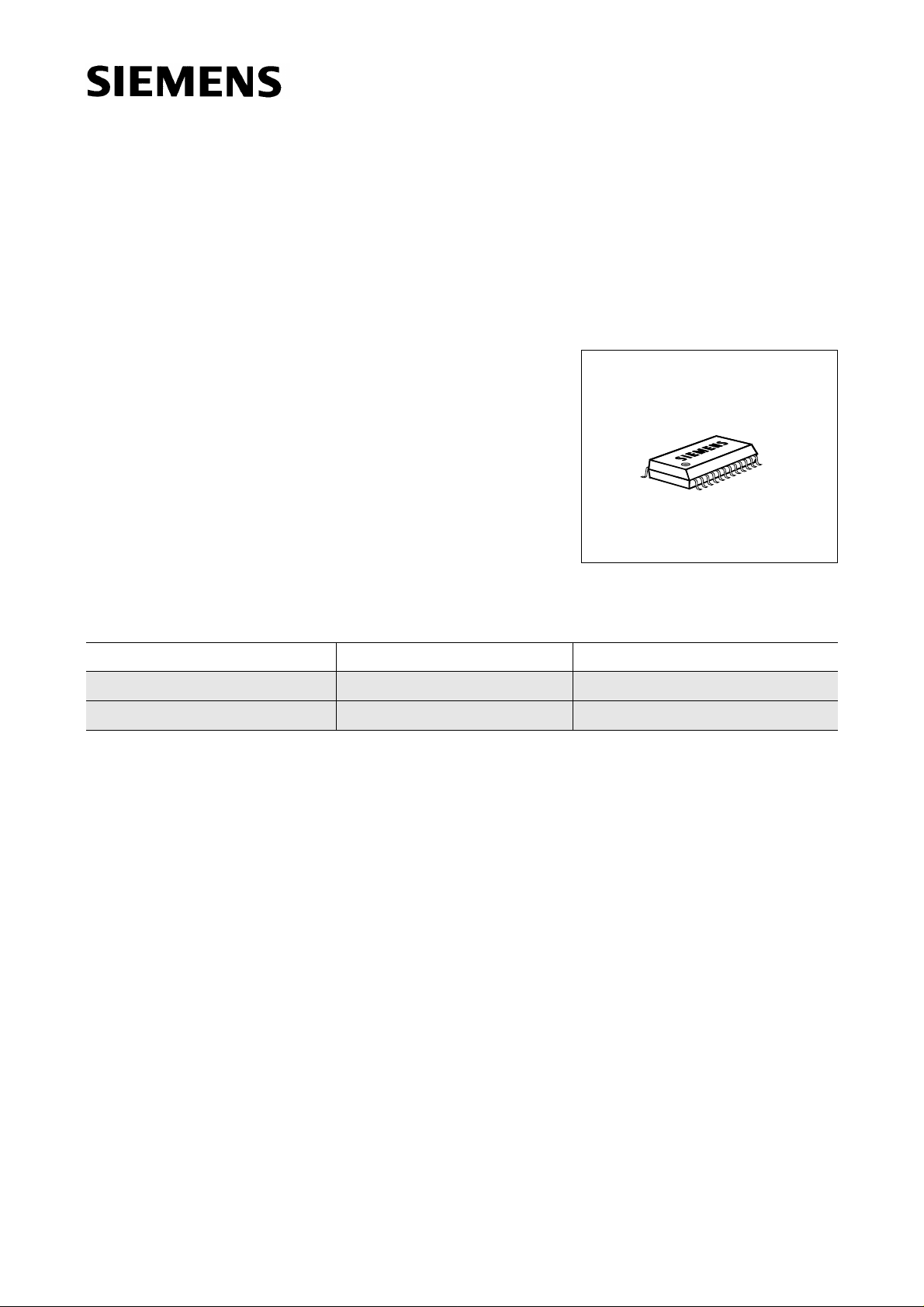
P-DSO-24-1
Type Ordering Code Package
TDA 5950X Q67000-A5112 P-DSO-24-1 (SMD)
TDA 5950X Q67007-A5112 P-DSO-24-1 Tape and Reel dry
Functional Description
Video IF Section
Video IF-broadband amplifier followed by a quasi-synchronous demodulator for negative
modulated IF signals. A video switch interface is included in the video section. A separate video
output after the demodulator permits the installation of one or more sound traps at the input of the
video switch. The tuner AGC threshold is set by means of a potentiometer, all other functions can
switched with open collector transistors.
Sound IF Section
FM-IF limiter with FM-PLL demodulator for the frequency range of 5.5 MHz to 6.5 MHz. The AF
section includes an audio switch followed by an audio buffer output.
Application
The TDA 5950X is suitable for application in television receivers or video tape recorders with A/V
switches.
Semiconductor Group 1 12.94
Page 2
TDA 5950X
Circuit Description
Video IF Section
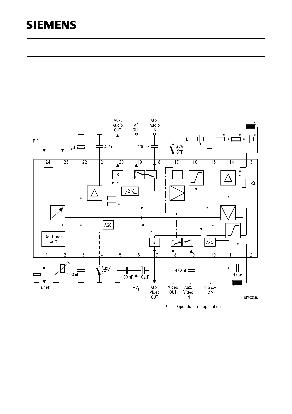
The video IF section incorporates a four-stage, capacitively coupled, symmetrical and controlled
amplifier, a limiter with selection and a mixer for quasi-synchronous demodulation of negative
modulated IF signals followed by a video output amplifier. The video demodulator output and the
video switch input are connected by means of a sound trap. The video switch has two inputs (for
signals from video demodulator and from external source) and two outputs. Parallel to the video
output amplifier the video signal is used for generating the AGC voltage. The control circuit is
designed on the integralaction AGC principle, employing a noise-free peak value detector. A
delayed tuner AGC voltage with positive control direction is derived from the AGC voltage via a
threshold amplifier that is set by means of an external potentiometer. An AFC push pull output
current is generated from picture carrier tank circuit.
Sound IF Section
The sound IF section incorporates a five-stage, symmetrical limiter amplifier followed by a PLL
demodulator. The AF section contains an audio switch followed by an output buffer.
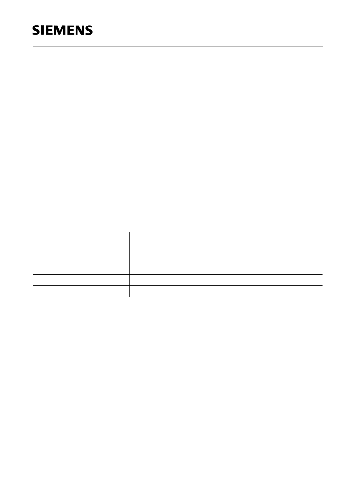
Switch Matrix
AUX/RF-Control
(Pin 4)
0 0 muted
01IF
1 0 muted
1 1 SCART
AV-OFF
(Pin 17)
Output
(Pin 8 / Pin 19)
Semiconductor Group 2
Page 3
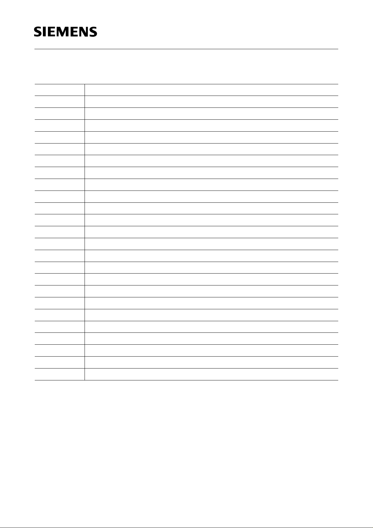
Pin Functions
Pin No. Function
1 Delayed tuner AGC output
2 Delayed tuner AGC threshold
3 AGC-time constant
4 Aux / RF control
5 Ground
TDA 5950X
6+
7 Auxiliary video output
8 Video output
9 Auxiliary video input
10 AFC output
11 Demodulator tank circuit
12 Demodulator tank circuit
13 Video input at sound trap output
14 Video demodulator output
15 Sound IF ground
16 Sound IF input
17 A / V OFF
18 Auxiliary audio input
19 Audio output
20 Auxiliary audio output
21 De-emphasis capacitor
V
supply voltage
S
22 Low-pass capacitor
23 Video IF input
24 Video IF input
Semiconductor Group 3
Page 4
TDA 5950X
Block Diagram
Semiconductor Group 4
Page 5
TDA 5950X
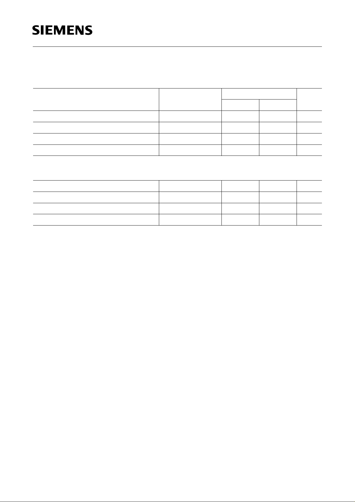
Absolute Maximum Ratings
T
= 0 to 70 ˚C
A
Parameter Symbol Limit Values Unit
min. max.
Supply voltage V
Junction temperature
Storage temperature
Thermal resistance
Operating Range
Supply voltage
Supply voltage delayed tuner AGC
Ambient temperature during operation
Input frequency range
T
T
R
V
V
T
f
IF
6
j
stg
th JA
6
1
A
08V
0 150 ˚C
– 40 125 ˚C
70 K/W
4.5 8 V
1 13.2 V
070˚C
12 80 MHz
Semiconductor Group 5
Page 6
TDA 5950X
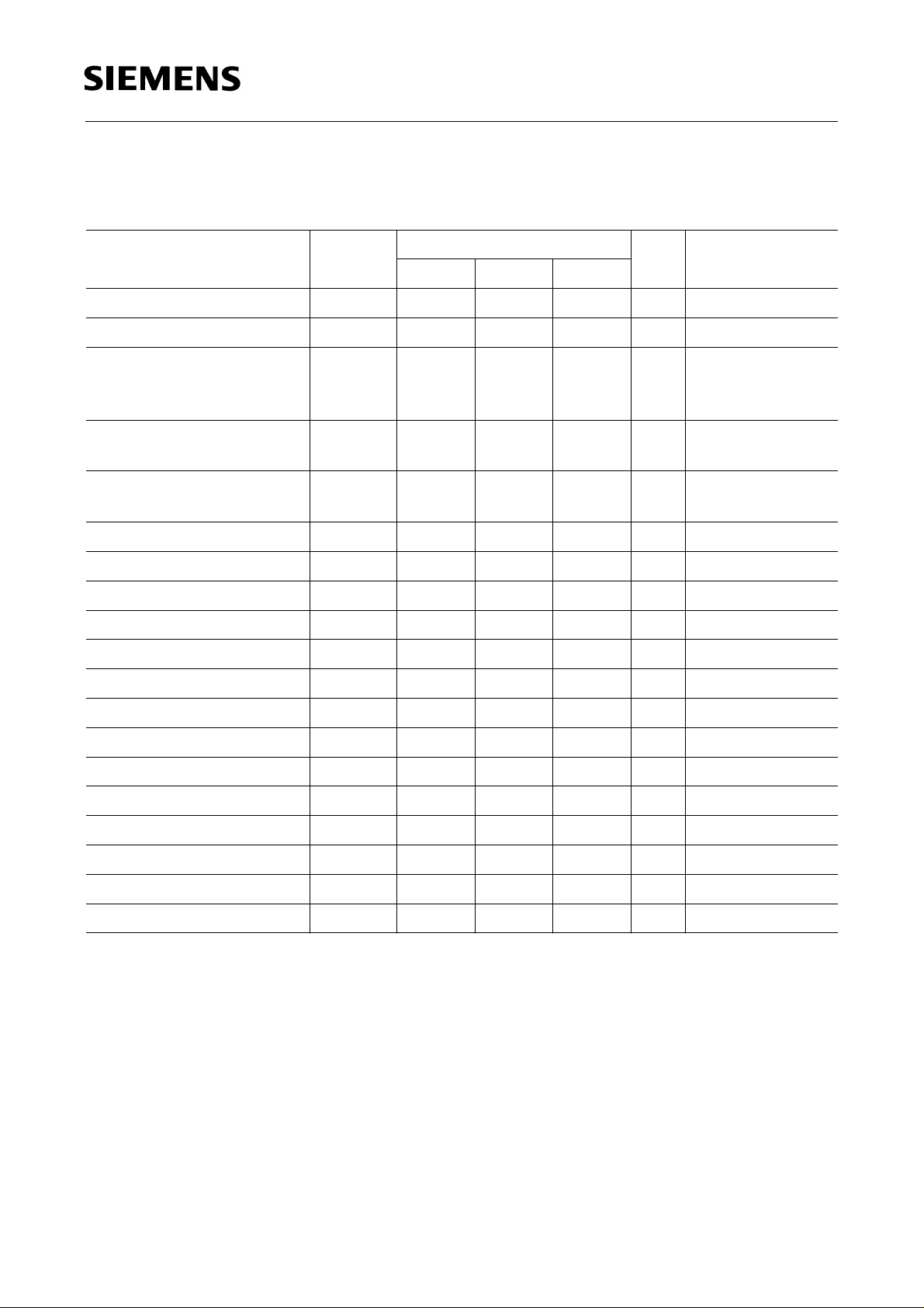
DC Characteristics
T
= 0 to 70 ˚C; VS = 5.0 V
A
Parameter Symbol Limit Values Unit Test Condition
min. typ. max.
Total current I
DC voltage; pin 1
Aux/RF switch; pin 4
H/open = Aux
L = RF
Sync tip level; pin 7
Sync tip level; pin 8
Sync tip level; pin 9
DC voltage; pin 10
DC voltage; pin 11
DC voltage; pin 12
Sync tip level; pin 13
Sync tip level; pin 14
DC voltage; pin 16
DC voltage; pin 18
DC voltage; pin 19
DC voltage; pin 20
DC voltage; pin 21
DC voltage; pin 22
DC voltage; pin 23
DC voltage; pin 24
6
V
1
V
4
V
4
V
7
47 55 63 mA
12 V
2.4
0
5.5
1.5
V
V
1.35 1.5 1.65 V RL≥ 2.7 kΩ||
10 pF
V
8
1.35 1.5 1.65 V RL≥ 2.7 kΩ||
10 pF
V
9
V
10
V
11
V
12
V
13
V
14
V
16
V
18
V
19
V
20
V
21
V
22
V
23
V
24
1.35 1.5 1.65 V
0.4 V6 – 0.4 V
V
– 1.3 V
6
V
– 1.3 V
6
1.35 1.5 1.65 V
1.15 1.3 1.45 V
0V
1.6 2 2.4 V
1.6 2 2.4 V
1.6 2 2.4 V
1.6 2 2.4 V
2.2 V
3.6 V
3.6 V
Semiconductor Group 6
Page 7
TDA 5950X
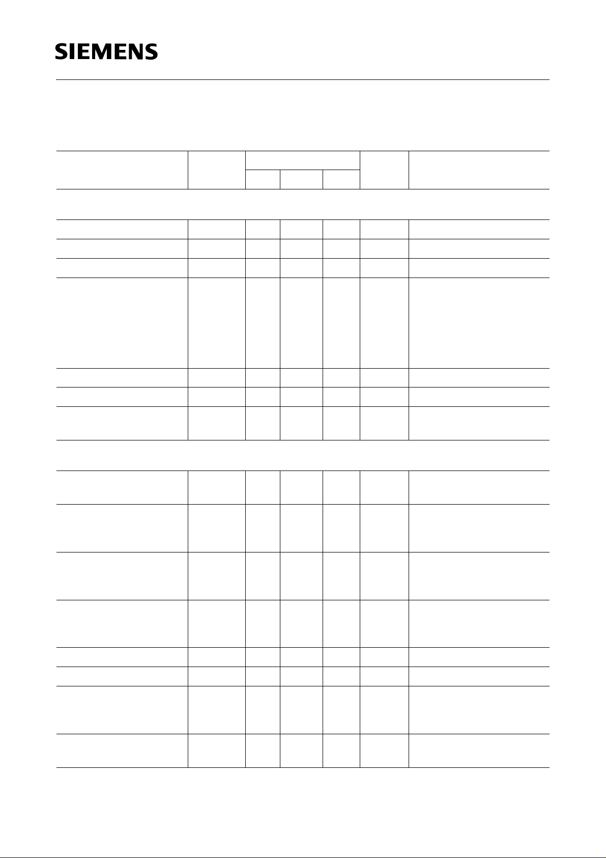
AC Characteristics
T
= 0 to 70 ˚C; VS = 5.0 V
A
Parameter Symbol Limit Values Unit Test Condition
min. typ. max.
Video IF Section
IF-input sensitivity
Max. IF-input voltage
IF-control range ∆
Video demodulator
output voltage
– 3 dB video bandwidth
Output impedance
Output sink current
Output source current
Sound IF Section
Min. sound IF-input
voltage (min. control)
AF-output voltage
Aux. AF-output voltage
Total harmonic distortion
Max. aux. input voltage
Gain audio switch
AM-Suppression
Signal to noise
ratio (weighted)
V
23/24
V
23/24
V
IF
V
14pp
B
14
R
14
I
14
I
14
V
16
V
19
V
20
THD
V
18rms
G
18-19
α
AM19/20
S/N
19/20
AFo
70 100 µV V
100 140 mV V
Video
Video
– 3 dB
+ 3 dB
60 66 72 dB
1.35 1.5
3.6
3.0
1.1
1.3
1.65 V
V
= 10 mV
IF IN
V
V
V
V
upper video clipping
zero carrier level
lower video clipping
sync tip level
8 10 MHz CL < 20 pF, RL > 1 kΩ
10 Ω
2
– 3
mA
mA
DC and AC
DC and AC
70 100 µV
175 250 350 mV ∆f = 30 kHz
f
= 1 kHz
mod
F
= 5.5 MHz…6.5 MHz
SIF
350 500 700 mV ∆f = 30 kHz
f
= 1 kHz
mod
F
= 5.5 MHz…6.5 MHz
SIF
0.2 0.3 % ∆f = 30 kHz
f
= 1 kHz
mod
F
= 5.5 MHz…6.5 MHz
SIF
1V
1
f
= 1 kHz
mod
m = 30 %
50 55 dB
50
60
55
65
dB
dB
V
= 1 mV…100 mV
16
V
= 500 µV…1 mV
16
V
= 1 mV…100 mV
16
Semiconductor Group 7
Page 8
TDA 5950X
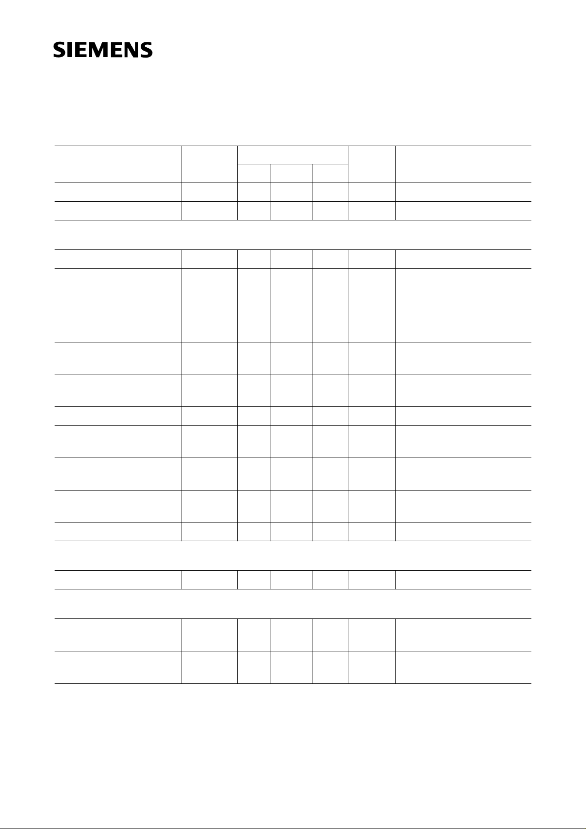
AC Characteristics (cont’d)
T
= 0 to 70 ˚C; VS = 5.0 V
A
Parameter Symbol Limit Values Unit Test Condition
min. typ. max.
Ripple rejection RR
Input impedance
Z
18
SCART-SWITCH
Input impedance Z
13
Gain of Video switch
Aux.
V
-video output
IN
VideoIN-aux. output
VideoIN-video output
f
= 5 MHz
mod
– 3 dB video bandwidth
– 3 dB video bandwidth
Cross talk attenuation
f
= 5 MHz
mod
Intermodulation
G
G
G
B
B
a
α
9-8
Suppression of video
signal harmonics
Signal to noise ratio
S/N
(weighted)
19/20
9-8
13-7
13-8
7
8
7/8
*)
7/8
35 40 dB
50 kΩ
1 || 2 kΩ || pF
0.9
0.9
0.9
8
8
1
1
1
10
10
1.1
1.1
1.1
MHz
MHz
C
< 20 pF, RL > 1 kΩ
L
C
< 50 pF, RL > 1 kΩ
L
50 dB V4 = 0 V
54 60 dB f
1.07 MHz
= fSC – f
35 40 dB
56 60 dB CCIR – 567
CC
Ripple rejection
RR
7/8
35 40 dB fVs = 0…100 kHz
on pin 7 and 8
Max. input current
I
9
0.5 1 µA
AFC
AFC-control steepness ∆I10/∆f 0.6 0.8 1.0 µA/kHz
Tuner AGC
Sink current I
Threshold range for del.
Tuner-AGC
*) Design hints
1
V
IF
0
2.5 3.5
50
10 µA
mA
5mV
mV
no tuner gain reduction
max. tuner gain reduction
R
= 4.7 kΩ
2
R
= 0 Ω
2
Semiconductor Group 8
Page 9
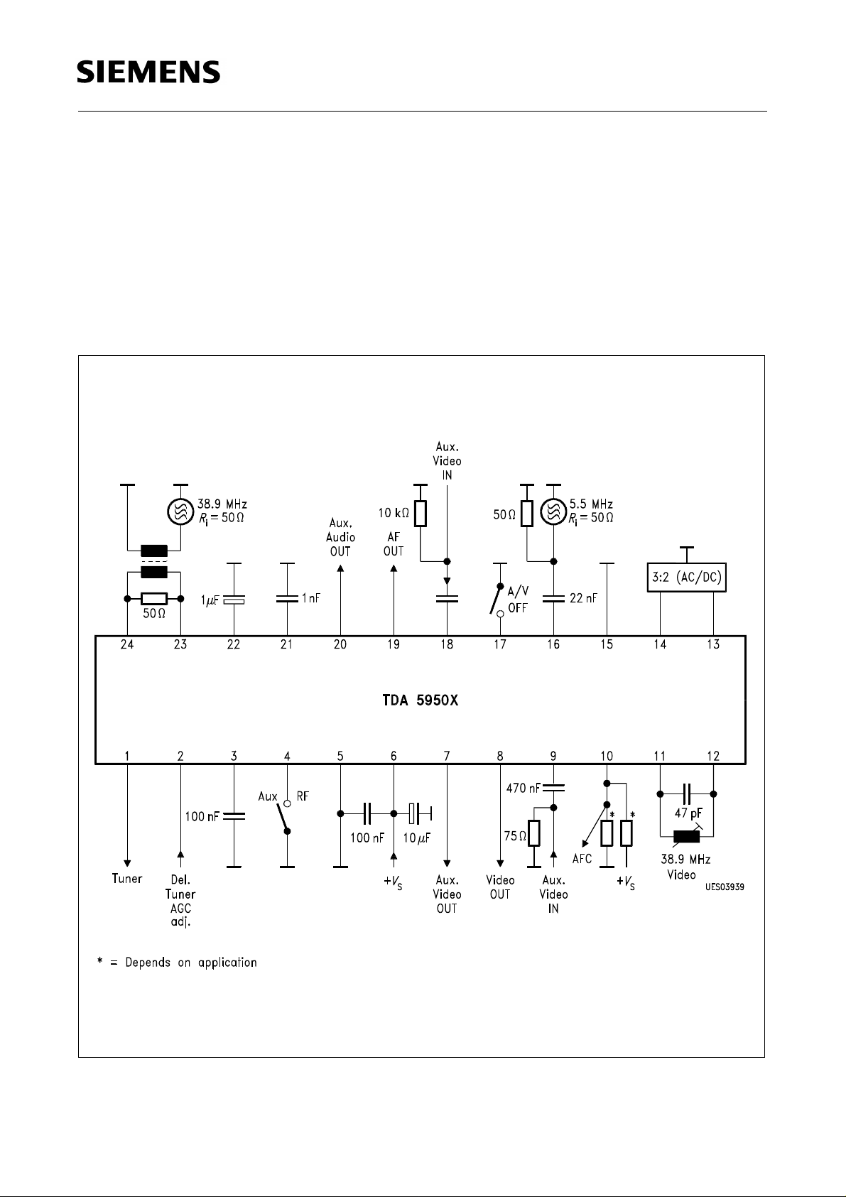
Alignment Instructions
TDA 5950X
At a video carrier input level of V
= 4 mVrms, f
23/24
= 38.9 MHz, and a superimposed AGC
P/C
voltage of V3 = 1.5 V, the demodulator tank circuit is preliminarily aligned until a max. video signal
14 Vpp is obtained at the video output. Any suitable video test signal can be used for modulation.
The AGC voltage V3 is reduced until the signal is approx. 1 Vpp and the max. video signal is
obtained when fine-aligning the demodulator tank circuit. The alignment is not critical due to
relatively large bandwidth of the demodulator tank circuit. Fine-tuning to intercarrier S/N, differential
phase or 2T-pulse characteristics is possible.
Test Circuit
Semiconductor Group 9
Page 10
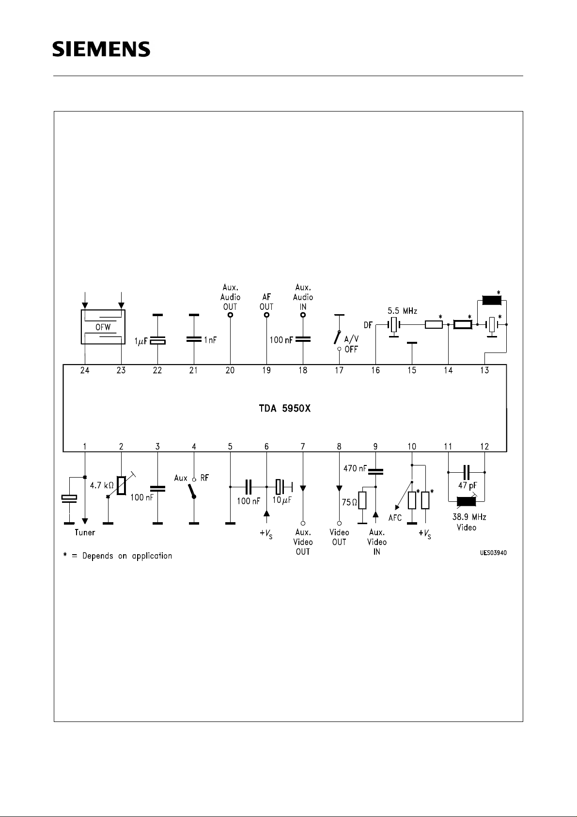
TDA 5950X
Application Circuit
Semiconductor Group 10
Page 11
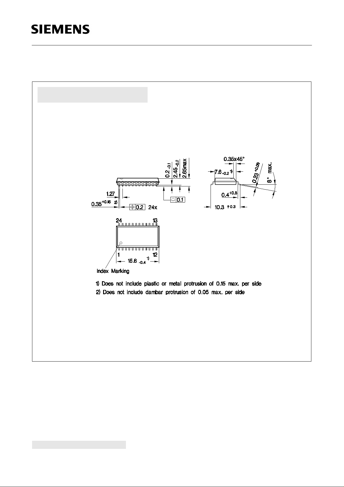
Package Outlines
Plastic-Package, P-DSO-24-1 (SMD)
(Plastic Dual Small Outline)
TDA 5950X
Sorts of Packing
Package outlines for tubes, trays etc. are contained in our
Data Book “Package Information”
SMD = Surface Mounted Device
Semiconductor Group 11
GPS05144
Dimensions in mm
 Loading...