Infineon BCR320U Schematic [ru]

LED Driver
Features
BCR320U / BCR321U
• Continuous output current up to 250mA
with external resistor
• Supply voltage up to 24V
• Digital PWM input up to 10kHz frequency (BCR321U)
• Up to 1W power dissipation in a small SC74 package
• Negative thermal coefficient reduces output current
at higher temperatures
• Easy paralleling of drivers to increase current
• PB-free (RoHS compliant) package
• Automotive qualified according to AEC Q101
Applications
• Architectural LED lighting
• Channel letters for advertising, LED strips for decorative lighting
• Retail lighting in fridge, freezer case and vending machines
• Emergency lighting (e.g. steps lighting, exit way signs etc.)
4
5
6
3
2
1
General Description
The BCR320U/BCR321U provide a low-cost solution for driving 0.5W LEDs with a typical
LED current ILED of 150mA to 200mA. Internal breakdown voltage is >16V, this is the
maximum voltage that the LED driver IC can sustain when the ouput is directly connected
to supply voltage. The BCR320U/BCR321U can be operated at supply voltages of 16V or
higher, by regarding the voltage drop of the LED load, which reduces the supply voltage
to the maximum output voltage of the driver.
The enable pin (BCR320) can withstand a maximum voltage of 25 V, which can also be
increased by stacking a series in front of the LED drivers, resulting in a certain voltage
drop of the LEDs, reducing the voltage at the enable pin below 25V.
A digital input pin (BCR321U) allows dimming via a Microcontroller
with frequencies of up to 10 kHz.
A reduction of the output current at higher temperatures is the result of the negative
temperature coefficient of 0.2 %/K. of the LED drivers.
With no need for additional external components like inductors, capacitors and
free wheeling diodes, the BCR320U/BCR321U LED drivers are a cost-efficient and
PCB-area saving solution for driving 0.5W LEDs.
1
2010-01-15

6 5 4
1 2 3
BCR320U / BCR321U
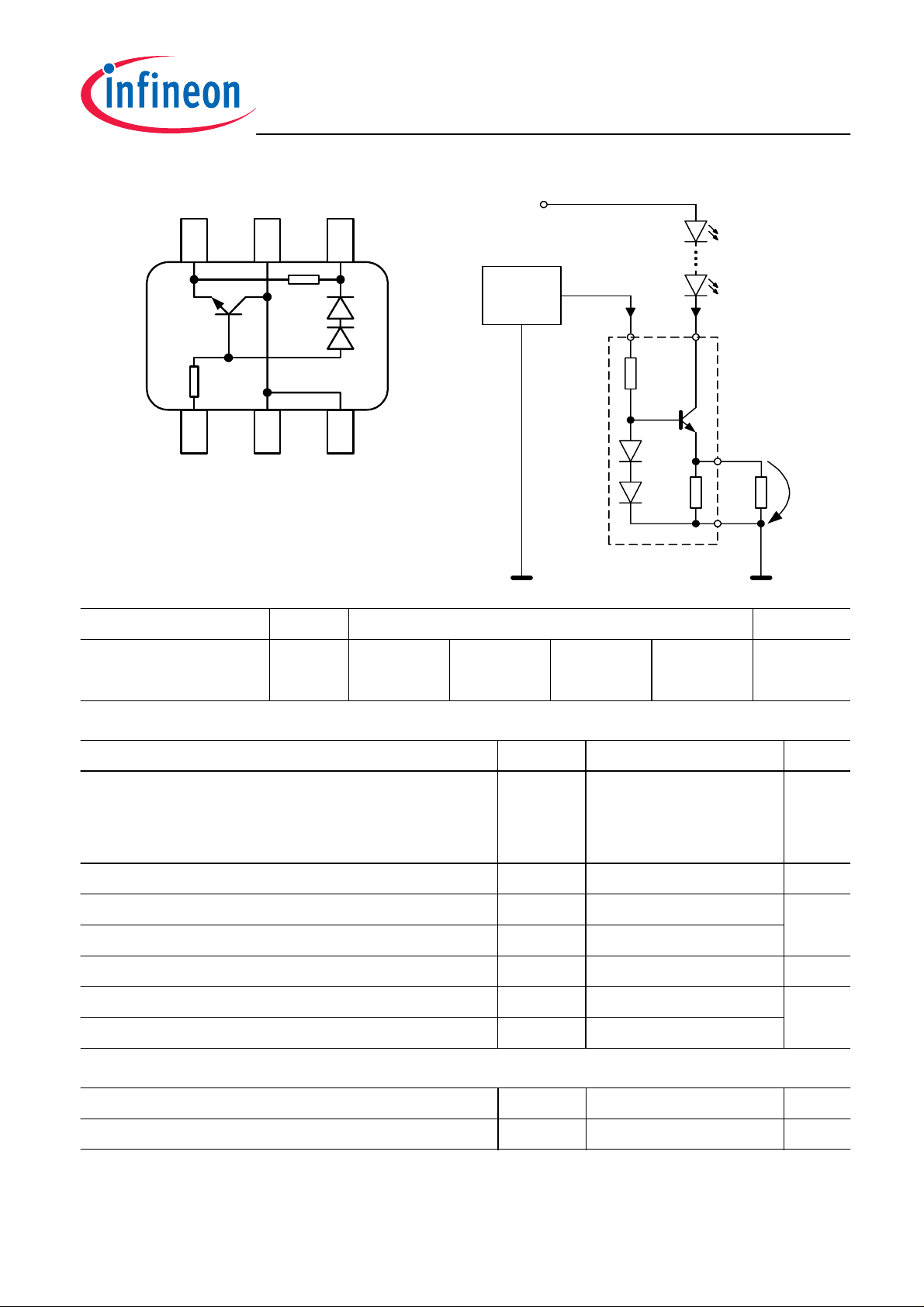
Typical ApplicationPin Configuration
+Vs
µC
I
EN IOUT
1
EN
OUT
2,3,5
Rext
6
Vdrop
GND
4
BCR321U
Type Marking Pin Configuration Package
BCR320U
BCR321U
30
31
1 = EN 2;3;5 =
OUT
4 = GND 6 = R
ext
SC74
SC74
Maximum Ratings
Parameter
Enable voltage
BCR320U
BCR321U
Output current
Output voltage
Reverse voltage between all terminals
Total power dissipation,
T
= 102 °C
S
Junction temperature
Symbol Value Unit
V
EN
V
25
4.5
I
V
V
P
T
out
out
R
tot
j
300 mA
16 V
0.5
1000 mW
150 °C
Storage temperature
Thermal Resistance
Parameter
Junction - soldering point
1
For calculation of
R
please refer to Application Note Thermal Resistance
thJA
1)
T
stg
-65 ... 150
Symbol Value Unit
R
thJS
2
50 K/W
2010-01-15

BCR320U / BCR321U
Electrical Characteristics at
T
=25°C, unless otherwise specified
A
Parameter
Characteristics
Collector-emitter breakdown voltage
I
= 1 mA,
C
I
B
= 0
Enable current
V
= 12 , BCR320U
EN
V
= 3.3 , BCR321U
EN
DC current gain
I
= 50 mA,
C
V
CE
= 1 V
Internal resistor
I
= 10 mA
Rint
Bias resistor
BCR320U
Symbol Values Unit
min. typ. max.
V
BR(CEO)
I
EN
h
FE
R
int
R
B
16 - - V
-
-
1.2
1.2
-
-
200 350 500 -
65 90 105 Ω
-
10
-
mA
kΩ
BCR321U
Output current
V
V
V
out
out
out
= 1.4 V,
= 1.4 V,
= 1.4 V,
V
= 12 V, BCR320U
EN
V
= 3.3 V, BCR321U
EN
V
= 12 V,
EN
R
EXT
= 3 Ω,
BCR320U
V
= 1.4 V,
out
V
EN
= 3.3 ,
R
EXT
= 3 Ω,
BCR321U
Voltage drop (
I
= 10 mA
C
V
Rext
)
DC Characteristics with stabilized LED load
Lowest sufficient supply voltage overhead
I
> 18mA
out
Output current change versus
V
= 12 V;
EN
V
> 2.0 V, BCR320U
out
T
A
I
out
V
drop
V
Smin
∆
I
out/Iout
-
8
8
-
-
1.5
10
10
250
250
-
12
12
-
-
mA
0.85 0.95 1.05 V
- 1.4 - V
-
-0.2
%/K
-
V
= 3.3 V;
EN
V
> 2.0 V, BCR321U
out
Output current change versus
V
V
EN
EN
= 12 V;
= 3.3 V;
V
> 2.0 V, BCR320U
out
V
> 2.0 V, BCR321U
out
V
-
S
∆
I
out/Iout
-
-
3
-0.2
1
1
%/V
-
-
2010-01-15

BCR320U / BCR321U
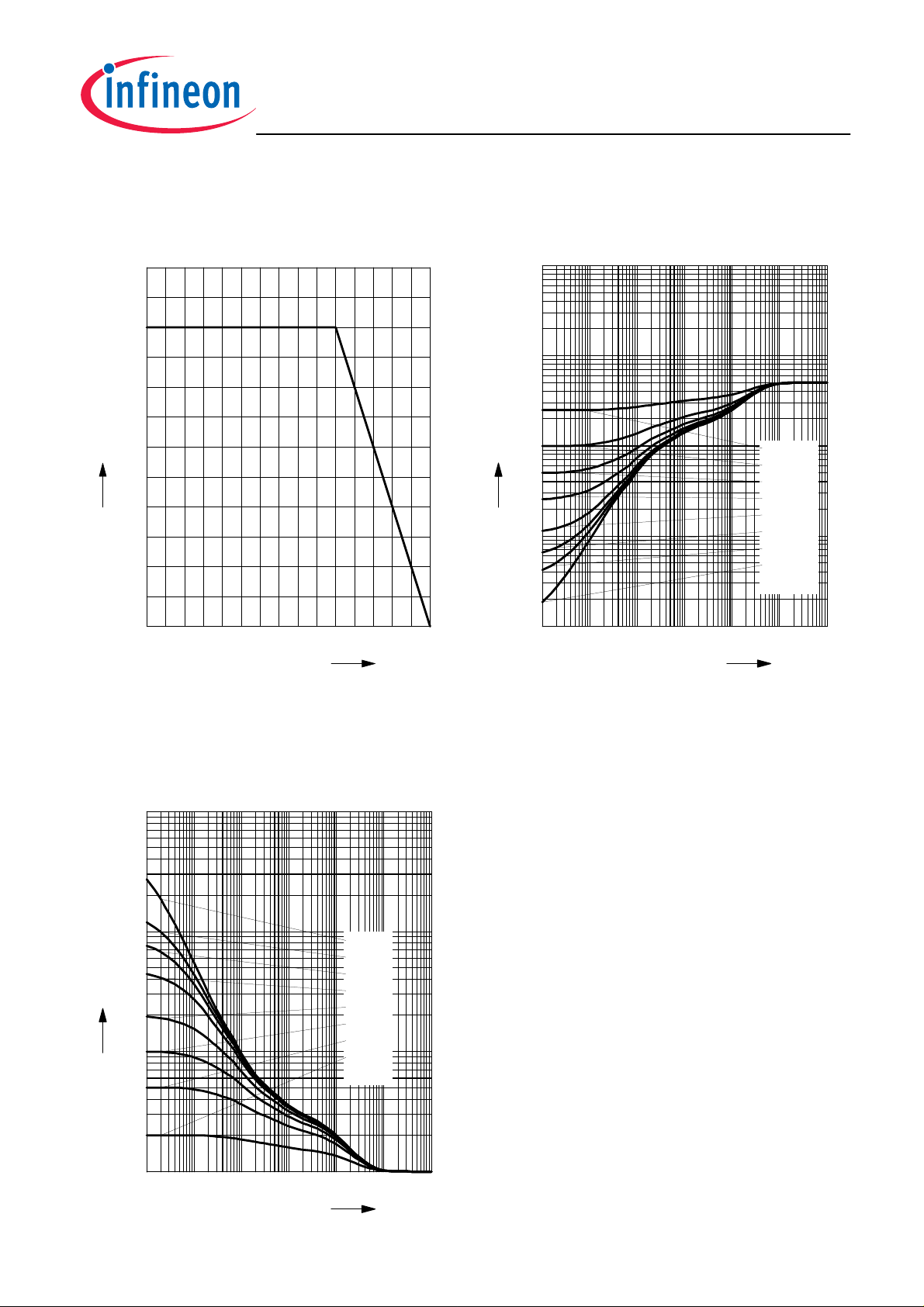
Total power dissipation
1200
mW
1000
900
800
tot
P
700
600
500
400
300
200
100
0
0 20 40 60 80 100 120
P
tot
= f (
T
)
S
Permissible Pulse Load
R
thJS
= f (
t
)
p
3
10
2
10
thJS
R
1
°C
T
10
0
10
-1
10
150
S
10
-6
10
-5
10
-4
10
-3
10
-2
D = 0,5
0,2
0,1
0,05
0,02
0,01
0,005
0
s
T
0
10
P
Permissible Pulse Load
P
totmax
/
P
totDC
= f (
t
)
p
3
10
-
totDC
P
/
2
10
totmax
P
1
10
0
10
10
-6
10
-5
10
-4
10
D = 0
0.005
0.01
0.02
0.05
0.1
0.2
0.5
-3
10
-2
s
T
0
10
P
4
2010-01-15
 Loading...