


 Loading...
945GSE 5.25” SBC
NOVA-945GSE 5.25” SBC
IEI Technology Corp.
MODEL:
NOVA-945GSE
5.25” SBC with 1.6 GHz Intel® Atom™ N270 Processor LVDS/VGA/HDTV, Dual PCIe Mini, Dual PCIe GbE, USB 2.0, SATA and RoHS Compliance
User Manual
Rev. 2.01 – 21 December, 2010
NOVA-945GSE 5.25” SBC
|
|
|
|
Revision |
|
|
|
|
|
|
|
|
|
|
|
|
|
|
Date |
Version |
Changes |
|
|
|
|
|
|
|
|
|
21 |
December, 2010 |
2.01 |
Modified Table 4 6: LVDS1 Panel Resolution Jumper Settings |
|
|
|
|
|
|
|
|
19 |
June, 2009 |
2.00 |
Modified based on the NOVA-945GSE-R20 |
|
|
|
|
|
|
|
|
12 |
March, 2009 |
1.01 |
Changed model name |
|
|
|
|
|
|
|
|
7 November, 2008 |
1.00 |
Initial release |
|
|
|
|
|
|
|
|
Page 1
NOVA-945GSE 5.25” SBC
Copyright
COPYRIGHT NOTICE
The information in this document is subject to change without prior notice in order to improve reliability, design and function and does not represent a commitment on the part of the manufacturer.
In no event will the manufacturer be liable for direct, indirect, special, incidental, or consequential damages arising out of the use or inability to use the product or documentation, even if advised of the possibility of such damages.
This document contains proprietary information protected by copyright. All rights are reserved. No part of this manual may be reproduced by any mechanical, electronic, or other means in any form without prior written permission of the manufacturer.
TRADEMARKS
All registered trademarks and product names mentioned herein are used for identification purposes only and may be trademarks and/or registered trademarks of their respective owners.
Page 2
NOVA-945GSE 5.25” SBC
|
Table of Contents |
|
1 |
INTRODUCTION................................................................................................... |
13 |
|
1.1 INTRODUCTION......................................................................................................... |
14 |
|
1.2 FEATURES................................................................................................................. |
14 |
|
1.3 CONNECTORS ........................................................................................................... |
15 |
|
1.4 DIMENSIONS............................................................................................................. |
16 |
|
1.4.1 External Interface Panel Dimensions .............................................................. |
17 |
|
1.5 DATA FLOW .............................................................................................................. |
18 |
|
1.6 TECHNICAL SPECIFICATIONS .................................................................................... |
19 |
2 |
UNPACKING .......................................................................................................... |
22 |
|
2.1 ANTI-STATIC PRECAUTIONS ...................................................................................... |
23 |
|
2.2 UNPACKING.............................................................................................................. |
23 |
|
2.2.1 Unpacking Precautions.................................................................................... |
23 |
|
2.3 UNPACKING CHECKLIST ........................................................................................... |
24 |
|
2.3.1 Package Contents............................................................................................. |
24 |
|
2.3.2 Optional Items.................................................................................................. |
25 |
3 |
CONNECTORS ...................................................................................................... |
27 |
|
3.1 PERIPHERAL INTERFACE CONNECTORS..................................................................... |
28 |
|
3.1.1 NOVA-945GSE Layout..................................................................................... |
28 |
|
3.2 PERIPHERAL INTERFACE CONNECTORS..................................................................... |
29 |
|
3.2.1 External Interface Panel Connectors............................................................... |
31 |
|
3.3 INTERNAL PERIPHERAL CONNECTORS ...................................................................... |
31 |
|
3.3.1 AT Power Connector........................................................................................ |
31 |
|
3.3.2 ATX Power Supply Enable Connector ............................................................. |
32 |
|
3.3.3 Audio Connector (9-pin) .................................................................................. |
33 |
|
3.3.4 Backlight Inverter Connector .......................................................................... |
34 |
|
3.3.5 Backlight Inverter Connector (for 2nd LVDS Connector) ................................ |
35 |
|
3.3.6 CompactFlash® Socket.................................................................................... |
36 |
|
3.3.7 CRT Connector ................................................................................................ |
38 |
|
3.3.8 Digital Input/Output (DIO) Connector............................................................ |
39 |
Page 3
NOVA-945GSE 5.25” SBC |
|
3.3.9 Fan Connector (+12V, 3-pin) .......................................................................... |
40 |
3.3.10 Front Panel Connector (8-pin) ...................................................................... |
41 |
3.3.11 IDE Connector (44-pin) ................................................................................. |
42 |
3.3.12 Infrared Interface Connector (5-pin)............................................................. |
44 |
3.3.13 Keyboard/Mouse Connector .......................................................................... |
45 |
3.3.14 LVDS LCD Connector (18-bit) ...................................................................... |
46 |
3.3.15 LVDS LCD Connector (18/24-bit) (NOVA-945GSELVDS2 Only) ................ |
47 |
3.3.16 Parallel Port Connector ................................................................................ |
48 |
3.3.17 SATA Drive Connectors ................................................................................. |
50 |
3.3.18 SATA Power Connectors ................................................................................ |
51 |
3.3.19 Serial Port Connectors (COM 1 ~ COM 4)................................................... |
51 |
3.3.20 COM 3 RS-422/485 Connector...................................................................... |
52 |
3.3.21 Trusted Platform Module (TPM) Connector.................................................. |
53 |
3.3.22 TV Out Connector .......................................................................................... |
55 |
3.3.23 USB Connectors (Internal) ............................................................................ |
56 |
3.4 EXTERNAL PERIPHERAL INTERFACE CONNECTOR PANEL ......................................... |
57 |
3.4.1 LAN Connectors............................................................................................... |
57 |
4 INSTALLATION .................................................................................................... |
59 |
4.1 ANTI-STATIC PRECAUTIONS ...................................................................................... |
60 |
4.2 INSTALLATION CONSIDERATIONS.............................................................................. |
61 |
4.2.1 Installation Notices .......................................................................................... |
61 |
4.2.2 Installation Checklist ....................................................................................... |
62 |
4.3 UNPACKING.............................................................................................................. |
63 |
4.4 SO-DIMM AND CF CARD INSTALLATION ................................................................ |
63 |
4.4.1 SO-DIMM Installation ..................................................................................... |
63 |
4.4.2 CF Card Installation........................................................................................ |
64 |
4.5 JUMPER SETTINGS .................................................................................................... |
65 |
4.5.1 AT Power Select Jumper Settings..................................................................... |
66 |
4.5.2 CF Card Setup ................................................................................................. |
67 |
4.5.3 Clear CMOS Jumper........................................................................................ |
68 |
4.5.4 COM 3 Function Select Jumper....................................................................... |
69 |
4.5.5 LVDS Panel Resolution Jumpers ..................................................................... |
70 |
4.5.6 LVDS Voltage Selection Jumpers ..................................................................... |
72 |
4.6 CHASSIS INSTALLATION............................................................................................ |
73 |
Page 4

NOVA-945GSE 5.25” SBC |
|
4.6.1 Airflow.............................................................................................................. |
73 |
4.6.2 Motherboard Installation................................................................................. |
74 |
4.7 INTERNAL PERIPHERAL DEVICE CONNECTIONS........................................................ |
74 |
4.7.1 Audio Kit Installation....................................................................................... |
74 |
4.7.2 Keyboard/Mouse Y-cable Connector ............................................................... |
75 |
4.7.3 Single RS-232 Cable (w/o Bracket) ................................................................. |
77 |
4.7.4 SATA Drive Connection ................................................................................... |
78 |
4.7.5 USB Cable (Dual Port without Bracket) ......................................................... |
79 |
4.8 EXTERNAL PERIPHERAL INTERFACE CONNECTION ................................................... |
80 |
4.8.1 LAN Connection (Single Connector) ............................................................... |
81 |
5 AMI BIOS................................................................................................................ |
82 |
5.1 INTRODUCTION......................................................................................................... |
83 |
5.1.1 Starting Setup................................................................................................... |
83 |
5.1.2 Using Setup ...................................................................................................... |
83 |
5.1.3 Getting Help..................................................................................................... |
84 |
5.1.4 Unable to Reboot After Configuration Changes.............................................. |
84 |
5.1.5 BIOS Menu Bar................................................................................................ |
84 |
5.2 MAIN........................................................................................................................ |
85 |
5.3 ADVANCED ............................................................................................................... |
86 |
5.3.1 CPU Configuration.......................................................................................... |
87 |
5.3.2 IDE Configuration ........................................................................................... |
88 |
5.3.2.1 IDE Master, IDE Slave ............................................................................. |
90 |
5.3.3 Super IO Configuration ................................................................................... |
95 |
5.3.4 Hardware Health Configuration.................................................................... |
100 |
5.3.5 Power Configuration...................................................................................... |
103 |
5.3.6 APM Configuration........................................................................................ |
105 |
5.3.7 Remote Configuration .................................................................................... |
107 |
5.3.8 USB Configuration.......................................................................................... |
111 |
5.3.9 Trusted Computing .......................................................................................... |
113 |
5.4 PCI/PNP.................................................................................................................. |
114 |
5.5 BOOT....................................................................................................................... |
116 |
5.5.1 Boot Settings Configuration............................................................................ |
116 |
5.6 SECURITY................................................................................................................ |
119 |
5.7 CHIPSET ................................................................................................................. |
120 |
Page 5

|
|
NOVA-945GSE 5.25” SBC |
|
5.7.1 North Bridge Chipset Configuration ............................................................. |
121 |
|
5.7.1.1 Video Function Configuration ................................................................ |
122 |
|
5.7.2 SouthBridge Configuration............................................................................ |
125 |
|
5.8 EXIT ....................................................................................................................... |
126 |
6 |
SOFTWARE DRIVERS ....................................................................................... |
128 |
|
6.1 AVAILABLE SOFTWARE DRIVERS ............................................................................ |
129 |
|
6.2 STARTING THE DRIVER PROGRAM .......................................................................... |
129 |
|
6.3 CHIPSET DRIVER INSTALLATION............................................................................. |
131 |
|
6.4 VGA DRIVER INSTALLATION.................................................................................. |
136 |
|
6.5 LAN DRIVER INSTALLATION.................................................................................. |
141 |
|
6.6 AUDIO DRIVER INSTALLATION ............................................................................... |
143 |
A |
BIOS MENU OPTIONS....................................................................................... |
147 |
B |
TERMINOLOGY ................................................................................................. |
151 |
C |
DIO INTERFACE................................................................................................. |
156 |
|
C.1 DIO INTERFACE INTRODUCTION............................................................................ |
157 |
|
C.2 DIO CONNECTOR PINOUTS.................................................................................... |
157 |
|
C.3 ASSEMBLY LANGUAGE SAMPLES........................................................................... |
158 |
|
C.3.1 Enable the DIO Input Function..................................................................... |
158 |
|
C.3.2 Enable the DIO Output Function .................................................................. |
158 |
D |
WATCHDOG TIMER .......................................................................................... |
159 |
E |
ADDRESS MAPPING.......................................................................................... |
162 |
|
E.1 I/O ADDRESS MAP ................................................................................................. |
163 |
|
E.2 IRQ ADDRESS MAP ............................................................................................... |
165 |
|
E.3 MEMORY ADDRESS MAP........................................................................................ |
166 |
F |
HAZARDOUS MATERIALS DISCLOSURE................................................... |
167 |
|
F.1 HAZARDOUS MATERIAL DISCLOSURE TABLE FOR IPB PRODUCTS CERTIFIED AS ROHS |
|
|
COMPLIANT UNDER 2002/95/EC WITHOUT MERCURY ................................................ |
168 |
Page 6

NOVA-945GSE 5.25” SBC
List of Figures |
|
Figure 1-1: NOVA-945GSE.......................................................................................... |
14 |
Figure 1-2: NOVA-945GSE Overview [Front View]................................................... |
15 |
Figure 1-3: NOVA-945GSE Overview [Solder Side] ................................................. |
16 |
Figure 1-4: NOVA-945GSE Dimensions (mm) .......................................................... |
17 |
Figure 1-5: External Interface Panel Dimensions (mm)........................................... |
17 |
Figure 1-6: Data Flow Block Diagram........................................................................ |
18 |
Figure 3-1: Connector and Jumper Locations [Front Side].................................... |
28 |
Figure 3-2: Connector and Jumper Locations [Solder Side].................................. |
29 |
Figure 3-3: AT Power Connector Location ............................................................... |
32 |
Figure 3-4: ATX Power Supply Enable Connector Location................................... |
33 |
Figure 3-5: Audio Connector Location (9-pin) ......................................................... |
34 |
Figure 3-6: Panel Backlight Connector Pinout Locations....................................... |
35 |
Figure 3-7: Panel Backlight Connector (2) Pinout Locations ................................. |
36 |
Figure 3-8: CF Card Socket Location........................................................................ |
37 |
Figure 3-9: VGA Connector Pinout Locations.......................................................... |
39 |
Figure 3-10: DIO Connector Connector Locations .................................................. |
40 |
Figure 3-11: +12V Fan Connector Location.............................................................. |
41 |
Figure 3-12: Front Panel Connector Pinout Locations (8-pin) ............................... |
42 |
Figure 3-13: Secondary IDE Device Connector Locations...................................... |
43 |
Figure 3-14: Infrared Connector Pinout Locations .................................................. |
44 |
Figure 3-15: Keyboard/Mouse Connector Location................................................. |
45 |
Figure 3-16: LVDS LCD Connector Pinout Location ............................................... |
46 |
Figure 3-17: LVDS LCD Connector Pinout Location ............................................... |
47 |
Figure 3-18: Parallel Port Connector Location......................................................... |
49 |
Figure 3-19: SATA Drive Connector Locations........................................................ |
50 |
Figure 3-20: SATA Power Connector Locations ...................................................... |
51 |
Figure 3-21: COM Connector Pinout Locations ....................................................... |
52 |
Figure 3-22: COM 3 RS-422/485 Connector Pinout Locations................................ |
53 |
Page 7

NOVA-945GSE 5.25” SBC
Figure 3-23: TPM Connector Pinout Locations........................................................ |
54 |
Figure 3-24: TV Connector Pinout Locations........................................................... |
55 |
Figure 3-25: USB Connector Pinout Locations........................................................ |
56 |
Figure 3-26: NOVA-945GSE External Peripheral Interface Connector .................. |
57 |
Figure 3-27: RJ-45 Ethernet Connector .................................................................... |
58 |
Figure 4-1: SO-DIMM Installation............................................................................... |
63 |
Figure 4-2: CF Card Installation................................................................................. |
65 |
Figure 4-3: Jumper Locations.................................................................................... |
65 |
Figure 4-4: AT Power Select Jumper Location ........................................................ |
67 |
Figure 4-5: CF Card Setup Jumper Location............................................................ |
68 |
Figure 4-6: Clear CMOS Jumper................................................................................ |
69 |
Figure 4-7: COM 3 Function Select Jumper Location ............................................. |
70 |
Figure 4-8: LVDS Panel Resolution Jumper Pinout Locations .............................. |
71 |
Figure 4-9: LVDS Voltage Selection Jumper Pinout Locations.............................. |
73 |
Figure 4-10: Audio Kit Cable Connection ................................................................. |
75 |
Figure 4-11: Keyboard/mouse Y-cable Connection................................................. |
76 |
Figure 4-12: Single RS-232 Cable Installation.......................................................... |
77 |
Figure 4-13: SATA Drive Cable Connection ............................................................. |
78 |
Figure 4-14: SATA Power Drive Connection ............................................................ |
79 |
Figure 4-15: Dual USB Cable Connection................................................................. |
80 |
Figure 4-16: LAN Connection..................................................................................... |
81 |
Figure 6-1: Start Up Screen..................................................................................... |
130 |
Figure 6-2: Select Operating System ..................................................................... |
130 |
Figure 6-3: Drivers.................................................................................................... |
131 |
Figure 6-4: Chipset Driver Screen .......................................................................... |
132 |
Figure 6-5: Chipset Driver Welcome Screen ......................................................... |
132 |
Figure 6-6: Chipset Driver License Agreement..................................................... |
133 |
Figure 6-7: Chipset Driver Read Me File ................................................................ |
134 |
Figure 6-8: Chipset Driver Setup Operations ........................................................ |
135 |
Figure 6-9: Chipset Driver Installation Finish Screen .......................................... |
136 |
Figure 6-10: VGA Driver Read Me File.................................................................... |
137 |
Figure 6-11: VGA Driver Setup Files Extracted..................................................... |
137 |
Page 8
NOVA-945GSE 5.25” SBC
Figure 6-12: VGA Driver Welcome Screen............................................................. |
138 |
Figure 6-13: VGA Driver License Agreement ........................................................ |
139 |
Figure 6-14: VGA Driver Read Me File.................................................................... |
139 |
Figure 6-15: VGA Driver Setup Operations ........................................................... |
140 |
Figure 6-16: VGA Driver Installation Finish Screen.............................................. |
140 |
Figure 6-17: LAN Driver Welcome Screen ............................................................. |
141 |
Figure 6-18: LAN Driver Welcome Screen ............................................................. |
142 |
Figure 6-19: LAN Driver Installation....................................................................... |
142 |
Figure 6-20: LAN Driver Installation Complete ..................................................... |
143 |
Figure 6-21: Audio Driver Options.......................................................................... |
144 |
Figure 6-22: AC’97 Driver Installation Welcome Screen ...................................... |
145 |
Figure 6-23: AC’97 Driver Installation Verification............................................. |
145 |
Figure 6-24: AC’97 Driver Installation .................................................................... |
146 |
Figure 6-25: AC’97 Driver Installation Complete................................................... |
146 |
Page 9

NOVA-945GSE 5.25” SBC
List of Tables |
|
Table 1-1: Technical Specifications .......................................................................... |
21 |
Table 3-1: Peripheral Interface Connectors.............................................................. |
31 |
Table 3-2: Rear Panel Connectors............................................................................. |
31 |
Table 3-3: AT Power Connector Pinouts .................................................................. |
32 |
Table 3-4: ATX Power Supply Enable Connector Pinouts ...................................... |
33 |
Table 3-5: Audio Connector Pinouts (9-pin)............................................................. |
34 |
Table 3-6: Panel Backlight Connector Pinouts ........................................................ |
35 |
Table 3-7: Panel Backlight Connector (2) Pinouts................................................... |
36 |
Table 3-8: CF Card Socket Pinouts ........................................................................... |
38 |
Table 3-9: VGA Connector Pinouts ........................................................................... |
39 |
Table 3-10: DIO Connector Pinouts........................................................................... |
40 |
Table 3-11: +12V Fan Connector Pinouts ................................................................. |
41 |
Table 3-12: Front Panel Connector Pinouts (8-pin) ................................................. |
42 |
Table 3-13: Secondary IDE Connector Pinouts........................................................ |
44 |
Table 3-14: Infrared Connector Pinouts.................................................................... |
44 |
Table 3-15: Keyboard/Mouse Connector Pinouts .................................................... |
45 |
Table 3-16: LVDS LCD Port Connector Pinouts....................................................... |
47 |
Table 3-17: LVDS LCD Port Connector Pinouts....................................................... |
48 |
Table 3-18: Parallel Port Connector Pinouts ............................................................ |
49 |
Table 3-19: SATA Drive Connector Pinouts ............................................................. |
50 |
Table 3-20: SATA Power Connector Pinouts ........................................................... |
51 |
Table 3-21: COM Connector Pinouts......................................................................... |
52 |
Table 3-22: COM 3 RS-422/485 Connector Pinouts ................................................. |
53 |
Table 3-23: TPM Connector Pinouts.......................................................................... |
54 |
Table 3-24: TV Port Connector Pinouts .................................................................... |
55 |
Table 3-25: USB Port Connector Pinouts ................................................................. |
56 |
Table 3-26: LAN Pinouts............................................................................................. |
57 |
Table 3-27: RJ-45 Ethernet Connector LEDs............................................................ |
58 |
Page 10

NOVA-945GSE 5.25” SBC
Table 4-1: Jumpers...................................................................................................... |
66 |
Table 4-2: AT Power Select Jumper Settings........................................................... |
66 |
Table 4-3: CF Card Setup Jumper Settings .............................................................. |
67 |
Table 4-4: Clear CMOS Jumper Settings .................................................................. |
69 |
Table 4-5: COM 3 Function Select Jumper Settings................................................ |
70 |
Table 4-6: LVDS1 Panel Resolution Jumper Settings ............................................. |
71 |
Table 4-7: LVDS2 Panel Resolution Jumper Settings ............................................. |
71 |
Table 4-8: LVDS Voltage Selection Jumper Settings .............................................. |
72 |
Table 5-1: BIOS Navigation Keys............................................................................... |
84 |
Page 11
NOVA-945GSE 5.25” SBC
List of BIOS Menus |
|
Menu 1: Main................................................................................................................ |
85 |
Menu 2: Advanced....................................................................................................... |
87 |
Menu 3: CPU Configuration ....................................................................................... |
87 |
Menu 4: IDE Configuration ......................................................................................... |
88 |
Menu 5: IDE Master and IDE Slave Configuration ................................................... |
90 |
Menu 6: Super IO Configuration................................................................................ |
95 |
Menu 7: Hardware Health Configuration ............................................................... |
100 |
Menu 8: Power Configuration ................................................................................. |
104 |
Menu 9:Advanced Power Management Configuration......................................... |
105 |
Menu 10: Remote Access Configuration [Advanced] .......................................... |
108 |
Menu 11: USB Configuration .................................................................................. |
111 |
Menu 12: Trusted Computing.................................................................................. |
113 |
Menu 13: PCI/PnP Configuration............................................................................ |
114 |
Menu 14: Boot........................................................................................................... |
116 |
Menu 15: Boot Settings Configuration................................................................... |
117 |
Menu 16: Security..................................................................................................... |
119 |
Menu 17: Chipset...................................................................................................... |
120 |
Menu 18:North Bridge Chipset Configuration....................................................... |
121 |
BIOS Menu 39:Northbridge Chipset Configuration .............................................. |
123 |
Menu 19:SouthBridge Chipset Configuration ....................................................... |
125 |
Menu 20:Exit ............................................................................................................. |
126 |
Page 12
NOVA-945GSE 5.25” SBC
Chapter
1
Introduction
Page 13
NOVA-945GSE 5.25” SBC
1.1 Introduction
Figure 1-1: NOVA-945GSE
The NOVA-945GSE 5.25” motherboard is embedded 45 nm Intel® Atom™ processor platforms. The Intel® Atom™ processor N270 embedded on the NOVA-945GSE has a 1.60 GHz clock speed, a 533 MHz FSB and a 512 KB L2 cache. The NOVA-945GSE also supports one 200-pin 533 MHz 2.0 GB (max.) DDR2 SDRAM SO-DIMM. The board comes with a LVDS connector that supports 18-bit dual-channel LVDS screens. The NOVA-945GSELVDS2-N270 model has an additional LVDS connector and supports 18-bit or 24-bit dual-channel LVDS device. The NOVA-945GSE also comes with two PCI Express (PCIe) Gigabit Ethernet (GbE) connectors, two PCIe mini card slots, one PCI slot and one PC/104-Plus expansion slot.
1.2 Features
Some of the NOVA-945GSE motherboard features are listed below:
5.25” form factor
1.6 GHz Intel® Atom™ N270 processor Fanless
DDR2 400/533 MHz SO-DIMM memory support up to 2.0 GB Supports dual PCIe mini cards
Supports one PCI expansion slot
Page 14
NOVA-945GSE 5.25” SBC
Dual LVDS support dual display output
TPM support
1.3 Connectors
The NOVA-945GSE has a wide variety of peripheral interface connectors. Figure5 1-2 is a labeled photo of the peripheral interface connectors on the NOVA-945GSE.
Figure 1-2: NOVA-945GSE Overview [Front View]
Figure 1-3 shows the rear side of the NOVA-945GSE.
Page 15

NOVA-945GSE 5.25” SBC
Figure 1-3: NOVA-945GSE Overview [Solder Side]
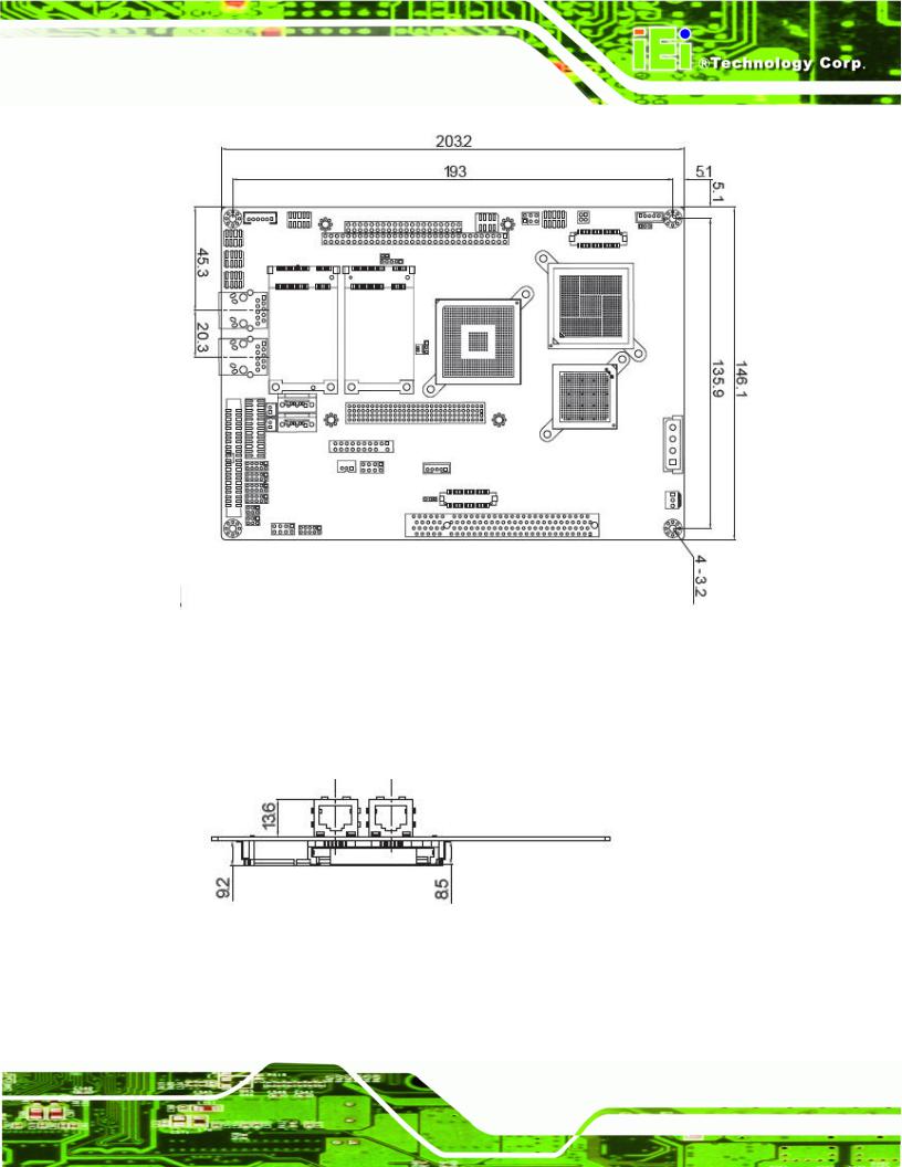
1.4 Dimensions
The dimensions of the board are listed below:
Length: |
203 mm |
Width: |
146 mm |
Page 16
NOVA-945GSE 5.25” SBC
Figure 1-4: NOVA-945GSE Dimensions (mm)
1.4.1 External Interface Panel Dimensions
External peripheral interface connector panel dimensions are shown in Figure5 1-5.
Figure 1-5: External Interface Panel Dimensions (mm)
Page 17

NOVA-945GSE 5.25” SBC
1.5 Data Flow
Figure5 1-6 shows the data flow between the two on-board chipsets and other components installed on the motherboard and described in the following sections of this chapter.
Figure 1-6: Data Flow Block Diagram
Page 18
NOVA-945GSE 5.25” SBC
1.6 Technical Specifications
NOVA-945GSE technical specifications are listed in the table below. See Chapter 2 for details.
Specification |
NOVA-945GSE |
|
|
Form Factor |
5.25” |
|
|
CPU |
45 nm 1.6 GHz Intel® Atom™ N270 |
|
|
Front Side Bus (FSB) |
533 MHz |
|
|
Northbridge Chipset |
Intel® 945GSE |
|
|
Southbridge Chipset |
Intel® ICH7-M |
|
|
Memory |
One 200-pin SO-DIMM socket supports one 533/400 MHz |
|
2.0 GB (max.) DDR2 SDRAM SO-DIMM |
|
|
SSD |
One CompactFlash® Type II socket |
|
|
Audio |
Realtek ALC655 AC'97 codec |
|
|
LAN |
Two Realtek RTL8111CP GbE controllers |
|
|
Super I/O Controller |
ITE IT8718F |
|
|
Serial Port Controller |
Fintek F81216 |
|
|
BIOS |
AMI BIOS label |
|
|
Watchdog Timer |
Software programmable supports 1~255 sec. system reset |
|
|
Expansion |
|
|
|
PCI |
One PCI slot |
|
|
PCIe |
Two PCIe mini card slots |
|
|
PC/104 |
One PC/104-Plus slot (ISA + PCI bus) |
|
|
I/O Interface Connectors |
|
|
|
Audio Connector |
One internal audio connector (10-pin header) |
|
|
Page 19

NOVA-945GSE 5.25” SBC
|
Specification |
NOVA-945GSE |
|
|
|
|
|
|
Display port |
|
One VGA |
|
|
|
One TV-out connector support HDTV by component interface |
|
|
|
One 18-bit dual channel LVDS connector |
|
|
|
One 18/24-bit dual channel LVDS connector |
|
|
|
(NOVA-945GSELVDS2-N270 only) |
|
|
|
|
|
Ethernet |
Two RJ-45 GbE ports |
|
|
|
|
|
|
Keyboard/Mouse |
One 6-pin header for keyboard and mouse |
|
|
|
|
|
|
Parallel Port |
|
One IEEE 1284 parallel port (26-pin header) supporting |
|
|
|
normal, EPP and ECP modes |
|
|
|
|
|
Serial Ports |
|
Five via internal pin headers |
|
|
|
Three RS-232 |
|
|
|
One RS-232/422/485 |
|
USB 2.0/1.1 ports |
Six USB 2.0 devices supported by on-board pin-headers |
|
|
|
|
|
|
|
|
One infrared connector through the ITE super I/O. Supports: |
|
Infrared |
|
Serial Infrared (SIR) |
|
|
|
Amplitude Shift Keyed IR (ASKIR) |
|
TPM |
One 20-pin header supports TPM function |
|
|
|
|
|
|
Digital I/O |
|
One 8-bit digital input/output connector; 4-bit input/4-bit output |
|
|
through the ITE IT8718F super I/O |
|
|
|
|
|
|
|
|
|
|
Storage |
|
|
|
|
|
|
|
Serial ATA |
|
Two independent serial ATA (SATA) channels with 1.5 Gb/s |
|
|
|
data transfer rates |
|
|
|
|
|
IDE |
|
One 44-pin IDE connector connects to two Ultra |
|
|
|
ATA33/66/100 devices |
|
|
|
|
Page 20

NOVA-945GSE 5.25” SBC
Specification |
NOVA-945GSE |
|
|
Environmental and Power Specifications |
|
|
|
Power Supply |
ATX and AT power supported |
|
|
Power Consumption |
5 V @ 3.49 A |
|
1.6 GHz Intel® Atom™ N270 CPU with one 512 MB DDR2 |
|
SO-DIMM |
|
|
Operating temperature |
0ºC – 60ºC (32ºF - 140ºF) |
|
|
Humidity |
5% ~ 95% (non-condensing) |
|
|
Physical Specifications |
|
|
|
Dimensions |
203 mm x 146 mm |
|
|
Weight GW/NW |
1000g/400g |
|
|
Table 1-1: Technical Specifications
Page 21
NOVA-945GSE 5.25” SBC
Chapter
2
Unpacking
Page 22
NOVA-945GSE 5.25” SBC
2.1 Anti-static Precautions
 WARNING!
Failure to take ESD precautions during the installation of the
NOVA-945GSE may result in permanent damage to the
NOVA-945GSE and severe injury to the user.
Electrostatic discharge (ESD) can cause serious damage to electronic components, including the NOVA-945GSE. Dry climates are especially susceptible to ESD. It is therefore critical that whenever the NOVA-945GSE, or any other electrical component is handled, the following anti-static precautions are strictly adhered to.
Wear an anti-static wristband: - Wearing a simple anti-static wristband can help to prevent ESD from damaging the board.
Self-grounding:- Before handling the board touch any grounded conducting material. During the time the board is handled, frequently touch any conducting materials that are connected to the ground.
Use an anti-static pad: When configuring the NOVA-945GSE, place it on an antic-static pad. This reduces the possibility of ESD damaging the NOVA-945GSE.
Only handle the edges of the PCB:- When handling the PCB, hold the PCB by the edges.
2.2Unpacking
2.2.1Unpacking Precautions
When the NOVA-945GSE is unpacked, please do the following:
Follow the anti-static precautions outlined in Section 25 .1.
Make sure the packing box is facing upwards so the NOVA-945GSE does not fall out of the box.
Make sure all the components shown in Section 25 .3 are present.
Page 23
NOVA-945GSE 5.25” SBC
2.3 Unpacking Checklist
 NOTE:
NOTE:
If any of the components listed in the checklist below are missing, do not proceed with the installation. Contact the IEI reseller or vendor the NOVA-945GSE was purchased from or contact an IEI sales representative directly by sending an email to sales@iei2 .com.tw.
2.3.1 Package Contents
The NOVA-945GSE is shipped with the following components:
Quantity |
Item and Part Number |
Image |
|
|
|
1 |
NOVA-945GSE |
|
|
|
|
1 |
Audio cable |
|
|
(P/N: 32000-072100-RS) |
|
|
|
|
1 |
KB/MS PS/2 Y-cable |
|
|
(P/N: 32000-023800-RS) |
|
|
|
|
4 |
RS-232 cable (w/o bracket) |
|
|
(P/N: 32200-000049-RS) |
|
|
|
|
2 |
SATA cable |
|
|
(P/N: 32000-062800-RS) |
|
|
|
|
1 |
Dual USB cable (w/o bracket) |
|
|
(P/N: 32000-070301-RS) |
|
|
|
|
Page 24
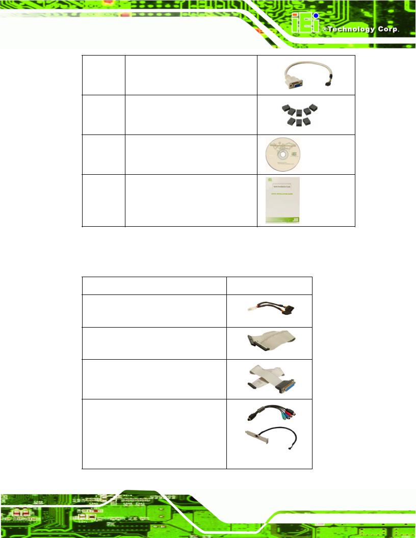
NOVA-945GSE 5.25” SBC
1VGA cable
(P/N: 32000-033804-RS)
1Mini jumper pack (2.0mm) (P/N: 33100-000033-RS)
1 |
Utility CD |
1 |
Quick Installation Guide |
2.3.2 Optional Items
The NOVA-945GSE is shipped with the following components:
Item and Part Number |
Image |
SATA power cable
(P/N: 32100-088600-RS)
HDD cable
(P/N: 32200-000009-RS)
LPT cable (w/o bracket) (P/N: 32200-015100-RS)
HDTV output cable
(P/N: HDTVCABLESET-01)
Page 25
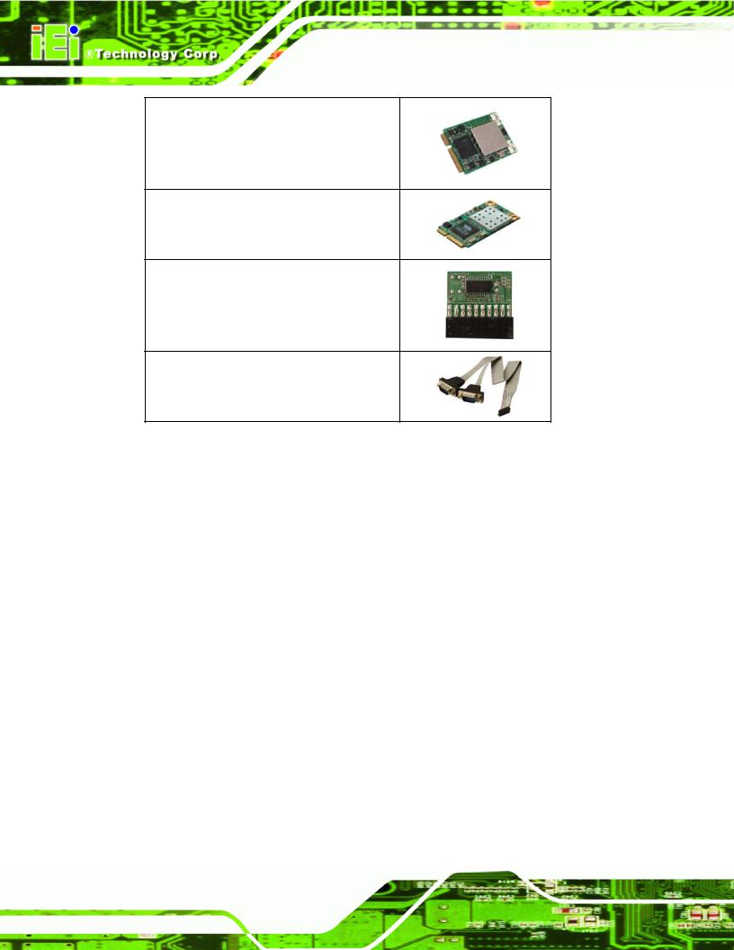
NOVA-945GSE 5.25” SBC
802.11 b/g PCIe mini card wireless LAN module with Atheros
(P/N: WMPCIE-V01-R10)
802.11b/g USB embedded module with VIA (P/N: WMUSB-V01-R10)
20-pin WINBOND TPM module and S/W management Tool
(P/N: TPM-WI01-R10)
RS-422/485 cable
(P/N: 32200-833600-RS)
Page 26
NOVA-945GSE 5.25” SBC
Chapter
3
Connectors
Page 27
NOVA-945GSE 5.25” SBC
3.1 Peripheral Interface Connectors
Section 3.1.1 shows peripheral interface connector locations. Section 3.3 lists all the peripheral interface connectors seen in Section 3.1.1.
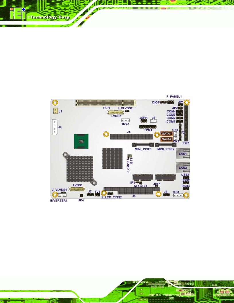
3.1.1 NOVA-945GSE Layout
Figure6 3-1 shows the on-board peripheral connectors, rear panel peripheral connectors
and on-board jumpers.
Figure 3-1: Connector and Jumper Locations [Front Side]
Figure 3-2 shows the solder side of the NOVA-945GSE.
Page 28
Loading...