

Page 1
查询IDT RC5000供应商
MULTI-ISSUE
64-BIT MICROPROCESSOR
In tegrat ed De v i ce Technology, I nc.
FEATURES
• Dual issue super-scalar execution core, executing at
high-frequency
- 250 MHz frequency
- Dual issue floating-point ALU operations with other
instruction classes
- Traditional 5-stage pipeline, minim izes load and
branch latencies
- Single cycle repeat rate for most floating point ALU
operations
• High level of performance for a variety of applications
- High-performance 64-bit integer unit achieves 330
dhrystone MIPS (dhrystone 2.1)
- Ultra high-performance floating-point accelerator,
directly implementin g single- and double-precision
operations achieves 500mflops
- Extremely large on-chip primary caches
- On-chip secondary cache controller
• Large, efficient on-chip caches
- 32KB Instruction Cache, 32KB Data Cache
- 2-set associative in each cache
- Virtually indexed and physically tagged to minimize
cache flushes
- Write-back and write-through selectable on a per
page basis
- Critical word first cache miss processing
- Supports back-to-back loads and stores in any combination at full pipeline rate
IDT RC5000
• High-performance memory system
- Large primary caches integrated on-chip
- Secondary cac he con trol interface on-chip
- High-frequency 64-bit bus interface runs up to
100MHz
- Aggregate bandwidth of on-chip caches, system
interface of 5GB/s
- High-performance write protocols for graphics and
data communications
• MIPS-IV 64-bit ISA for improved computation
- Compound floating-point operations for 3D graphics
and floating-point DSP
- Conditional move operations
• Compatible with a variety of operating systems
- Windows™ CE
- Numerous MIPS-compatible real-time operating systems
• Uses input system clock, with processor pipeline
clock multiplied by a factor of 2-8
• Large on-chip TLB
• Active power management, including use of WAIT
operation
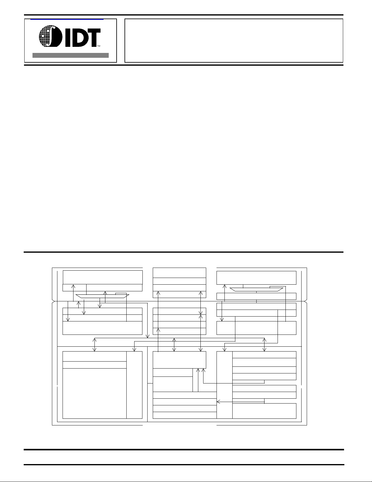
BLOCK DIAGRAM
Control
Floating Point Register File
Unpacker/Packer
Floating Point
MAdd,Add,Sub, Cvt
Div, SqRt
Data Set A
Store Buffer
Write Buffer
Read Buffer
Data Set B
DBus
SysAD
FPIBus
Floating-point Control
Phase Lock Loop
Data Tag A
DTLB Physical
Address Buffer
Instruction Tag A
ITLB Physical
Instruction Tag B
Tag
Coprocessor 0
System/Memory
Instruction TLB Virtual
AuxTag
Joint TLB
Control
PC Incrementer
Branch Adder
Program Counter
IVA
DV A
Instruction Set A
Instruction Select
Integer Instruction Register
FP Instruction Register
Instruction Set B
IntIBus
Load Aligner
Integer Register File
Integer Control
Integer/Address Adder
Data TLB Virtual
Shifter/Store Aligner
Logic Unit
ABus
Integer Multiply, Divide
The IDT logo is a registered trademark and ORION, R4600, R4640, R4650, R4700, R5000, RV5000, and RISController are trademarks of Integrated Device Technology, Inc. MIPS is a registered
trademark of MIPS Computer Systems, Inc.
COMMERCIAL TEMPERATURE RANGE
1998 Integrated Device Technology, Inc. 1
June, 1998
Page 2
IDT RC5000 COMMERCIAL TEMPERATURE RANGE
DESCRIPTION
The RC5000 serves many performance critical
embedded applications, such as high-end internetworking systems, color printers, and graphics terminals.
The RC5000 is optimized for high-performa nce appli cations, with special emphasis on s ystem bandwidth and
floating point operations, through integration of highperformance computa t io nal un its a nd a high-performance
memory hierarchy. For this class of applica tion, the result
is a relatively low-cost CPU capable of approximately 330
Dhrystone MIPS.
IDT’s objectives in offering the RC5000 include:
• Offering a high performance upgrade path to existing
embedded customers in the internetworking, office
automation and visualization markets.
• Providing a significant improvement in the floating-
point performance currently available in a moderately
priced MIPS CPU.
• Providing improvements in the memory hierarchy of
desktop systems by using large primary caches and
integrating a secondary cache controller.
• Enabling improvements in performance through the
use of the MIPS-IV ISA.
Instruction Issue Mechanism
The RC5000 recognizes two general classes of
instructions for multi-issue:
• Floating-point ALU
• All others
These instruction classes are pre-decoded by the
RC5000, as they are brough t on-chip. The pre-de coded
information is stored in the instruction cache.
Assuming that there are no pending resource
conflicts, the RC5000 can issue one instr uction per cl ass
per pipeline clock cycle. Note that this broad separation of
classes insures that there are no data dependencies to
restrict multi-issue.
However, long-latency resources in either the floatingpoint ALU (e.g. DIV or SQRT instru ctions) or instr uctions
in the integer unit (such as multiply) can restrict the issue
of instructions. Note that the R5000 does not perform outof-order or speculative execution; instead, the pipeline
slips until the required resource becomes available.
There are no alignment restrictions on dual-issue
instruction pairs. The RC5000 fetches two instructions
from the cache per cycl e. Thus, for optimal performance,
compilers should atte mpt to align branch target s to allow
dual-issue on the first target cycle, since the instruction
cache only performs aligned fetches.
Integer Pipeline
The RC5000 is a limited dual-issue machine that
utilizes a traditional 5-stage integer pipeline. This basic
integer pipeline of the RC5000 is illustrated in Figure 1.
The integer instruction execution speed is tabulated
(in number of pipeline clocks) as follows:
Operation Latency Repeat
Load 2 1
Store 2 1
MULT/MUL TU 8 8
DMULT/DMULTU 12 12
DIV/DIVU 36 36
DDIV/DDIVU 68 68
Other Integer ALU 1 1
Branch 2 2
Jump 2 2
The RC5000’s short pipeline keeps the load and
branch latencies very low. The caches contain special
logic that allows any com bination of loads and stores to
execute in back-to-back cycles without requiring pipelin e
slips or stalls. (This p resumes, o f course, that th e operation does not miss in the cache.)
Instruction Set Architecture
The RC5000 implements the MIPS-IV 64-bit ISA,
including CP1 and CP1X functional units (and their
instruction se t).
2
Page 3
IDT RC5000 COMMERCIAL TEMPERATURE RANGE
I
0
1I 2I 1R 2R 1A 2A 1D 2D 1W 2W
I
1
I
2
I
3
I
4
Key to Figure
1I-1R Instruction cache access
2I Instruction virtual to physical address translation
2A-2D Data cache access and load align
1D Data virtual to physical address translation
1D-2D Virtual to physical address translation
2R Register file read
2R Bypass calculation
2R Instruction decode
2R Branch address calculation
1A Issue or slip decision
1A-2A Integer add, logical, shift
1A Data virtual address calculation
2A Store align
1A Branch decision
2W Register file write
1I 2I 1R 2R 1A 2A 1D 2D 1W 2W
1I 2I 1R 2R 1A 2A 1D 2D 1W •••
1I 2I 1R 2R 1A 2A 1D •••
1I 2I 1R 2R 1A •••
one cycle
Figure 1. R5000 Integer Pipeline Stages
RC5000 Computational Units
The RC5000 contains the following computational units:
Integer ALU
. The RC5000 implements a full, single-cycle 64-bit ALU for all integer ALU functions other than
multiply and divide. Bypassing is used to support back-to-back ALU operations at the full pipeline rate, without requiring
stalls for data dependencies.
Integer Multiply/Divide Unit
. This unit is separated from the primary ALU, to allow these longer latency operations
to run in parallel with oth er operations. The pipe line stalls only if an attempt to ac cess the HI or LO r egisters is mad e
before the operation completes.
Floating-point ALU
. This unit is res ponsible for all CP1/CP1X ALU operations other t han DIV/SQRT. The unit is
pipelined to allow a single-cycle repeat rate for single-precision operations
Floating-point DIV/SQRT unit
. This unit is separated from the other floating-point ALU, so that these long latency
operations do not prevent the issue of other floating point operations.
In addition, the RC5000 implements separate logical units to implement loads, stores, and branches.
Electrical Specifications
Operating Frequency
The input clock operates in a frequency range of 33MHz to 100MHz. The pipeline frequency for the RC5000 is 2 to
8 times the input clock (up to the maximum for the speed grade of CPU).
THERMAL CONSIDERATIONS
The RC5000 utilizes special packaging techni ques, to improve the thermal propertie s of high-speed proces sors.
The RC5000 is packaged using cavity down packagin g in a 223-pin PGA package with integral th ermal slug, and a
272-pin BGA package. These packages effectively dissipate the power of the CPU, increasing device reliability.
3
Page 4

IDT RC5000 COMMERCIAL TEMPERATURE RANGE
The RC5000 utilizes an all-aluminum package with
the die attached to a normal co pper lead frame moun ted
to the aluminum casing. D ue to the hea t-s prea di ng e ffect
of the aluminum, the package allows for an efficient
thermal transfer between the die and the case. The
aluminum offers less internal r esistance from one end of
the package to the other, reducing the temperature
gradient across the package and therefore presenting a
greater area for convection and conduction to the PCB for
a given temperature. Even nominal amounts of airflow will
dramatically reduce the junction temperature of the die,
resulting in cooler operatio n.
The RC5000 is guaranteed in a case temperature
range of 0° to +85° C. The type of package, speed
(power) of the device, and airflow conditions affect the
equivalent ambient temperature co nditions that will meet
this specification.
The equivalent allowable ambient temperature, T
A
can be calculated using the thermal resistance from case
to ambient (
) of the given package. The following
∅
CA
equation relates ambient and case temperatures:
A
= T
C
- P *
∅
CA
T
where P is the maximum power consumpt ion at hot
temperature, calculated by using the maximum I
fication for the device. Typical values for
∅
CC
at various
CA
speci-
airflows are shown in Table 1.
CA
∅
DATA SHEET REVISION HISTORY
Changes to version dated January 1996:
Pin Description section:
- Corrected pin list for Clock/Control, Initialization,
and Secondary Cache interfac es.
Advance Pin-Out section:
- Changed pins AA19 and AA21 from Vcc to Vss.
Changes to version dated March 1997:
- Upgraded data sheet status from “Preliminary” to
Final.
- Added section on thermal considerations
- Added section on absolute maximum ratings
Changes to version dated June 1997:
- Revised Power Consumption and System Interface
Parameters
,
Changes to version dated September 1997:
- Added user notation on Boot Mode Bits 20 and 33
for 200 MHz frequency
Changes to version dated June 1998:
- Added 250 MHz; changed naming conventions
Airflow (ft/min) 0 200 400 600 800 1000
PGA 167532.52
BGA 146432.52
Table 1. Thermal Resistance (∅CA) at Various Airflows
Note:
The RC5000 implements advanced power
management to substantially reduce the average power
dissipation of the device. This operation is described in
IDT79RV5000 RISC Microprocessor Reference
the
Manual.
4
Page 5
IDT RC5000 COMMERCIAL TEMPERATURE RANGE
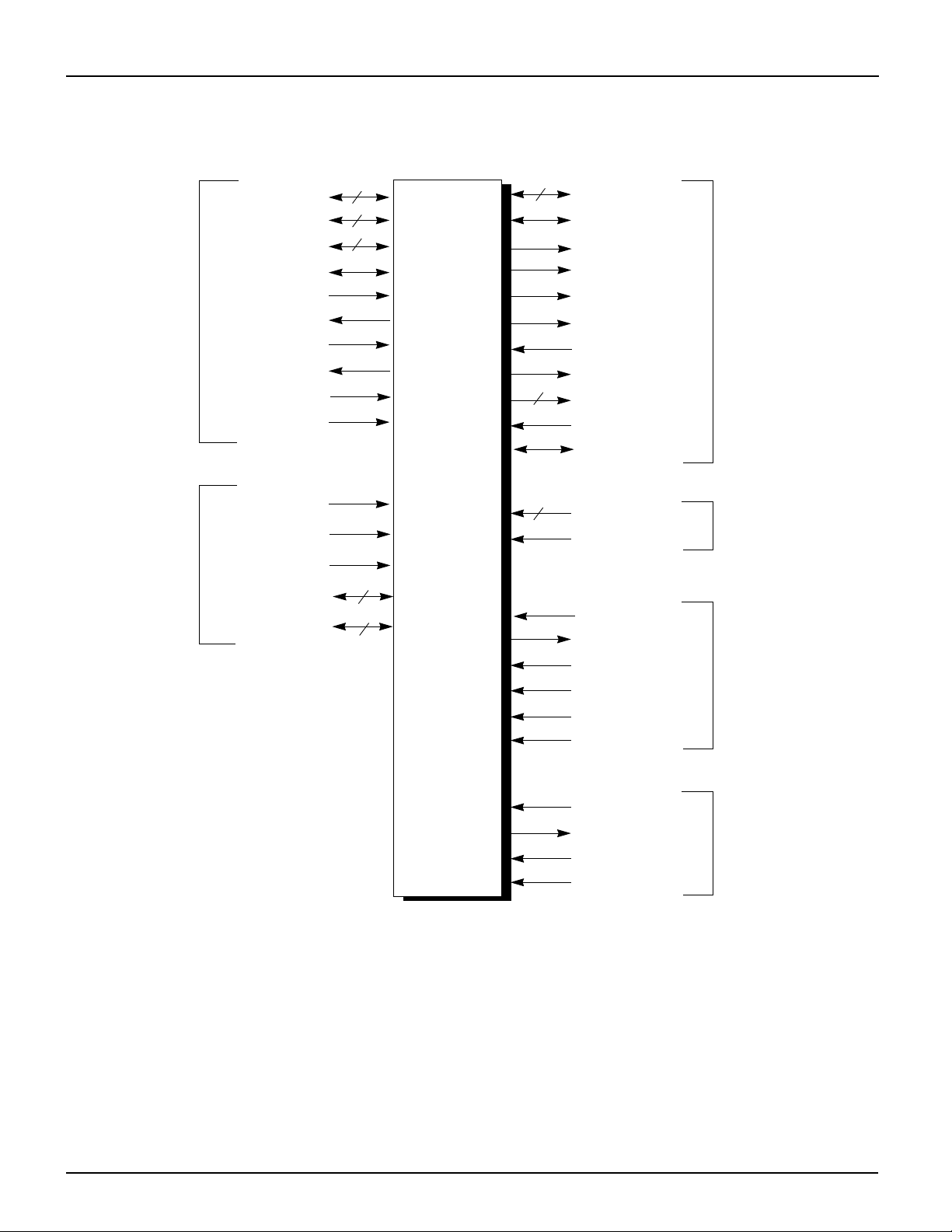
LOGIC SYMBOL
System Interface
Clock Interface
SysAD(63:0)
SysADC(7:0)
SysCmd(8:0)
SysCmdP
ValidIn*
ValidOut*
ExtRqst*
Release*
RdRdy*
WrRdy*
SysClock
VccP
VssP
Vcc
Vss
34
64
34
2
8
9
ScWord (1:0)
ScTCE*
ScTDE*
ScTOE*
ScCLR*
ScDCE*
ScDOE*
ScCWE*
16
ScLine (15:0)
Secondary Cache Interface
ScMATCH
ScVALID
RC5000
Logic
Symbol
6
Int (5:0)*
NMI*
BigEndian
ModeClock
ModeIN
VccOk
ColdReset*
Reset*
Interface
Interrupt
Interface
Initialization
Figure 1. RC5000 Logic Symbol
JTDI
JTDO
JTMS
JTCK
JTAG
Interface
5
Page 6

IDT RC5000 COMMERCIAL TEMPERATURE RANGE
Pin Description
RC5000 implements a bus similar to that of the RC4700. Table 2 lists and describes the RC5000 signals.
Pin Name Type Description
System interface
ExtRqst*
Release*
RdRdy*
WrRdy*
ValidIn*
ValidOut*
SysAD(63:0)
SysADC(7:0)
SysCmd(8:0)
:
Input External Request.
Signals that the system interface needs to submit an external request.
Output Release Interface.
Signals that the processor is releasing the system interface to slave state
Input Read Ready.
Signals that an external agent can now accept a processor read.
Input Write Ready.
Signals that an external agent can now accept a processor write request.
Input Valid Input.
Signals that an external agent is now driving a valid address or data on the SysAD bus and a valid command or data identifier on the SysCmd bus.
Output Valid Output.
Signals that the processor is now driving a valid address or data on the SysAD bus and a valid command or data identifier on the SysCmd bus.
Input/Output System Address/Data bus.
A 64-bit address and data bus for communication between the processor and an external agent.
Input/Output System Address/Data check bus.
An 8-bit bus containing parity check bits for the SysAD bus during data bus cycles.
Input/Output System Command/data identifier bus.
A 9-bit bus for command and data identifier transmission between the processor and an external agent.
SysCmdP
Clock/control inter face:
SysClock
VCCP
VSSP
Interrupt interface:
Int(5:0)*
NMI*
JT AG interface:
JTDI
JTCK
JTDO
Input/Output Reserved System Command/data identifier bus parity.
For the RC5000, unused on input and zero on output.
Input Master Clock.
Master clock input at the bus frequency. The pipeline clock is derived by multiplying this clock up.
Input Quiet VCC for PLL.
Quiet VCC for the internal phase locked loop.
Input Quiet VSS for PLL.
Quiet VSS for the internal phase locked loop.
Input Interrupt.
Six general processor interrupts, bit-wise ORed with bits 5:0 of the interrupt register.
Input Non-maskable interrupt.
Non-maskable interrupt, ORed with bit 6 of the interrupt register.
Input JTAG Data In.
Connected directly to JTDO. No JTAG implemented; should be pulled High.
Input JTAG Clock Input.
Unused input; should be pulled High.
Output JTAG Data Out.
Connected directly to JTDI. If no external scan used, this is a no connect.
Table 2. RC5000 Signal Names and Descriptions (Page 1 of 2)
6
Page 7

IDT RC5000 COMMERCIAL TEMPERATURE RANGE
Pin Name Type Description
JTMS
Initialization interface:
VCCOk
ColdReset*
Reset*
ModeClock
ModeIn
BigEndian
Secondary cache interface:
Input JTAG Command.
Unused input. Should be pulled High.
Input VCC is OK.
When asserted, this signal indicates to the RC5000 that the power supply has been aboveVcc minimum for more than 100 milliseconds and will remain stable. The assertion of VCCOk initiates the reading of the boot-time mode control serial stream.
Input Cold Reset.
This signal must be asserted for a power on reset or a cold reset. ColdReset must be de-asserted synchronously with SysClock.
Input Reset.
This signal must be asserted for any reset sequence. It may be asserted synchronously or asynchronously for a cold reset, or synchronously to initiate a warm reset. Reset must be synchronously deasserted with SysClock.
Output B oot Mode Clock.
Serial boot-mode data clock output at the system clock frequency divided by two hundred and fifty six.
Input Boot Mode Data In.
Serial boot-mode data input.
Input Endian mode select.
Allows the system to change the processor addressing mode without rewriting the mode ROM. If endianness is to be specified by using the BigEndian pin, program mode ROM bit 8 to 0; if endianness is to
be specified by the mode ROM, ground the BigEndian pin.
ScCLR*
ScCWE*(1:0)
ScDCE*(1:0)
ScDOE*
ScLine (15:0)
ScMATCH
ScTCE*
ScTDE*
ScTOE*
ScWord (1:0)
ScValid
Output
Output
Output
Input
Output
Input
Output
Output
Output
Input/Output
Input/Output
Secondary Cache Block Clear.
Clears all valid bits in those Tag RAM’s which support this function.
Secondary Cache Write Enable.
Asserted during writes to the secondary cache
Data RAM Chip Enable.
Chip Enable for Secondary Cache Data RAM
Data RAM Output Enable.
Asserted by the external agent to enable data onto the SysAD bus
Data RAM Output Enable.
Cache line index for secondary cache
Secondary cache Tag Match.
Asserted by Tag RAM on Secondary cache tag match
Secondary cache Tag RAM Chip Enable.
Chip enable for secondary cache tag RAM.
Secondary cache Tag RAM Data Enable.
Data Enable for Secondary Cache Tag RAM.
Secondary cache Tag RAM Output Enable.
Tag RAM Output enable for Secondary Cache Tag RAM’s
Secondary cache Word Index.
Determines correct double-word of Secondary cache Index
Secondary cache Valid.
Always driven by the CPU except during a cache probe operation, when it is driven by the tag RAM.
Table 2. RC5000 Signal Names and Descriptions (Page 2 of 2)
7
Page 8

IDT RC5000 COMMERCIAL TEMPERATURE RANGE
ABSOLUTE MAXIMUM RATINGS
1
RC5000
3.3V±5%
Symbol Rating
V
TERM
Terminal Voltage with
(2)
–0.5
to +4.6 V
UnitCommercial
respect to GND
T
C
Operating Temperature
0 to +85
C
°
(case)
T
BIAS
Case Temperature
–55 to +125
C
°
Under Bias
T
STG
I
IN
I
OUT
NOTES:
1. Stresses greater than those listed under ABSOLUTE MAXIMUM RATINGS may cause permanent damage to the device. This is a stress rating
only and functional operation of the device at these or any other conditions above those indicated in the operational sections of this specification is
not implied. Exposure to absolute maximum rating conditions for extended periods may affect reliability.
minimum = –2.0V for pulse width less than 15ns. VIN should not exceed V
2. V
IN
3. When V
4. Not more than one output should be shorted at a time. Duration of the short should not exceed 30 seconds.
< 0V or VIN > V
IN
CC.
Storage Temperature –55 to +125
DC Input Current 20
DC Output Current 50
(3)
(4)
+0.5 Volts.
CC
C
°
mA
mA
RECOMMENDED OPERATION TEMPERATURE AND SUPPLY VOLTAGE
RC5000
Grade Temperature GND
Commercial 0°C to +85°C (Case) 0V 3.3V±5%
V
CC
8
Page 9

IDT RC5000 COMMERCIAL TEMPERATURE RANGE
AC ELECTRICAL CHARACTERISTICS
(VCC= 3.3V± 5%; T
Clock Parameters—RC5000
= 0°C to +85°C )
case
Parameter Symbol
SysClock HIGH t
SysClock LOW t
SysClock Frequency — 33 90 33 100 33 125 MHz
SysClock Period
SysClock Rise Time t
SysClock Fall Time t
ModeClock Period t
Capacitive Load Deration—RC5000
Parameter Symbol Test Conditions
Load Derate C
LD
180MHz 200MHz
250MHz
†
†#
UnitsMin Max Min Max Min Max
SCHIGH
SCLOW
tSCP
SCRise
SCFall
ModeCKP
3 — 3 — 2.5 — ns
3 — 3 — 2.5 — ns
11.1 30 10 30 8 30 ns
—2.5— 2 — 2ns
—2.5— 2 — 2ns
— 256
t
SCP
180MHz 200MHz
—256
t
SCP
†
—256
250MHz
t
SCP
ns
†#
UnitsMinMaxMinMaxMinMax
— —2—2—2ns/25pF
Power Consumption—RC5000
180MHz 200MHz
Parameter
System Condition 180/45MHz 200/50MHz 250/62.5MHz —
Standby 120mA 120mA 120mA CL = 50 pF
Active 1100mA 1300mA 1800mA C
I
cc
System Interface Parameters—RC5000
Parameter Symbol Test Conditions
Data Output tDM= Min
= Max
t
DO
mode
mode
250MHz
†
†#
ConditionsMax Max Max
= 50pF
L
Pipelined writes or write re-issue
= 25oC
T
c
180MHz 200MHz
= 10 (fastest) 1.5* 7 1.5* 5 1.5* 5 ns
14..13
= 01 (slowest) 1.5* 11 1.5* 11 1.5* 11 ns
14..13
†
250MHz
†#
UnitsMin Max Min Max Min Max
9
Page 10

IDT RC5000 COMMERCIAL TEMPERATURE RANGE
Parameter Symbol Test Conditions
Data Input
t
t
DS
DH
t
t
rise
fall
= 3ns
= 3ns
*Guaranteed by design
Boot Time Interface Parameters—RV5000
Parameter Symbol Test Conditions
Mode Data Setup t
Mode Data Hold t
DS
DH
— 4 —4 —4 —Master Clock Cycle
— 0 —0 —0 —Master Clock Cycle
† Boot Mode Bits 20 and 33 must be set to “1” for operation at this frequency.
# Preliminary information for 250MHz.
180MHz 200MHz
1.5 — 1.5 — 1.5 — ns
0.5 — 0.5 — 0.5 — ns
180MHz 200MHz
†
250MHz
†
†#
250MHz
†#
UnitsMin Max Min Max Min Max
UnitsMinMaxMinMaxMinMax
10
Page 11

IDT RC5000 COMMERCIAL TEMPERATURE RANGE
DC ELECTRICAL CHARACTERISTICS
(Vcc = 3.3V± 5%; T
= 0°C to +85°C)
case
180MHz 200MHz
†
250MHz
Parameter
V
OL
V
OH
V
OL
V
OH
V
IL
V
IH
— 0.1V — 0.1V — 0.1V |I
V
CC
- 0.1V
—V
CC
- 0.1V
—V
CC
- 0.1V
— 0.4V — 0.4V — 0.4V |I
2.4V — 2.4V — 2.4V —
–0.5V 0.2V
0.7V
CC
VCC +
CC
–0.5V 0.2V
0.7V
VCC + 0.5V 0.7V
CC
CC
–0.5V 0.2V
CC
0.5V
I
IN
C
IN
C
IO
C
clk
I/O
LEAK
†
Boot Mode Bits 20 and 33 must be set to “1” for operation at this frequency.
# Preliminary information for 250MHz.
—
10uA —
±
10uA —
±
— 10pF — 10pF — 10pF —
— 10pF — 10pF — 10pF —
— 10pF — 10pF — 10pF
— 20uA — 20uA — 20uA Input/Output Leakage
†#
ConditionsMin Max Min Max Min Max
|= 20uA
OUT
—
|= 4mA
OUT
CC
—
VCC + 0.5V —
10uA 0 ≤ VIN ≤ V
±
CC
11
Page 12

IDT RC5000 COMMERCIAL TEMPERATURE RANGE
PHYSICAL SPECIFICATIONS
The RC5000 is available in two packages, the 223-pin CPGA and the 272-ball SBGA. Infor mation on the CPGA
package is shown in Figure 2 and Table 3; information on the SBGA package is shown in Figure 3 and Table 4.
V
U
T
R
P
N
M
L
K
J
H
223-Pin CPGA
G
F
E
D
C
B
A
1 23456789101112131415161718
Figure 2. RC5000 CPGA Pin Orientation (Bottom View)
12
Page 13

IDT RC5000 COMMERCIAL TEMPERATURE RANGE
223-Pin CPGA Pinout
Pkg
Pin Function
A2 Vcc C5 SysADC[6] E18 Vcc K17 VssP R6 SysAD[51] U9 SysAD[63]
A3 Vss C6 SysAD[16] F1 Vcc K18 Vss R7 SysAD[55] U10 SysAD[13]
A4 Vcc C7 SysAD[50] F2 Reserved L1 Vss R8 SysAD[27] U11 SysAD[11]
A5 Vss C8 SysAD[22] F3 ScValid L2 SysCmd[8] R9 SysAD[31] U12 SysAD[9]
A6 Vss C9 SysAD[24] F4 INT[1]* L3 SysCmd[7] R10 SysAD[43] U13 SysAD[37]
A7 Vcc C10 SysAD[28] F15 ScDCE[0]* L4 SysCmd[5] R11 SysAD[39] U14 SysAD[3]
A8 Vss C11 SysAD[62] F16 ScCWE[0]* L15 ScLine[12] R12 SysAD[35] U15 ScWord[0]
A9 Vcc C12 SysAD[44] F17 ScTDE* L16 ScLine[14] R13 SysAD[1] U16 Vcc
A10 Vss C13 SysAD[10] F18 Vss L17 ScLine[15] R14 ScWord[1] U17 Vss
A11 Vcc C14 SysAD[38] G1 Vss L18 Vcc R15 ScLine[0] U18 Vss
A12 Vss C15 SysAD[4] G2 Reserved M1 Vcc R16 ScLine[3] V1 Vss
A13 Vcc C16 SysAD[34] G3 Reserved M2 SysCmd[6] R17 ScLine[6] V2 Vss
A14 Vss C17 SysAD[2] G4 Reserved M3 SysCmd[4] R18 Vss V3 Vcc
A15 Vss C18 Vss G15 ScCLR* M4 SysCmd[1] T1 Vss V4 Vss
A16 Vcc D1 Vss G16 ScTCE* M15 ScLine[8] T2 SysAD[15] V5 Vss
A17 Vss D2 INT3* G17 ModeIn M16 ScLine[10] T3 SysAD[47] V6 Vcc
A18 Vss D3 INT5* G18 Vcc M17 ScLine[13] T4 SysAD[17] V7 Vss
B1 Vss D4 Release* H1 Vcc M18 Vss T5 SysAD[19] V8 Vcc
B2 Vss D5 Vcc H2 Reserved N1 Vss T6 SysAD[23] V9 Vss
B3 Vcc D6 SysADC[2] H3 Reserved N2 SysCmd[3] T7 SysAD[57] V10 Vcc
B4 SysADC[4] D7 SysAD[48] H4 Reserved N3 SysCmd[2] T8 SysAD[29] V11 Vss
B5 SysADC[0] D8 SysAD[52] H15 VccOK N4 SysADC[7] T9 Vcc V12 Vcc
B6 SysAD[18] D9 SysAD[56] H16 ModeClock N15 ScLine[5] T10 SysAD[45] V13 Vss
B7 SysAD[20] D10 SysAD[60] H17 SysClock N16 ScLine[7] T11 SysAD[41] V14 Vcc
B8 SysAD[54] D11 SysAD[14] H18 Vss N17 ScLine[11] T12 SysAD[7] V15 Vss
B9 SysAD[26] D12 SysAD[42] J1 Vss N18 Vcc T13 SysAD[5] V16 Vss
B10 SysAD[58] D13 SysAD[8] J2 WrRdy* P1 Vcc T14 SysAD[33] V17 Vcc
B11 SysAD[30] D14 SysAD[36] J3 ValidIn* P2 SysCmd[0] T15 Reset* V18 Vss
B12 SysAD[46] D15 ColdReset* J4 ExtReq* P3 SysCmdP T16 ScLine[1]
B13 SysAD[12] D16 SysAD[0] J15 JTDO P4 SysADC[1] T17 Vcc
B14 SysAD[40] D17 ScTOE* J16 JTDI P15 ScLine[2] T18 Vcc
B15 SysAD[6] D18 Vcc J17 JTCK P16 ScLine[4] U1 Vcc
B16 Vss E1 Vss J18 Vcc P17 ScLine[9] U2 Vcc
B17 Vcc E2 INT[0]* K1 Vcc P18 Vss U3 Vss
B18 Vcc E3 INT[2]* K2 ScMatch R1 Vcc U4 SysAD[21]
C1 Vcc E4 INT[4]* K3 RdRdy* R2 SysADC[5] U5 SysAD[53]
C2 Vcc E15 SysAD[32] K4 ScDOE* R3 SysADC[3] U6 SysAD[25]
C3 ValidOut* E16 ScDCE[1]* K15 JTMS R4 BigEndian U7 SysAD[59]
C4 NMI* E17 ScCWE[1]* K16 VccP R5 SysAD[49] U8 SysAD[61]
Pkg
Pin Function
Pkg
Pin Function
Table 3. 223-Pin CPGA Pinout
Pkg
Pin Function
Pkg
Pin Function
Pkg
Pin Function
13
Page 14

IDT RC5000 COMMERCIAL TEMPERATURE RANGE
192021
123456789101112131415161718
A
B
C
D
E
F
G
H
J
K
272-Ball SBGA
L
M
N
P
R
T
Figure 3. Ball Grid Array Package (Bottom View)
U
V
W
Y
AA
14
Page 15

IDT RC5000 COMMERCIAL TEMPERATURE RANGE
272-Ball SBGA Pinout
Pkg
Pin Function
AA1 Vss B5 SysAD0 D9 Vss J2 SysAD46 P21 SysAD55 W1 Vss
AA2 Vcc B6 ScTOE* D1 0 Vcc J3 SysAD14 R1 Vss W2 Vcc
AA3 Vss B7 ScCLR* D11 Vccp J4 Vss R2 SysAD18 W3 Vcc
AA4 ValidOut* B8 ScTDE* D12 Vcc J18 Vss R3 SysAD48 W4 Vcc
AA5 Vss B9 ModeClock D13 Vss J19 SysAD9 R4 Vcc W5 Int*5
AA6 Int*0 B10 JTDI D14 Vcc J20 SysAD41 R18 Vcc W6 Int*4
AA7 Vss B11 JTCK D15 Vcc J21 Vss R19 SysAD53 W7 Int*1
AA8 Reserved B12 N/C D16 Vss K1 SysAD60 R20 SysAD23 W8 Reserved
AA9 Vss B13 ScLine14 D17 Vcc K2 SysAD30 R21 Vss W9 Reserved
AA10 WrRdy* B14 ScLine10 D18 Vss K3 SysAD62 T1 SysAD16 W10 Reserved
AA11 Vss B15 ScLine9 D19 Vcc K4 Vcc T2 SysADC0 W11 ValidIn*
AA12 ScMatch B16 ScLine6 D20 Vcc K18 Vcc T3 SysADC2 W12 ScDOE*
AA13 Vss B17 ScLine3 D21 Vcc K19 SysAD11 T4 Vss W13 SysCmd7
AA14 SysCmd6 B18 ScLine1 E1 Vss K20 SysAD43 T18 Vss W14 SysCmd4
AA15 Vss B19 Vcc E2 SysAD36 K21 SysAD13 T19 SysAD19 W15 SysCmd1
AA16 SysCmd2 B20 Vcc E3 SysAD4 L1 Vss T20 S ysAD51 W1 6 SysADC7
AA17 Vss B 21 Vcc E4 Vcc L2 SysAD58 T21 SysAD21 W17 SysADC5
AA18 SysADC3 C1 Vss E18 V cc L3 SysAD28 U1 Vss W18 SysAD47
AA19 Vss C2 Vcc E19 ScWord1 L4 Vcc U2 SysADC4 W19 BigEndian
AA20 Vcc C3 ColdReset* E20 ScWord0 L18 Vcc U3 SysADC6 W20 Vcc
AA21 Vss C4 SysAD34 E21 Vss L19 SysAD45 U4 Vcc W21 Vss
A1 Vss C5 ScDCE*1 F1 SysAD8 L20 SysAD63 U18 Vcc Y 1 Vcc
A2 Vcc C6 ScDCE*0 F2 SysAD38 L21 Vss U19 SysA D1 7 Y2 Vcc
A3 Vss C7 ScCWE*0 F3 SysAD6 M1 SysAD26 U2 0 SysAD49 Y3 Vcc
A4 SysAD32 C8 ScTCE* F4 Vss M2 SysAD56 U21 Vss Y4 Release*
A5 Vss C9 ModeIn F18 Vss M3 SysAD24 V1 Vcc Y5 Int*3
A6 ScCWE*1 C10 JTDO F19 SysAD1 M4 Vcc V2 Vcc Y6 Int*2
A7 Vss C11 Vssp F20 SysAD33 M18 Vcc V3 Vcc Y7 ScValid
A8 VCCOK C12 JTMS F21 SysAD3 M 19 SysAD29 V4 Vss Y8 Reserved
A9 Vss C13 ScLine13 G1 Vss M20 SysAd61 V5 NMI* Y9 Reserved
A10 MasterClk C14 ScLine11 G2 SysAD10 M21 SysAD31 V6 Vss Y10 Reserved
A11 Vss C15 ScLine8 G3 SysAD40 N1 Vss V7 Vcc Y11 ExtRqst*
A12 ScLine15 C16 ScLine5 G4 Vcc N2 SysAD54 V8 Vcc Y12 RdRdy*
A13 Vss C17 ScLine4 G18 Vcc N3 SysAD22 V9 Vss Y 13 SysCmd8
A14 ScLine12 C18 ScLine0 G19 SysAD35 N4 Vss V10 Vcc Y14 SysCmd5
A15 Vss C19 Reset* G20 SysAD5 N18 Vss V11 Vcc Y15 SysCmd3
A16 ScLine7 C20 Vcc G21 Vss N19 SysAD27 V12 Vcc Y16 SysCmd0
A17 Vss C21 Vss H1 SysAD42 N20 SysAD59 V13 Vss Y17 SysCmdP
A18 ScLine2 D1 Vcc H2 SysAD44 N21 Vss V14 Vcc Y18 SysADC1
A19 Vss D2 Vcc H3 SysAD12 P1 SysAD50 V15 Vcc Y19 SysAD15
A20 Vcc D3 Vcc H4 Vcc P2 SysAD52 V16 Vss Y20 Vcc
A21 Vss D4 Vss H18 Vcc P3 SysAD20 V17 Vcc Y21 Vcc
B1 Vcc D5 Vcc H19 SysAD7 P4 Vcc V18 Vss
B2 Vcc D6 Vss H20 SysAD39 P18 Vcc V19 Vcc
B3 Vcc D7 Vcc H21 SysAD37 P19 SysAD25 V20 Vcc
B4 SysAD2 D8 Vcc J1 Vss P20 SysAD57 V21 Vcc
Pkg
Pin Function
Pkg
Pin Function
Pkg
Pin Function
Pkg
Pin Function
Pkg
Pin Function
Table 4. 272-Ball SBGA Pinout
15
Page 16

IDT RC5000 COMMERCIAL TEMPERATURE RANGE
ORDERING INFORMATION
IDT79 YY XXXX 999 A A
Operating
Voltage
Device
Type
Speed Package Temp range/
Process
Blank Commercial
G
BS
180
200
250
5000
RV
(0°C to +85°C Case)
223-pin CPGA
272-pin SBGA
180 MHz PClk
200 MHz PClk
250 MHz PClk
Multi-Issue
64-bit Microprocessor
3.3+/-5%
VALID COMBINATIONS
IDT79RV5000 - 180, 200MHz G CPGA package
IDT79RV5000 - 180, 200, 250MHz BS SBGA package
Integrated Device Technology, Inc. reserves the right to make changes to the specifications in this data sheet in order to improve design or performance and to supply the best possible product.
Integrated Device Technology, Inc.
2975 Stender Way, Santa Clara, CA 95054-3090 Telephone: (408) 727-6116 FAX 408-492-8674
16
 Loading...