

Page 1
RC7352
Parametric Measurement Unit
www.fairchildsemi.com
Features
• Force voltage/measure current and force current
measure voltage functions
• Forced voltage range (-5V to +15V)
• Four programmable measured current ranges:
Range A = ±20mA max
Range B = ±200mA max
Range C = ±1.0mA max
Range D = ±40mA max
• High resolution current force/measure ±0.05% = 2 bits
• Internal control circuitry for selecting ranges
• High accuracy: 12 bit linearity and 0.5% gain error
• High current range D current limit protection set
externally by the value of resistor R
DIL
• Measurement output voltage can be disabled
• Forced current ranges:
Range A = ±20mA max
Range B = ±200mA max
Range C = ±1.0mA max
Range D = ±40mA max
• Measured voltage range: -5V to +15V
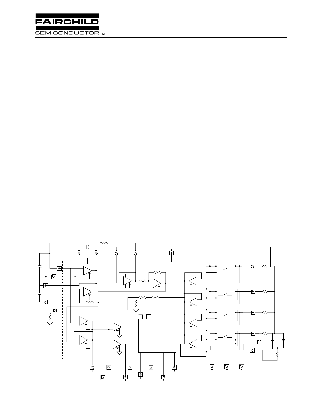
Block Diagram
• High resolution voltage measurement (±0.05%) and
accuracy: (±10mV max. offset) and 0.5% gain error
• Internal current limit for ranges (A, B, & C)
Applications
• ATE pin electronics measurements
• Instrumentation, meters
• Programmable voltage or current supply
Description
The RC7352 is a “Per Pin” Parametric Measurement Unit
(PMU) that can force voltage and measure current or force
current and measure voltage. The RC7352 forces voltages
from +15V to -5V when +V
currents up to ±40mA. All logic inputs for the RC7352 are
TTL compatible, while the open collector logic outputs are
TTL/CMOS compatible.
Setting the SI/V (Select I/V) pin low puts the RC7352 in
the force voltage and measure current mode. The resulting
output voltage at the DUT matches the input applied to the
is 20V and –VS is -10V, or
S
VIN
17
CAP
11
CAP_I
23
I/VIN
RADJ
18
CAP_V
10
V/I FORCE
V/I MEAS.
6
CA
+
–
+
–
+
–
+
–
+
–
+
I
–
V
+
–
+
I
–
I
I
V
I
I
25
CB
WINDOW
COMPARATOR
26
I/V MN
4
I/V MX
15
I/V M
+
–
+
–
+
–
+
–
I
7
I/VOUT
+
–
+
E
E
–
5
VHS
I SENSE
I
27
VLS
20
VFB
I
I: FI/MV
V: FV/MI
13
SI/V
+
–
+
V
LOGIC
BIAS
12
RS1
28
+VS
(20V)
4:1 MUX
–
–
A = 4
I
–
&
21
VDIS
14
RS2
+
I
+
–
–
+
I
+
–
–
+
I
+
–
–
+
I
+
/4
RANGE A
IN
EN
RANGEA.SCH
RANGE B 19
IA
IB
IC
ID
IN
EN
RANGEB.SCH
RANGE C 22
IN
EN
RANGEC.SCH
RANGE D 24
IN
EN
RANGED.SCH
8
GND
OUT
OUT
OUT
OUT
RDIL
D2
16
-VS
(-10V)
RDIL
3
VEE
(-10V)
9
R
A
R
B
R
C
R
1
D
D
2
65-7352-01
Rev. 1.1.2
Page 2
RC7352 PRODUCT SPECIFICATION
I/VIN pin (please refer to block diagram). The I/VM pin
provides a voltage proportional to the DUT current.
V(I/VM) = (4 x R x I(DUT)), where R is the external range
resistor (0.05% tolerance) and I(DUT) is the current supplied to the load. The resistors in the application circuit were
chosen using this formula R range = (2V/Imax), for Range A
this is RA = 2/20 mA or 100K.
When SI/V is high the RC7352 will force current and
measure voltage. The range select pins RS1 and RS2 control
the maximum output current (see Table 1), while magnitude
of the forced current is given by the expresion
I(DUT) = V(I/VIN)/(4 x R)
where R is the range resistor. In the FI/MV mode the v oltage
at the I/VM pin equals the device voltage. The I/VM pin can
be connected to an A/D convertor to monitor the current or
voltage at the load device.
The RC7352 also has a window comparator that can provide
upper or lower limit fail information. I/Vmx and I/Vmn are
voltage inputs for the upper and lower limits respectively.
You must use the formulas listed above to calculate current
limits for each range while voltage limits are 1:1. Their
corresponding outputs, VHF (V high fail) and VLF (V low
fail) can be used individually or “Wire ORed” to obtain a
composite signal. Additionally the VDIS pin can be set high
to disable the window comparator and its I/O lines. Although
this reduces overall power consumption, it also disables the
I/VM output.
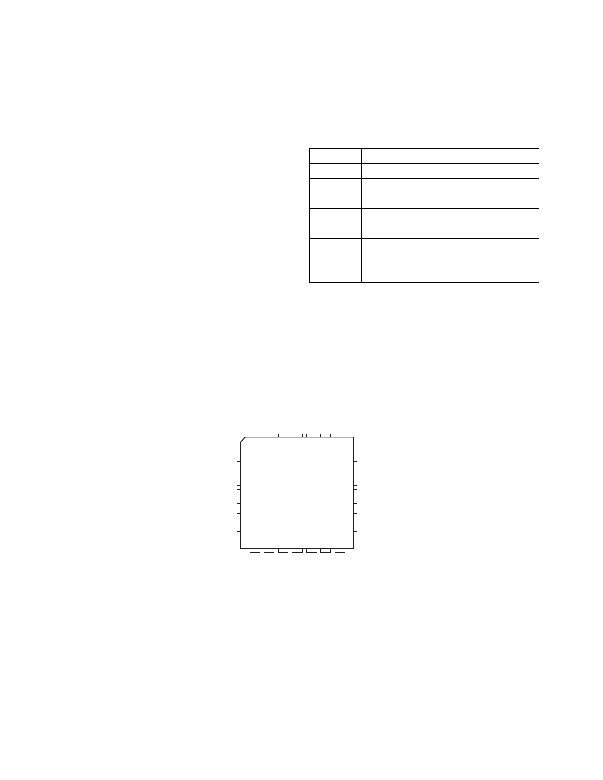
Table 1. Maximum Output Current on
Pin Select
SI/V RS2 RS1 Mode
0 0 0 FV/MI Range A, Imax = ±20 mA
0 0 1 FV/MI Range B, Imax = ±200 mA
0 1 1 FV/MI Range C, Imax = ±1.0 mA
0 1 0 FV/MI Range D, Imax = ±40 mA
1 0 0 FI/MV Range A, Imax = ±20 mA
1 0 1 FI/MV Range B, Imax = ±200 mA
1 1 1 FI/MV Range C, Imax = ±1.0 mA
1 1 0 FI/MV Range D, Imax = ±40 mA
Notes:
1. FV/MI = Force Voltage Measure Current.
2. FI/MV = Force Current Measure Voltage.
3. +V
–5 ³ V
S
OUT
³ –VS+5
Pin Assignments
V
HF
C
IV
OUT
GND
R
RADJ
CAP_I
MX
VEER
I/V
4 3 2 1 28 27 26
5
6
A
7
8
9
A
10
11
12
RC7352
13 14 15 16 17 18
1
RS
RS
SI/V
DIL
2
D
+VSVLFI/V
–V
I/VM
MN
25
C
B
24
R
D
23
I/V
IN
22
R
C
21
V
DIS
20
V
FB
19
R
B
S
CA
65-7352-02
CAP_V
2
Page 3
PRODUCT SPECIFICATION RC7352
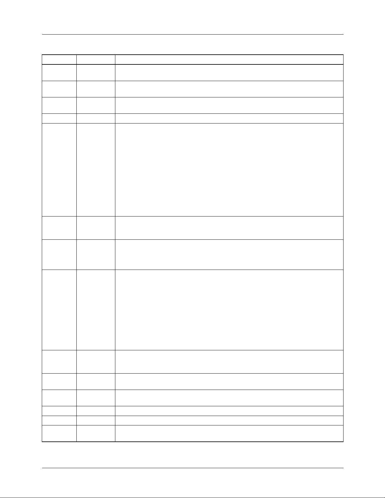
Pin Description
Pin Name Pin Number Pin Description
+V
S
-V
S
V
EE
GND 8 This pin should be connected to the printed circuit board’s ground plane.
I/V
IN
28 +VS should be bypassed to ground with a 10.0 mF tantalium capacitor placed as
close to the pin as possible.
16 –VS should be bypassed to ground with a 10.0 mF tantalium capacitor placed as
close to the pins as possible.
3V
is the negative supply for range D. This pin should be bypassed with a 0.1 mF
EE
ceramic capacitor to ground.
23 Input reference voltage for V
OUT
or I
. In the force voltage measure current mode
OUT
(FV/MI)
V(I/V
) = V(I/VIN )
OUT
and
V(I/VM) = 4 x I
Where I
OUT
x R
OUT
is the device output current and R is the range resistor.
In the Force Current/Measure Voltage Mode
V I VIN¤()
------------------------=
4R´
)
OUT
. The current to the load is
OUT
serving as the voltage
OUT
I/V
OUT
I
OUT
V(I/VM) = V(I/V
7 The Load or Device under test is connected to I/V
supplied via the appropriate range resistor with I/V
feedback point for the PMUs internal instrumentation amplifier.
SI/V 13 A TTL/CMOS signal applied to this pin selects either Force Voltage/Measure Current
or Force Current/Measure Voltage mode. A TTL/CMOS low level will select Force
Voltage/Measure Current function. A TTL/CMOS high level selects Force Current/
Measure Voltage mode.
R
A
9 Resistor RA should be placed between RA and I/V
. RA tolerance should be
OUT
better than +0.05% to improve gain error. Maximum current for range A is shown in
the equation below.
2V±
I
---------- -=
A
R
A
The ±2 volts represents the maximum voltage VA across RA. For Range A, IA should
not exceed ±20 mA, i.e., RA should be higher than or equal to 100 kW. A metal film
resistor should be used to reduce inherent resistor noise (schott and pop corn noise)
and improve resolution. For maximum stability, a 300 pF capacitor should be
connected across RA.
R
B
19 For Range B, IB should not exceed ±200 mA, i.e., RB should be higher than or equal
to 10 kW with ±0.05% tolerance. For maximum stability a 1,000 pF capacitor should
be connected across RB.
R
C
22 For Range C, IC should not exceed ±1 mA, i.e., RC should be higher than or equal to
2 kW with ±0.05% tolerance.
R
D
24 For Range D, ID should not exceed ±40 mA, i.e., RD should be higher than or equal
to 50 W with ±0.05% tolerance.
D 1 Two diodes must be connected between D & R
, C
C
A
B
R
DIL
6, 25 A 30pF capacitor placed between these pins will improve stability.
2 Range D output for current limiting. An external resistor is connected between RDIL
and D to limit current to a value I
= 0.8V/RLM.
LIM
as shown in the block diagram.
D
3
Page 4
RC7352 PRODUCT SPECIFICATION
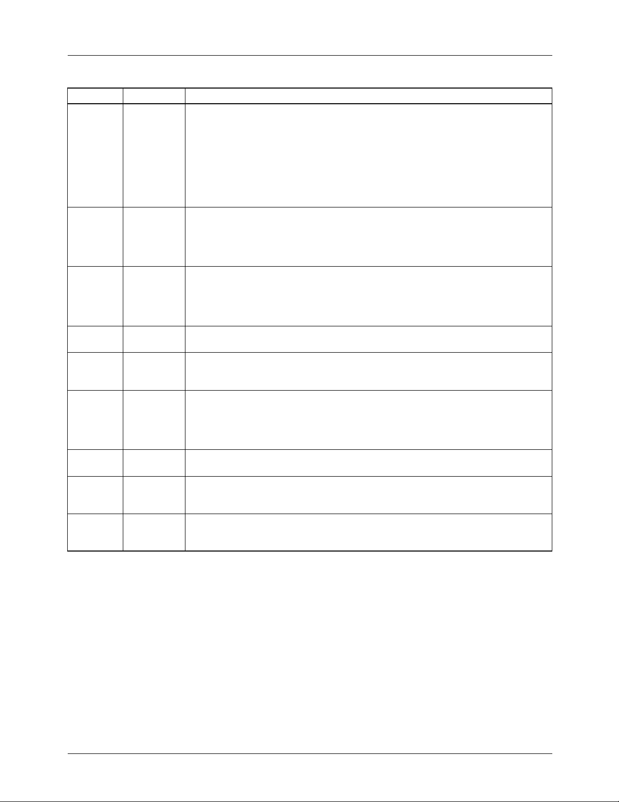
Pin Description (continued)
Pin Name Pin Number Pin Description
RS1, 12 RS1 and RS2 are TTL or CMOS compatible. The truth table below shows the range
selection table.
R
S2
I/VMX,
I/V
MN
V
HF
V
LF
V
DIS
I/VM 15 In the Force Voltage/Measure Current mode this output voltage is equal to four times
V
FB
RADJ 10 The RADJ pin is provided to adjust the offset for the I
CAP_I
CAP_V
CA
14 RS1 RS2 Range Selected
LL A
L H B
H H C
H L D
4
26
The voltage applied to pin 4 sets the upper current or voltage limit for the
measurement at pin 15 I/VM. To set the desired limit for current measurement a
voltage equaling (4 x I
x R) must be applied on this pin. R is the external resistor of
L
the selected range (A, B, C, or D). For voltage measurement the voltage applied to
this pin is the limit.
5V
, High Fail, is an open collector output that requires a pull-up to the logic supply.
HF
If the voltage at pin 15, I/VM, is greater than the threshold voltage at pin 4, I/VMX,
VHF will become a logic low. The open collector structure makes wire-ORing of
multiple PMU’s possible. Connect a 3,000 pF capacitor to GND to minimize
oscillation at the cross-over point.
29 VLF mirror VHF for the lower threshold I/VMN. Connect a 3,000 pF capacitor to GND
to minimize oscillation at the cross over point.
21 When V
is tied to ground output I/VM, VHF and VLF are enabled. If V
DIS
DIS
is open
VHF and VLF will require external pullups to maintain a logic high. And I/VM will be in
a high impedance state.
the voltage across external resistor R of selected range A, B, C, or D through which
the measured current is flowing ((I/V)M = 4.0 x IM x R). In the Force Current/
Measure Voltage mode this output is equal to the voltage at I/V out. This output can
be disabled by applying a TTL HI on the V
20 VFB, voltage feedback, is the buffered output voltage, I/V
pin. (Pin 21)
DIS
. This pin should not
OUT
be loaded. Connect a 50K 1% resistor from VFB to CAP_V.
function. The best
SENSE
accuracy for V/IM is obtained when RADJ is shorted to analog ground. The point is
terminated with a 100 W resistor in the block diagram.
11
18
17
CA is the common point for two 50 pF compensation capacitors that improve the
stability of the PMU. These components are optional and can be omitted for some
loads.
4
Page 5
RC7352 PRODUCT SPECIFICATION
Absolute Maximum Ratings
1
Parameter Min. Max. Units
Absolute Difference, +VS+|–VS| 32 V
Digital Control Inputs
SI/V, RS1, RS2, V
DIS
-2 +6 V
Comparator Inputs
I/VMN, I/VMX I/V
I/V
IN
Notes:
1. Absolute maximum ratings are limiting values applied individually while all other parameters are within specified operating
conditions. Functional operation under any of these conditions is NOT implied.
2. Applied voltage must be current limited to specified range, and measured with respect to GND.
3. Forcing voltage must be limited to specified range.
4. Current is specified as conventional current flowing into the device.
£ +V
MN
S
–VS £ I/V
–VS £I/V
+V
S
IN
MX
V
£
V
Recommended Operating Conditions
Symbol Parameters Min. Typ. Max. Units
T
C
+V
S
–VS
V
EE
R
A
R
B
R
C
R
D
Notes:
1. +V
+ |–VS| £ 30V +VS + |–VS| ³ 24
S
2. –V
& VEE are always at the same voltage.
S
Case operating temperature 0 70 °C
Positive supply voltage
Negative supply voltage
Negative supply voltage for range D
1
1
2
10.4 20.0 20.6 V
-15.75 -10.0 -9.5 V
–V
S
V
Resistor for IA current range 100 2000 KW
Resistor for IB current range 10 200 KW
Resistor for IC current range 2 40 KW
Resistor for ID current range 50 1000 W
5
Page 6
PRODUCT SPECIFICATION RC7352
DC Electrical Characteristics
+VS = 20V ±3%, –VS = -10V ±5% TA = 25°C, and external ±0.05% tolerance resistors RA = 1000kW, R
R
= 2kW, and R
C
= 50W unless otherwise specified.
D
Symbol Parameters Test Conditions Min. Typ. Max. Units
Forced Current/Measure Voltage
I/V
IN
I/V
M
V
MR
V
OR
V
GE
CMRR
I
OER
Input Voltage Range For Setting
Forced Current (I
)
F
= 4 x IF x R -8 +8 V
I/VF
IN
Measured Voltage Output @ (I/V)M All ranges, full scale current -5 +15 V
Output Sink/Source Current (I/V)
= -5V, +15V -200 +200 mA
M
Voltage Measured Resolution -.05 ±0.025 +0.05 %FSR
Voltage Measurement Offset I/VIN = 0V; Measured @ I/VM -6.0 ±2 +6.0 mV
Voltage Gain Error Gain of 4 -2.0 +0.5 +2.0 %
1
I
Error Due to Common Mode
OUT
Load Voltage
-5V £ I/V
@ (I/V)
£ +15V; Measured
OUT
M
45 60 dB
Forced Voltage/Measure Current
I/V
I/VF
IN
VOS
Force Input Voltage Range All ranges, full scale current -5 +15 V
Forced Voltage Offset I/VIN = 0V, measure I/V
OUT
and
-6.0 ±2 +6.0 mV
VFB
Forced Voltage Linearity Error ±0.025 ±0.05 FSR%
2
CMRR
VLER
I/V
OUT
I/V
M
I
Measure Error Due to I/VM
OUT
Common Mode Voltage
-FSR £ I
@ (I/V)
£ +FSR; Measured
OUT
M
45 60 dB
Forced Output Voltage Range All ranges, full scale current -5 +15 V
Voltage Output Equivalent to
All ranges, full scale voltage -8 +8 V
Measured Current:
= 4 x IF x R
(I/V)
M
I I measured; I = (I/
)/(4R) I/VM = -8.0V, +8.0V; full scale -200 +200 mA
VM
Current Ranges
Range A
I
A
I
AMR
I
LIN
l
GE
I
FIOS
I
MIOS
Maximum Full Scale Current RA = 100kW (0.05%) ±20 mA
Current Measurement Resolution guaranteed by design ±0.025 %
Linearity
Current Gain Error
Force Current Offset
Measure Current Offset
3
4
5
6
I/VIN = 0V -25 ±10 +25 nA
I/VIN = 0V -25 ±10 +25 nA
-0.05 ±0.025 +0.05
-2.0 0.5 +2.0 %
Range B
I
B
I
BMR
I
LIN
l
GE
I
FIOS
I
MIOS
Maximum Full Scale Current RB = 10kW (0.05%) ±200 mA
Current Measurement Resolution guaranteed by design ±0.025 %
Linearity
Current Gain Error
Force Current Offset
Measure Current Offset
3
4
5
6
-0.05 ±0.025 +0.05
-2.0 ±0.5 +2.0 %
-250 ±100 +250 nA
-250 ±100 +250 nA
= 10kW,
B
6
Page 7
RC7352 PRODUCT SPECIFICATION
DC Electrical Characteristics (continued)
Symbol Parameters Test Conditions Min. Typ. Max. Units
Range C
I
C
I
CMR
I
LIN
l
GE
I
FIOS
I
MIOS
Range D
I
C
I
DMR
I
LIN
l
GE
I
FIOS
I
MIOS
Digital Control Inputs (SI/V, RS1, RS2)
V
IH
I
LH
I
LL
Digital Control Input V
V
IH
I
LH
I
LL
Comparator Input; I/V
I/V
MX,MN
I
H
I
L
Comparator Status Outputs; VHF, V
V
OH
V
OL
I
OH
I
OL
I
Z
Other
I+ (1.0) Positive Supply Current No load Range A 4.0 11.0 mA
I- (2.0) Positive Supply Current No load Range A 4.0 11.0 mA
Notes:
1. CMRR is measured with V
due to the V
CMRR 20
Maximum Full Scale Current RC = 2kW (0.05%) ±1mA
Current Measurement Resolution guaranteed by design ±.025 %
Linearity
Current Gain Error
Force Current Offset
Measure Current Offset
3
4
5
6
-0.05 ±.025 +0.05 %
-2.0 ±0.5 +2.0 %
-1.5 ±0.5 +1.5 mA
-1.5 ±0.5 +1.5 mA
Maximum Full Scale Current RD = 50W (0.05%) ±40 mA
Current Measurement Resolution
guaranteed by design ±.025 %
Current Measurement Accuracy
Linearity
Current Gain Error
Force Current Offset
Measure Current Offset
3
4
5
6
-0.05 ±.025 +0.05 %
-2.0 ±0.5 +2.0 %
-50 ±20 +50 mA
-50 ±20 +50 mA
Internal Threshold Voltage 0.8 1.4 2.0 V
Logic High Bias Current VH = 2.0V 200 nA
Logic Low Bias Current VL = 0.8V 2.0 nA
DIS
Internal Threshold Voltage 0.8 1.4 2.0 V
Logic High Bias Current VH = 2.0V 1.0 mA
Logic Low Bias Current VL = 0.8V 2.0 nA
, I/V
MAX
MIN
Input Voltage Range -8.0 +15 V
Input Bias Current (Logic High) VH = +15V 0.4 mA
Input Bias Current (Logic Low) VL = 0.8V 0.4 mA
LF
Output Voltage (Logic High) R
Output Voltage (Logic Low) R
Output Current High V
PULLUP
PULLUP
OUT
= 10kW 3.5 V
= 10kW 0.8 V
= 5.0V 0.1 mA
Output Current Low 1.0 mA
Output Leakage Current Disable State V
=15V/-5V; R is RA, RB, RC or RD; V1 = constant; This parameter is to define the I
OUT
DV
L
4´ R´
L
common mode voltage for a constant V1. This parameter is guaranteed to full V1 range. (±8V)
L
DI
æö
log=
------------------------------------- -
ç÷
èø
= 5.0V 0.1 mA
OUT
OUT
current error
7
Page 8
RC7352 PRODUCT SPECIFICATION
I
OUT
R
V
L
I/V
I/V
IN
V
1
OUT
FI/MV
I/V
M
65-7352-03
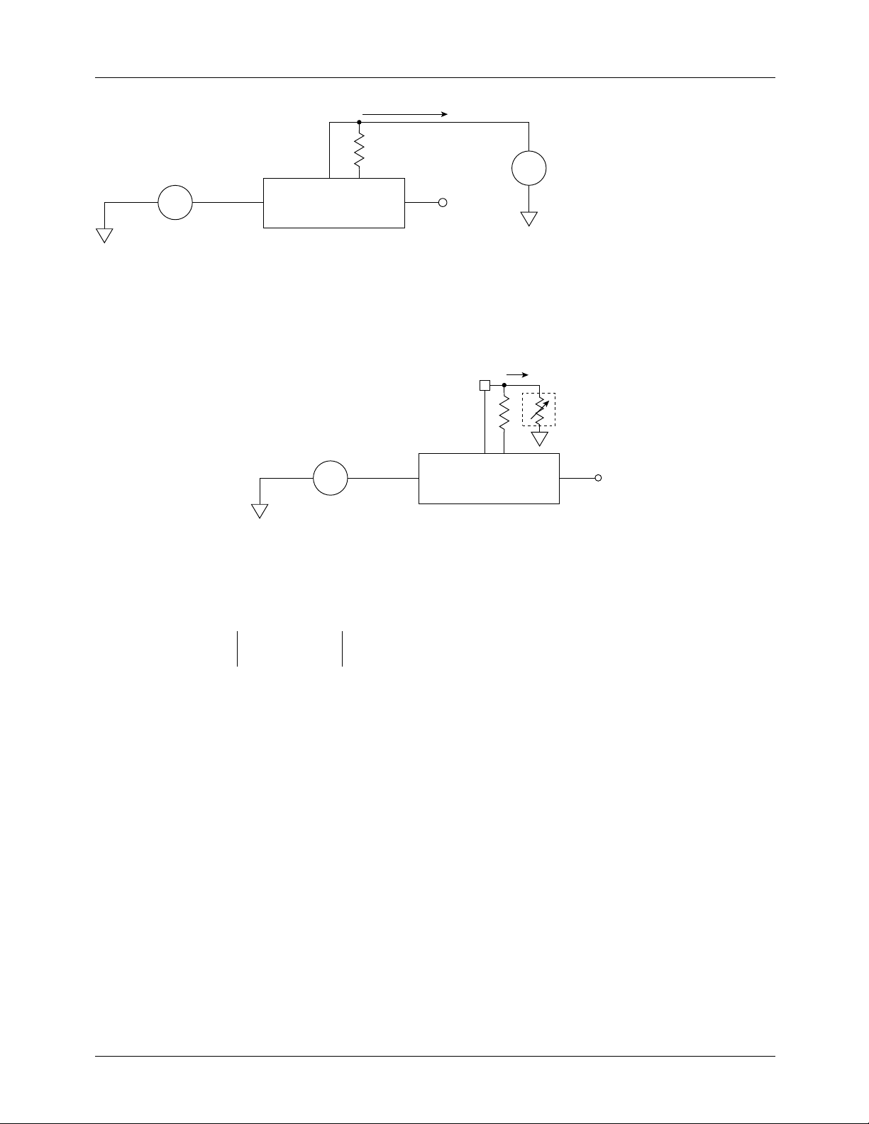
2. CMRR is measured with V1 = +15V/-5V; R is RA, RB, RC or RD; I
measurement error due to the input voltage V
DV
æö
CMRR 20
log=
------------
ç÷
DV
èø
M
1
65-7352-04
. It guarantees all ranges and ± full scale I
1
I/V
IN
V
1
= constant. This parameter is to define the current
OUT
I/V
FV/MI
R
OUT
I
OUT
I/V
R
M
.
OUT
L
V
M
3. Linearity is measured against two point straight line calibration with five measurement points.
4. Current Gain Error is measured with –full scale current to +full scale current. The ideal gain is 4.
VM
VM1–
Current Gain Error
=
2
------------------------------------------------- RI
–()
OUT2IOUT1
5. Force current is measured with I/V
to ground with I/VIN = 0V.
OUT
6. Measured current offset is measured with I/V
8
= 0V, Offset = (I/VM)/4R where R is RA, RB, RC, and RD.
IN
Page 9
PRODUCT SPECIFICATION RC7352
AC Electrical Characteristics
+VS = 20V ±3%, -VS = -10V ±5%, TA = 25°C, and external ±0.05% tolerance resistors RA = 100kW,
RB = 10kW, RC = 2kW, and RD = 50W unless otherwise specified.
Symbol
Parameters Test Conditions Min. Typ. Max. Units
Comparator
t
HL
t
LH
Response Time High to Low R
Response Time Low to High R
Differential Amplifier
t
MZF
Response Time (setting time)
Force Current/Measure Voltage Range B 2.3
t
MZF
Response Time (settling time)
Force Voltage/Measure Current Ranges B 2.5
t
MZF
t
DS
Response Time (Settling time)
Output Disable to Enable Time 20 ms
= 10k, 5mV Overdrive 1.1 ms
LOAD
= 10k, 5mV Overdrive 450 ns
LOAD
1
Range A 2.4 ms
Range C 2.6
Range D 2.6
Voltage @ I/V
I
= Max
F
1
Ranges A 2.4 ms
= -5.0V to +15V
M
Ranges C 2.6
Ranges D 2.7
Voltage @ I/V
I
= Max
M
1
Ranges A, B, C, & D 1.0 3 ms
Voltage @ I/V
= 5.0V to +15V
OUT
= -2.0V to +6.0V
OUT
30pF from CA to CB
No Load
Notes:
1. Response Time (settling time) for Force Current/Measure Voltage mode is measured with 30pF from CA to CB and
I/V
Voltage Swings from -8.0V to +8.0V, and RL value for Range placed between I/V
IN
500KW A
50KW B
10KW C
250W D
OUT
and 5V.
9
Page 10
RC7352 PRODUCT SPECIFICATION
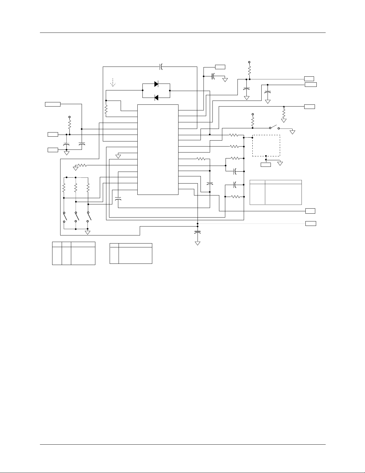
Application Example
I/VMX
VHF
GND
VOUT UPPER LIMIT
5V
R13
100K
VOUT HIGH FAIL
C5
3nFC11nF
R17
¨
100
5V
R9
R8
100K 100K 100K
RS1
SI/V
RS2
R12
50
R11
2K
R10
10K
C3
1nF
C9
300pF
R6
100K
5V
5V
R13
100K
C7
3nF
*
R13
100K
DUT or
VDIS
L
H
LOAD
GND
VOUT LOW FAIL
VOUT LOW LIMIT
C8
1nF
R18
100K
*
S1
DUT GND
VHS VLS I/VM
OUTPUTS
ENABLED
OUTPUTS
DISABLED
VOLT/CURRENT
MEASUREMENT
I/VIN
VLF
I/VMN
I/VIN
V/IM
-VS
R16
50K
VPOS
C2
6.8uF
+20V
C6
6.8uF
+VS
*
CV
50pF
C4 *
RANGE D CURRENT LIMIT
1
2
3
4
5
6
7
8
9
10
11
12
13
14
*
CI
50pF
X0
D1&2
RDIL
VEE
I/VMX
VHF
CA
I/VOUT
GND
RA
RADJ
CAP_I
RSI
SI/V
RS2
R15
16
R7
1pF
D1
1N4148
D2
1N4148
+VS
VLF
I/VMN
CB
RD
I/VIN
RC
VDIS
VFB
RB
CAP_V
CAP
-VS
V/IM
28
27
26
25
24
23
22
21
20
19
18
17
16
15
VNEG
-10V
RS1 RS2 RANGE
L L A +/-20uA
L H B +/-200uA
H H C +/-1mA
H L D +/-40mA
FUNCTIONSI/V
L FORCE VOLTAGE
H FORCE CURRENT
* OPTIONAL PART
¨ SHORT RADJ TO GND FOR BEST DC ACCURACY
65-7352-05
10
Page 11
PRODUCT SPECIFICATION RC7352
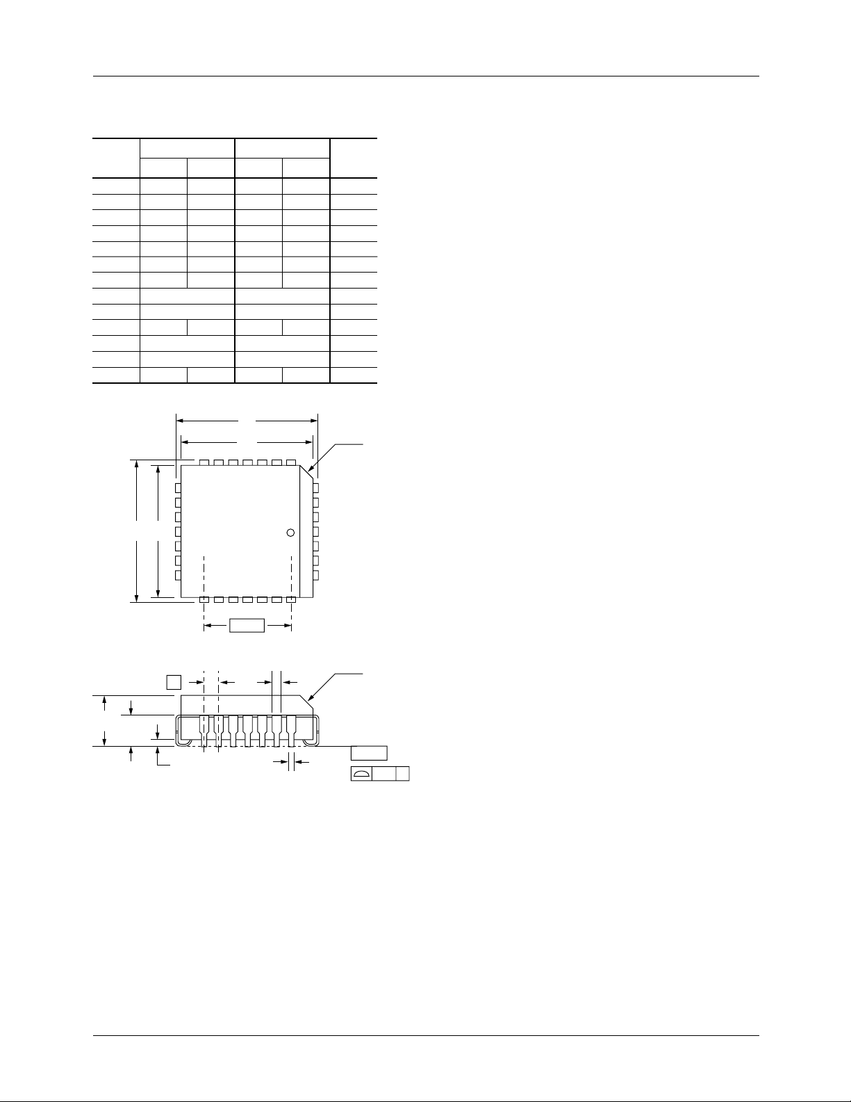
Mechanical Dimensions
Symbol
A .165 .180 4.19 4.57
A1 .090 .120 2.29 3.05
A2 .020 .51——
B .013 .021 .33 .53
B1 .026 .032 .66 .81
D/E .485 .495 12.32 12.57
D1/E1 .450 .456 11.43 11.58
D3/E3 .300 BSC 7.62 BSC
e .050 BSC 1.27 BSC
J .042 .048 1.07 1.22 2
ND/NE 7 7
N28 28
ccc .004 0.10——
Inches
Min. Max. Min. Max.
D
D1
Millimeters
E
E1
Notes
3
J
Notes:
1.
All dimensions and tolerances conform to ANSI Y14.5M-1982.
2.
Corner and edge chamfer (J) = 45¡.
3.
Dimension D1 and E1 do not include mold protrusion. Allowable
protrusion is .101" (.25mm).
D3/E3
B1
e
A
A1
A2
B
J
– C –
LEAD COPLANARITY
ccc C
11
Page 12

RC7352 PRODUCT SPECIFICATION
Ordering Information
Part Number Package
RC7352QA 28-pin PLCC
LIFE SUPPORT POLICY
FAIRCHILD’S PRODUCTS ARE NOT AUTHORIZED FOR USE AS CRITICAL COMPONENTS IN LIFE SUPPORT DEVICES
OR SYSTEMS WITHOUT THE EXPRESS WRITTEN APPROVAL OF THE PRESIDENT OF FAIRCHILD SEMICONDUCTOR
CORPORATION. As used herein:
1. Life support devices or systems are devices or systems
which, (a) are intended for surgical implant into the body,
or (b) support or sustain life, and (c) whose failure to
perform when properly used in accordance with
2. A critical component in any component of a life support
device or system whose failure to perform can be
reasonably expected to cause the failure of the life support
device or system, or to affect its safety or effectiveness.
instructions for use provided in the labeling, can be
reasonably expected to result in a significant injury of the
user.
www.fairchildsemi.com
7/24/98 0.0m 002
Ó 1998 Fairchild Semiconductor Corporation
Stock#DS30007352
 Loading...