

IDT IDT54FCT3827B, IDT74FCT3827B, IDT54FCT3827A, IDT74FCT3827A User Manual
查询IDT54FCT3827ADB供应商
3.3V CMOS 10-BIT
BUFFERS
Integrated Device Technology, Inc.
FEATURES:
• 0.5 MICRON CMOS Technology
• ESD > 2000V per MIL-STD-883, Method 3015;
> 200V using machine model (C = 200pF, R = 0)
• 25 mil Center SSOP Packages
• Extended commercial range of -40°C to +85°C
•V
CC = 3.3V ±0.3V, Normal Range or
VCC = 2.7V to 3.6V, Extended Range
• CMOS power levels (0.4µW typ. static)
• Rail-to-Rail output swing for increased noise margin
• Military product compliant to MIL-STD-883, Class B
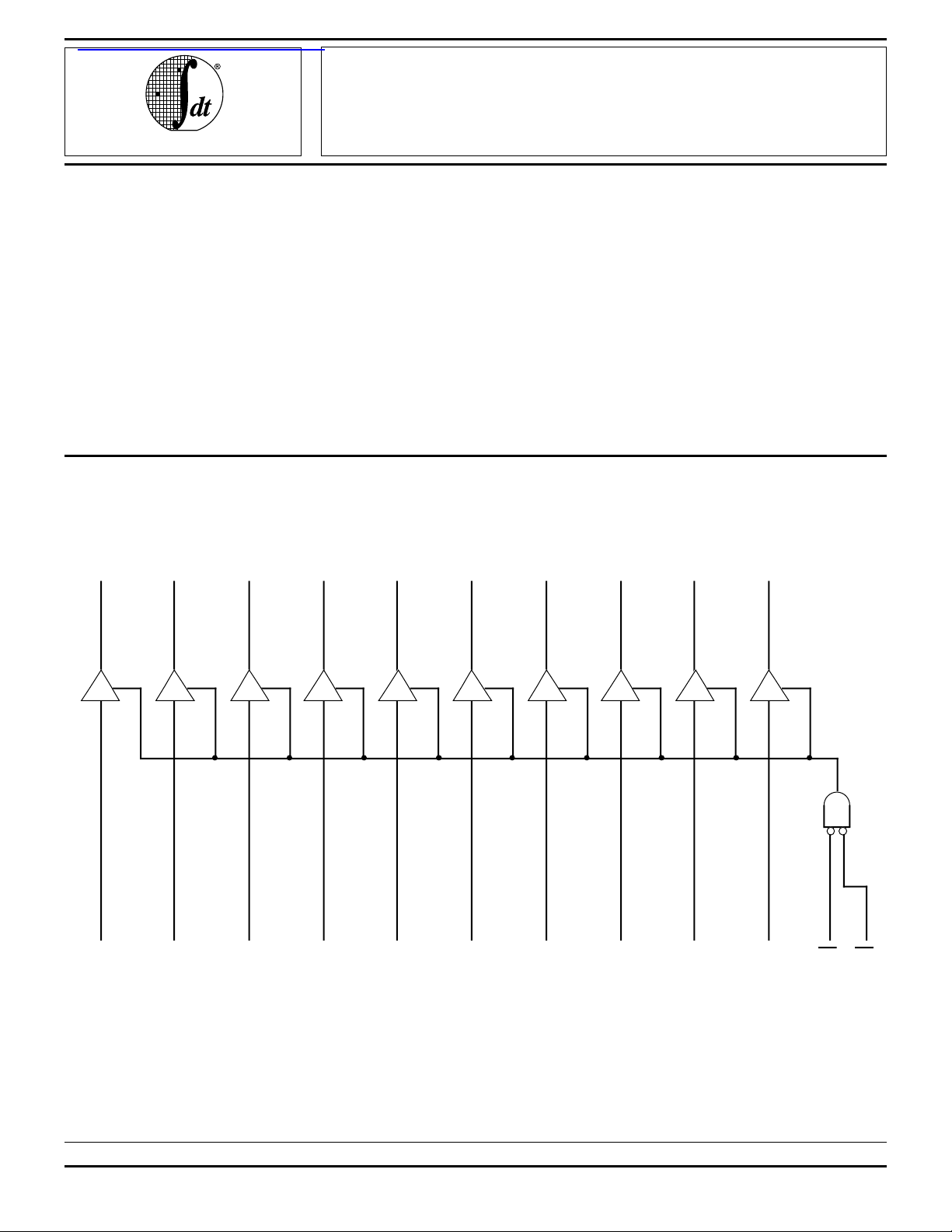
FUNCTIONAL BLOCK DIAGRAM
IDT54/74FCT3827A/B
DESCRIPTION:
The FCT3827A/B 10-bit bus drivers are built using an
advanced dual metal CMOS technology. These high speed,
low power buffers are ideal for high-performance bus interface
buffering for wide data/address paths or buses carrying parity.
The 10-bit buffers have NAND-ed output enables for maximum control flexibility.
All of the FCT3827 high performance interface components are designed for high-capacitance load drive capability,
while providing low-capacitance bus loading at both inputs
and outputs.
Y0 Y1 Y2 Y3 Y4 Y5 Y6 Y7 Y8 Y9
D0 D1 D2 D3 D4 D5 D6 D7 D8 D9 OE1 OE2
3092 drw 01
The IDT logo is a registered trademark of Integrated Device Technology, Inc.
MILITARY AND COMMERCIAL TEMPERATURE RANGES AUGUST 1995
1995 Integrated Device Technology, Inc. 8.15 DSC-4651/-
1
IDT54/74FCT3827A/B
3.3V CMOS OCTAL BUFFERS MILITARY AND COMMERCIAL TEMPERATURE RANGES
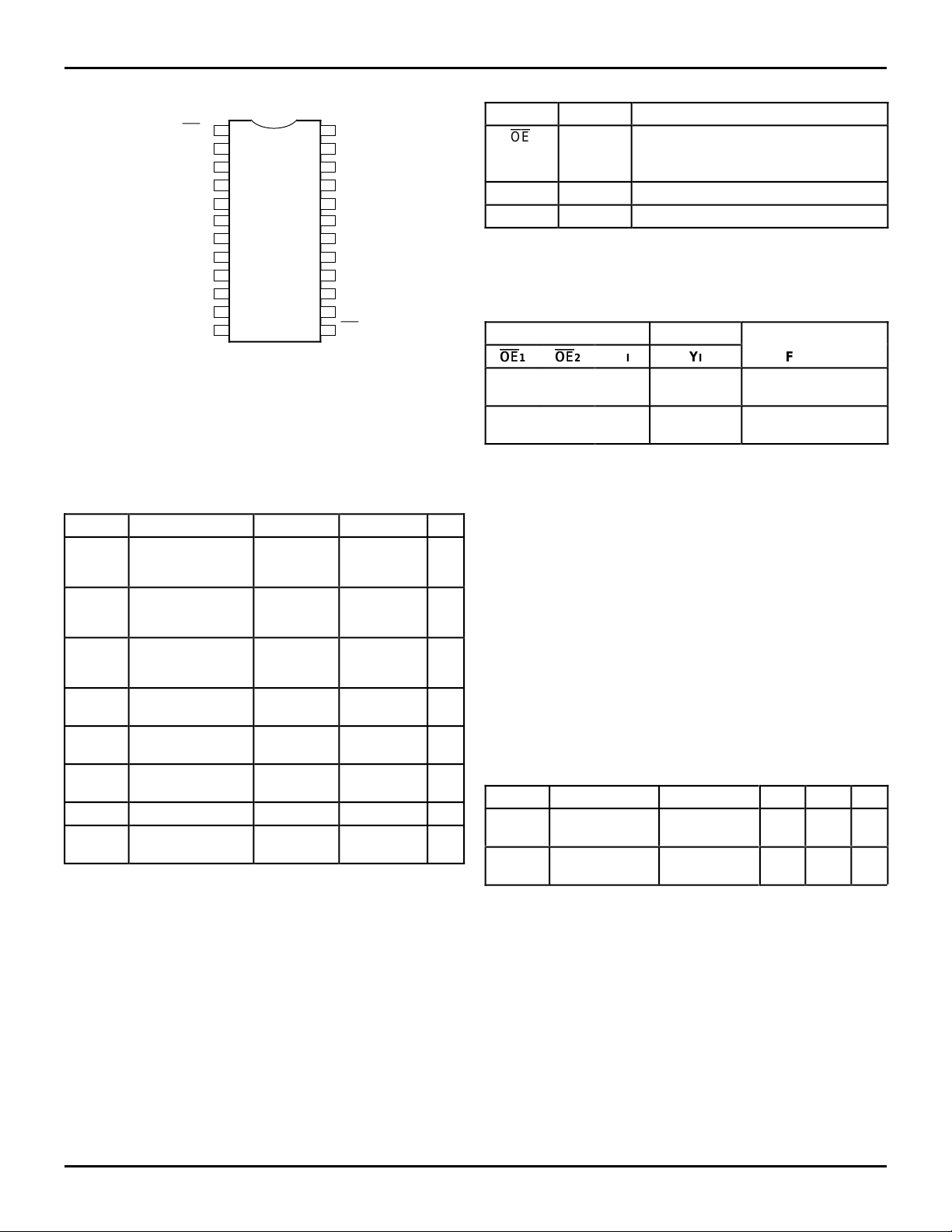
PIN CONFIGURATIONS
VCC1
OE1
2
D0
3
D1
4
D2
D3
D4
D5
D6
D7
D
D9
8
5
6
SO24-2
7
SO24-7
8
SO24-8
9
10
11
P24-1
D24-1
12
DIP/SOIC/SSOP/QSOP
TOP VIEW
ABSOLUTE MAXIMUM RATINGS
Symbol Rating Commercial Military Unit
(2)
VTERM
VTERM
VTERM
TA Operating
TBIAS Temperature
TSTG Storage
PT Power Dissipation 1.0 1.0 W
IOUT DC Output
NOTES:
1. Stresses greater than those listed under ABSOLUTE MAXIMUM RATINGS may cause permanent damage to the device. This is a stress rating
only and functional operation of the device at these or any other conditions
above those indicated in the operational sections of this specification is
not implied. Exposure to absolute maximum rating conditions for extended periods may affect reliability.
2. Vcc terminals.
3. Input terminals.
4. Output and I/O terminals.
Terminal Voltage
with Respect to
GND
(3)
Terminal Voltage
with Respect to
GND
(4)
Terminal Voltage
with Respect to
GND
Temperature
Under Bias
Temperature
Current
24
23
Y0
22
Y1
21
Y2
20
Y3
19
Y4
18
Y5
17
&
16
15
14
13
Y6
Y7
Y8
Y9
OE2GND
3092 drw 02
(1)
–0.5 to +4.6 –0.5 to +4.6 V
–0.5 to +7.0 –0.5 to +7.0 V
–0.5 to
CC + 0.5
V
–0.5 to
VCC + 0.5
V
–40 to +85 –55 to +125 °C
–55 to +125 –65 to +135 °C
–55 to +125 –65 to +150 °C
–60 to +60 –60 to +60 mA
3092 lnk 03
PIN DESCRIPTION
Names I/O Description
OE
I I When both are LOW the outputs are
enabled. When either one or both are
HIGH the outputs are High Z.
DI I 10-bit data input.
YI O 10-bit data output.
FUNCTION TABLE
(1)
Inputs Output
OE
1
OE
OE
L
L
H
X
NOTE:
1. H = HIGH Voltage Level
X = Don’t Care
L = LOW Voltage Level
Z = High Impedance
2 DI YI Function
OE
L
L
X
H
L
H
X
X
L
Transparent
H
Z
Three-State
Z
CAPACITANCE (TA = +25°C, f = 1.0MHz)
Symbol Parameter
CIN Input
Capacitance
COUT Output
Capacitance
NOTE:
1. This parameter is measured at characterization but not tested.
(1)
Conditions Typ. Max. Unit
VIN = 0V 3.5 6.0 pF
VOUT = 0V 4.0 8.0 pF
3092 tbl 01
3092 tbl 02
3092 lnk 04
8.15 2
IDT54/74FCT3827A/B
3.3V CMOS OCTAL BUFFERS MILITARY AND COMMERCIAL TEMPERATURE RANGES
DC ELECTRICAL CHARACTERISTICS OVER OPERATING RANGE
Following Conditions Apply Unless Otherwise Specified:
Commercial: TA = –40°C to +85°C, VCC = 2.7V to 3.6V; Military: TA = –55°C to +125°C, VCC = 2.7V to 3.6V
Symbol Parameter Test Conditions
(1)
Min. Typ.
VIH Input HIGH Level (Input pins) Guaranteed Logic HIGH Level 2.0 — 5.5 V
Input HIGH Level (I/O pins) 2.0 — VCC+0.5
VIL Input LOW Level Guaranteed Logic LOW Level –0.5 — 0.8 V
(Input and I/O pins)
(6)
(6)
(6)
VCC = Max. VI = 5.5V — — ±1 µA
VI = VCC — — ±1
(6)
VI = GND — — ±1
VI = GND — — ±1
II H Input HIGH Current (Input pins)
Input HIGH Current (I/O pins)
II L Input LOW Current (Input pins)
Input LOW Current (I/O pins)
IOZH High Impedance Output Current VCC = Max. VO = VCC — — ±1 µA
IOZL (3-State Output pins)
(6)
VO = GND — — ±1
VIK Clamp Diode Voltage VCC = Min., IIN = –18mA — –0.7 –1.2 V
IODH Output HIGH Current VCC = 3.3V, VIN = VIH or VIL, VO = 1.5V
IODL Output LOW Current VCC = 3.3V, VIN = VIH or VIL, VO = 1.5V
(3)
(3)
–36 –60 –110 mA
50 90 200 mA
VOH Output HIGH Voltage VCC = Min. IOH = –0.1mA VCC–0.2 — — V
VIN = VIH or VIL IOH = –3mA 2.4 3.0 —
(5)
VCC = 3.0V
IN = VIH or VIL
V
IOH = –6mA MIL.
OH = –8mA COM'L.
I
2.4
VOL Output LOW Voltage VCC = Min. IOL = 0.1mA — — 0.2 V
VIN = VIH or VIL IOL = 16mA — 0.2 0.4
IOL = 24mA — 0.3 0.55
IOS Short Circuit Current
(4)
VCC = 3.0V
IN = VIH or VIL
V
VCC = Max., VO = GND
IOL = 24mA — 0.3 0.50
(3)
–60 –135 –240 mA
VH Input Hysteresis — — 150 — mV
ICCL
ICCH
Quiescent Power Supply Current VCC = Max.,
IN = GND or VCC
V
COM'L. — 0.1 10 µA
ICCZ MIL. — 0.1 100
NOTES:
1. For conditions shown as Max. or Min., use appropriate value specified under Electrical Characteristics for the applicable device type.
2. Typical values are at Vcc = 3.3V, +25°C ambient.
3. Not more than one output should be tested at one time. Duration of the test should not exceed one second.
4. This parameter is guaranteed but not tested.
5. V
OH = VCC –0.6V at rated current.
6. The test limits for this parameter is ± 5µA at T
A = –55°C.
(2)
Max. Unit
3.0 —
3092 lnk 05
8.15 3
 Loading...