


Integrated Device Technology, Inc.
FAST CMOS OCTAL D
REGISTERS (3-STATE)
IDT54/74FCT374T/AT/CT/DT - 2374T/AT/CT
IDT54/74FCT534T/AT/CT
IDT54/74FCT574T/AT/CT/DT - 2574T/AT/CT
FEATURES:
• Common features:
– Low input and output leakage ≤1µA (max.)
– CMOS power levels
– True TTL input and output compatibility
– VOH = 3.3V (typ.)
– V
OL = 0.3V (typ.)
– Meets or exceeds JEDEC standard 18 specifications
– Product available in Radiation Tolerant and Radiation
Enhanced versions
– Military product compliant to MIL-STD-883, Class B
and DESC listed (dual marked)
– Available in DIP, SOIC, SSOP, QSOP, CERPACK
and LCC packages
• Features for FCT374T/FCT534T/FCT574T:
– Std., A, C and D speed grades
DESCRIPTION
The FCT374T/FCT2374T, FCT534T and FCT574T/
FCT2574T are 8-bit registers built using an advanced dual
metal CMOS technology. These registers consist of eight Dtype flip-flops with a buffered common clock and buffered 3state output control. When the output enable (OE) input is
LOW, the eight outputs are enabled. When the OE input is
HIGH, the outputs are in the high-impedance state.
Input data meeting the set-up and hold time requirements
of the D inputs is transferred to the Q outputs on the LOW-toHIGH transition of the clock input.
The FCT2374T and FCT2574T have balanced output drive
with current limiting resistors. This offers low ground bounce,
minimal undershoot and controlled output fall times-reducing
the need for external series terminating resistors. FCT2xxxT
parts are plug-in replacements for FCTxxxT parts.
– High drive outputs (-15mA IOH, 48mA IOL)
• Features for FCT2374T/FCT2574T:
– Std., A, and C speed grades
– Resistor outputs (-15mA IOH, 12mA IOL Com.)
(-12mA IOH, 12mA IOL Mil.)
– Reduced system switching noise
FUNCTIONAL BLOCK DIAGRAM FCT374/FCT2374T AND FCT574/FCT2574T
D0
D1
D2
D3
D4
D5
D6
D7
CP
OE
CP
D
Q
Q0
D
CP
QQQ Q
Q1
CP
FUNCTIONAL BLOCK DIAGRAM FCT534T
D0
CP
D
CP
Q
OE
Q0
The IDT logo is a registered trademark of Integrated Device Technology, Inc.
CP
D1
D
Q
Q1
CP
D
Q2
D2
D
Q
Q2
CP
CP
D
Q3
D3
D
Q
Q3
CP
CP
D
Q4
D4
D
Q
Q4
D
CP
Q
Q5
D5
D
CP
Q
Q5
D
CP
QQ
Q6
D6
D
CP
Q
Q6
D
CP
Q7
2569 drw 01
D7
D
CP
Q
Q7
2569 drw 02
MILITARY AND COMMERCIAL TEMPERATURE RANGES AUGUST 1995
1995 Integrated Device Technology, Inc. 6.13 DSC-4214/5
1

IDT54/74FCT374T/AT/CT/DT - 2374T/AT/CT, IDT54/74FCT534T/AT/CT, IDT54/74FCT574T/AT/CT/DT - 2574T/AT/CT
FAST CMOS OCTAL D REGISTERS (3-STATE) MILITARY AND COMMERCIAL TEMPERATURE RANGES
PIN CONFIGURATIONS
IDT54/74FCT374T
OE
Q
D0
D1
Q1
Q2
D2
D3
Q3
GND
DIP/SOIC/SSOP/QSOP/CERPACK
IDT54/74FCT574T
OE
D
D
D
D
D
D
D
D
GND
DIP/SOIC/SSOP/QSOP/CERPACK
0
2
3
4
5
6
7
8
9
10 11
1
2
0
3
1
2
4
3
5
4
6
5
7
6
8
9
7
10 11
P20-1
D20-1
SO20-2
SO20-7
SO20-8
&
E20-1
TOP VIEW
P20-1
D20-1
SO20-2
SO20-7
SO20-8
&
E20-1
TOP VIEW
20
19
18
17
16
15
14
13
12
20
19
18
17
16
15
14
13
12
VCC1
Q
D7
D6
Q6
Q5
D
D4
Q4
CP
V
Q
Q
Q
Q
Q
Q
Q
Q
CP
5
CC
0
1
2
3
4
5
6
7
INDEX
7
D
1
Q
1
Q
2
D
2
D
3
0Q0
D
OE
3 2 20 19
4
1
5
6
L20-2
7
8
CCQ7
V
18
17
16
15
14
D
7
D
6
Q
6
Q
5
D
5
910111213
GND
CP
4
4
Q
D
2569 drw 03
3
Q
LCC
TOP VIEW
INDEX
D2
D3
D4
D5
D6
D1
3 2 20 19
4
5
6
7
8
D0
1
L20-2
OE
CC
V
Q0
18
17
16
15
14
Q1
Q2
Q3
Q4
Q5
9 10111213
GND
CP
7
Q
Q6
2569 drw 04
D7
LCC
TOP VIEW
IDT54/74FCT534T
OE
Q
D0
D1
Q1
Q2
D2
D3
Q3
GND
20
2
0
3
P20-1
4
D20-1
5
SO20-2
6
SO20-8
7
E20-1
8
9
19
18
17
16
15
&
14
13
12
10 11
DIP/SOIC/QSOP/CERPACK
TOP VIEW
VCC1
Q
D7
D6
Q6
Q5
D
D4
Q4
CP
INDEX
7
D1 D7
Q1
Q2
D2
D3
5
D0
Q0
OE
3 2 20 19
4
1
5
6
L20-2
7
8
9 10111213
Q3
GND
CP
VCC
4
Q
Q7
D4
18
17
16
15
14
D
Q6
Q5
D5
6
2569 drw 05
LCC
TOP VIEW
6.13 2
IDT54/74FCT374T/AT/CT/DT - 2374T/AT/CT, IDT54/74FCT534T/AT/CT, IDT54/74FCT574T/AT/CT/DT - 2574T/AT/CT
FAST CMOS OCTAL D REGISTERS (3-STATE) MILITARY AND COMMERCIAL TEMPERATURE RANGES
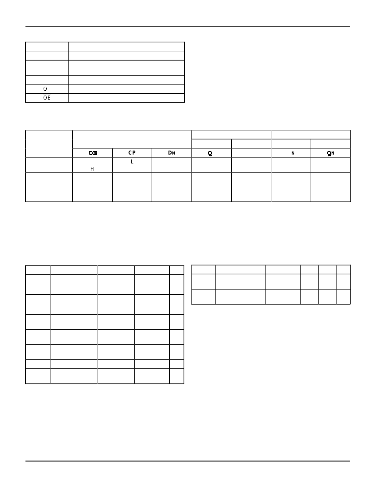
PIN DESCRIPTION
Pin Names Description
DN D flip-flop data inputs
CP Clock Pulse for the register. Enters data on
LOW-to-HIGH transition.
QN 3-state outputs, (true)
Q
N 3-state outputs, (inverted)
OE
Active LOW 3-state Output Enable input
2569 tbl 01
FUNCTION TABLE
(1)
534 374/574
Inputs Outputs Internal Outputs Internal
Function
HI-Z H
LOAD REGISTER L
NOTE: 2569 tbl 02
1. H = HIGH Voltage Level
L = LOW Voltage Level
X = Don’t Care
Z = High Impedance
NC = No Change
OE
OE
H
L
H
H
CP DN
L
H
X
X
↑
↑
H
↑
↑
H
Q
N QN QN
Q
Z
Z
L
H
L
L
Z
Z
NC
NC
L
H
L
H
Z
Z
L
H
Z
Z
Q
Q
NC
NC
H
L
H
L
N
↑ = LOW-to-HIGH transition
ABSOLUTE MAXIMUM RATINGS
Symbol Rating Commercial Military Unit
(2)
VTERM
VTERM
TA Operating
TBIAS Temperature
TSTG Storage
PT Power Dissipation 0.5 0.5 W
IOUT DC Output
NOTES:
1. Stresses greater than those listed under ABSOLUTE MAXIMUM RATINGS may cause permanent damage to the device. This is a stress rating
only and functional operation of the device at these or any other conditions
above those indicated in the operational sections of this specification is
not implied. Exposure to absolute maximum rating conditions for
extended periods may affect reliability. No terminal voltage may exceed
V
2. Input and V
3. Outputs and I/O terminals only.
Terminal Voltage
–0.5 to +7.0 –0.5 to +7.0 V
with Respect to
GND
(3)
Terminal Voltage
with Respect to
GND
–0.5 to
V
0 to +70 –55 to +125 °C
Temperature
–55 to +125 –65 to +135 °C
Under Bias
–55 to +125 –65 to +150 °C
Temperature
–60 to +120 –60 to +120 mA
Current
CC by +0.5V unless otherwise noted.
CC terminals only.
CC +0.5
(1)
–0.5 to
VCC +0.5
V
2569 lnk 03
CAPACITANCE (TA = +25°C, f = 1.0MHz)
Symbol Parameter
CIN Input
Capacitance
COUT Output
Capacitance
NOTE:
1. This parameter is measured at characterization but not tested.
(1)
Conditions Typ. Max. Unit
VIN = 0V 6 10 pF
VOUT = 0V 8 12 pF
2569 lnk 04
6.13 3
 Loading...