

IDT IDT54FCT16244T, IDT54FCT16244AT, IDT54FCT16244CT, IDT54FCT16244ET, IDT54FCT162244T User Manual
...
Integrated Device Technology, Inc.
FAST CMOS 16-BIT
BUFFER/LINE DRIVER
IDT54/74FCT16244T/AT/CT/ET
IDT54/74FCT162244T/AT/CT/ET
IDT54/74FCT166244T/AT/CT
IDT54/74FCT162H244T/AT/CT/ET
FEATURES:
• Common features:
– 0.5 MICRON CMOS Technology
– High-speed, low-power CMOS replacement for
ABT functions
– Typical tSK(o) (Output Skew) < 250ps
– Low input and output leakage ≤ 1µA (max.)
– ESD > 2000V per MIL-STD-883, Method 3015;
> 200V using machine model (C = 200pF, R = 0)
– Packages include 25 mil pitch SSOP, 19.6 mil pitch
TSSOP, 15.7 mil pitch TVSOP and 25 mil pitch Cerpack
– Extended commercial range of -40°C to +85°C
• Features for FCT16244T/AT/CT/ET:
– High drive outputs (-32mA I
OH, 64mA IOL)
– Power off disable outputs permit “live insertion”
– Typical VOLP (Output Ground Bounce) < 1.0V at
VCC = 5V, TA = 25°C
• Features for FCT162244T/AT/CT/ET:
– Balanced Output Drivers: ±24mA (commercial),
±16mA (military)
– Reduced system switching noise
– Typical VOLP (Output Ground Bounce) < 0.6V at
VCC = 5V,TA = 25°C
• Features for FCT166244T/AT/CT:
– Light Drive Balanced Output: ±8mA (commercial),
±6mA (military)
– Minimal system switching noise
– Typical VOLP (Output Ground Bounce) < 0.25V at
V
CC = 5V,TA = 25°C
• Features for FCT162H244T/AT/CT/ET:
– Bus-Hold retains last active bus state during 3-state
– Eliminates the need for external pull up resistors
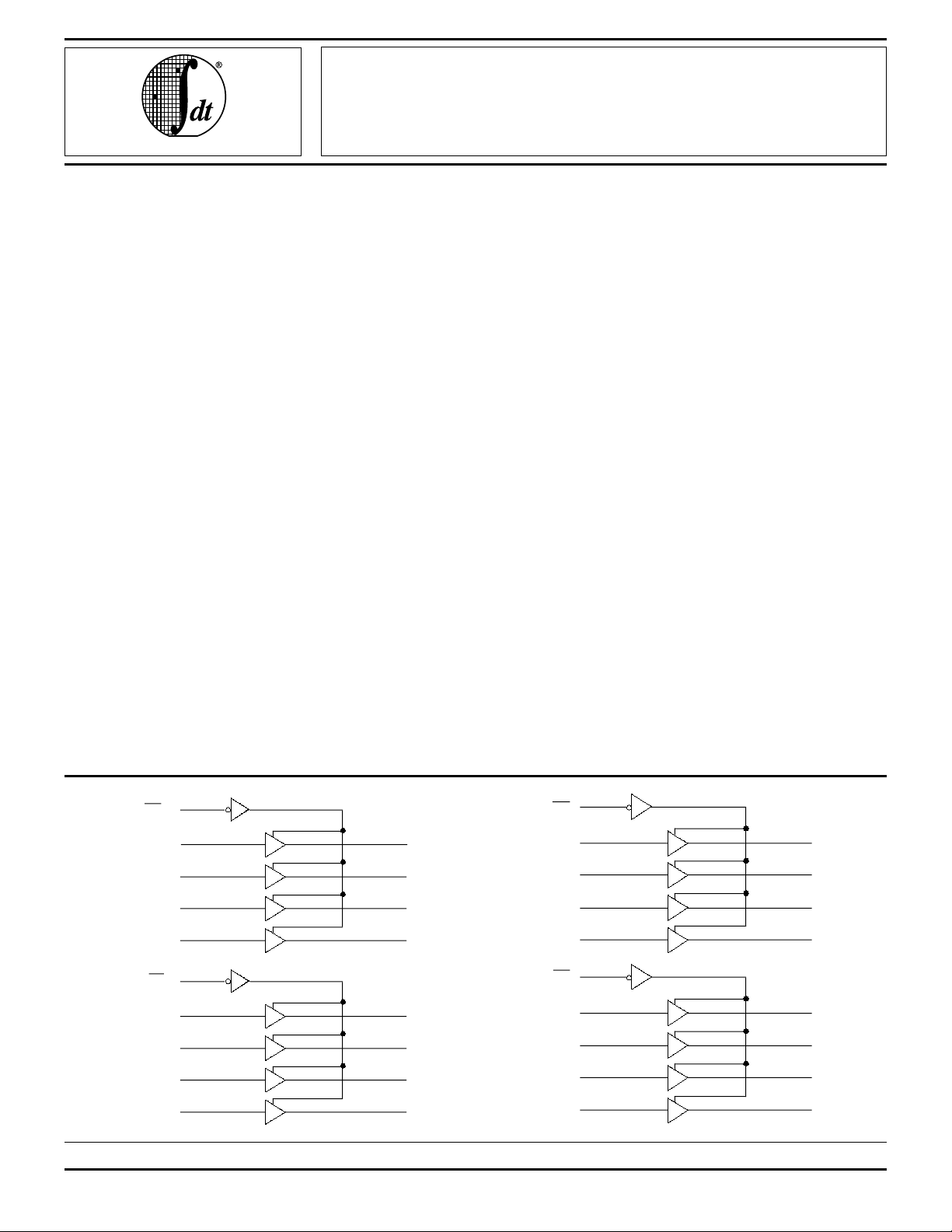
FUNCTIONAL BLOCK DIAGRAM
1OE
DESCRIPTION:
The 16-Bit Buffer/Line Driver is for bus interface or signal buffering
applications requiring high speed and low power dissipation. These
devices have a flow through pin organization, and shrink packaging
to simplify board layout. All inputs are designed with hysteresis for
improved noise margin. The three-state controls allow independent
4-bit, 8-bit or combined 16-bit operation. These parts are plug in
replacements for 54/74ABT16244 where higher speed, lower noise
or lower power dissipation levels are desired.
The FCT16244T/AT/CT/ET are ideally suited for driving
high capacitance loads (>200pF) and low impedance
backplanes. These "high drive" buffers are designed with
power off disable capability to allow "live insertion" of boards
when used in a backplane interface.
The FCT162244T/AT/CT/ET have balanced output current
levels and current limiting resistors. These offer low ground
bounce, minimal undershoot, and controlled output fall times,
reducing the need for external series terminating resistors
while still providing very high speed operation for loads of less
than 200pF.
The FCT166244T/AT/CT are suited for very low noise,
point-to-point driving where there is a single receiver, or a very
light lumped load (<100pF). The buffers are designed to limit
the output current to levels which will avoid noise and ringing
on the signal lines without using external series terminating
resistors.
The FCT162H244T/AT/CT/ET have "Bus-Hold" which retains the input's last state whenever the input goes to high
impedance. This prevents "floating" inputs and eliminates the
need for pull-up/down resistors.
3OE
A1
1
1A2
1
A3
A4
1
2OE
2A1
2A2
2
A3
A4
2
The IDT logo is a registered trademark of Integrated Device Technology, Inc.
1Y1
Y2
1
Y3
1
Y4
1
Y1
2
2
Y2
2
Y3
Y4
2
2544 drw 01
3A1
3
A2
3
A3
A4
3
4OE
4A1
A2
4
A3
4
A4
4
Y1
3
3Y2
3
Y3
Y4
3
4Y1
Y2
4
Y3
4
Y4
4
2544 drw 02
MILITARY AND COMMERCIAL TEMPERATURE RANGES OCTOBER 1996
1996 Integrated Device Technology, Inc. 5.2 DSC-2544/9
15
IDT54/74FCT16244T/AT/CT/ET, 162244T/AT/CT/ET,
166244T/AT/CT, 162H244T/AT/CT/ET FAST CMOS 16-BIT BUFFER/LINE DRIVER MILITARY AND COMMERCIAL TEMPERATURE RANGES
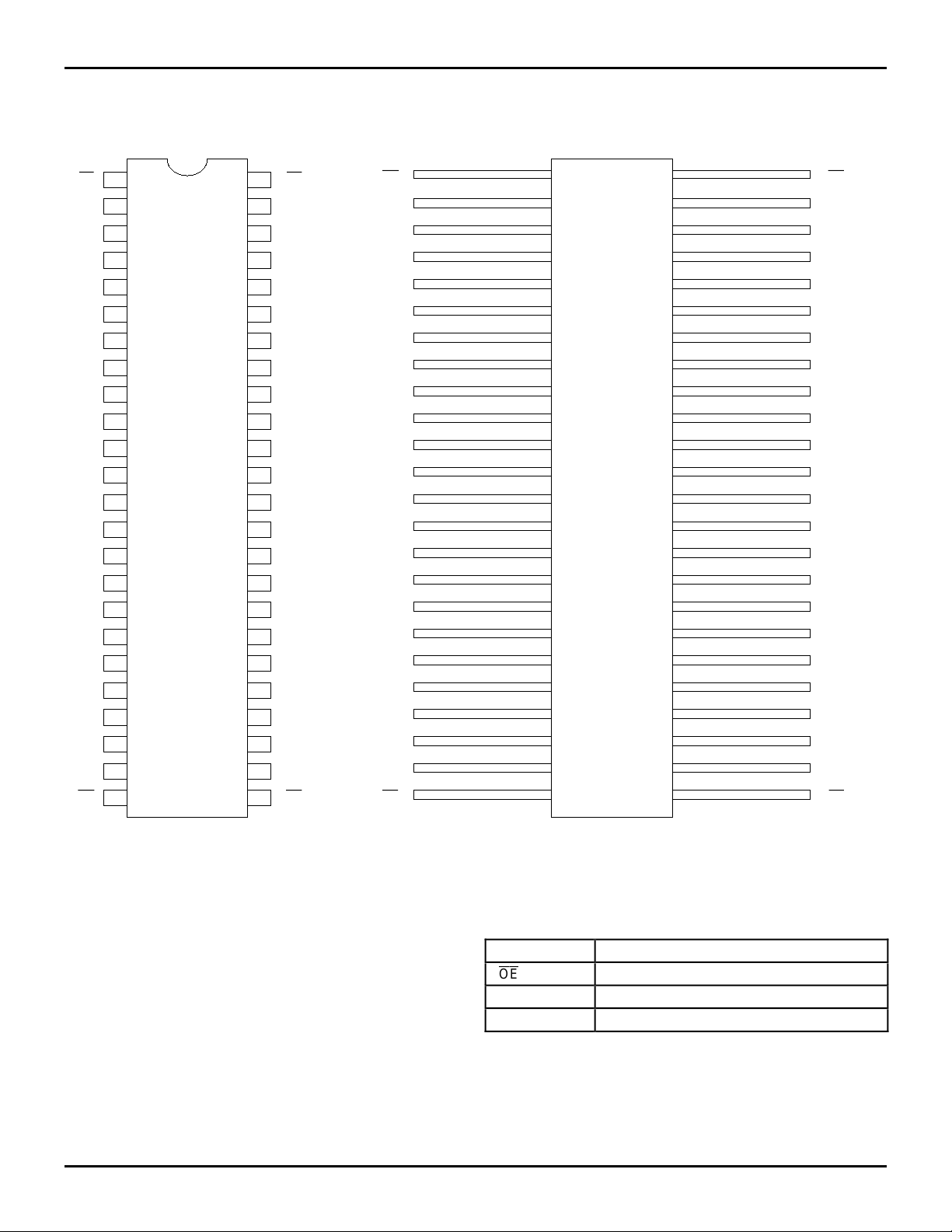
PIN CONFIGURATIONS
1OE
1Y1
1Y2
GND
1Y3
1
Y4
VCC
Y1
2
2
Y2
GND
Y3
2
Y4
2
Y1
3
3Y2
GND
3
Y3
3
Y4
1
2
3
4
5
6
7
8
9
10
11
12
13
14
15
16
17
SO48-1
SO48-2
SO48-3
48
47
46
45
44
43
42
41
40
39
38
37
36
35
34
33
32
2OE
1A1
A2
1
GND
1A3
A4
1
VCC
A1
2
A2
2
GND
A3
2
A4
2
A1
3
A2
3
GND
A3
3
A4
3
OE
1
1Y1
1Y2
GND
1Y3
1
Y4
VCC
2
Y1
2
Y2
GND
2
Y3
2
Y4
3
Y1
3Y2
GND
Y3
3
3
Y4
1
2
3
4
5
6
7
8
9
10
11
12
13
14
15
16
17
E48-1
48
47
46
45
44
43
42
41
40
39
38
37
36
35
34
33
32
2OE
1A1
1
A2
GND
1A3
1
A4
VCC
2
A1
2
A2
GND
2
A3
2
A4
3
A1
A2
3
GND
3
A3
3
A4
V
CC
4
Y1
Y2
4
GND
4
Y3
Y4
4
4OE
18
19
20
21
22
23
24
SSOP/
TSSOP/TVSOP
TOP VIEW
31
30
29
28
27
26
25
VCC
A1
4
A2
4
GND
4
A3
A4
4
3OE
2544 drw 03
CC
V
4
Y1
Y2
4
GND
4
Y3
4
Y4
4OE
18
19
20
21
22
23
24
31
30
29
28
27
26
25
2544 drw 04
VCC
4
A1
A2
4
GND
4
A3
4
A4
3OE
CERPACK
TOP VIEW
PIN DESCRIPTION
Pin Names Description
x
OE
xAx Data Inputs
xYx 3-State Outputs
NOTE:
1. On FCT16xH these pins have “Bus-hold”. All other pins are standard
inputs, outputs or I/Os.
3–State Output Enable Inputs (Active LOW)
(1)
2544 tbl 01
5.2 2
IDT54/74FCT16244T/AT/CT/ET, 162244T/AT/CT/ET,
166244T/AT/CT, 162H244T/AT/CT/ET FAST CMOS 16-BIT BUFFER/LINE DRIVER MILITARY AND COMMERCIAL TEMPERATURE RANGES
ABSOLUTE MAXIMUM RATINGS
(1)
Symbol Description Max. Unit
(2)
VTERM
VTERM
Terminal Voltage with Respect to
GND
(3)
Terminal Voltage with Respect to
GND
–0.5 to +7.0 V
–0.5 to
CC +0.5
V
V
TSTG Storage Temperature –65 to +150 °C
IOUT DC Output Current –60 to +120 mA
NOTES:
1. Stresses greater than those listed under ABSOLUTE MAXIMUM RATINGS
may cause permanent damage to the device. This is a stress rating only
and functional operation of the device at these or any other conditions
above those indicated in the operational sections of this specification is
not implied. Exposure to absolute maximum rating conditions for
extended periods may affect reliability.
2. All device terminals except FCT162XXXT and FCT166XXXT output and
I/O terminals.
3. Output and I/O terminals for FCT162XXXT and FCT166XXXT.
2544 lnk 03
FUNCTION TABLE
(1)
Inputs Outputs
x
OEOE xAx xYx
LLL
LHH
HXZ
NOTE:
1. H = HIGH Voltage Level
X = Don’t Care
L = LOW Voltage Level
Z = High Impedance
CAPACITANCE (TA = +25°C, f = 1.0MHz)
Symbol Parameter
C
IN
Input
Capacitance
C
OUT
Output
Capacitance
NOTE:
1. This parameter is measured at characterization but not tested.
(1)
Conditions Typ. Max. Unit
VIN = 0V 3.5 6.0
V
OUT
= 0V 3.5 8.0
2544 tbl 02
pF
pF
2544 lnk 04
DC ELECTRICAL CHARACTERISTICS OVER OPERATING RANGE (STANDARD PARTS)
Following Conditions Apply Unless Otherwise Specified:
Commercial: TA = –40°C to +85°C, VCC = 5.0V ± 10%; Military: TA = –55°C to +125°C, VCC = 5.0V ± 10%
Symbol Parameter Test Conditions
(1)
Min. Typ.
VIH Input HIGH Level Guaranteed Logic HIGH Level 2.0 — — V
VIL Input LOW Level Guaranteed Logic LOW Level — — 0.8 V
II H Input HIGH Current (Input pins)
Input HIGH Current (I/O pins)
II L Input LOW Current (Input pins)
Input LOW Current (I/O pins)
(5)
VCC = Max. VI = VCC — — ±1 µA
(5)
(5)
VI = GND — — ±1
(5)
— — ±1
— — ±1
IOZH High Impedance Output Current VCC = Max. VO = 2.7V — — ±1 µA
IOZL (3-State Output pins)
(5)
VO = 0.5V — — ±1
VIK Clamp Diode Voltage VCC = Min., IIN = –18mA — –0.7 –1.2 V
IOS Short Circuit Current VCC = Max., VO = GND
(3)
–80 –140 –225 mA
VH Input Hysteresis — — 100 — mV
ICCL
Quiescent Power Supply Current VCC = Max., VIN = GND or VCC — 5 500 µA
ICCH
ICCZ
NOTES:
1. For conditions shown as Max. or Min., use appropriate value specified under Electrical Characteristics for the applicable device type.
2. Typical values are at Vcc = 5.0V, +25°C ambient.
3. Not more than one output should be tested at one time. Duration of the test should not exceed one second.
4. Duration of the condition can not exceed one second.
5. The test limit for this parameter is ± 5µA at T
A = –55°C.
(2)
Max. Unit
2544 lnk 05
5.2 3

IDT54/74FCT16244T/AT/CT/ET, 162244T/AT/CT/ET,
166244T/AT/CT, 162H244T/AT/CT/ET FAST CMOS 16-BIT BUFFER/LINE DRIVER MILITARY AND COMMERCIAL TEMPERATURE RANGES
DC ELECTRICAL CHARACTERISTICS OVER OPERATING RANGE (BUS-HOLD)
Following Conditions Apply Unless Otherwise Specified:
Commercial: TA = –40°C to +85°C, VCC = 5.0V ± 10%; Military: TA = –55°C to +125°C, VCC = 5.0V ± 10%
Symbol Parameter Test Conditions
(1)
Min. Typ.
VIH Input HIGH Level Guaranteed Logic HIGH Level 2.0 — — V
VIL Input LOW Level Guaranteed Logic LOW Level — — 0.8 V
(5)
(5)
VCC = Max. VI = VCC ——±1µA
——±1
II H Input Standard Input
HIGH Standard I/O
(4)
Current
Bus-hold Input — — ±100
Bus-hold I/O — — ±100
II L Input Standard Input
LOW Standard I/O
(4)
Current
Bus-hold Input — — ±100
(5)
(5)
——±1
VI = GND — — ±1
Bus-hold I/O — — ±100
IBHH Bus Hold Bus-hold Input VCC = Min. VI = 2.0V –50 — — µA
IBHL Sustain
Current
(4)
V
I = 0.8V +50 — —
IOZH High Impedance Output Current VCC = Max. VO = 2.7V — — ±1 µA
IOZL (3-State Output pins)
(5,6)
VO = 0.5V — — ±1
VIK Clamp Diode Voltage VCC = Min., IIN = –18mA — –0.7 –1.2 V
IOS Short Circuit Current VCC = Max., VO = GND
(3)
–80 –140 –225 mA
VH Input Hysteresis — — 100 — mV
ICCL
Quiescent Power Supply Current VCC = Max., VIN = GND or VCC — 5 500 µA
ICCH
ICCZ
NOTES:
1. For conditions shown as Max. or Min., use appropriate value specified under Electrical Characteristics for the applicable device type.
2. Typical values are at Vcc = 5.0V, +25°C ambient.
3. Not more than one output should be tested at one time. Duration of the test should not exceed one second.
4. Pins with Bus-hold are identified in the pin description.
5. The test limit for this parameter is ± 5µA at T
6. Does not include Bus-hold I/O pins.
A = –55°C.
(2)
Max. Unit
2544 lnk 06
5.2 4

IDT54/74FCT16244T/AT/CT/ET, 162244T/AT/CT/ET,
166244T/AT/CT, 162H244T/AT/CT/ET FAST CMOS 16-BIT BUFFER/LINE DRIVER MILITARY AND COMMERCIAL TEMPERATURE RANGES
OUTPUT DRIVE CHARACTERISTICS FOR FCT16244T
Symbol Parameter Test Conditions
IO Output Drive Current VCC = Max., VO = 2.5V
(3)
(1)
Min. Typ.
–50 —–180 mA
VOH Output HIGH Voltage VCC = Min. IOH = –3mA 2.5 3.5 — V
VIN = VIH or VIL IOH = –12mA MIL.
VOL Output LOW Voltage VCC = Min.
IN = VIH or VIL
V
IOFF Input/Output Power Off Leakage
(5)
VCC = 0V, VIN or VO ≤ 4.5V — — ±1 µA
OH = –15mA COM'L.
I
IOH = –24mA MIL.
OH = –32mA COM'L.
I
IOL = 48mA MIL.
OL = 64mA COM'L.
I
2.4 3.5 — V
2.0 3.0 — V
(4)
— 0.2 0.55 V
(2)
Max. Unit
2544 lnk 07
OUTPUT DRIVE CHARACTERISTICS FOR FCT162244T
Symbol Parameter Test Conditions
(1)
IODL Output LOW Current VCC = 5V, VIN = VIH or VIL, VOUT = 1.5V
IODH Output HIGH Current VCC = 5V, VIN = VIH or V IL,
VOH Output HIGH Voltage VCC = Min.
V
IN = VIH or VIL
VOL Output LOW Voltage VCC = Min.
V
IN = VIH or VIL
VOUT = 1.5V
IOH = –16mA MIL.
I
OH = –24mA COM'L.
IOL = 16mA MIL.
I
OL = 24mA COM'L.
(3)
(3)
Min. Typ.
60 115 200 mA
–60 –115 –200 mA
2.4 3.3 — V
— 0.3 0.55 V
(2)
Max. Unit
2544 lnk 08
OUPUT DRIVE CHARACTERISTICS FOR FCT166244T
Symbol Parameter Test Conditions
I
ODL
I
ODH
V
OH
V
OL
NOTES:
1. For conditions shown as Max. or Min., use appropriate value specified under Electrical Characteristics for the applicable device type.
2. Typical values are at Vcc = 5.0V, +25°C ambient.
3. Not more than one output should be tested at one time. Duration of the test should not exceed one second.
4. Duration of the condition can not exceed one second.
5. The test limit for this parameter is ± 5µA at T
Output LOW Current VCC = 5V, V
Output HIGH Current VCC = 5V, V
Output HIGH Voltage VCC = Min.
IN
= V
IH
V
or V
Output LOW Voltage VCC = Min.
IN
= V
IH
V
A = –55°C.
or V
IN
= V
IH or VIL, VOUT
IN
= V
IH
IL
IL
or V
IL,VOUT
(1)
(3)
= 1.5V
(3)
= 1.5V
IOH = –6mA MIL.
OH
= –8mA COM'L.
I
IOL = 6mA MIL.
OL
= 8mA COM'L.
I
Min. Typ.
16 48 96 mA
–16 –48 –96 mA
2.4 3.3 — V
— 0.3 0.55 V
(2)
Max. Unit
2544 lnk 09
5.2 5

IDT54/74FCT16244T/AT/CT/ET, 162244T/AT/CT/ET,
166244T/AT/CT, 162H244T/AT/CT/ET FAST CMOS 16-BIT BUFFER/LINE DRIVER MILITARY AND COMMERCIAL TEMPERATURE RANGES
POWER SUPPLY CHARACTERISTICS
V
IN
= VCC
V
IN
= GND
(1)
Min. Typ.
— 0.5 1.5 mA
— 60 100
Symbol Parameter Test Conditions
∆I
I
CCD
CC
Quiescent Power Supply Current
TTL Inputs HIGH
Dynamic Power Supply
(4)
Current
VCC = Max.
= 3.4V
(3)
V
IN
VCC = Max.
Outputs Open
xOE = GND
One Input Toggling
50% Duty Cycle
I
C
Total Power Supply Current
(6)
VCC = Max.
Outputs Open
V
IN
= VCC
V
IN
= GND
— 0.6 1.5 mA
fi = 10MHz
50% Duty Cycle
x
OE
= GND
V
IN
V
IN
= 3.4V
= GND
— 0.9 2.3
One Bit Toggling
VCC = Max.
Outputs Open
V
IN
= VCC
V
IN
= GND
— 2.4 4.5
fi = 2.5MHz
50% Duty Cycle
xOE = GND
V
IN
V
IN
= 3.4V
= GND
— 6.4 16.5
Sixteen Bits Toggling
NOTES:
1. For conditions shown as Max. or Min., use appropriate value specified under Electrical Characteristics for the applicable device type.
2. Typical values are at V
3. Per TTL driven input (V
4. This parameter is not directly testable, but is derived for use in Total Power Supply Calculations.
5. Values for these conditions are examples of the I
C = IQUIESCENT + IINPUTS + IDYNAMIC
6. I
IC = ICC + ∆ICC DHNT + ICCD (fCPNCP/2 + fiNi)
CC = Quiescent Current (ICCL, ICCH and ICCZ)
I
CC = Power Supply Current for a TTL High Input (VIN = 3.4V)
∆I
H = Duty Cycle for TTL Inputs High
D
T = Number of TTL Inputs at DH
N
ICCD = Dynamic Current Caused by an Input Transition Pair (HLH or LHL)
f
CP = Clock Frequency for Register Devices (Zero for Non-Register Devices)
CP = Number of Clock Inputs at fCP
N
fi = Input Frequency
i = Number of Inputs at fi
N
CC = 5.0V, +25°C ambient.
IN = 3.4V). All other inputs at VCC or GND.
CC formula. These limits are guaranteed but not tested.
(2)
Max. Unit
(5)
(5)
µ
A/
MHz
2544 tbl 10
5.2 6

IDT54/74FCT16244T/AT/CT/ET, 162244T/AT/CT/ET,
166244T/AT/CT, 162H244T/AT/CT/ET FAST CMOS 16-BIT BUFFER/LINE DRIVER MILITARY AND COMMERCIAL TEMPERATURE RANGES
SWITCHING CHARACTERISTICS OVER OPERATING RANGE FOR FCT16244T/FCT162244T
FCT16244T/162244T/166244T FCT16244AT/162244AT/166244AT
Com'l. Mil. Com'l. Mil.
Symbol Parameter Condition
tPLH
tPHL
tPZH
Propagation Delay
xAx to xYx
CL = 50pF
R
Output Enable Time 1.5 8.0 1.5 8.5 1.5 6.2 1.5 6.5 ns
(1)
L = 500Ω
tPZL
tPHZ
Output Disable Time 1.5 7.0 1.5 7.5 1.5 5.6 1.5 5.9 ns
tPLZ
tSK(o) Output Skew
Symbol Parameter Condition
tPLH
tPHL
tPZH
Propagation Delay
xAx to xYx
Output Enable Time 1.5 5.8 1.5 6.5 1.5 4.4 — — ns
(3)
CL = 50pF
L = 500Ω
R
(1)
tPZL
tPHZ
Output Disable Time 1.5 5.2 1.5 5.7 1.5 3.6 — — ns
tPLZ
tSK(o) Output Skew
NOTES:
1. See test circuit and waveforms.
2. Minimum limits are guaranteed but not tested on Propagation Delays.
3. Skew between any two outputs of the same package switching in the same direction. This parameter is guaranteed by design.
(3)
Min.
(2)
Max. Min.
(2)
Max. Min.
(2)
Max. Min.
(2)
Max. Unit
1.5 6.5 1.5 7.0 1.5 4.8 1.5 5.1 ns
— 0.5 — 0.5 — 0.5 — 0.5 ns
2544 tbl 11
FCT16244CT/162244CT/166244CT FCT16244ET/162244ET
Com'l. Mil. Com'l. Mil.
Min.
(2)
Max. Min.
(2)
Max. Min.
(2)
Max. Min.
(2)
Max. Unit
1.5 4.1 1.5 4.6 1.5 3.2 — — ns
— 0.5 — 0.5 — 0.5 — — ns
2544 tbl 12
5.2 7

IDT54/74FCT16244T/AT/CT/ET, 162244T/AT/CT/ET,
166244T/AT/CT, 162H244T/AT/CT/ET FAST CMOS 16-BIT BUFFER/LINE DRIVER MILITARY AND COMMERCIAL TEMPERATURE RANGES
TEST CIRCUITS AND WAVEFORMS
TEST CIRCUITS FOR ALL OUTPUTS
V
CC
7.0V
SWITCH POSITION
Test Switch
Open Drain
Pulse
Generator
500Ω
V
V
IN
OUT
D.U.T.
50pF
T
R
C L
500Ω
2544 drw 05
DEFINITIONS:
C
L= Load capacitance: includes jig and probe capacitance.
T = Termination resistance: should be equal to ZOUT of the Pulse
R
Disable Low
Enable Low
All Other Tests
Generator.
SET-UP, HOLD AND RELEASE TIMES PULSE WIDTH
DATA
INPUT
TIMING
INPUT
ASYNCHRONOUS CONTROL
PRESET
CLEAR
ETC.
SYNCHRONOUS CONTROL
PRESET
CLEAR
CLOCK ENABLE
ETC.
tSU
tSU
tH
tREM
tH
3V
1.5V
0V
3V
1.5V
0V
3V
1.5V
0V
3V
1.5V
0V
2544 drw 06
LOW-HIGH-LOW
PULSE
HIGH-LOW-HIGH
PULSE
Closed
Open
2544 lnk 13
1.5V
tW
1.5V
2544 drw 07
SAME PHASE
INPUT TRANSITION
OUTPUT
OPPOSITE PHASE
INPUT TRANSITION
tPLH
tPHL
tPLH tPHL
3V
1.5V
0V
V
OH
1.5V
VOL
3V
1.5V
0V
2544 drw 08
ENABLE AND DISABLE TIMESPROPAGATION DELAY
ENABLE DISABLE
3V
CONTROL
INPUT
t
PLZtPZL
OUTPUT
NORMALLY
LOW
SWITCH
CLOSED
3.5V
1.5V
tPZH tPHZ
OUTPUT
NORMALLY
HIGH
NOTES:
1. Diagram shown for input Control Enable-LOW and input Control
Disable-HIGH
2. Pulse Generator for All Pulses: Rate ≤ 1.0MHz; t
SWITCH
OPEN
1.5V
0V
F ≤ 2.5ns; tR ≤ 2.5ns
0.3V
0.3V
1.5V
0V
3.5V
VOL
VOH
0V
2544 drw 09
5.2 8

IDT54/74FCT16244T/AT/CT/ET, 162244T/AT/CT/ET,
166244T/AT/CT, 162H244T/AT/CT/ET FAST CMOS 16-BIT BUFFER/LINE DRIVER MILITARY AND COMMERCIAL TEMPERATURE RANGES
ORDERING INFORMATION
IDT XX
Temp. Range
FCT
X
Drive
X
Bus Hold
XXXX
Device Type
X
Package
X
Process
Blank
B
PV
PA
PF
E
244T
244AT
244CT
244ET
Blank
H
16
162
166
54
74
Commercial
MIL-STD-883, Class B
Shrink Small Outline Package (SO48-1)
Thin Shrink Small Outline Package (SO48-2)
Thin Very Small Outline Package (SO48-3)
CERPACK (E48-1)
Non-Inverting 16-Bit Buffer/Line Driver
Standard
Bus-hold
16-Bit High Drive
16-Bit Balanced Drive
16-Bit Light Drive
–55
°
C to +125°C
°
C to +85°C
–40
2544 drw 10
5.2 9

WWW.ALLDATASHEET.COM
Copyright © Each Manufacturing Company.
All Datasheets cannot be modified without permission.
This datasheet has been download from :
www.AllDataSheet.com
100% Free DataSheet Search Site.
Free Download.
No Register.
Fast Search System.
www.AllDataSheet.com
 Loading...