

IDT IDT54FCT16245T, IDT54FCT16245AT, IDT54FCT16245CT, IDT54FCT16245ET, IDT74FCT16245T User Manual
...
查询IDT54FCT16245AT供应商
IDT54/74FCT16245T/AT/CT/ET
FAST CMOS 16-BIT BIDIRECTIONAL TRANSCEIVER
MILITARY AND INDUSTRIAL TEMPERATURE RANGES
FAST CMOS 16-BIT
BIDIRECTIONAL
TRANSCEIVER
FEA TURES:
• 0.5 MICRON CMOS Technology
• High-speed, low-power CMOS replacement for ABT functions
• Typical tSK(o) (Output Skew) < 250ps
• Low input and output leakage
• ESD > 2000V per MIL-STD-883, Method 3015; > 200V using
machine model (C = 200pF, R = 0)
• High drive outputs (–32mA IOH, 64mA IOL)
• Power off disable outputs permit “live insertion”
• Typical VOLP (Output Ground Bounce) < 1.0V at VCC = 5V,
TA = 25°C
• Available in the following packages:
– Industrial: SSOP, TSSOP, TVSOP
– Military: CERPACK
FUNCTIONAL BLOCK DIAGRAM
≤≤
≤ 1µA (max.)
≤≤
IDT54/74FCT16245T/AT/CT/ET
DESCRIPTION:
The FCT16245T 16-bit transceiver is built using advanced dual metal CMOS
technology. These high-speed, low-power transceivers are ideal for
synchronous communication between two busses (A and B). The Direction and
Output Enable controls operate these devices as either two independent 8-bit
transceivers or one 16-bit transceiver. The direction control pin (xDIR) controls
the direction of data flow. The output enable pin (xOE) overrides the direction
control and disables both ports. All inputs are designed with hysteresis for
improved noise margin.
The FCT16245T is ideally suited for driving high-capacitance loads and lowimpedance backplanes. The output buffers are designed with power off disable
capability to allow "live insertion" of boards when used as backplane drivers.
1 DIR
1A1
A2
1
A3
1
1
A4
A5
1
A6
1
A7
1
A8
1
1OE
1
B1
1
B2
1
B3
1
B4
B5
1
1
B6
1
B7
1
B8
2 DIR
2A1
A2
2
A3
2
2
A4
A5
2
A6
2
A7
2
A8
2
2OE
2
B1
2
B2
2
B3
2
B4
B5
2
2
B6
2
B7
2
B8
The IDT logo is a registered trademark of Integrated Device Technology, Inc.
MILITARY AND INDUSTRIAL TEMPERATURE RANGES
JUNE 2003
1
© 2003 Integrated Device Technology, Inc. DSC-5456/3
IDT54/74FCT16245T/AT/CT/ET
FAST CMOS 16-BIT BIDIRECTIONAL TRANSCEIVER
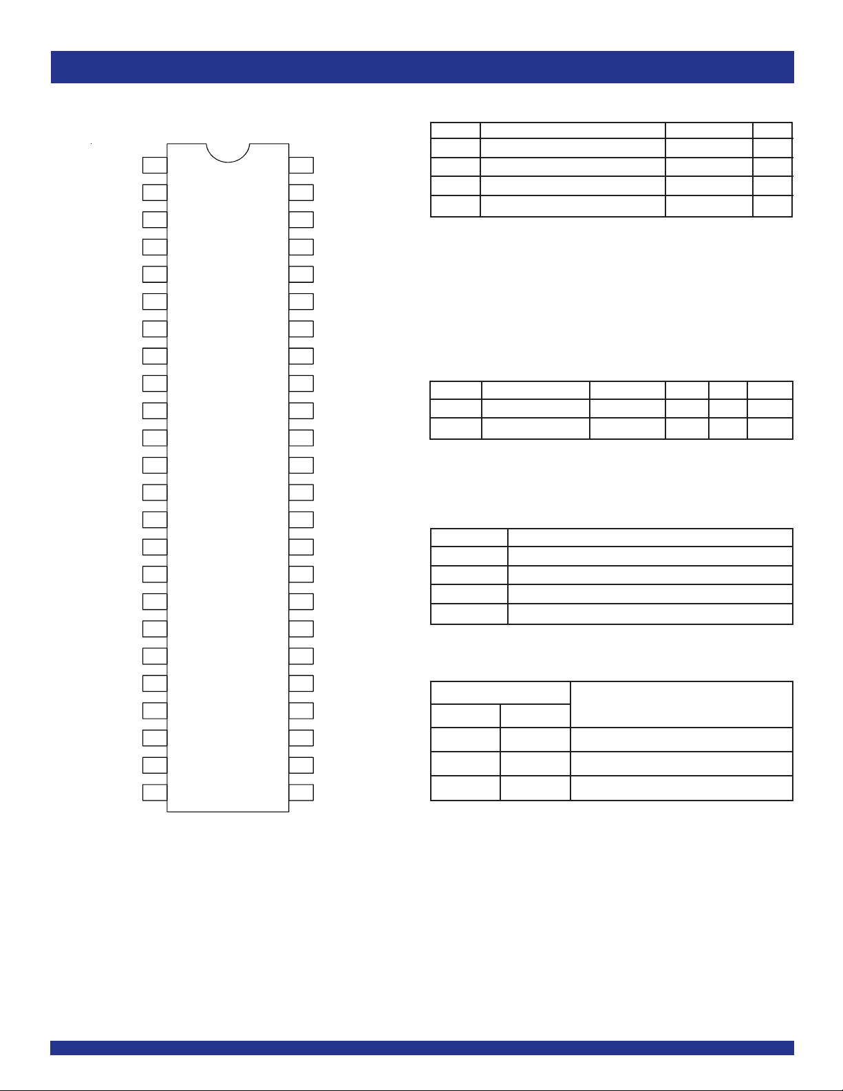
PIN CONFIGURATION
1DIR
1B1
1B2
GND
1B3
B4
1
VCC
1
2
3
4
5
6
7
48
47
46
45
44
43
42
1OE
1A1
1
GND
1A3
1
VCC
A2
A4
MILITARY AND INDUSTRIAL TEMPERATURE RANGES
(1)(1)
(1)
ABSOLUTE MAXIMUM RA TINGS
Symbol Description Max Unit
(2)
VTERM
VTERM
TSTG Storage Temperature –65 to +150 °C
I
OUT DC Output Current –60 to +120 mA
NOTES:
1. Stresses greater than those listed under ABSOLUTE MAXIMUM RATINGS may
cause permanent damage to the device. This is a stress rating only and functional
operation of the device at these or any other conditions above those indicated in
the operational sections of this specification is not implied. Exposure to absolute
maximum rating conditions for extended periods may affect reliability.
2. All device terminals except FCT162XXXT and FCT166XXXT (APort) Output and
I/O terminals.
3. Output and I/O terminals terminals for FCT162XXX and FCT166XXXT (A-Port).
Terminal Voltage with Respect to GND –0.5 to +7 V
(3)
Terminal Voltage with Respect to GND –0.5 to VCC+0.5 V
(1)(1)
1
B5
1
B6
GND
1
B7
1
B8
2
B1
2B2
GND
B3
2
2
B4
CC
V
2
B5
2
B6
GND
B7
2
8
9
10
11
12
13
14
15
16
17
18
19
20
21
22
41
40
39
38
37
36
35
34
33
32
31
30
29
28
27
A5
1
1
A6
GND
1
A7
1
A8
2
A1
2
A2
GND
2
A3
2
A4
VCC
A5
2
2
A6
GND
A7
2
CAPACITANCE (TA = +25°C, F = 1.0MHz)
Symbol Parameter
CIN Input Capacitance VIN = 0V 3.5 6 pF
C
OUT Output Capacitance VOUT = 0V 3.5 8 pF
NOTE:
1. This parameter is measured at characterization but not tested.
(1)
Conditions Typ. Max. Unit
PIN DESCRIPTION
Pin Names Description
xOE Output Enable Inputs (Active LOW)
xDIR Direction Control Inputs
xAx Side A Inputs or 3-State Outputs
xBx Side B Inputs or 3-State Outputs
FUNCTION TABLE
Inputs
xOE xDIR Outputs
L L Bus B Data to Bus A
(1)
DIR
2
2
B8
23
24
SSOP/ TSSOP/ TVSOP/ CERPACK
TOP VIEW
26
25
2
A8
2OE
L H Bus A Data to Bus B
H X High Z State
NOTE:
1. H = HIGH Voltage Level
L = LOW Voltage Level
X = Don’t Care
Z = High-Impedance
2
IDT54/74FCT16245T/AT/CT/ET
FAST CMOS 16-BIT BIDIRECTIONAL TRANSCEIVER
MILITARY AND INDUSTRIAL TEMPERATURE RANGES
DC ELECTRICAL CHARACTERISTICS OVER OPERATING RANGE
Following Conditions Apply Unless Otherwise Specified:
Industrial: TA = –40°C to +85°C, VCC = 5.0V ±10%; Military: TA = –55°C to +125°C, VCC = 5.0V ±10%
Symbol Parameter Test Conditions
V
IH Input HIGH Level Guaranteed Logic HIGH Level 2 — — V
(1)
Min. Typ.
VIL Input LOW Level Guaranteed Logic LOW Level — — 0.8 V
I
IH Input HIGH Current (Input pins)
Input HIGH Current (I/O pins)
I
IL Input LOW Current (Input pins)
Input LOW Current (I/O pins)
I
OZH High Impedance Output Current VCC = Max. VO = 2.7V — — ±1µA
IOZL (3-State Output pins)
(5)
(5)
VCC = Max. VI = VCC ——±1µA
(5)
(5)
(5)
VI = GND — — ±1
——±1
——±1
VO = 0.5V — — ±1
VIK Clamp Diode Voltage VCC = Min., IIN = –18mA — –0.7 –1.2 V
IOS Short Circuit Current VCC = Max., VO = GND
(3)
–80 –140 –250 mA
VH Input Hysteresis — — 100 — mV
CCL Quiescent Power Supply Current VCC = Max. — 5 500 µA
I
ICCH VIN = GND or VCC
ICCZ
(2)
Max. Unit
OUTPUT DRIVE CHARACTERISTICS
Symbol Parameter Test Conditions
IO Output Drive Current VCC = Max., VO = 2.5V
V
OH Output HIGH Voltage VCC = Min. IOH = –3mA, –2.5 3.5 — V
IN = VIH or VIL IOH = –12mA MIL 2.4 3.5 — V
V
(1)
(3)
OH = –15mA IND
I
I
OH = –24mA MIL 2 3 — V
IOH = –32mA IND
(4)
Min. Typ.
–50 — –180 mA
VOL Output LOW Voltage VCC = Min. IOL = 48mA MIL — 0.2 0.55 V
VIN = VIH or VIL IOL = 64mA IND
OFF Input/Output Power Off Leakage
I
NOTES:
1. For conditions shown as Min. or Max., use appropriate value specified under Electrical Characteristics for the applicable device type.
2. Typical values are at VCC = 5.0V, +25°C ambient.
3. Not more than one output should be shorted at one time. Duration of the test should not exceed one second.
4. Duration of the condition can not exceed one second.
5. The test limit for this parameter is ±5µA at TA = –55°C.
(5)
VCC = 0V, VIN or VO ≤ 4.5V — — ±1 µA
(2)
Max. Unit
3
 Loading...