


Integrated Device Technology Inc IDT49FCT3805AD, IDT49FCT3805ADB, IDT49FCT3805AE, IDT49FCT3805AEB, IDT49FCT3805AL Datasheet
...
Integrated Device Technology, Inc.
FAST CMOS
BUFFER/CLOCK DRIVER
FEATURES:
• 0.5 MICRON CMOS Technology
• Guaranteed low skew < 500ps (max.)
• Very low duty cycle distortion < 1.0ns (max.)
• Very low CMOS power levels
• TTL compatible inputs and outputs
• Inputs can be driven from 3.3V or 5V components
• Two independent output banks with 3-state control
• 1:5 fanout per bank
• ‘Heartbeat’ monitor output
• Available in DIP, SOIC, SSOP, QSOP, Cerpack and
LCC packages
• Military product compliant to MIL-STD-883, Class B
•V
CC = 3.3V ± 0.3V
DESCRIPTION:
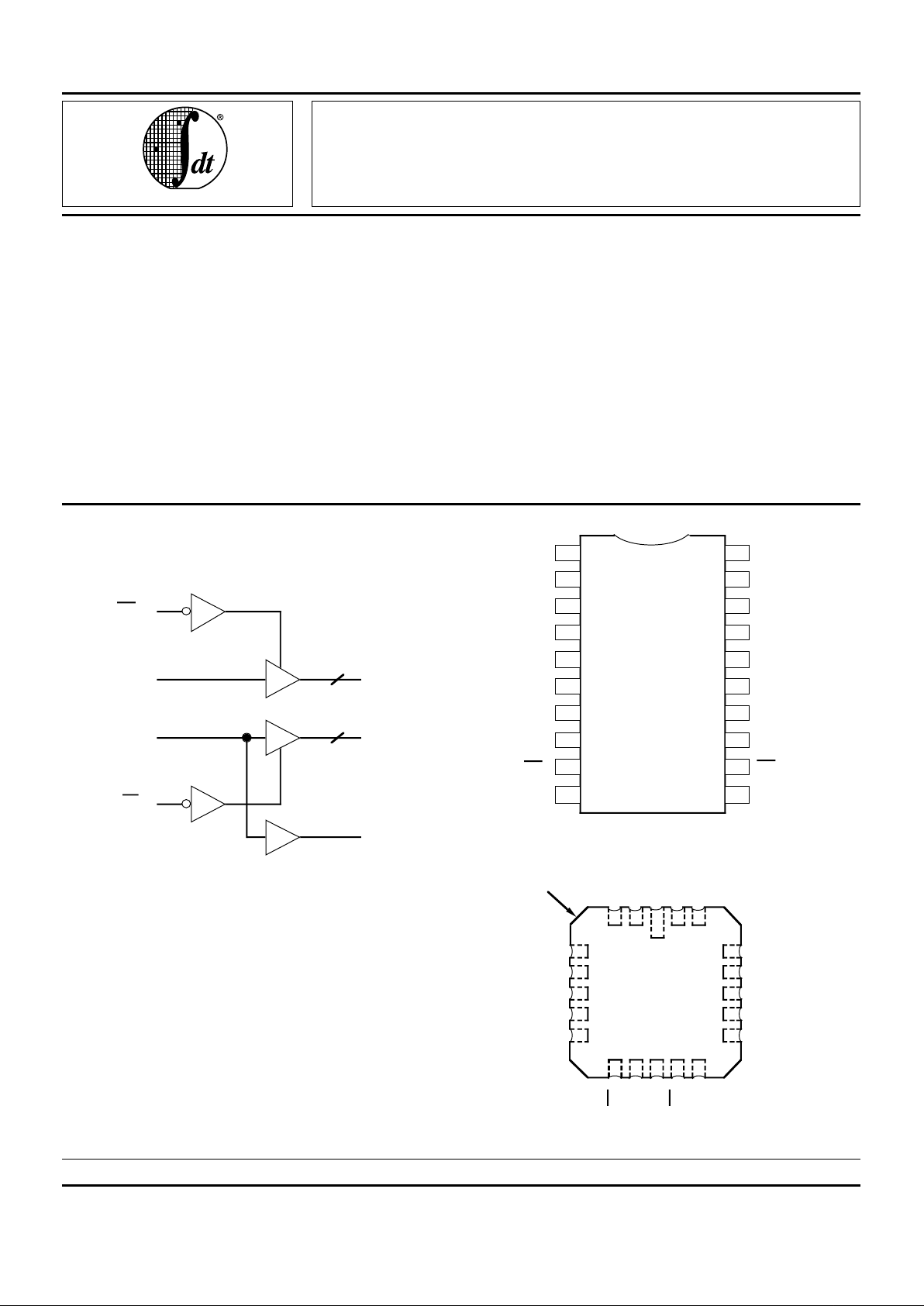
The FCT3805/A is a 3.3 volt, non-inverting clock driver built
using advanced dual metal CMOS technology. The device
consists of two banks of drivers, each with a 1:5 fanout and its
own output enable control. The device has a "heartbeat"
monitor for diagnostics and PLL driving. The MON output is
identical to all other outputs and complies with the output
specifications in this document. The FCT3805/A offers low
capacitance inputs with hysteresis.
The FCT3805/A is designed for high speed clock distribution where signal quality and skew are critical. The FCT 3805
also allows single point-to-point transmission line driving in
applications such as address distribution, where one signal
must be distributed to multiple receivers with low skew and
high signal quality.
IDT49FCT3805/A
MILITARY AND COMMERCIAL TEMPERATURE RANGES OCTOBER 1995
1996 Integrated Device Technology, Inc. 9.5 DSC-3102/4
1
The IDT logo is a registered trademark of Integrated Device Technology, Inc.
OEA
5
5
INA
INB
OEB
OA1-OA5
OB1-OB5
MON
3102 drw 01
3102 drw 02
3102 drw 03
FUNCTIONAL BLOCK DIAGRAM
PIN CONFIGURATIONS
INDEX
LCC
TOP VIEW
3 2 20 19
1
4
5
6
7
8
18
17
16
15
14
910111213
L20-2
OA3
GNDA
OA4
OA5
GNDQ
OB2
OB3
GNDB
OB4
OB5
OEA
INA
INB
OEB
MON
OA2
OA1
VCCA
VCCB
OB1
OB
1
OA
1
OA
3
GND
A
OA
4
OA
5
OA
2
OE
A
IN
A
OB
2
OB
3
GND
B
OB
4
MON
IN
B
OB
5
OE
B
V
CCB
1
2
3
4
5
6
7
8
9
10
11
12
13
14
15
16
17
18
19
20
DIP/SOIC/SSOP/QSOP/CERPACK
TOP VIEW
P20-1
D20-1
SO20-2
SO20-7
SO20-8
&
E20-1
V
CCA
GND
Q
IDT49FCT3805/A
FAST CMOS BUFFER/CLOCK DRIVER MILITARY AND COMMERCIAL TEMPERATURE RANGES
9.5 2
NOTE:
1. This parameter is measured at characterization but not tested.
PIN DESCRIPTION FUNCTION TABLE
(1)
3102 tbl 01
NOTE: 3102 tbl 02
1. H = HIGH, L = LOW, Z = High Impedance
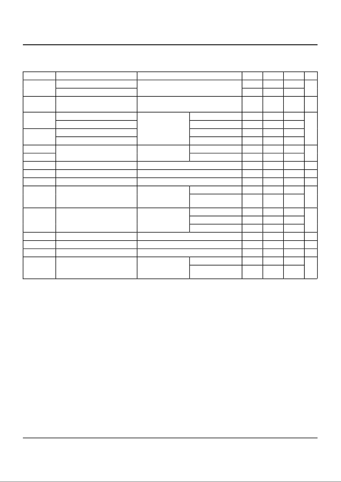
ABSOLUTE MAXIMUM RATINGS
(1)
CAPACITANCE (TA = +25°C, f = 1.0MHz)
3102 lnk 04
Symbol Rating Commercial Military Unit
VTERM
(2)
Terminal Voltage
with Respect to
GND
–0.5 to +4.6 –0.5 to +4.6 V
VTERM
(3)
Terminal Voltage
with Respect to
GND
–0.5 to +7.0 –0.5 to +7.0 V
VTERM
(4)
Terminal Voltage
with Respect to
GND
–0.5 to V
CC
+ 0.5
–0.5 to VCC
+ 0.5
V
TA Operating
Temperature
0 to +70 –55 to +125 °C
TBIAS Temperature
Under Bias
–55 to +125 –65 to +135 °C
TSTG Storage
Temperature
–55 to +125 –65 to +150 °C
IOUT DC Output
Current
–60 to +60 –60 to +60 mA
NOTES:
1. Stresses greater than those listed under ABSOLUTE MAXIMUM RATINGS
may cause permanent damage to the device. This is a stress rating only
and functional operation of the device at these or any other conditions
above those indicated in the operational sections of this specification is
not implied. Exposure to absolute maximum rating conditions for extended periods may affect reliability.
2. Vcc terminals.
3. Input terminals.
4. Output and I/O terminals.
3102 lnk 03
Symbol Parameter
(1)
Conditions Typ. Max. Unit
CIN Input
Capacitance
VIN = 0V 3.5 5.0 pF
COUT Output
Capacitance
VOUT = 0V 3.5 5.0 pF
Pin Names Description
OEA,
OE
B
3-State Output Enable Inputs (Active LOW)
INA, IN
B
Clock Inputs
OAn, OB
n
Clock Outputs
MON Monitor Output
Inputs Outputs
OE
OE
A,
OE
OE
B INA, INB OAn, OBn MON
LLLL
LHHH
HLZL
HH ZH
IDT49FCT3805/A
FAST CMOS BUFFER/CLOCK DRIVER MILITARY AND COMMERCIAL TEMPERATURE RANGES
9.5 3
DC ELECTRICAL CHARACTERISTICS OVER OPERATING RANGE
Following Conditions Apply Unless Otherwise Specified:
Commercial: TA = 0°C to +70°C, VCC = 3.3V ± 0.3V; Military: TA = –55°C to +125°C, VCC = 3.3V ± 0.3V
3102 lnk 05
NOTES:
1. For conditions shown as Max. or Min., use appropriate value specified under Electrical Characteristics for the applicable device type.
2. Typical values are at Vcc = 3.3V, +25°C ambient.
3. Not more than one output should be tested at one time. Duration of the test should not exceed one second.
4. This parameter is guaranteed but not tested.
5. V
OH = VCC -0.6V at rated current.
6. The test limit for this parameter is ±5µA at TA = –55°C.
Symbol Parameter Test Conditions
(1)
Min. Typ.
(2)
Max. Unit
VIH Input HIGH Level (Input pins) Guaranteed Logic HIGH Level 2.0 — 5.5 V
Input HIGH Level (I/O pins) 2.0 — VCC+0.5
VIL Input LOW Level Guaranteed Logic LOW Level –0.5 — 0.8 V
(Input and I/O pins)
II H Input HIGH Current (Input pins)
(6)
VCC = Max. VI = 5.5V — — ±1 µA
Input HIGH Current (I/O pins)
(6)
VI = VCC ——±1
II L Input LOW Current (Input pins)
(6)
VI = GND — — ±1
Input LOW Current (I/O pins)
(6)
VI = GND — — ±1
IOZH High Impedance Output Current VCC = Max. VO = VCC ——±1µA
IOZL (3-State Output pins)
(6)
VO = GND — — ±1
VIK Clamp Diode Voltage VCC = Min., IIN = –18mA — –0.7 –1.2 V
IODH Output HIGH Current VCC = 3.3V, VIN = VIH or VIL, VO = 1.5V
(3)
–36 –60 –110 mA
IODL Output LOW Current VCC = 3.3V, VIN = VIH or VIL, VO = 1.5V
(3)
50 90 200 mA
VOH Output HIGH Voltage VCC = Min. IOH = –0.1mA VCC–0.2 — — V
VIN = VIH or VIL IOH = –6mA MIL.
I
OH = –8mA COM'L.
2.4
(5)
3.0 —
VOL Output LOW Voltage VCC = Min. IOL = 0.1mA — — 0.2 V
VIN = VIH or VIL IOL = 16mA — 0.2 0.4
IOL = 24mA — 0.3 0.50
IOFF Input Power Off Leakage
(6)
VCC = 0V, VIN ≤ 4.5V — — ±1 µA
IOS Short Circuit Current
(4)
VCC = Max., VO = GND
(3)
–60 –135 –240 mA
VH Input Hysteresis — — 150 — mV
ICCL Quiescent Power Supply Current VCC = Max., COM'L. — 0.1 10 µA
ICCH
ICCZ
VIN = GND or VCC MIL. — 0.1 100