ICS502
LOCO™ PLL Clock Multiplier
Description
The ICS502 LOCO™ is the most cost effective
way to generate a high quality, high frequency
clock output and a reference from a low frequency
crystal or clock input. The name LOCO stands for
LOw Cost Oscillator, as it is designed to replace
crystal oscillators in most electronic systems. Using
Phase-Locked-Loop (PLL) techniques, the device
uses a standard fundamental mode, inexpensive
crystal to produce output clocks up to 160 MHz.
Stored in the chip’s ROM is the ability to generate
6 different multiplication factors, allowing one
chip to output many common frequencies (see
page 2).
Features
• Packaged as 8 pin SOIC or die
• ICS’ lowest cost PLL clock plus reference
• Zero ppm multiplication error
• Easy to cascade with other 5xx series
• Input crystal frequency of 5 - 27 MHz
• Input clock frequency of 2 - 50 MHz
• Output clock frequencies up to 160 MHz
• Low jitter - 50 ps one sigma
• Compatible with all popular CPUs
• Duty cycle of 45/55 up to 160 MHz
• Operating voltages of 3.0 to 5.5V
• Industrial temperature version available
• 25mA drive capability at TTL levels
• Advanced, low power CMOS process
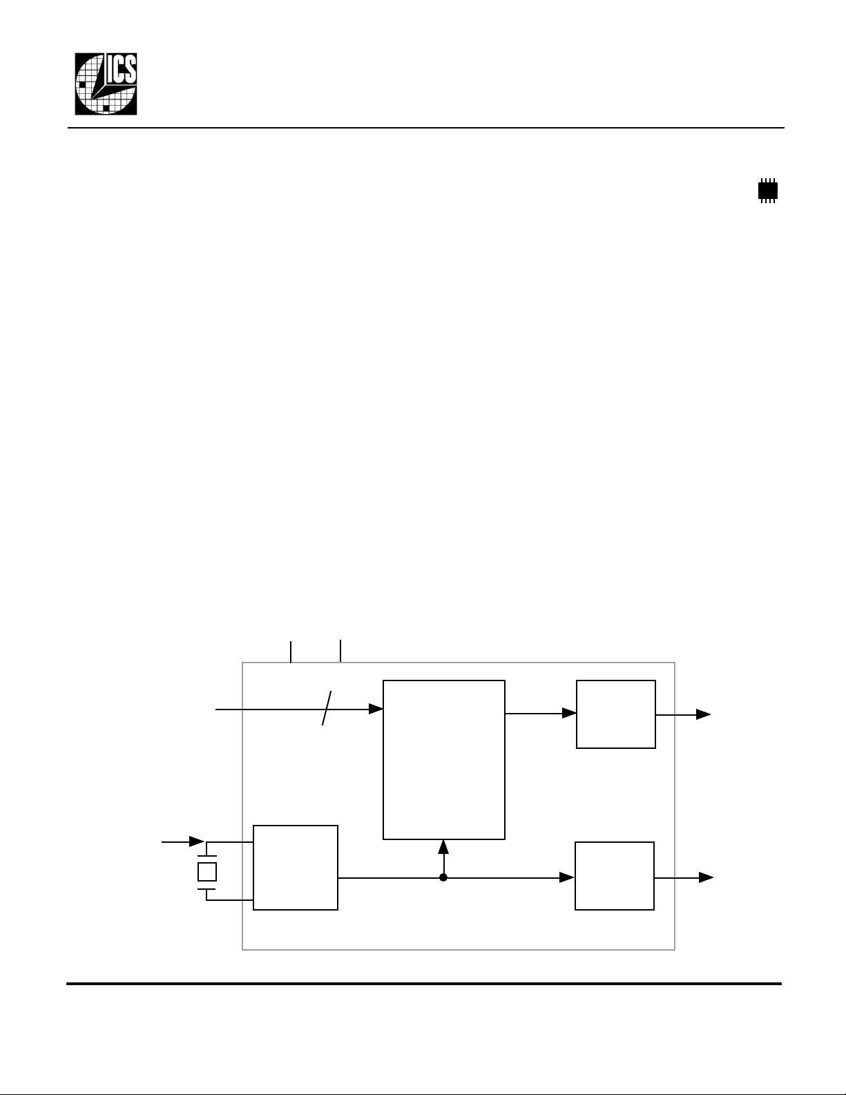
Block Diagram
S1, S0
crystal
or clock
X1/ICLK
X2
VDD GND
2
Crystal
Oscillator
PLL
Clock
Synthesis
and Control
Circuitry
Output
Buffer
Output
Buffer
CLK
REF
MDS 502 D 1 Revision 111000
Integrated Circuit Systems, Inc. • 525 Race Street • San Jose •CA•95126•(408) 295-9800tel • www.icst.com

ICS502
LOCO™ PLL Clock Multiplier
Pin Assignment
X1/ICLK
VDD
GND
REF
1 8
2
3
4
X2
7
S1
6
S0
5
CLK
Clock Decoding Table (MHz)
S1 S0 CLK
0 0 x2
0 1 x5
M 0 x3
M 1 x3.33
1 0 x4
1 1 x2.5
Minimum input frequency for all
selections is per table on page 3.
0 = connect directly to ground.
1 = connect directly to VDD.
M = leave unconnected (floating).
Common Output Frequencies Examples (MHz)
Output 20 25 30 32 33.33 37.5 40 48 50 54 60
Input 10 10 10 16 10 15 20 16 20 13.5 20
Selection (S1, S0) 0, 0 1, 1 M, 0 0, 0 M, 1 1, 1 0, 0 M, 0 1, 1 1, 0 M, 0
Output 64 66.66 72 75 80 81 90 100 108 120 135
Input 16 20 24 15 20 27 27 20 27 24 27
Selection (S1, S0) 1, 0 M, 1 M, 0 0, 1 1, 0 M, 0 M, 1 0, 1 1, 0 0, 1 0, 1
Note that all of the above outputs are achieved by using an inexpensive 10MHz to 27MHz crystal.
Consult MicroClock/ICS on how to achieve other output frequencies.
Pin Descriptions
Number Name Type Description
1 X1/ICLK I Crystal connection or clock input.
2 VDD P Connect to +3.3V or +5V.
3 GND P Connect to ground.
4 REF O Buffered crystal oscillator output clock.
5 CLK O Clock output per Table above.
6 S0 I Select 0 for output clock. Connect to GND or VDD.
7 S1 TI Select 1 for output clock. Connect to GND or VDD or float.
8 X2 O Crystal connection. Leave unconnected for clock input.
Key: I = Input, TI = Tri-Level Input, O = output, P = power supply connection
MDS 502 D 2 Revision 111000
Integrated Circuit Systems, Inc. • 525 Race Street • San Jose •CA•95126•(408) 295-9800tel • www.icst.com
 Loading...