Integrated
Circuit
Systems, Inc.
ICS9250-23
Third party brands and names are the property of their respective owners.
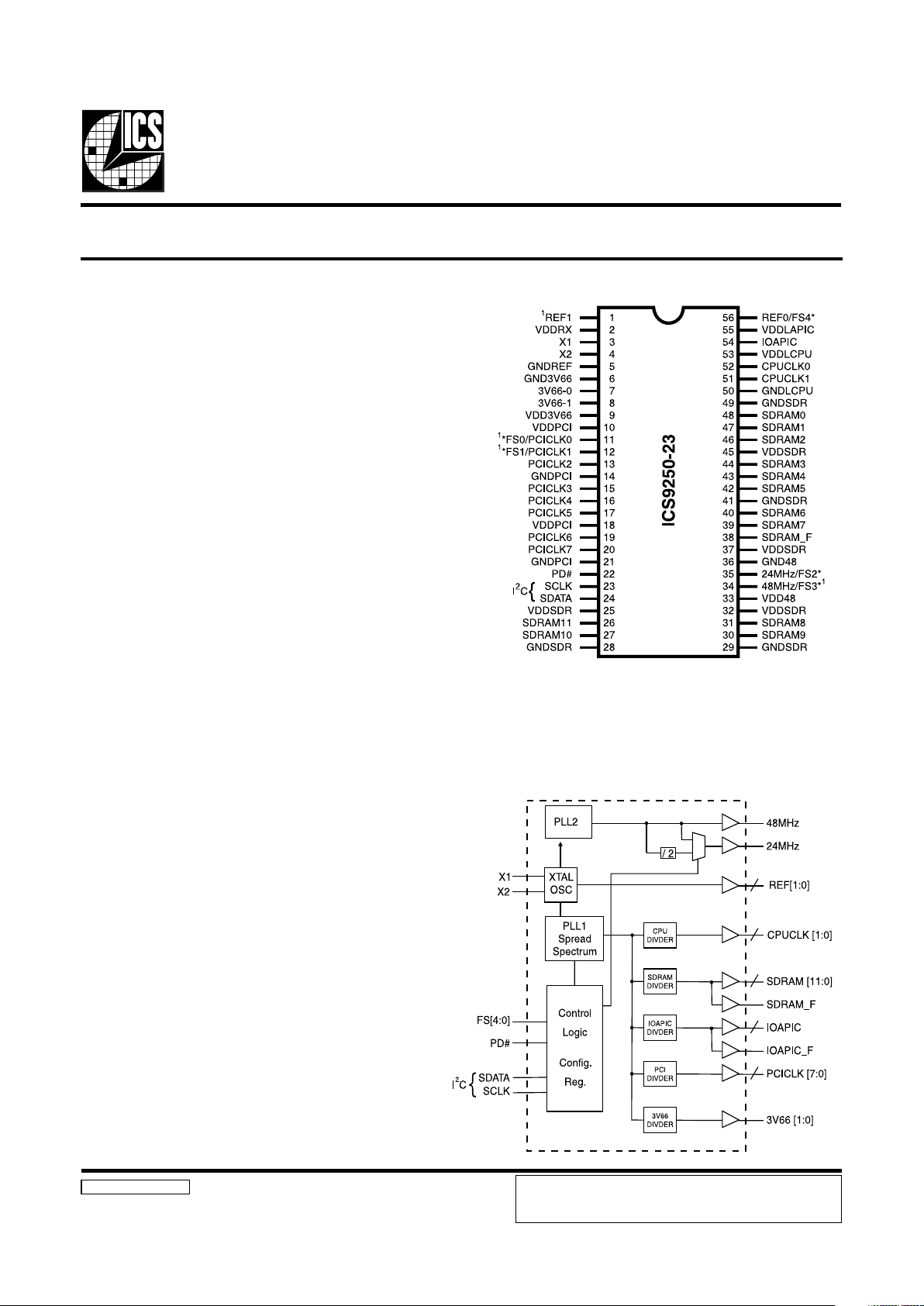
Block Diagram
9250-23 Rev A 4/3/01
Pin Configuration
Recommended Application:
810/810E type chipset
Output Features:
• 2 - CPUs @ 2.5V, up to 166MHz.
• 13 - SDRAM @ 3.3V, up to 166MHz.
• 2 - 3V66 @ 3.3V, 2x PCI MHz.
• 8 - PCI @3.3V.
• 1 - 48MHz, @3.3V fixed.
• 1 - 24MHz @ 3.3V
• 2 - REF @3.3V, 14.318MHz.
Features:
• Up to 166MHz frequency support
• Support power management through PD#.
• Spread spectrum for EMI control (± 0.25%)
center spread.
• Uses external 14.318MHz crystal
• FS pins for frequency select
Key Specifications:
• CPU Output Jitter: <250ps
• IOAPIC Output Jitter: <500ps
• 48MHz, 3V66, PCI Output Jitter: <500ps
• Ref Output Jitter. <1000ps
• CPU Output Skew: <175ps
• PCI Output Skew: <500ps
• 3V66 Output Skew <175ps
• For group skew timing, please refer to the
Group Timing Relationship Table.
Frequency Generator & Integrated Buffers for Celeron & PII/III™
56-Pin 300 mil SSOP
1. These pins will have 2X drive strength.
* 120K ohm pull-up to VDD on indicated inputs.
Power Groups
GNDREF, VDDREF = REF, Crystal
GND3V66, VDD3V66 = 3V66
GNDPCI, VDDPCI = PCICLKs
GNDCOR, VDDCOR = PLLCORE
GND48, VDD48 = 48
GNDSDR, VDDSDR = SDRAM
GNDLCPU, VDDLCPU = CPUCLK
GNDLPCI, VDDLAPIC = IOAPIC
ICS reserves the right to make changes in the device data identified in
this publication without further notice. ICS advises its customers to
obtain the latest version of all device data to verify that any
information being relied upon by the customer is current and accurate.

2
ICS9250-23
Third party brands and names are the property of their respective owners.
General Description
Pin Configuration
NIP
REBMUN
EMANNIPEPYTNOITPIRCSED
11FERTUO.tuptuokcolcecnereferzHM813.41,V3.3
,52,81,01,9,2
54,73,33,23
DDVRWP.ylppusrewopV3.3
31XNI
kcabdeefdna)Fp33(pacdaollanretnisah,tupnilatsyrC
.2Xmorfrotsiser
42XTUO
daollanretnisaH.zHM813.41yllanimon,tuptuolatsyrC
)Fp33(pac
,12,41,6,5
,63,92,82
94,14
DNGRWP.ylppusV3.3rofsnipdnuorG
7,8]0:1[66V3TUO.BUHrofstuptuokcolczHM66dexiFV3.3
11
0KLCICP
1
TUO.SKLCUPCsuonorhcnyShtiw,stuptuokcolcICPV3.3
0SFNI.norewoptadehctaltupnI.tibtcelesycneuqerftupnicigoL
21
1KLCICP
1
TUO.SKLCUPCsuonorhcnyShtiw,stuptuokcolcICPV3.3
1SFNI.norewoptadehctaltupnI.tibtcelesycneuqerftupnicigoL
,61,71,91,02
31,51
]2:7[KLCICPTUO.SKLCUPCsuonorhcnyShtiw,stuptuokcolcICPV3.3
22#DPNI
otniecivedehtnwodrewopotdesuniptupniwolevitcasuonorhcnysA
dnaOCVehtdnadelbasideraskcolclanretniehT.etatsrewopwola
ebtonlliwnwodrewopehtfoycnetalehT.deppotseralatsyrceht
.sm3nahtretaerg
32KLCSNIIfotupnikcolC
2
.tupniC
42ATADSO/IIrofnipataD
2
.tnarelotV5yrtiucricC
43
zHM84TUO.BSUroftuptuokcolczHM84dexiFV3.3
3SFNI.norewoptadehctaltupnI.tibtcelesycneuqerftupnicigoL
53
2SFNI.norewoptadehctaltupnI.tibtcelesycneuqerftupnicigoL
zHM42TUO.tuptuozHM42dexifV3.3
83F_MARDSTUOIybdetceffatonMARDSzHM001gninnureerfV3.3
2
.C
,13,03,72,62
,34,24,04,93
84,74,64,44
]0:11[MARDSTUO
ffodenrutebnacstuptuoMARDSllA.zHM001gninnurtuptuoV3.3
Ihguorht
2
.C
05LDNGRWP.CIPA&UPCrofylppusrewopV5.2rofdnuorG
25,15]0:1[KLCUPCTUO.snipSFmorfdeviredycneuqerftuptuO.tuptuokcolcsubtsoHV5.2
55,35LDDVRWP.CIPAOI,UPCrofylppyusrewopV5.2
45CIPAOITUO.zHM76.61tagninnurstuptuokcolcV5.2
65
4SFNI.norewoptadehctaltupnI.tibtcelesycneuqerftupnicigoL
0FER
1
TUO.tuptuokcolcecnereferzHM813.41,V3.3
The ICS9250-23 is a single chip clock solution for desktop designs using the 810/810E style chipset. It provides all necessary
clock signals for such a system.
Spread spectrum may be enabled through I
2
C programming. Spread spectrum typically reduces system EMI by 8dB to
10dB. This simplifies EMI qualification without resorting to board design iterations or costly shielding. The ICS9250-23
employs a proprietary closed loop design, which tightly controls the percentage of spreading over process and temperature
variations.
Serial programming I
2
C interface allows changing functions, stop clock programming and frequency selection.

3
ICS9250-23
Third party brands and names are the property of their respective owners.
Frequency Selection
Clock Enable Configuration
4SF3SF2SF1SF0SF
UPC
zHM
MARDS
zHM
zHM66V3
ICP
zHM
zHMCIPAOI
00000 00.9605.30100.9605.4352.71
0000 1 00.0700.50100.0700.5305.71
00010 00.1705.60100.1705.5357.71
00011 09.6653.00109.6654.3337.61
00100 00.2700.80100.2700.6300.81
00101 00.5705.21100.5705.7357.81
00110 06.6709.41106.6704.8302.91
00111 00.5805.72100.5805.2452.12
01000 00.8600.20100.8600.4300.71
01001 00.4700.11100.4700.7305.81
01010 00.04100.04100.0700.5305.71
01011 33.33133.33176.6633.3376.61
01100 00.05100.05100.5705.7357.81
01101 00.55100.55105.7757.8383.91
01110 00.66100.66100.3805.1457.22
01111 00.66100.66100.11108.5509.72
10000 77.11177.11125.4762.7336.81
1000 1 87.40187.40168.9639.4364.71
100 10 15.90115.90110.3705.6352.81
100 1 1 09.00109.00172.7636.3328.61
10 100 00.71100.71105.8752.9336.91
10 10 1 57.32157.32105.2852.1426.02
10 1 10 33.33133.33198.8844.4422.22
10111 05.24105.24100.5905.7457.32
11000 00.63152.20105.8652.4331.71
11001 00.04100.50100.0700.5305.71
11010 00.34105.70100.2700.6300.81
11011 09.33186.00154.7637.3368.61
11100 76.64100.01133.3776.6333.81
11101 33.94100.21176.4733.7376.81
11110 03.35192.51142.7726.8303.91
11111 76.66123.52143.3876.1438.02
#DPKLCUPCMARDSCIPAOIzHM66KLCICP
,FER
zHM84
csOsOCV
0WOLWOLWOLWOLWOLWOLFFOFFO
1NONONONONONONONO

4
ICS9250-23
Third party brands and names are the property of their respective owners.
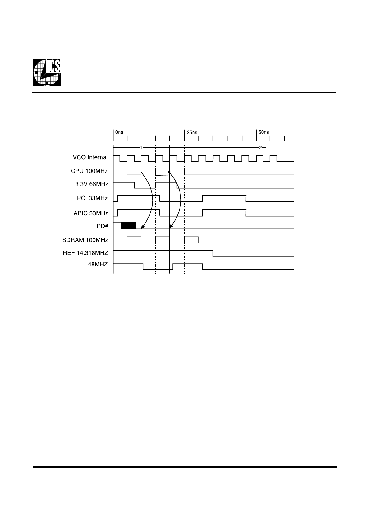
Power Down Waveform
Note
1. After PD# is sampled active (Low) for 2 consective rising edges of CPUCLKs, all
the output clocks are driven Low on their next High to Low tranistiion.
2. Power-up latency <3ms.
3. Waveform shown for 100MHz

5
ICS9250-23
Third party brands and names are the property of their respective owners.
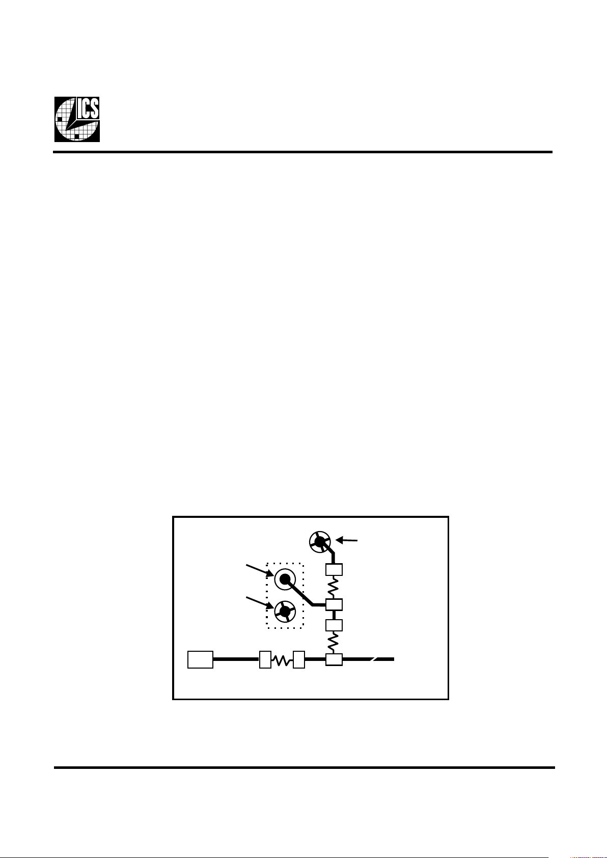
Fig. 1
Via to
VDD
Clock trace to load
Series Term. Res.
Programming
Header
Via to Gnd
Device
Pad
2K W
8.2K W
Shared Pin Operation Input/Output Pins
The I/O pins designated by (input/output) serve as dual
signal functions to the device. During initial power-up, they
act as input pins. The logic level (voltage) that is present on
these pins at this time is read and stored into a 5-bit internal
data latch. At the end of Power-On reset, (see AC
characteristics for timing values), the device changes the
mode of operations for these pins to an output function. In
this mode the pins produce the specified buffered clocks to
external loads.
To program (load) the internal configuration register for these
pins, a resistor is connected to either the VDD (logic 1) power
supply or the GND (logic 0) voltage potential. A 10 Kilohm
(10K) resistor is used both to provide the solid CMOS
programming voltage needed during the power-up
programming period and to provide an insignificant load on
the output clock during the subsequent operating period.
Figure 1 shows a means of implementing this function when
a switch or 2 pin header is used. When no jumper is installed
the pin will be pulled high. With the jumper in place the pin
will be pulled low. If programmability is not necessary, then
only a single resistor is necessary. The programming resistors
should be located close to the series termination resistor to
minimize the current loop area. It is more important to locate
the series termination resistor close to the driver than the
programming resistor.
 Loading...