

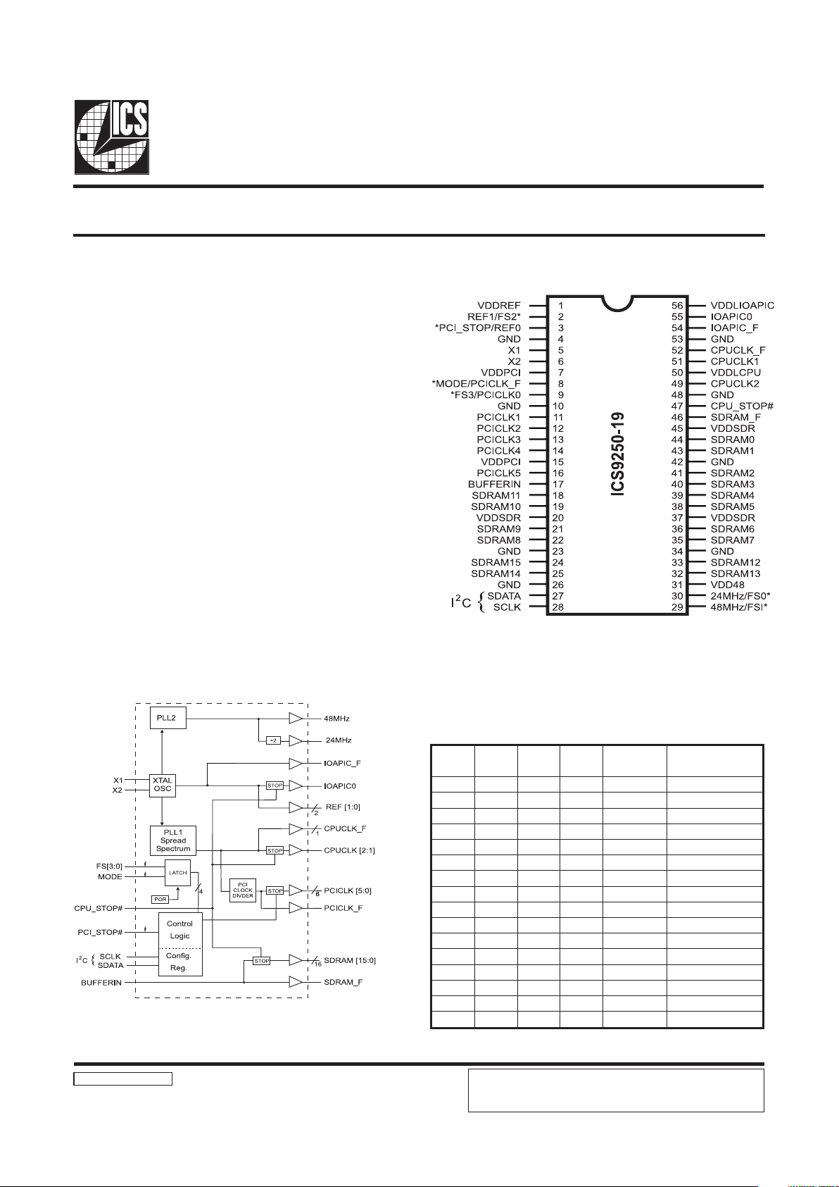
ICS9250-19
Third party brands and names are the property of their respective owners.
Integrated
Circuit
Systems, Inc.
Block Diagram
Frequency Generator & Integrated Buffers for Celeron & PII/III™
9250-19 Rev C 4/12/01
Functionality
Pin Configuration
Recommended Application:
BX, Appollo Pro 133 type of chip set.
Output Features:
• 3 - CPUs @2.5V, up to 150MHz.
• 17 - SDRAM @ 3.3V, up to 150MHz.
• 7 - PCI @3.3V
• 2 - IOAPIC @ 2.5V
• 1 - 48MHz, @3.3V fixed.
• 1 - 24MHz @ 3.3V
• 2 - REF @3.3V, 14.318MHz.
Features:
• Up to 150MHz frequency support
• Support power management: CPU, PCI, stop and Power
down Mode form I
2
C programming.
• Spread spectrum for EMI control (0 to -0.5%, ± 0.25%).
• Uses external 14.318MHz crystal
Key Specifications:
• CPU – CPU: <175ps
• CPU – PCI: 1 - 4ns
• PCI – PCI: <500ps
• SDRAM - SDRAM: <250ps
56-Pin SSOP
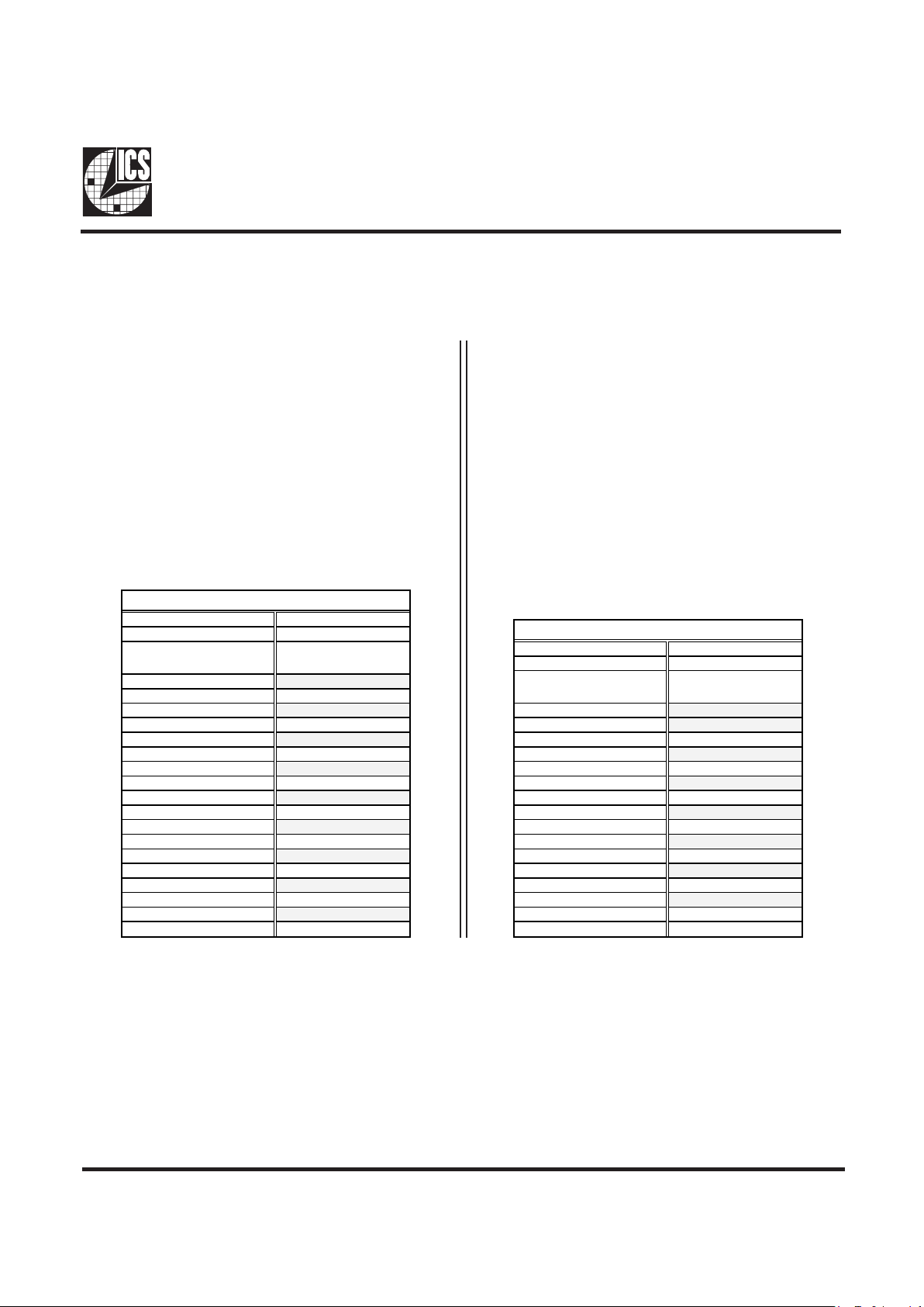
* Internal Pull-up Resistor of 240K to 3.3V on indicated inputs
** Internal Pull-down resistor of 240K to GND on indicated inputs.
3SF2SF1SF0SF
UPC
)zHM(
)zHM(KLCICP
1111 331)4/UPC(3.33
1110 421)4/UPC(13
110 1 051)4/UPC(5.73
1100 041)4/UPC(53
10 11 501)3/UPC(53
10 10 011)3/UPC(76.63
1001 511)3/UPC(33.83
1000 021)3/UPC(00.04
0111 0.001)3/UPC(34.33
0110 331)3/UPC(33.44
0101 211)3/UPC(33.73
0100 301)2/UPC(33.43
0011 6.66)2/UPC(04.33
0010 3.38)2/UPC(56.14
0001 57)2/UPC(5.73
0000 421)2/UPC(33.14
ICS reserves the right to make changes in the device data identified in
this publication without further notice. ICS advises its customers to
obtain the latest version of all device data to verify that any
information being relied upon by the customer is current and accurate.

2
ICS9250-19
Third party brands and names are the property of their respective owners.
Pin Configuration
Notes:
1: Bidirectional input/output pins, input logic levels are latched at internal power-on-reset. Use 10Kohm resistor
to program logic Hi to VDD or GND for logic low.
REBMUNNIPEMANNIPEPYTNOITPIRCSED
2
1FERTUOtuptuokcolcecnereferzHM813.41
2SF
1
NIICPDDVotpu-llupsaH.tupnitcelesycneuqerfdehctaL
3
0FERTUOtuptuokcolcecnereferzHM813.41
#POTS_ICPNI
.wolnehwlevel"0"cigolta]1:5[KLCICPstlaH
)0=EDOM,elibomni(
,24,43,62,32,01,4
35,84
DNGRWP.dnuorG
51XNI.)Fp33lanimon(,pacdaollanretnisaH.tupnizHM813.41
62XTUO
kcabdeefdna)Fp33(pacdaollanretnisaH.tuptuolatsyrC
1Xotrotsiser
8
F_KLCICPTUO#POTS_ICPybdetcefatonkcolcSUBgninnureerF
EDOM
1
NI
nehw#POTS_ICPot3nipstrevnoC.tcelesEDOMroftupnidehctaL
.tnemeganamrewoprofwol
9
3SFNInwod-llup,tupnitcelesycneuqerfdehctaL
0KLCICPTUO#POTS_ICPybdetcefatonkcolcSUBgninnureerF
11,21,31,41,61]1:5[KLCICPTUO.stuptuOkcolCICP
71NIREFFUBNIsreffuBroftupnI
72ATADSNII(.tropgifnoclairesrofniatadlaireS
2
)C
82KLCSNII(.tropgifnoclairesroftupnikcolC
2
)C
03
zHM42TUO.DFroO/IrepuSroftuptuokcolczHM42
0SF
1
NI.4DDVotpu-llupsaH.tupnitcelesycneuqerfdehctaL
92
zHM84TUO.BSUroftuptuokcolczHM84
1SF
1
NI.2DDVotpu-llupsaH.tupnitcelesycneuqerfdehctaL
,02,51,7,1
,1354,73
,FERDDV,ICPDDV
84DDV,RDSDDV
RWP.noitcnufrofspuorgrewopees,ylppusrewopV3.3lanimoN
,81,33,23,52,42
,63,53,22,12,91
,34,14,04,93,83
44
]0:51[MARDSTUOskcolcMARDS
64F_MARDSTUO#POTS_UPCybdetceffatoNkcolcMARDSgninnureerF
74#POTS_UPCNI
KLCUPCstlaH]0:51[MARDS,0CIPAOI,]1:2[
.wolnehwlevel"0"cigoltaskcolc
65,05
,UPCLDDV
CIPAOILDDV
RWP.lanimonV5.2,ylppusrewopreffubkcolcCIPAOIdnaUPC
550CIPAOITUO1LDDVybderewoP)zHM813.41(.tuptuokcolcCIPAOI
94,15]1:2[KLCUPCTUO)zHM6.66ro06(2LDDVybderewoP.skcolctuptuOUPC
25F_KLCUPCTUO.#POTS_UPCehtytdetceffatoN.kcolctuptuoUPCgninnureerF
45F_CIPAOITUO
gninnureerF.tuptuokcolcCIPAOI#POTS_UPCehtybdetceffatoN
1LDDVybderewoP)zHM81813.41(

3
ICS9250-19
Third party brands and names are the property of their respective owners.
General Description
The ICS9250-19 is the single chip clock solution for Desktop/designs using BX, Appollo Pro 133 type of chip sets. It provides
all necessary clock signals for such a system.
Spread spectrum may be enabled through I
2
C programming. Spread spectrum typically reduces system EMI by 8dB to
10dB. This simplifies EMI qualification without resorting to board design iterations or costly shielding. The ICS9250-19
employs a proprietary closed loop design, which tightly controls the percentage of spreading over process and temperature
variations.
Serial programming I
2
C interface allows changing functions, stop clock programming and frequency selection.
Mode Pin - Power Management Input Control
EDOM
)tupnIdehctaL(
0
#POTS_ICP
)tupnI(
1
0FER
)tuptuO(
4
ICS9250-19
Third party brands and names are the property of their respective owners.
1. The ICS clock generator is a slave/receiver, I2C component. It can read back the data stored in the latches for
verification. Read-Back will support Intel PIIX4 "Block-Read" protocol.
2. The data transfer rate supported by this clock generator is 100K bits/sec or less (standard mode)
3. The input is operating at 3.3V logic levels.
4. The data byte format is 8 bit bytes.
5. To simplify the clock generator I
2
C interface, the protocol is set to use only "Block-Writes" from the controller. The
bytes must be accessed in sequential order from lowest to highest byte with the ability to stop after any complete byte
has been transferred. The Command code and Byte count shown above must be sent, but the data is ignored for those
two bytes. The data is loaded until a Stop sequence is issued.
6. At power-on, all registers are set to a default condition, as shown.
General I2C serial interface information
The information in this section assumes familiarity with I2C programming.
For more information, contact ICS for an I
2
C programming application note.
How to Write:
• Controller (host) sends a start bit.
• Controller (host) sends the write address D2
(H)
• ICS clock will acknowledge
• Controller (host) sends a dummy command code
• ICS clock will acknowledge
• Controller (host) sends a dummy byte count
• ICS clock will acknowledge
• Controller (host) starts sending first byte (Byte 0)
through byte 5
• ICS clock will acknowledge each byte one at a time.
• Controller (host) sends a Stop bit
How to Read:
• Controller (host) will send start bit.
• Controller (host) sends the read address D3
(H)
• ICS clock will acknowledge
• ICS clock will send the byte count
• Controller (host) acknowledges
• ICS clock sends first byte (Byte 0) through byte 5
• Controller (host) will need to acknowledge each byte
• Controller (host) will send a stop bit
Notes:
Controller (Host) ICS (Slave/Receiver)
Start Bit
Address
D3
(H)
A
CK
Byte Count
ACK
Byte 0
ACK
Byte 1
ACK
Byte 2
ACK
Byte 3
ACK
Byte 4
ACK
Byte 5
ACK
Stop Bit
How to Read:
Controller (Host) ICS (Slave/Receiver)
Start Bit
Address
D2
(H)
A
CK
Dummy Command Code
A
CK
Dummy Byte Count
A
CK
Byte 0
A
CK
Byte 1
ACK
Byte 2
A
CK
Byte 3
A
CK
Byte 4
A
CK
Byte 5
A
CK
Stop Bit
How to Write:

5
ICS9250-19
Third party brands and names are the property of their respective owners.
tiBnoitpircseDDWP
7tiB
noitaludoMmurtcepSdaerpSnwoD%5.0-ot0=0
noitaludoMmurtcepSdaerpSretneC%52.0±=1
0
4tiB5tiB6tiB2tiBkcolcUPCICP
1etoN
,2tiB
4:6tiB
1110
0110
0.001
331
)3/UPC(34.33
)3/UPC(33.44
1010
0010
211
301
)3/UPC(33.73
)3/UPC(3.43
1100
0100
6.66
3.38
)2/UPC(4.33
)2/UPC(56.14
1000
0000
57
421
)2/UPC(5.73
)3/UPC(33.14
1111
0111
331
421
)4/UPC(52.33
)4/UPC(00.13
1011
0011
051
041
)4/UPC(05.73
)4/UPC(00.53
1101
0101
501
011
)3/UPC(00.53
)3/UPC(76.63
1001
0001
511
021
)3/UPC(33.83
)3/UPC(00.04
3tiB
stupnIdehctaL,tceleserawdrahybdetcelessiycneuqerF-0
)evoba(4:6tiBybdetcelessiycneuqerF-1
0
1tiB
lamroN-0
)daerpSretneC(delbanEmurtcepSdaerpS-1
1
0tiB
gninnuR-0
stuptuollaetatsirT-1
0
Byte0: Functionality and Frequency Select Register (default = 0)
Serial Configuration Command Bitmap
Note: PWD = Power-Up Default
Note 1. Default at Power-up will be for latched logic inputs to define frequency. Bits 4, 5, 6
are default to 000, and if bit 3 is written to a 1 to use Bits 6:4, then these should be
defined to desired frequency at same write cycle.
 Loading...