

Integrated
Circuit
Systems, Inc.
ICS9250-16
Third party brands and names are the property of their respective owners.
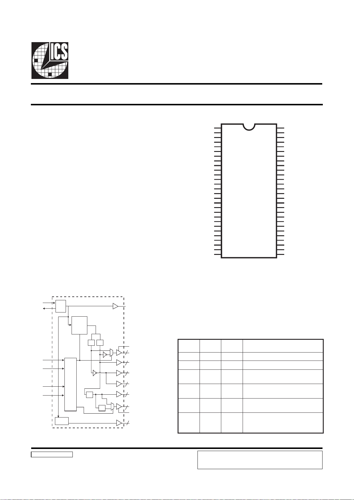
Block Diagram
9250-16 Rev H 9/5/00
Recommended Application:
810/810E type chipset.
Output Features:
• 3 CPU (2.5V) 66.6/133.3MHz (up to 150MHz
achievable through I
2
C)
• 9 SDRAM (3.3V) @ 133.3MHz (up to 150MHz
achievable through I
2
C)
• 8 PCI (3.3 V) @33.3MHz
• 2 IOAPIC (2.5V) @ 33.3MHz
• 2 Hublink clocks (3.3 V) @ 66.6MHz
• 2 USB (3.3V) @ 48MHz ( Non spread spectrum)
• 1 REF (3.3V) @ 14.318MHz
Features:
• Supports spread spectrum modulation,
down spread 0 to -0.5% and ± 0.25% center spread.
•I
2
C support for power management
• Efficient power management scheme through PD#
• Uses external 14.138MHz crystal
• Alternate frequency selections available through I
2
C
control.
Functionality
Pin Configuration
56-Pin 300mil SSOP
* This input has a 50KW pull-down to GND.
*FS2//REF0
VDD0
X1
X2
GND0
GND1
3V66-0
3V66-1
VDD1
VDD2
PCICLK0
PCICLK1
PCICLK2
GND2
PCICLK3
PCICLK4
GND2
PCICLK5
PCICLK6
PCICLK7
VDD2
VDD3
GND3
GND4
48MHz_0
48MHz_1
VDD4
FS0
GNDL1
IOAPIC0
IOAPIC1
VDDL1
CPUCLK0
VDDL0
CPUCLK1
CPUCLK2
GNDL0
GND5
SDRAM0
SDRAM1
VDD5
SDRAM2
SDRAM3
GND5
SDRAM4
SDRAM5
VDD5
SDRAM6
SDRAM7
GND5
SDRAM_F
VDD5
PD#
SCLK
S DATA
FS1
ICS9250-16
1
2
3
4
5
6
7
8
9
10
11
12
13
14
15
16
17
18
19
20
21
22
23
24
25
26
27
28
56
55
54
53
52
51
50
49
48
47
46
45
44
43
42
41
40
39
38
37
36
35
34
33
32
31
30
29
REF0
CPU66/100/133 [2:0]
VDDL
3V66 [1:0]
SDRAM [7:0]
PCICLK [7:0]
IOAPIC [1:0]
VDDL
SDRAM_F
PLL2
48MHz [1:0]
X1
X2
XTAL
OSC
Control
Logic
Config
Reg
FS(2:0)
PD#
2
3
2
8
1
8
2
/2
/2
/3
/2
PLL1
Spread
Spectrum
SDATA
SCLK
Frequency Generator & Integrated Buffers for Celeron & PII/III™
2SF1SF0SFnoitcnuF
X00 etatsirT
X0 1tseT
010
zHM66=UPCevitcA
zHM001=MARDS
011
zHM001=UPCevitcA
zHM001=MARDS
111
zHM331=UPCevitcA
zHM001=MARDS
110
)noitidnoClaicepS(
zHM331=UPCevitcA
zHM331=MARDS
ICS reserves the right to make changes in the device data identified in
this publication without further notice. ICS advises its customers to
obtain the latest version of all device data to verify that any
information being relied upon by the customer is current and accurate.

2
ICS9250-16
The ICS9250-16 is a single chip clock solution for 810/810E type
chipset. It provides all necessary clock signals for such
a system.
Spread spectrum may be enabled through I
2
C programming. Spread
spectrum typically reduces EMI by 8dB to 10 dB. This simplifies
EMI qualification without resorting to board design iterations or
costly shielding. The ICS9250-16 employs a proprietary closed
loop design, which tightly controls the percentage of spreading
over process and temperature variations.
General Description
Pin Configuration
REBMUNNIPEMANNIPEPYTNOITPIRCSED
1
2SFNI
ytilanoitcnuftuptuolla,ycneuqerfUPCsenimreteD.niptceleSnoitcnuF
K05htiw(
W
.)nwod-llup
0FERTUO.tuptuokcolcecnereferzHM813.41,V3.3
31XNI
kcabdeefdna)Fp33(pacdaollanretnisah,tupnilatsyrC
2Xmorfrotsiser
42XTUO
daollanretnisaH.zHM813.41yllanimon,tuptuolatsyrC
)Fp33(pac
,32,71,41,6,5
74,14,53,42
)5:0(DNGRWPylppusV3.3rofsnipdnuorG
7,8]0:1[66V3TUOBUHrofstuptuokcolczHM66dexiFV3.3
,12,01,9,2
44,83,33,72,22
)5:0(DDVRWPylppusrewopV3.3
,61,81,91,02
11,21,31,51
]0:7[KLCICPTUOSKLCUPCsuonorhcnyShtiw,stuptuokcolcICPV3.3
62,52)1:0(zHM84TUOBSUrofstuptuokcolczHM84dexiFV3.3
92,82)1:0(SFNI
.ytilanoitcnuftuptuolla,ycneuqerfUPCsenimreteD.sniptceleSnoitcnuF
.3egapnoelbatytilanoitcnuFotreferesaelP
03ATADSNIIroftupniataD
2
.tupnilairesC
13KLCSNIIfotupnikcolC
2
tupniC
23#DPNI
otniecivedehtnwodrewopotdesuniptupniwolevitcasuonorhcnysA
dnaOCVehtdnadelbasideraskcolclanretniehT.etatsrewopwola
ebtonlliwnwodrewopehtfoycnetalehT.deppotseralatsyrceht
.sm3nahtretaerg
,04,93,73,63
64,54,34,24
]0:7[MARDSTUO
ffodenrutebnacstuptuoMARDSllA.zHM001gninnurtuptuoV3.3
Ihguorht
2
C
43F_MARDSTUOIhguorhtffodenrutebtonnac,MARDSzHM001gninnureerfV3.3
2
C
84,65]0:1[LDNGRWPCIPA&UPCrofylppusrewopV5.2rofdnuorG
25,05,94]0:2[KLCUPCTUO
gnidnepedzHM331rozHM001,zHM66.tuptuokcolcsubtsoHV5.2
.snip)2:0(SFno
35,15)1:0(LDDVRWPCIPAOI&UPCrofylppusrewopV5.2
55,45]0:1[CIPAOITUO.zHM3.33tagninnurstuptuokcolcV5.2
Power Groups
VDD0, GND0 = REF & Crystal
VDD1, GND1 = 3V66 (0:1)
VDD2, GND2 = PCICLK(0:7)
VDD3, GND3 = PLL core
VDD4, GND4 = 48MHz (0:1)
VDD5, GND5 = SDRAM_F, SDRAM (0:7)
VDDL0, GNDL0 = CPUCLK (0:2)
VDDL1, GNDL1 = IOAPIC (0:1)
3
ICS92 50-16
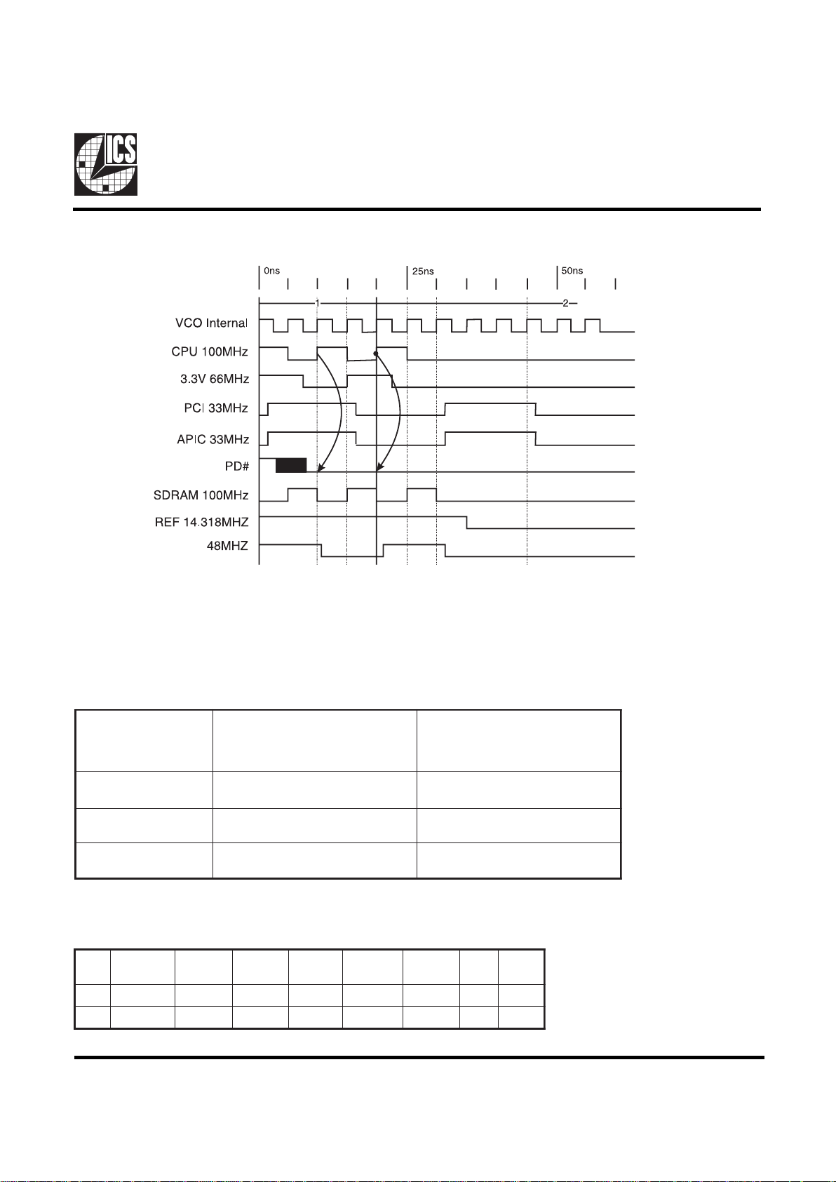
Power Down Waveform
Note
1. After PD# is sampled active (Low) for 2 consective rising edges of CPUCLKs, all
the output clocks are driven Low on their next High to Low tranistiion.
2. Power-up latency <3ms.
3. Waveform shown for 100MHz
Maximum Allowed Current
E018
noitidnoC
noitpmusnocylppusV5.2xaM
,sdaolpacetercsidxaM
V526.2=2qddV
DNGro3qddV=stupnicitatsllA
noitpmusnocylppusV5.2xaM
,sdaolpacetercsidxaM
V564.3=2qddV
DNGro3qddV=stupnicitatsllA
edoMnwodrewoP
0=#NWDRWP(
Am01Am01
zHM66evitcAlluF
01=0,1LES
Am07Am013
zHM001evitcAlluF
11=0,1LES
Am001Am003
Clock Enable Configuration
#DPKLCUPCMARDSCIPAOIzHM66KLCICP
,FER
zHM84
csOsOCV
0WOLWOLWOLWOLWOLWOLFFOFFO
1NONONONONONONONO
4
ICS9250-16
1. The ICS clock generator is a slave/receiver, I2C component. It can read back the data stored in the latches for
verification. Read-Back will support Intel PIIX4 "Block-Read" protocol.
2. The data transfer rate supported by this clock generator is 100K bits/sec or less (standard mode)
3. The input is operating at 3.3V logic levels.
4. The data byte format is 8 bit bytes.
5. To simplify the clock generator I
2
C interface, the protocol is set to use only "Block-Writes" from the controller. The
bytes must be accessed in sequential order from lowest to highest byte with the ability to stop after any complete byte
has been transferred. The Command code and Byte count shown above must be sent, but the data is ignored for those
two bytes. The data is loaded until a Stop sequence is issued.
6. At power-on, all registers are set to a default condition, as shown.
General I2C serial interface information
The information in this section assumes familiarity with I2C programming.
For more information, contact ICS for an I
2
C programming application note.
How to Write:
Controller (host) sends a start bit.
Controller (host) sends the write address D2
(H)
ICS clock will acknowledge
Controller (host) sends a dummy command code
ICS clock will acknowledge
Controller (host) sends a dummy byte count
ICS clock will acknowledge
Controller (host) starts sending first byte (Byte 0)
through byte 5
ICS clock will acknowledge each byte one at a time.
Controller (host) sends a Stop bit
How to Read:
Controller (host) will send start bit.
Controller (host) sends the read address D3
(H)
ICS clock will acknowledge
ICS clock will send the byte count
Controller (host) acknowledges
ICS clock sends first byte (Byte 0) through byte 5
Controller (host) will need to acknowledge each byte
Controller (host) will send a stop bit
Notes:
Controller (Host) ICS (Slave/Receiver)
Start Bit
Address
D3
(H)
AC
K
Byte Count
ACK
Byte
0
ACK
Byte 1
ACK
Byte
2
ACK
Byte
3
ACK
Byte 4
ACK
Byte
5
ACK
Stop Bit
How to Read:
Controller (Host) ICS (Slave/Receiver)
Start Bit
Address
D2
(H)
AC
K
Dummy Command Code
AC
K
Dummy Byte Count
AC
K
Byte 0
AC
K
Byte 1
ACK
Byte 2
AC
K
Byte 3
AC
K
Byte 4
AC
K
Byte 5
AC
K
Stop Bit
How to Write:

5
ICS92 50-16
tiBnoitpitcseDDWP
7tiB )lamronetarepootkcolc0ebotsdeeN(TIBDEVRESERSCI0
6tiB )lamronetarepootkcolc0ebotsdeeN(TIBDEVRESERSCI0
5tiB )lamronetarepootkcolc0ebotsdeeN(TIBDEVRESERSCI0
tiB
)0,3(
)0,3(tiB
KLCUPC
zHM
MARDS
zHM
66V3
zHM
KLCICP
zHM
XXXX
1etoN
2SF
)WH(
0SF
)WH(
1LES
)3tiB(
0LES
)0tiB(
0000 76.6600.00106.6603.33
0001 00.0700.50100.0700.53
0010 76.2700.90176.2733.63
0011 76.4700.21166.4733.73
0100 00.00100.00106.6603.33
0101 00.50100.50100.0700.53
0110 00.90100.90176.2733.63
0111 10.21100.21166.4733.73
1000 43.33143.33166.8833.44
100 1 00.04100.50100.0700.53
10 10 00.02100.0900.0600.03
10 1 1 00.42100.42166.2833.14
1100 43.33100.00106.6603.33
1101 00.05100.05100.5705.73
1110 00.04100.04100.0700.53
1111 99.23199.23106.6603.33
4tiB
%5.-ot0murtcepSdaerpSdaerpSnwoD=0
%52.±murtcepSdaerpSdaerpSretneC=1
0
2tiB)noitarepokcolclamronrof1ebotsdeeN(desutoN 1
1tiB)noitarepokcolclamronrof1ebotsdeeN(desutoN 1
Byte 5: ICS Reserved Functionality and frequency select register (Default as noted in PWD)
Note1: Default at power-up will be for Bit 3 and Bit 0 to be 00, with external hardware selection of FS0, FS2
defining specific frequency.

6
ICS9250-16
Byte 0: Control Register
(1 = enable, 0 = disable)
Byte 1: Control Register
(1 = enable, 0 = disable)
Byte 2: Control Register
(1 = enable, 0 = disable)
Notes:
1. Inactive means outputs are held LOW and are disabled from switching.
These outputs are designed to be configured at power-on and are not
expected to be configured during the normal modes of operation.
2. PWD = Power on Default
tiB#niPemaNDWPnoitpircseD
7tiBDIdevreseR0)evitcanI/evitcA(
6tiBDIdevreseR0)evitcanI/evitcA(
5tiBDIdevreseR0)evitcanI/evitcA(
4tiBDIdevreseR1)evitcanI/evitcA(
3tiB
murtcepSdaerpS
)ffO=0/nO=1(
1)evitcanI/evitcA(
2tiB621zHM841)evitcanI/evitcA(
1tiB520zHM841)evitcanI/evitcA(
0tiB942KLCUPC1)evitcanI/evitcA(
tiB#niPemaNDWPnoitpircseD
7tiB637MARDS1)evitcanI/evitcA(
6tiB736MARDS1)evitcanI/evitcA(
5tiB935MARDS1)evitcanI/evitcA(
4tiB044MARDS1)evitcanI/evitcA(
3tiB243MARDS1)evitcanI/evitcA(
2tiB342MARDS1)evitcanI/evitcA(
1tiB541MARDS1)evitcanI/evitcA(
0tiB640MARDS1)evitcanI/evitcA(
Notes:
1. Do not write in ID bits, these bits are for ICS internal use only.
2. Bit 0 will always read back 0. If readback/rewrite procedure is to
perform, user will need to ensure a "1" is written to Bit 0 for CPUCLK2
to maintain running status.
tiB#niPemaNDWPnoitpircseD
7tiB027KLCICP1)evitcanI/evitcA(
6tiB916KLCICP1)evitcanI/evitcA(
5tiB815KLCICP1)evitcanI/evitcA(
4tiB614KLCICP1)evitcanI/evitcA(
3tiB513KLCICP1)evitcanI/evitcA(
2tiB312KLCICP1)evitcanI/evitcA(
1tiB211KLCICP1)evitcanI/evitcA(
0tiB- devreseR1)evitcanI/evitcA(
 Loading...