

Page 1

S-14425XZ-C1
Jun. 2008
VHF FM REPEATER
Page 2
This service manual describes the latest service information
for the IC-FR5000 IC-FR5100 VHF FM REPEATER at the
time of publication.
NEVER connect the repeater to an AC outlet or to a DC
power supply that uses more than specifed. This will ruin
the repeater.
DO NOT expose the repeater to rain, snow or any liquids.
DO NOT reverse the polarities of the power supply when
connecting the repeater.
DO NOT apply an RF signal of more than 20 dBm (100 mW)
to the antenna connector. This could damage the repeater’s
front-end.
To upgrade quality, any electrical or mechanical parts and
internal circuits are subject to change without notice or
obligation.
MODEL VERSION
CH. SPACING
(kHz)
TX
POWER
FREQUENCY
RANGE
IC-FR5000
USA-01 7.5/15/30
50 W
136–174 MHzEXP-01 12.5/25.0
IC-FR5100 EUR-01 12.5/20.0/25.0 25 W
Be sure to include the following four points when ordering
replacement parts:
1. 10-digit Icom parts numbers
2. Component name
3. Equipment model name and unit name
4. Quantity required
<ORDER EXAMPLE>
1110003491 S.IC TA31136FNG IC-FR5000 MAIN UNIT 5 pieces
8820001210 Screw 2438 screw IC-FR5000 Top cover 10 pieces
Addresses are provided on the inside back cover for your
convenience.
Icom, Icom Inc. and
logo are registered trademarks of Icom Incorporated (Japan) in the United States, the United
Kingdom, Germany, France, Spain, Russia and/or other countries.
ORDERING PARTS
1. Make sure the problem is internal before disassembling
the repeater.
2. DO NOT open the repeater until the repeater is
disconnected from its power source.
3. DO NOT force any of the variable components. Turn
them slowly and smoothly.
4. DO NOT short any circuits or electronic parts. An
insulated tuning tool MUST be used for all adjustments.
5. DO NOT keep power ON for a long time when the
repeater is defective.
6. DO NOT transmit power into a Standard Signal
Generator or a Sweep Generator.
7. ALWAYS connect a 50 dB to 60 dB attenuator between
the repeater and a Deviation Meter or Spectrum
Analyzer when using such test equipment.
8. READ the instructions of test equipment throughly
before connecting a test equipment to the repeater.
REPAIR NOTES
INTRODUCTION CAUTION
UNIT ABBREVIATIONS:
F=FRONT UNIT
M=MAIN UNIT
CN=CONNECT UNIT
Page 3

CONTENTS
SECTION 1 SPECIFICATIONS
SECTION 2 INSIDE VIEWS
SECTION 3 DISASSEMBLY INSTRUCTION
SECTION 4 OPTIONAL UNIT INSTALLATION
SECTION 5 CIRCUIT DESCRIPITON
5-1 RECEIVER CIRCUITS. . . . . . . . . . . . . . . . . . . . . . . . . . . . . . . . . . . . . . . . . . . . . . . . . . . . . . . . 5-1
5-2 TRANSMITTER CIRCUITS . . . . . . . . . . . . . . . . . . . . . . . . . . . . . . . . . . . . . . . . . . . . . . . . . . . . 5-1
5-3 OTHER CIRCUITS . . . . . . . . . . . . . . . . . . . . . . . . . . . . . . . . . . . . . . . . . . . . . . . . . . . . . . . . . . 5-2
5-4 CPU (M: IC20) PORT ALLOCATION. . . . . . . . . . . . . . . . . . . . . . . . . . . . . . . . . . . . . . . . . . . . . 5-3
SECTION 6 ADJUSTMENT PROCEDURES
6-1 PREPARATION . . . . . . . . . . . . . . . . . . . . . . . . . . . . . . . . . . . . . . . . . . . . . . . . . . . . . . . . . . . . . 6-1
6-2 FREQUENCY ADJUSTMENT. . . . . . . . . . . . . . . . . . . . . . . . . . . . . . . . . . . . . . . . . . . . . . . . . . 6-6
6-3 TRANSMIT ADJUSTMENT . . . . . . . . . . . . . . . . . . . . . . . . . . . . . . . . . . . . . . . . . . . . . . . . . . . . 6-7
6-4 RECEIVE ADJUSTMENT . . . . . . . . . . . . . . . . . . . . . . . . . . . . . . . . . . . . . . . . . . . . . . . . . . . . . 6-8
SECTION 7 PARTS LIST
SECTION 8 MECHANICAL PARTS
SECTION 9 BOARD LAYOUTS
SECTION 10 BLOCK DIAGRAM
SECTION 11 VOLTAGE DIAGRAM
FRONT UNIT . . . . . . . . . . . . . . . . . . . . . . . . . . . . . . . . . . . . . . . . . . . . . . . . . . . . . . . . . . . . . . 11-1
MAIN UNIT (1/3) . . . . . . . . . . . . . . . . . . . . . . . . . . . . . . . . . . . . . . . . . . . . . . . . . . . . . . . . . . . . 11-2
MAIN UNIT (2/3) . . . . . . . . . . . . . . . . . . . . . . . . . . . . . . . . . . . . . . . . . . . . . . . . . . . . . . . . . . . . 11-3
MAIN UNIT (3/3) . . . . . . . . . . . . . . . . . . . . . . . . . . . . . . . . . . . . . . . . . . . . . . . . . . . . . . . . . . . . 11-4
CONNECT UNIT . . . . . . . . . . . . . . . . . . . . . . . . . . . . . . . . . . . . . . . . . . . . . . . . . . . . . . . . . . . . 11-5
Page 4
1 - 1
SECTION 1 SPECIFICATIONS
M GENERAL
[FR5000] [FR5100]
• Frequency coverage 136–174 MHz
• Conventional channels max. 32 ch
• Type of emission Wide
16K0F3E
Middle – 14K0F3E
Narrow
11K0F3E/11K0F7E/11K0F7D/11K0F7W
/
8K50F3E ([EXP-01] only)
8K50F3E
Digital 4K00F1E/4K00F1D/4K00F3E
• Antenna impedance 50 Ω (Nominal)
• Operating temperature range –22˚F to +140˚F (–30˚C to +60˚C) –25˚C to +55˚C
• Power supply requirement
(nominal)
13.6 V DC (Negative ground) 13.2 V DC (Negative ground)
• Current drain (Approx.) Receiving 500 mA (stand-by), 1900 mA (max. audio)
Transmitting 15 A (at 50 W) 8.0 A (at 25 W)
• Dimensions
(Projections not included)
19 (W)×3
15
⁄32 (H)×10 1⁄4 (D) in. 483 (W)×88 (H)×260 (D) mm
• Weight (Approx.) 12 Ib 5
17
/32 oz. 5.6 kg
M TRANSMITTER
[FR5000] [FR5100]
• Output power 50 W 25 W
• Modulation Variable reactance frequency modulation
• Max. frequency deviation Wide ±5.0 kHz
Middle – ±4.0 kHz
Narrow ±2.5 kHz
• Frequency stability ±0.5 ppm ±0.2 kHz
• Spurious emissions 80 dB typ. 0.25 μW (≤1 GHz), 1.00 μW (>1 GHz)
• Adjacent channel power Wide 76 dB typ. 76 dB typ.
Middle – 76 dB typ.
Narrow 69 dB typ. 70 dB typ.
Digital 65 dB typ. 66 dB typ.
• Audio harmonic distortion 1% typ. (at AF 1 kHz 40% deviation)
• Intermodulation attenuation – 40 dB min.
• Audio frequency response +2 dB to –8 dB of 6 dB/oct. Wide/Middle from 300 Hz to 3000 Hz
Narrow from 300 Hz to 2550 Hz
• FM Hum and noise
(300 Hz–3000 Hz, 750 µs)
Wide 52 dB typ.
–
Narrow 49 dB typ.
• Audio input impedance (Microphone) 600
Ω
Page 5
1 - 2
M RECEIVER
[FR5000] [FR5100]
• Receive system Double-conversion superheterodyne system
• Intermediate frequencies 1st IF: 46.35 MHz, 2nd IF: 450 kHz
• Sensitivity Wide/Narrow 0.3 μV typ. at 12 dB SINAD –10 dBμV max. at 12 dB SINAD
Wide/Middle/Narrow – –10 dBμV max. at 12 dB SINAD
Digital 0.25 μV typ. at 5% BER 0 dBμV emf max. at 1% BER (PN9)
• Squelch sensitivity (at threshold) 0.25 μV typ.
• Adjacent channel selectivity Wide 80 dB typ. (TIA-603-B)
85 dB typ. (TIA-603)
86 dB typ.
Middle – 83 dB typ.
Narrow 56 dB typ. (TIA-603-B)
77 dB typ. (TIA-603)
77 dB typ.
Digital 66 dB typ. (EN 301 166, 400 Hz @1%)
63 dB typ. (EN 301 166, PN15 @5%)
67 dB typ.
• Spurious response Analog 90 dB 80 dB typ.
Digital 90 dBµV emf 90 dBµ Vemf typ.
• Intermodulation Wide 78 dB typ. 72 dB typ.
Middle – 72 dB typ.
Narrow 78 dB typ. 71 dB typ.
Digital 75 dBµV emf typ. 76 dBµV emf typ.
• Hum and noise Wide 52 dB typ. –
Middle – –
Narrow 50 dB typ. –
Digital 66 dB typ. –
• Audio output power
(at 5% distortion with a 4 Ω load)
4.0 W typ. 3.5 W min.
• Audio output impedance 4
Ω
Specifications are measured in accordance with TIA–603–B (for Wide and Narrow) or EN 300 166 (Digital) for FR5000.
Specifications are measured in accordance with EN 300 086 (for Wide, Middle and Narrow) or EN 301 166 (Digital) for FR5100.
All stated specifications are subject to change without notice or obligation.
Page 6
2 - 1
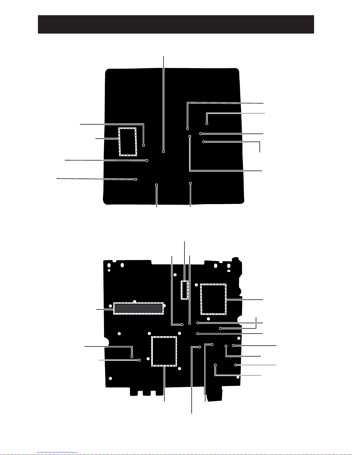
SECTION 2 INSIDE VIEWS
RX VCOs
• MAIN UNIT
(TOP VIEW)
• MAIN UNIT
(BOTTOM VIEW)
Power SW (VCC line)
(Q57)
8V regulator (8V line)
(IC27)
AF AMP
(IC34)
FUNCTION
(Ref.No.)
2nd IF filter (Wide)
(FI1)
2nd IF filter (Narrow)
(FI2)
CPU
(IC20)
5V regulator (DSP5V line)
(IC39)
CPU clock
(X5)
PLL IC (TX lopp)
(IC3)
TX VCOs
Optional digital unit slot
TX power AMP
(IC22)
1st mixer (DBM)
(D62, L27, 32)
5V regulator (CPU5V)
(IC30)
5V regulator (+5V line)
(Q41)
EEPROM
(IC21)
DSP
(IC12)
AF SW
(IC35)
PLL IC (RX loop)
(IC4)
Ref. OSC
(X1)
Level converter
(IC26)
8V regulator (T8V line)
(Q45)
D/A converter
(IC20)
Discriminator
(X3)
IF IC
(IC5)
FUNCTION
(IC40)
Liner codec
(IC8)
Page 7

2 - 2
• FRONT UNIT
FRONT CPU
(IC503)
CLOCK OSC
(X501)
LCD DRIVER
(IC500)
ANALOG SW
(IC506)
AF POWER AMP.
(IC509)
SPEAKER SW
(Q508)
Page 8
3 - 1
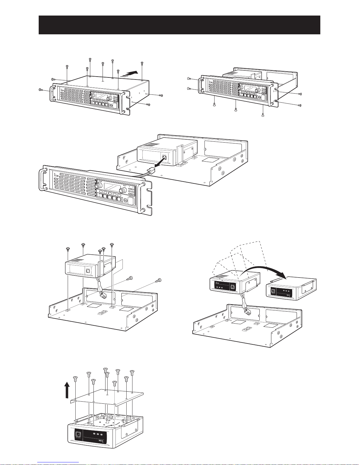
SECTION 3 DISASSEMBLY INSTRUCTION
1. Removing the front panel
q Unscrew 11 screws from the top cover.
3. Removing the MAIN UNIT
q Unscrew 9 screws, and remove the cover.
(If you are going to install an optional unit, see page 4-1 for the installation.)
2. Removing the MAIN UNIT assembly
q Uscrew 5 screws which settles the MAIN UNIT assembly.
P
0
P
1
P
2
P
3
P
4
P
0
P
1
P
2
P
3
P
4
P
0
P
1
P
2
P
3
P
4
PWR TX RX
PWR
TX RX
PWR TX RX
w Unscrew 7 screws from the front panel.
e Disconnect the cable from the MAIN UNIT assembly, and remove the front panel.
w Turn the MAIN UNIT assembly upside down.
(To be continued to next page)
Page 9
3 - 2
MAIN
MAIN
J9J9J9
J4
J4
Unscrew
ANT case
Unsolder
ANT case
Flat cable
Disconnect
Disconnect
Black
Black
Black
Black
Red
Red
Red
Red
W4
W4
Unsolder 2 points
Unsolder 4 points
Unscrew
Clip
15 screws
w Unsolder 2 points at the ANT cases.
e Unscrew 4 screws from the ANT cases,
and remove them.
r Disconnect the flat cabe from J4 and the
speaker cable from J9.
t Unsolder 2 points at the bottom of ANT connectors.
y Unsolder 4 points at the PA module leads.
u Unscrew 2 screws from W4.
i Remove the clip from the side of chassis.
o Unscrew 15 screws from the MAIN UNIT, then take off
the MAIN UNIT PCB from the chassis.
Page 10
4 - 1
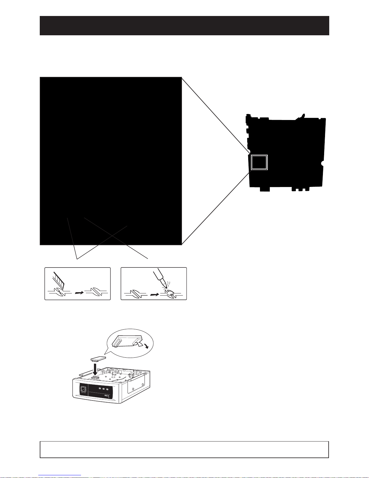
SECTION 4 OPTIONAL UNIT INSTALLATION
PWR TX RX
q Disassembly the repeater until the MAIN UNIT is exposed. (See the page 3-1)
w Modify the patter ns on the MAIN UNIT as below.
e Remove the protective paper of optional unit, and install it to the J1 as below.
A and F; Cut the pattern
B; Short the pattern
r Replace the cover, screws, etc. to recover the whole assembly.
NOTE: When uninstalling the scrambler unit
Be sure to recover the disconnected or connected points, otherwise no TX modulation or AF output is available.
Install UT-109R or UT-110R as follows.
<MAIN UNIT (bottom side)>
Page 11

5 - 1
SECTION 5 CIRCUIT DESCRIPTION
5-1 RECEIVER CIRCUITS
RF BPF CIRCUITS
RX signals from the RX antenna connector (J11) are passed
through the 1st stage of BPF (D28, 29, 31, 32, L44, 47) then
amplified by the RF AMP (Q36). The amplified RX signals
are passed through the 2nd stage of BPF (D28, 29, 31,
32, L44, 47) to remove unwanted signals for good image
response then applied to the 1st mixer (L27, 32, D62).
Being mixed with 1st LO signals from the RX VCO, the RX
signals are converted into the 46.35 MHz 1st IF signal.
The 1st and 2nd stage of the BPFs are tuned to the pass
band frequency by tracking voltage “T1” and “T2” from
the DAC (IC17). The gain of low noise RF AMP (Q36) is
controlled by the AGC circuit (Q39, D27) according to the
RX signal strength.
IF FILTER/IF AMP CIRCUITS
The 1st IF signal from the 1st mixer (L27, 32, D62) is
amplifi ed by the buffer AMP (Q63, 64, 71) and 1st stage of
IF AMP (Q19) then fi ltered by crystal fi lter (FI3 or FI4), and
then applied to the IF IC (IC5).
The crystal fi lters (FI3 or FI4) are switched by the “NWC1”
signal from the CPU (IC20) according to the RX mode; Wide
(Middle), Narrow or Digital.
<ANALOG RX>
Being mixed with the 2nd LO, the 1st IF signal is converted
into the 450 kHz 2nd IF signal. The 2nd IF signal is passed
through the external ceramic filter (FI1 or FI2), then FMdemodulated by the internal quadrature detector with
discriminator (X3). The demodulated AF signals are
amplifi ed by the AF AMP (IC36), and applied to the LINER
CODEC (IC8). The AF signals are converted into the
digital audio signal then processed by the DSP (IC12) then
recovered to the analog audio signals.
The ceramic filter (FI1 or FI2) is switched by the “NWC2”
signal from the CPU (IC20) according to the RX mode; Wide
(Middle), Narrow or Digital.
<DIGITAL RX>
The 450 kHz 2nd IF signal is amplifi ed by IC7 then applied
to the DSP (IC12) via ADC (IC9), and digital-demodulated.
The processed digital signal is converted into the analog
audio signal by the LINEAR CODEC (IC8).
AF AMPLIFIER CIRCUITS
The AF signals from the LINEAR CODEC are amplifi ed by
the AF AMP (IC36) and level-adjusted by DAC (IC2), then
applied to IC28 via IC29 to be power-amplifi ed.
SIGNALING (DECODE)
The Continious Tone (CTCSS/DTCS), Single Tone (5-Tone/
DTMF/CW_ID) signals in the demodulated AF signals are
decoded in the DSP (IC8).
5-2 TRANSMITTER CIRCUITS
MODULATION CIRCUITS
The demodulated signals are applied to the MIC AMP (IC25).
The amplified Demodulated signals are passed through the
SW IC (IC35) which selects the source of Demodulated signals
from J5 (from MIC) and from D-SUB connector (DEXM).
The Demodulated signals from the SW IC are amplifi ed by
an AMP (IC1) then applied to the LINEAR CODEC IC (IC8)
where the Demodulated signals are converted in to the
digital audio signals.
The converted digital audio signals are processed (preemphasis, limit, etc.) by the DSP (IC12), then recovered to
the analog audio signals by LINER CODEC IC (IC8). The AF
signals are amplifi ed by IC1 and level-adjusted by Electronic
VR (IC2), then applied to the TX VCO and TCXO (X1) as the
modulation signals.
SIGNALING (ENCODE)
The Continious Tone (CTCSS/DTCS), Single Tone (5-Tone/
DTMF/CW_ID) signals are encoded, and mixed with
Demodulated signals in the DSP (IC12).
YGR/PA CIRCUITS
The output signals from TX VCOs are amplified to the level
required for the PA module by pre-AMPs (Q37, 38), then
amplifi ed b y the PA module (IC22) to obtain TX output power. The
power-amplifi ed TX signal is passed through the ANT SW (D44)
and LPF (for harmonics removal) then applied to the TX antenna.
APC CIRCUIT
D45, D48 and D49 detect the TX power, and the detected
voltage is applied to the IC23 in APC circuit. Comparing the
detected voltage which is in proportion to the TX power and
power setting voltage as the reference voltage, IC23 adjusts
the bias voltage of PA module (pin 2: VGG terminal) and preAMP (Q38) to control the TX power.
Page 12

5 - 2
5-3 FREQUENCY SYNTHESIZER CIRCUITS
RX PLL CIRCUIT
The RX PLL IC (IC4) outputs resulting signal; phase-comparison
of reference signal (15.3 MHz) from the TCXO (X2) and fedback
OSC signal from the RX VCO. The phase-difference signal is
passed through the active loop fi lter (Q11, 14) and applied to the
RX VCO as the lock voltage. The voltage of RX LV (lock voltage)
is adjusted to appropriate one by “RX LVA” signal.
A portion of reference frequency signal (15.3 MHz) from the
TCXO (X2) is passed through the tripler (Q2) to extract 3rd
harmonic, then applied to the IF IC (IC5).
RX VCO
There are 2 VCOs; VCO for lower band (Q21, D8, 16, L17) and
higher band (Q20, D7, 15, L20), and these VCOs (=OSC freq.)
are switched by the VCO SW (Q26, 30). The OSC frequencies
of these VCOs are adjusted (=Locked) to desired one by the
RX LV signal (Lock Voltage). The output signals of these VCOs
are applied to the 1st mixer (L27, 32, D62) via buffer (Q25).
A portion of output signal from the buffer (Q25) is applied to
the doubler (Q32) to extract 2nd harmonic, then applied to
the PLL IC (IC4) via the LPF.
TX PLL CIRCUIT
TX PLL IC (IC3) outputs resulting signal; phase-comparison
of reference signal (15.3 MHz) from the TCXO (X1) and
fedback OSC signal from the TX VCO. The phase-difference
signal from the PLL IC (IC3) is passed through the active
loop fi lter (Q10, 13) and applied to the TX VCO as the lock
voltage. The rock voltage “TX LV” is adjusted to appropriate
one by the LVA signal. The OSC signal of TCXO (X1) is FMmodulated by applied modulation signals.
TX VCO CIRCUITS
There are 2 VCOs; VCO for lower band (Q23, D10, 14, L62)
and higher band (Q22, D9, 13, L14), and these VCOs (=OSC
frequencies) are switched by the VCO SW (Q27, 28). The
OSC frequencies of these VCO are adjusted (=Locked) to
desired one by the TX LV signal (Lock Voltage).
The modulation signals applied to the Var iable Capacitor
(VD; D18 or D30) vary the capacitor reactance of it for FM
modulation. The output signals of these VCOs are applied to
the YGR/PA circuits via buffers (Q24, 35).
A portion of these output signal is passed through the
doubler (Q33) to extract 2nd harmonic, then applied to the
PLL IC (IC3) via the LPF.
5-4 OTHER CIRCUITS
POWER SUPPLY
The power supply is switched by Q57 (ON/OFF). 5V (REF5)
from the regulator (IC30) is passed through L58 to supply to
CPU. The 5V also supplies to other sections of the repeater
via Q41 as “+5V.”
8V from the regulator (IC27) are supplies to various circuits,
and also supplies to TX circuits as “T8V” and RX circuits as
“8V.”
5V from the regulator (IC39) supplies DSP as “DSP5” and
supplies logic circuits; CPU, DSP, etc. via regulators (IC13,
14, 15).
The regulator “F8V” (IC41) provides the supply for FRONT
UNIT.
COMPANDER
The compander in the DSP (IC12) compresses the
amplitude of Demodulated signals in TX, and expands in RX
to provide high quality, high S/N ratio recovered sounds.
LEDs
DS1 (BUSY), DS2(PWR) and DS3 (TX) indicate the
repeater’s status: Power ON, T/RX and Cloning.
Page 13

5 - 3
Pin
No.
LINE NAME DESCRIPTION
IN/
OUT
CONDITION
1–11 D5–D15 DSP data bus line. I/O –
15–28 A1–A14 DSP data bus line. I/O –
29 HRW DSP data line. I/O –
32 FANS Cooling fan (CH: MF1) rotation detect. I "H"=While the cooling fan is rotating.
33 TLED TX indicator LED control signal. O "H"=TX
34 LEDR RX indicator LED control signal. O "H"=Squelch open.
35 PLSCK PLL (M: IC4) serial clock. O –
36 PLSSO PLL (M:IC4) serial data. O –
41 PWON Power line "VCC" control signal. O "H"=Power ON.
42 AFON2 AF power AMP. (M: IC28) control signal. O "H"=AF power AMP ON.
43 AFON AF output select signal. O
"H= AF signals are output from the
[ACCESSORY CONNECTOR].
44 ESCL Serial clock to the EEPROM (M: IC21). O –
45 ESDA Serial data to the EEPROM (M: IC21). O –
46 TXC TX power line "T8V" control signal. O "H"=TX
47 RXC RX power line "R8V" control signal. O "H"=RX
48 RPLST RX PLL (M: IC4) strobe. O –
49 TPLST TX PLL (M: IC3) strobe. O –
50 RUNLK RX PLL (M: IC4) unlock signal. I "L"=Unlocked
51 TUNLK TX PLL (M: IC3) unlock signal. I "L"=Unlocked
52 XCTS Serial data from the RS-232 line driver (M: IC26). I –
53 XRTS Serial data to the RS-232 line driver (M: IC26). O –
55 EXDA External D/A port. O –
56 BEEP Beep sounds (square waves). O –
57–59 OPV3–OPV1 Optional unit detect. I –
60 MMUT MIC mute signal to the installed optional unit. O "H"=MIC mute
61 HANG Microphone hang-up detect. I "L"=Hang-up
62 PTT [PTT] key input. (pull up) I –
63 RMUT RX mute signal to the installed optional unit. O "H"=RX mute
64 EXAD External A/D port. I –
65 TEMP Temperature detect. I –
68 RLVIN RX PLL lock voltage. I –
69 BATV Voltage monitor (divided voltage of "VCC"). I –
70 TLVIN TX PLL lock voltage. I –
71 RSSI RSSI signal from the IF IC (M: 5). I –
74 XTXD External data to the RS-232 driver (M: IC26). O –
75 XRXD External data from the RS-232 driver (M: IC26). I –
76 TMUT TX mute signal. O "H"=TX mute
77 HINT DSP IC control signal. O –
78 INT1 DSP IC control signal. O –
79 HRDY DSP IC control signal. O –
81 HDS1 DSP IC control signal. O –
82 HDS2 DSP IC control signal. O –
100 RES CPU reset signal from the reset IC (F: IC501). O –
101–108 EXIO1–EXIO8 External data bus line. I/O +5 V pull-up
112 POSW [PWR] key input. (pull-up) I –
113 NOIS Noise detect. I "H"=RX signal is absent (squelch close).
114 CSFT Clock frequency shift signal. O –
119 SSO Serial data to the seri-para converter (M: IC31). O –
120 SCK Clock signal to the seri-para converter (M: IC31). O –
121 EXIO9 External data bus line. I/O +5 V pull-up
122 DSDA Serial data to the DAC (M: IC17). O –
5-5 CPU (M: IC20) PORT ALLOCATION
Page 14

5 - 4
Pin
No.
LINE NAME DESCRIPTION
IN/
OUT
CONDITION
123 DAST Strobe to the DAC (M: IC2). O –
125 FMDA Data from the FRONT CPU (F: IC502). I –
126 MFDA Data to the FRONT CPU (F: IC502). O –
127 OPT2 Port for optional unit. O –
128 OPT1 Port for optional unit. I –
129 OPT3 Port for optional unit. I –
131 CSO Port for optional unit. O –
132 CSI Port for optional unit. I –
133 EXOE Output enable signal to the seri-para converter (M: IC31). O –
134 EXST Strobe to the seri-para converter (M: IC31). O –
135 DRES Reset signal to the DSP IC (M: IC12). O –
136 HCS DSP data line. I/O –
138 GPIO2 DSP data line. I/O –
139 GPIO1 DSP data line. I/O –
140–144 D0–D4 DSP data bus line. I/O –
5-5 CPU (M: IC20) PORT ALLOCATION (continued)
Page 15

6 - 1
SECTION 6 ADJUSTMENT PROCEDURE
6-1 PREPARATION
¤ REQUIRED EQUIPMENTS
EQUIPMENT
SPECIFICATION
EQUIPMENT SPECIFICATION
Adjustment
Software
"CS-FR5000" (Revision 1.0 or later) JIG cable
Modifi ed OPC-1122U (USB type)
(see the illust below)
Power Supply
Output voltage :
13.6 V DC
[FR5000]
13.2 V DC
[FR5100]
Current capacity : More than 20 A
[FR5000]
More than 10 A
[FR5100]
Attenuator
Power attenuation : 40 dB
Capacity : More than 60 W
[FR5000]
More than 30 W
[FR5100]
RF Power Meter
(terminated type)
Measuring range :
1–60 W
[FR5000]
1–30 W
[FR5100]
Frequency range : 100–300 MHz
Impedance : 50
Ω
SWR : Less than 1.2 : 1
Standard Signal
Generator (SSG)
Frequency range : 0.1–300 MHz
Output level : 0.1 mV to 32 mV
(–127 to –17 dBm)
Audio Generator
Frequency range : 300–3000 Hz
Output level : 1–500 mV
Frequency Counter
Frequency range : 0.1–300 MHz
Frequency accuracy
: ±1 ppm or better
Input level : Less than 1 mW
AC Millivoltmeter Measuring range : 10 mV to 10 V
Oscilloscope
Frequency range : DC–20 MHz
Measuring range : 0.01–20 V
Modulation
Analyzer
Frequency range : 30–300 MHz
Measuring range : 0 to ±10 kHz
External Speaker
Input impedance : 4
Ω
Capacity : More than 5 W
¤ JIG CABLE
Add a jumper wire here
OPC-1122U
(USB type Cloning cable)
+
GND
MIC
PTT
GND
PTT
4.7 µF
+−
AC MILLIVOLT METER
(10 mV to 10 V)
AUDIO GENERATOR
(300–3000 Hz/1–100 mV)
+−
GND
SP
+−
EXT. SPEAKER
(5 W/4 Ω)
Page 16

6 - 2
¤ CONNECTION
(Loose Coupling)
FREQUENCY COUNTER
(0.1–300 MHz)
MODULATION ANALYZER
(0.1–300 MHz)
STANDARD SIGNAL GENERATOR
(0.1–300 MHz)
OSCILLOSCOPE
(DC to 10 kHz)
ATTENUATOR
(30 dB/60 W)
RF POWER METER
Black
Red
20 A
fuses
DC power supply
DC power cable
<Rear view>
(Detect output)
Page 17

¤ ADJUSTMENT CHANNEL LISTS
Clone the adjust channels into the repeater before starting adjustment. Each channel must be assigned [Frequency], [RF
PWR], [CH Type], [TX C. Tone] and [W/N] as below.
• Channel list
6 - 3
Page 18

6 - 4
¤ WHOLE PROCEDURE OF THE ADJUSTMENT
q Connect the repeater and PC with the JIG cable (see the page 6-2).
w
Tur n the repeater power ON.
e
Boot up 'CS-FR5000.'
r
Set the [Digital Function] to "Enable."
y Set or modify adjustment values as specifi ed in the guidances on the pages 6-6 to 6-9.
t
Click or [Read <– TR] in the [Adjust] menu, then the "Adjust Utility" window (see the page 6-5) appears.
*For [FR5100]:
Set the [Wide Band Width] to "Middle" when adjust "ANALOG DEVIATION" in Middle mode.
Page 19

Mode setting
TX output power
Analog deviation
Digital deviation
Receive sensitivity (Band center)
Receive sensitivity (Band high)
CTCSS/DTCS deviation
Squelch
TX frequency
Lock volatge
(Preset)
Lock volatge
(Adjustment)
S-meter
Modulation balance
Modulation balance (High)
¤ ADJUST UTILITY WINDOW
6 - 5
Page 20

6-2 FREQUENCY ADJUSTMENT
1) Select an adjustment item using cursor or [↑] / [↓] keys of the PC’s keyboard.
2) Set or modify the adjustment value as specifi ed using [←] / [→] keys of the PC’s keyboard, then push the [ENTER] ke y.
ADJUSTMENT ADJUSTMENT CONDITION OPERATION
ADJUSTMENT
ITEM
VALUE
PLL LOCK
VOLTAGE
-Preparation-
1
–
1) Connect an RF power meter to the
TX antenna.
2) Set the preset adjustment value on
the adjustment utility window.
[LV (RX L)] 161 [3.15V]
[LV (RX H)] 153 [3.00V]
[LV (TX L)] 51 [1.0V]
[LV (TX H)] 36 [0.7V]
-AdjustRX
(Band center)
2 • CH. : 1-1
• Receiving
• Select the item [RX LVA L], then
push the [ENTER] key. [RX LVA L]
(Automatic
adjustment)
RX
(Band high)
3 • CH. : 1-2
• Receiving
•
Select the item [RX LVA H], then
push the [ENTER] key.
[RX LVA H]
TX
(Band low)
4 • CH. : 1-3
• T r ansmitting
• Select the item [TX LVA L], then push
the [ENTER] key.
[TX LVA L]
TX
(Band center)
5 • CH. : 1-4
• T r ansmitting
• Select the item [TX LVA H], then
push the [ENTER] key.
[TX LVA H]
LOCK
VOLTAGE
VERIFY
RX
(Band low)
1 • CH. : 1-5
• Receiving
• Verify the lock voltage at each
channels on the [RX LIVIN] item on
the "I/O Check window" as below.
[RX LIVIN]
(I/O Check
window)
0.5–1.5 V
(Verify)
RX
(Band center)
2 • CH. : 1-6
• Receiving
TX
(Band center)
3 • CH. : 1-7
• T r ansmitting
• Verify the lock voltage at each
channels on the [TX LIVIN] item on
the "I/O Check window" as below.
[TX LIVIN]
(I/O Check
window)
3.0–4.5 V
(Verify)
TX
(Band high)
4 • CH. : 1-8
• T r ansmitting
2.0–3.5 V
(Verify)
TX
FREQUENCY
1
–
1) Set the item [TX Mode] to "1."
2) Connect an RF power meter to the
TX antenna.
[TX Mode]
"1"
2 • CH. : 1-9
• T r ansmitting
1) Adjust the frequency using [←] / [→]
keys of the PC’s keyboard.
2) Push the [ENTER] key to store the
adjust value.
[TX REF]
173.9000 MHz
6 - 6
• I/O CHECK WINDOW
*The above voltages are just an example.
Lock voltage verify
Page 21

6-3 TRANSMIT ADJUSTMENT
1) Select an adjustment item using cursor or [↑] / [↓] keys of the PC’s keyboard.
2) Set or modify the adjustment value as specifi ed using [←] / [→] keys of the PC’s keyboard, then push the [ENTER] ke y.
ADJUSTMENT ADJUSTMENT CONDITION OPERATION
ADJUSTMENT
ITEM
VALUE
TX
Output Power
-Preparation-
1
–
• Connect an RF power meter to the
TX antenna connector.
––
-Adjust(Hi Power)
2 • CH. : 1-10
• T r ansmitting
1)
Adjust the TX output power using [←]
/ [→] keys of the PC’s keyboard.
2) Push the [ENTER] key to store the
adjust value.
[Power(Hi)]
50 W
[FR5000]
25 W
[FR5100]
(L2 Power) 3 • CH. : 1-11
• T r ansmitting
[Power(L2)]
25 W
[FR5000]
10 W
[FR5100]
(L1 Power) 4 • CH. : 1-12
• T r ansmitting
[Power(L1)]
5 W
[FR5000]
2.5 W
[FR5100]
MODULATION
BALANCE
-Preparation-
1• Connect a Modulation Analyzer
to the TX antenna connector
through an attenuator.
• Set the Modulation Analyzer as;
HPF : OFF
LPF : 20 kHz
De-emphasis : OFF
Detector : (P-P)/2
––
2 – • Set the item [TX Mode] to "2." [TX Mode]
"2"
-Adjust(TX VCO 1)
3 • CH. : 1-13
• T r ansmitting
1) Adjust the wave form using [←] / [→]
keys of the PC’s keyboard.
2) Push the [ENTER] key to store the
adjust value.
[BAL]
(square wave
form)
(TX VCO 2) 4 • CH. : 1-14
• T r ansmitting
[BAL Offset
(High]
DIGITAL
DEVIATION
-Preparation-
1 – • Set the item [TX Mode] to "16." [TX Mode]
"16"
2• Connect a Modulation Analyzer
to the TX antenna connector
through an attenuator.
• Set the Modulation Analyzer as;
HPF : OFF
LPF : 20 kHz
De-emphasis : OFF
Detector : (P-P)/2
––
-Adjust(Band 1)
3 • CH. : 1-15
• T r ansmitting
1) Adjust the deviation using [←] / [→]
keys of the PC’s keyboard.
2) Push the [ENTER] key to store the
adjust value.
[MOD (Digital)]
±1.39–1.43
kHz
(Band 2) 4 • CH. : 1-16
• T r ansmitting
[MOD Slant
Band 0]
(Band 3) 5 • CH. : 1-17
• T r ansmitting
[MOD Slant
Band 1]
(Band 4) 6 • CH. : 1-18
• T r ansmitting
[MOD Slant
Band 2]
(Band 5) 7 • CH. : 1-19
• T r ansmitting
[MOD Offset
(High)]
(Band 6) 8 • CH. : 1-20
• T r ansmitting
[MOD Slant
Band 3]
(Band 7) 9 • CH. : 1-21
• T r ansmitting
[MOD Slant
Band 4]
(Band 8) 10 • CH. : 1-22
• T r ansmitting
[MOD Slant
Band 5]
6 - 7
Page 22

6-3 TRANSMIT ADJUSTMENT (continued)
1) Select an adjustment item using cursor or [↑] / [↓] keys of the PC’s keyboard.
2) Set or modify the adjustment value as specifi ed using [←] / [→] keys of the PC’s keyboard, then push the [ENTER] ke y.
ADJUSTMENT ADJUSTMENT CONDITION OPERATION
ADJUSTMENT
ITEM
VALUE
ANALOG
DEVIATION
-Preparation-
1 – • Set the item [TX Mode] to "1." [TX Mode]
"1"
2• Connect a Modulation Analyzer
to the TX antenna connector
through an attenuator.
• Set the Modulation Analyzer as;
HPF : OFF
LPF : 20 kHz
De-emphasis : OFF
Detector : (P-P)/2
––
3• Connect an Audio Generator
to the MIC line through the JIG
cable.
• Set the Audio Generator as;
Modulation : 1050 Hz
Level : 40 mVrms
Waveform : Sine wave
––
-Adjust(Wide)
4 • CH. : 1-23
• T r ansmitting
1) Adjust the deviation using [←] / [→]
keys of the PC’s keyboard.
2) Push the [ENTER] key to store the
adjust value.
[MOD (Wide)]
±4.05–4.15
kHz
(Middle)
<[FR5100] only>
5 • CH. : 1-24
• [Wide Band Width]
: "Middle" (see the page 6-4)
• T r ansmitting
[MOD (Middle)]
±3.15–3.25
kHz
(Narrow) 6 • CH. : 1-25
• T r ansmitting
[MOD (Narrow)]
±2.05–2.15
kHz
CTCSS/DTCS
DEVIATION
-Preparation-
1
–
• Set the item [TX Mode] to "3."
[TX Mode]
"3"
-Adjust- 2 • CH. : 1-26
• T r ansmitting
1) Adjust the deviation using [←] / [→]
keys of the PC’s keyboard.
2) Push the [ENTER] key to store the
adjust value.
[CTCSS]
±0.68–0.72
kHz
6-4 RECEIVE ADJUSTMENT
1) Select an adjustment item using cursor or [↑] / [↓] keys of the PC’s keyboard.
2) Set or modify the adjustment value as specifi ed using [←] / [→] keys of the PC’s keyboard, then push the [ENTER] ke y.
ADJUSTMENT ADJUSTMENT CONDITION OPERATION
ADJUSTMENT
ITEM/POINT
VALUE
RECEIVE
SENSITIVITY
-Preparation-
1 – • Set the item [RX Mode] to "1." [RX Mode]
"1"
2• Connect an SSG to the RX
antenna connector.
• Set the SSG as;
Level : +20 dB
μ
Modulation : 1 kHz
Deviation : 3.5 kHz
––
-Adjust(Band center)
3 • CH. : 1-27
• Receiving
1) Set the SSG as;
Frequency : 136.100 MHz
2) Select the item [BPF C ALL], then
push the [ENTER] key.
[BPF C ALL]
(Automatic
adjustment)
(Band high)
<[FR5000] only>
4 • CH. : 1-28
• Receiving
1) Set the SSG as;
Frequency : 173.900 MHz
2) Select the item [BPF H ALL], then
push the [ENTER] key.
[BPF H ALL]
6 - 8
Page 23

6-4 RECEIVE ADJUSTMENT (continued)
1) Select an adjustment item using cursor or [↑] / [↓] keys of the PC’s keyboard.
2) Set or modify the adjustment value as specifi ed using [←] / [→] keys of the PC’s keyboard, then push the [ENTER] ke y.
ADJUSTMENT ADJUSTMENT CONDITION OPERATION
ADJUSTMENT
ITEM/POINT
VALUE
S-METER
-Preparation-
NOTE: "RECEIVE SENSITIVITY" MUST be adjusted before "S-METER." When "RECEIVE SENSITIVITY" is re-
adjusted, "S-METER" MUST be re-adjusted too.
1• Connect an SSG to the RX
antenna connector.
• Set the SSG as;
Frequency : 173.900 MHz
Modulation : 1 kHz
Deviation : 3.5 kHz
––
-Adjust(S3 level)
2 • CH. : 1-29
• Receiving
1) Set the SSG as;
Level : +23 dB
μ
2) Select the item [RSSI S3 Level],
then push the [ENTER] key to store
the adjust value.
[RSSI S3 Level]
(Automatic
adjustment)
(S1 level) 3 • CH. : 1-29
• Receiving
1) Set the SSG as;
Level : –7 dB
μ
2) Select the item [RSSI S1 Level],
then push the [ENTER] key, to store
the adjust value.
[RSSI S1 Level]
(Automatic
adjustment)
SQUELCH
-Preparation-
1
–
• Set the item [SQL Level] to "2." [SQL Level] "2"
2• Connect an SSG to the RX
antenna connector.
• Set the SSG as;
Frequency : 173.900 MHz
Modulation : 1 kHz
Deviation : 3.5 kHz
Level : –14 dB
μ
––
-Adjust- 3 • CH. : 1-30
• Receiving
1)
Decrease the adjustment value
[SQL] to close the squelch once,
then increase the value to open the
squelch.
2) Select the item [SQL], then push
the [ENTER] key to store the adjust
value.
[SQL]
(Automatic
adjustment)
6 - 9
Page 24

7 - 1
SECTION 7 PARTS LIST
M.=Mounted side (T: Mounted on the Top side, B: Mounted on the Bottom side)
[FRONT UNIT]
REF ORDER
DESCRIPTION
M.
H/V
NO. NO.
LOCATION
IC500 1130009121 S.IC S1D15206F00A200 B 69.4/35.9
IC501 1110005771 S.IC S-80942CNMC-G9CT2G B 105.3/24
IC502 1140014580 S.IC uPD78F1153GK-GAK-AX B 101.3/38.7
IC503 1110005350 S.IC NJM2870F05-TE1-#FZZB B 47.2/30.5
IC506 1140013200 S.IC CD4053BPWR B 39.1/31.7
IC508 1110002751 S.IC TA75S01F (TE85R,F) B 143/18
IC509 1110006770 S.IC TDA8547TS/N B 28.4/55.8
Q500 1590001050 S.TR DTC114TUA T106 B 148.4/41.4
Q501 1590001050 S.TR DTC114TUA T106 B 161.8/34.6
Q502 1590001050 S.TR DTC114TUA T106 B 161.8/41.4
Q503 1590001050 S.TR DTC114TUA T106 B 148.4/34.6
Q504 1590001050 S.TR DTC114TUA T106 B 91.4/45.6
Q506 1590001190 S.TR XP6501-(TX) .AB B 32.9/48.1
Q508 1520000460 S.TR 2SB1132 T100 R B 36.9/52.6
Q510 1590001050 S.TR DTC114TUA T106 B 152.8/53.2
Q511 1590001050 S.TR DTC114TUA T106 B 166.2/53
Q513 1590001060 S.TR DTA114TUA T106 B 168.7/53
Q514 1590001060 S.TR DTA114TUA T106 B 160.1/49.6
Q515 1590001060 S.TR DTA114TUA T106 B 155.3/53.2
Q516 1590001060 S.TR DTA114TUA T106 B 145.3/49.9
Q517 1590001050 S.TR DTC114TUA T106 B 160.1/46.9
Q518 1590001050 S.TR DTC114TUA T106 B 145.3/47
D503 1790001260 S.DIO MA2S077-(TX) B 112.3/33.9
D504 1790001250 S.DIO MA2S111-(TX) B 95/45.8
D505 1790001450 S.DIO RB160L-40 TE-25 B 41.8/26.6
D506 1790001450 S.DIO RB160L-40 TE-25 B 63.2/6.6
D507 1790000950 S.ZEN MA8056-M (TX) B 160.8/29.9
D508 1750000370 S.DIO DA221 TL B 153.2/27.7
D509 1750000370 S.DIO DA221 TL B 166.4/28.1
D510 1790001250 S.DIO MA2S111-(TX) B 43.2/51.5
D511 1790001250 S.DIO MA2S111-(TX) B 115.8/44.9
D512 1790001250 S.DIO MA2S111-(TX) B 65.3/10.2
D513 1790001250 S.DIO MA2S111-(TX) B 36.3/24.4
X501 6050012680 S.XTL CR-858 (SMD-49/18.432MHZ) B 113.1/28.2
L500 6200002861 S.COL NLV25T-4R7J B 106/17.9
L501 6200003640 S.COL MLF1608E 100K-T B 161.5/17.9
L502 6200002861 S.COL NLV25T-4R7J B 85.9/39.3
R500 7030003810 S.RES ERJ3GEYJ 125 V (1.2 M) B 83.5/43.7
R501 7030003810 S.RES ERJ3GEYJ 125 V (1.2 M) B 87.4/47.5
R506 7030007290 S.RES ERJ2GEJ 222 X (2.2 k) B 157.7/36.3
R507 7030007300 S.RES ERJ2GEJ 332 X (3.3 k) B 167.9/44.3
R508 7030007290 S.RES ERJ2GEJ 222 X (2.2 k) B 167.9/37.7
R509 7030007300 S.RES ERJ2GEJ 332 X (3.3 k) B 155.4/44.5
R510 7030005530 S.RES ERJ2GEJ 100 X (10) B 106.8/30.5
R511 7030005160 S.RES ERJ2GEJ 105 X (1 M) B 105.8/30.5
R512 7510001730 S.TMR ERTJOEP 473J B 103.1/48.9
R513 7030005120 S.RES ERJ2GEJ 102 X (1 k) B 102.2/49.8
R514 7030008010 S.RES ERJ2GEJ 123 X (12 k) B 113.1/32.2
R515 7030008010 S.RES ERJ2GEJ 123 X (12 k) B 112.3/35.9
R516 7030005050 S.RES ERJ2GEJ 103 X (10 k) B 103.2/26.4
R517 7030008010 S.RES ERJ2GEJ 123 X (12 k) B 110.3/33
R518 7410001140 S.ARY EXB28V104JX B 106.9/47.1
R519 7030005090 S.RES ERJ2GEJ 104 X (100 k) B 105.4/48.4
R520 7030005090 S.RES ERJ2GEJ 104 X (100 k) B 96.1/30.7
R523 7030005710 S.RES ERJ2GEJ 121 X (120) B 114.1/37.6
R524 7030005090 S.RES ERJ2GEJ 104 X (100 k) B 104.4/48.4
R525 7030005710 S.RES ERJ2GEJ 121 X (120) B 113.2/37.6
R526 7030005710 S.RES ERJ2GEJ 121 X (120) B 112.3/37.6
R532 7030005120 S.RES ERJ2GEJ 102 X (1 k) B 33.2/45.5
R533 7030009140 S.RES ERJ2GEJ 272 X (2.7 k) B 31.2/47.7
R534 7030008290 S.RES ERJ2GEJ 183 X (18 k) B 32.2/45.7
R536 7030005090 S.RES ERJ2GEJ 104 X (100 k) B 158.7/30.8
R538 7030005090 S.RES ERJ2GEJ 104 X (100 k) B 155.7/29.3
R539 7030005040 S.RES ERJ2GEJ 472 X (4.7 k) B 27.6/51.1
R540 7030005040 S.RES ERJ2GEJ 472 X (4.7 k) B 26.6/49.9
R541 7030005050 S.RES ERJ2GEJ 103 X (10 k) B 139.1/31.9
R542 7030005080 S.RES ERJ2GEJ 823 X (82 k) B 26.1/51.1
R543 7030005050 S.RES ERJ2GEJ 103 X (10 k) B 137.3/31.5
R544 7030005240 S.RES ERJ2GEJ 473 X (47 k) B 164.9/29.3
R545 7030004980 S.RES ERJ2GEJ 101 X (100) B 140.3/19.9
R546 7030005120 S.RES ERJ2GEJ 102 X (1 k) B 164.8/27.7
R547 7030005120 S.RES ERJ2GEJ 102 X (1 k) B 155.7/27.7
R548 7030005120 S.RES ERJ2GEJ 102 X (1 k) B 159.8/28
R549 7030005040 S.RES ERJ2GEJ 472 X (4.7 k) B 32/51.3
R551 7210003050 VAR EVU-F2KFK3 B14 (10KB)
R552 7030005050 S.RES ERJ2GEJ 103 X (10 k) B 142.3/20.3
R553 7030005050 S.RES ERJ2GEJ 103 X (10 k) B 144.6/20.1
R554 7030005120 S.RES ERJ2GEJ 102 X (1 k) B 32.6/53.4
R556 7030005240 S.RES ERJ2GEJ 473 X (47 k) B 161.1/19
R557 7030005040 S.RES ERJ2GEJ 472 X (4.7 k) B 29.2/51.3
R558 7030008370 S.RES ERJ2GEJ 561 X (560) B 169.1/51.1
R559 7030008370 S.RES ERJ2GEJ 561 X (560) B 155.7/51
R560 7030010040 S.RES ERJ2GEJ-JPW B 139.4/17.1
R562 7030003720 S.RES ERJ3GEYJ 224 V (220 k) B 86.2/43.7
R563 7030003720 S.RES ERJ3GEYJ 224 V (220 k) B 88.2/44.9
R564 7030009320 S.RES ERJ2GEJ 4R7 X (4.7) B 153/19.8
R566 7030008370 S.RES ERJ2GEJ 561 X (560) B 161.9/49.1
R567 7030008370 S.RES ERJ2GEJ 561 X (560) B 148.3/49.9
S.=Surface mount
[FRONT UNIT]
REF ORDER
DESCRIPTION
M.
H/V
NO. NO.
LOCATION
R568 7030005050 S.RES ERJ2GEJ 103 X (10 k) B 87.4/16.9
R570 7030005220 S.RES ERJ2GEJ 223 X (22 k) B 103/24.8
R571 7030005070 S.RES ERJ2GEJ 683 X (68 k) B 45.8/51.5
R572 7030005090 S.RES ERJ2GEJ 104 X (100 k) B 46.2/50.3
R573 7030005090 S.RES ERJ2GEJ 104 X (100 k) B 108.3/33
R574 7030005090 S.RES ERJ2GEJ 104 X (100 k) B 108.3/32.1
R575 7030005050 S.RES ERJ2GEJ 103 X (10 k) B 34.7/24.6
R576 7030005050 S.RES ERJ2GEJ 103 X (10 k) B 62.6/12.8
C500 4030016930 S.CER ECJ0EB1A104K B 79.3/47.9
C501 4030016930 S.CER ECJ0EB1A104K B 80.8/47.4
C502 4030016930 S.CER ECJ0EB1A104K B 80.8/46.5
C503 4030016930 S.CER ECJ0EB1A104K B 80.4/45.3
C504 4030016930 S.CER ECJ0EB1A104K B 81.3/45.3
C505 4030017490 S.CER C1608 JB 1A 105K-T B 80.9/41
C506 4030017460 S.CER ECJ0EB1E102K B 83.9/39.8
C507 4030017490 S.CER C1608 JB 1A 105K-T B 80.9/39.5
C508 4030017730 S.CER ECJ0EB1E471K B 146.4/41.2
C509 4030017730 S.CER ECJ0EB1E471K B 159.8/34.4
C510 4030017730 S.CER ECJ0EB1E471K B 159.9/41.2
C511 4030017730 S.CER ECJ0EB1E471K B 146.4/34.4
C512 4030017030 S.CER ECJ0EB1A273K B 104.7/21.7
C513 4030017630 S.CER ECJ0EC1H120J B 106.4/29.3
C514 4030017420 S.CER ECJ0EC1H470J B 157.7/44.5
C515 4030016790 S.CER ECJ0EB1C103K B 103.5/50.2
C516 4030017580 S.CER ECJ0EC1H060C B 113.1/31.3
C517 4030016930 S.CER ECJ0EB1A104K B 102.2/50.7
C518 4030016790 S.CER ECJ0EB1C103K B 113.3/35.1
C519 4030017640 S.CER ECJ0EC1H150J B 111.3/31.8
C520 4030016930 S.CER ECJ0EB1A104K B 105.1/27.1
C521 4030018900 S.CER ECJ0EB0J474K B 104.9/30
C522 4550006480 S.TAN TEESVA 1C 475M8R B 46.7/33.2
C523 4030017330 S.CER ECJ0EF1C104Z B 44.9/31
C524 4030016790 S.CER ECJ0EB1C103K B 49.9/29.5
C525 4550006250 S.TAN TEESVA 1A 106M8R B 49/27.7
C526 4030016930 S.CER ECJ0EB1A104K B 48.9/26.1
C527 4030016930 S.CER ECJ0EB1A104K B 34.3/30
C530 4030017460 S.CER ECJ0EB1E102K B 34.5/55.4
C531 4550006250 S.TAN TEESVA 1A 106M8R B 106.6/20.2
C532 4030017460 S.CER ECJ0EB1E102K B 31.3/45.7
C533 4030017460 S.CER ECJ0EB1E102K B 45.3/27
C534 4030016930 S.CER ECJ0EB1A104K B 62.1/14.2
C535 4030016930 S.CER ECJ0EB1A104K B 30.7/49
C536 4030017460 S.CER ECJ0EB1E102K B 161/28.5
C537 4030017460 S.CER ECJ0EB1E102K B 33.6/53.4
C538 4030018860 S.CER ECJ0EB0J105K B 26.6/49
C539 4030017420 S.CER ECJ0EC1H470J B 154.8/27.7
C540 4510008590 S.ELE EEE1AA101SP B 36.9/59.4
C541 4030017330 S.CER ECJ0EF1C104Z B 150.1/20
C542 4030017460 S.CER ECJ0EB1E102K B 139.3/19.9
C544 4550006250 S.TAN TEESVA 1A 106M8R B 29.7/60.8
C545 4030017420 S.CER ECJ0EC1H470J B 168.1/28.1
C546 4030017420 S.CER ECJ0EC1H470J B 137.3/32.4
C547 4030017420 S.CER ECJ0EC1H470J B 134.2/32.4
C548 4030017460 S.CER ECJ0EB1E102K B 161/27.5
C549 4030017460 S.CER ECJ0EB1E102K B 44.1/47.4
C551 4030017420 S.CER ECJ0EC1H470J B 158.1/19.3
C553 4030017420 S.CER ECJ0EC1H470J B 140.6/17.6
C555 4030018860 S.CER ECJ0EB0J105K B 148.5/17.9
C556 4030016790 S.CER ECJ0EB1C103K B 143.1/23.6
C558 4550006480 S.TAN TEESVA 1C 475M8R B 143.5/22
C559 4030017730 S.CER ECJ0EB1E471K B 166.3/51.1
C560 4030017730 S.CER ECJ0EB1E471K B 153.1/51.1
C561 4030017730 S.CER ECJ0EB1E471K B 161.9/46.9
C562 4030017730 S.CER ECJ0EB1E471K B 147.4/46.6
C563 4030016930 S.CER ECJ0EB1A104K B 105.1/28
C564 4030016930 S.CER ECJ0EB1A104K B 103.2/28
C565 4030016930 S.CER ECJ0EB1A104K B 44/29.9
C566 4030017460 S.CER ECJ0EB1E102K B 42.8/49.5
C567 4030016930 S.CER ECJ0EB1A104K B 42.8/50.4
C568 4030017460 S.CER ECJ0EB1E102K B 67.3/6.6
C569 4550006250 S.TAN TEESVA 1A 106M8R B 89.6/40.7
C573 4030016930 S.CER ECJ0EB1A104K B 34.7/23.7
C574 4030016930 S.CER ECJ0EB1A104K B 62.6/11.9
C575 4510009020 S.ELE EEE0JA331P B 106/11.4
J501 6510019121 S.CNR S8B-PH-SM4-TB (LF) (SN) B 26.9/27.5
J502 6510019121 S.CNR S8B-PH-SM4-TB (LF) (SN) B 52.9/15.1
J503 6450002210 CNR 3017-8821 <KIN>
J504 6510014961 S.CNR B2B-ZR-SM4-TF (LF) (SN) B 18.4/57
DS500 5030002811 LCD L4-0013TVY-2
DS501 5040002710 LED EMPG3338S
DS502 5040002720 LED EMVR3338S
DS503 5040002710 LED EMPG3338S
DS504 5040002720 LED EMVR3338S
DS505 5040002310 S.LED SML-311YTT86 T 111.2/43.2
DS506 5040002310 S.LED SML-311YTT86 T 101.3/43.2
DS507 5040002310 S.LED SML-311YTT86 T 91.3/43.2
DS508 5040002310 S.LED SML-311YTT86 T 81.2/43.1
DS509 5040002310 S.LED SML-311YTT86 T 71.3/43.2
DS510 5040002310 S.LED SML-311YTT86 T 61.3/43.2
DS511 5040002150 LED VRPG3349S-734
DS512 5040002150 LED VRPG3349S-734
Page 25

6 - 2
M.=Mounted side (T: Mounted on the Top side, B: Mounted on the Bottom side)
[FRONT UNIT]
REF ORDER
DESCRIPTION
M.
H/V
NO. NO.
LOCATION
S506 2250000511 ECR RH70N1037E20-13F-2781
SP501 2510001221 SP C052SB500-14
W501 8900011800 CBL OPC-1199
W502 8900017540 CBL OPC-1785
EP501 8930065150 LCT SRCN-2781-SP-N-W (SHJ)
EP503 6910019600 SCR LM-5
EP504 6910019610 SCR LM-7 (SPACER)
S.=Surface mount
[MAIN UNIT]
REF ORDER
DESCRIPTION
M.
H/V
NO. NO.
LOCATION
IC1 1110005330 S.IC NJM12904V-TE1-#ZZZB T 58.1/71.4
IC2 1110007290 S.IC AK2330P-L T 58.7/56.1
IC3 1130010100 S.IC LMX2352TMX/NOPB B 120.2/43.9
IC4 1130010100 S.IC LMX2352TMX/NOPB B 28/78.8
IC5 1110003491 S.IC TA31136FNG (D,EL) B 70.4/82.5
IC7 1110007280 S.IC NJM2716F-TE1-#ZZZB B 56.8/46.4
IC8 1130012910 S.IC AK4554VTP-E2/P B 36.2/59.9
IC9 1190002080 S.IC AD7476ARTZ-500RL7 B 49.6/46.4
IC10 1130013040 S.IC TC7WBD125AFK (T5L,F) B 46.6/49.2
IC11 1110006230 S.IC NJM2711F-TE1-#ZZZB B 53.1/35
IC12 1140013290 S.IC TMS320VC5509AZHH B 33.3/37.8
IC13 1180002590 S.REG XC6204B332MR T 80.9/21.3
IC14 1180003270 S.REG R1114Q161D-TR-F T 84.4/21.4
IC15 1180002590 S.REG XC6204B332MR T 87.8/21.3
IC17 1190001340 S.IC M62334FP 600C T 67.3/61.7
IC18 1110005771 S.IC S-80942CNMC-G9CT2G T 41.2/52.8
IC19 1180003210 S.REG NJM2831F10 B 111/26.2
IC20 1140014550 S.IC HD64F2506RFC26DV T 33.5/37.6
IC21 1140012950 S.IC 24LC512T-I/SM T 59.1/21.8
IC22 1150002042 IC RA30H1317M-121 [EUR-01]
1150002073 IC RA60H1317M-125
[USA-01], [EXP-01]
IC23 1110002751 S.IC TA75S01F (TE85R,F) T 141.7/125.1
IC25 1130008561 S.IC TC75S51F (TE85L,F) B 29/16.3
IC26 1120003070 S.IC MAX3232EIPWR T 42.7/70
IC27 1180001251 S.IC TA7808F (TE16L,Q) T 114.4/85
IC28 1110003091 IC LA4425A-E
IC29 1110002751 S.IC TA75S01F (TE85R,F) T 12/123.1
IC30 1110003390 S.IC AN8005M-(E1) T 98.3/91.4
IC31 1130011760 S.IC CD4094BPWR T 8.1/45.2
IC32 1130013360 S.IC AT25F2048N-10SU-2.7SL383 B 8.9/36.1
IC34 1110005340 S.IC NJM12902V-TE1-#ZZZB B 12.2/58.2
IC35 1140013200 S.IC CD4053BPWR B 20.6/58.2
IC36 1110005330 S.IC NJM12904V-TE1-#ZZZB B 27.8/55.4
IC37 1120002830 S.IC NJM2125F-TE1-#FZZB T 56.6/66.7
IC38 1110006380 S.IC LM2904PWR T 114.1/23.8
IC39 1180001071 S.IC TA7805F (TE16L,Q) T 101.2/24.3
IC40 1110005330 S.IC NJM12904V-TE1-#ZZZB B 50.6/57.2
IC41 1180001251 S.IC TA7808F (TE16L,Q) B 132/16.7
Q1 1590003230 S.TR UNR9113J-(TX) B 53.4/79.7
Q2 1530002851 S.TR 2SC4116-BL (TE85R,F) B 34.9/77.7
Q3 1560001360 S.FET 2SK3019 TL B 66.4/76.3
Q5 1560000541 S.FET 2SK880-Y (T5RICOM,F) B 35.7/107.1
Q7 1530002601 S.TR 2SC4215-O (TE85R,F) B 73/92.9
Q8 1560000541 S.FET 2SK880-Y (T5RICOM,F) B 89.5/46
Q9 1560001360 S.FET 2SK3019 TL B 39.6/103.6
Q10 1530002851 S.TR 2SC4116-BL (TE85R,F) B 89.5/43.5
Q11 1530002851 S.TR 2SC4116-BL (TE85R,F) B 30.6/104.2
Q12 1590003230 S.TR UNR9113J-(TX) B 66.1/100.3
Q13 1530002851 S.TR 2SC4116-BL (TE85R,F) B 84.7/43.5
Q14 1530002851 S.TR 2SC4116-BL (TE85R,F) B 30.6/107.1
Q15 1530002851 S.TR 2SC4116-BL (TE85R,F) B 96.9/44.4
Q16 1530002851 S.TR 2SC4116-BL (TE85R,F) T 35.2/108.3
Q19 1530002601 S.TR 2SC4215-O (TE85R,F) B 63.2/106.8
Q20 1530002920 S.TR 2SC4226-T1 R25 B 39.9/123.1
Q21 1530002920 S.TR 2SC4226-T1 R25 B 39.6/114.5
Q22 1530002920 S.TR 2SC4226-T1 R25 B 95.2/64.3
Q23 1530002920 S.TR 2SC4226-T1 R25 B 95.2/54.5
Q24 1530003311 S.TR 2SC5107-O (TE85R,F) B 100.6/58.6
Q25 1530003311 S.TR 2SC5107-O (TE85R,F) B 44.9/117.4
Q26 1590001400 S.TR XP1214 (TX) B 40.5/117.8
Q27 1590001400 S.TR XP1214 (TX) B 96/59.6
Q28 1590003290 S.TR UNR9213J-(TX) B 93.3/59.6
Q29 1590003290 S.TR UNR9213J-(TX) T 57.2/41.9
Q30 1590003290 S.TR UNR9213J-(TX) B 37.8/117.8
Q31 1590003230 S.TR UNR9113J-(TX) T 57.2/39.8
Q32 1530003311 S.TR 2SC5107-O (TE85R,F) B 46.2/111.7
Q33 1530003311 S.TR 2SC5107-O (TE85R,F) B 101.9/53
Q34 1530003311 S.TR 2SC5107-O (TE85R,F) B 46.2/123.1
Q35 1530003311 S.TR 2SC5107-O (TE85R,F) B 101.9/64.4
Q36 1580000731 S.FET 3SK293 (TE85L,F) B 48.3/136.6
Q37 1530003311 S.TR 2SC5107-O (TE85R,F) B 132.4/84.5
Q38 1530002680 S.TR 2SC3357-T1 B 139.5/86
Q39 1560000841 S.FET 2SK1829 (TE85R,F) B 54.2/142.5
Q40 1590001190 S.TR XP6501-(TX) .AB T 101.6/87.4
Q41 1520000460 S.TR 2SB1132 T100 R T 101.6/82.8
Q42 1590003290 S.TR UNR9213J-(TX) T 13.3/67.6
Q43 1590003290 S.TR UNR9213J-(TX) T 137.3/125
Q44 1590003290 S.TR UNR9213J-(TX) T 114.3/80.1
Q45 1540000550 S.TR 2SD1664 T100Q T 118.4/75.2
Q46 1530002851 S.TR 2SC4116-BL (TE85R,F) T 137.3/120.2
Q48 1510000920 S.TR 2SA1577 T106 Q T 101.5/77.8
Q49 1590003290 S.TR UNR9213J-(TX) T 102.2/73.7
Q52 1590003290 S.TR UNR9213J-(TX) T 10.9/131.6
Q53 1590003290 S.TR UNR9213J-(TX) T 10.9/129.6
Q56 1590003321 S.FET TPC6103 (TE85L,F) T 7.6/132.6
Q57 1550000100 S.FET 2SJ377 (TE16L1,NQ) T 123.3/99.6
Q58 1590003290 S.TR UNR9213J-(TX) T 129.4/102.2
Q59 1590000990 S.TR DTC363EK T146 T 7.6/127.6
Q61 1530002851 S.TR 2SC4116-BL (TE85R,F) T 6.8/118.4
Q62 1540000441 S.TR 2SD1619T-TD-E T 118.4/18.6
Q63 1560000990 S.FET PMBFJ310 B 66.3/110
Q64 1560000990 S.FET PMBFJ310 B 63.4/110
Q65 1530003311 S.TR 2SC5107-O (TE85R,F) B 59.6/123.7
Q66 1590003290 S.TR UNR9213J-(TX) B 94.9/4.7
Q67 1590003290 S.TR UNR9213J-(TX) B 124.9/4.7
Q68 1590003290 S.TR UNR9213J-(TX) B 109.9/4.7
Q69 1590003290 S.TR UNR9213J-(TX) T 9.5/53.3
Q70 1590003230 S.TR UNR9113J-(TX) T 9.5/51
Q71 1560000990 S.FET PMBFJ310 B 60.5/110
Q72 1530002851 S.TR 2SC4116-BL (TE85R,F) B 107/26.3
Page 26

6 - 3
M.=Mounted side (T: Mounted on the Top side, B: Mounted on the Bottom side)
[MAIN UNIT]
REF ORDER
DESCRIPTION
M.
H/V
NO. NO.
LOCATION
D1 1750001070 S.DIO DAN235ETL B 57.3/78.6
D2 1750001070 S.DIO DAN235ETL B 50/79.7
D3 1790001621 S.DIO 1SV308 (TPL3,F) B 69.3/94.8
D4 1790001621 S.DIO 1SV308 (TPL3,F) B 69.3/92.2
D5 1720000641 S.VCP 1SV284 (TPH3,F) B 29.9/120.1
D7 1720000791 S.VCP HVC321B1TRF-E B 28.6/125.1
D8 1720000791 S.VCP HVC321B1TRF-E B 26.5/113.3
D9 1720000791 S.VCP HVC321B1TRF-E B 84.7/59.8
D10 1720000791 S.VCP HVC321B1TRF-E B 86.4/51.2
D11 1790001621 S.DIO 1SV308 (TPL3,F) B 63.5/103.1
D12 1790001621 S.DIO 1SV308 (TPL3,F) B 62.4/101.1
D13 1720000791 S.VCP HVC321B1TRF-E B 84.9/61.8
D14 1720000791 S.VCP HVC321B1TRF-E B 84.4/52
D15 1720000791 S.VCP HVC321B1TRF-E B 28.6/122.6
D16 1720000791 S.VCP HVC321B1TRF-E B 26.5/114.6
D17 1720000641 S.VCP 1SV284 (TPH3,F) B 83.5/63.5
D18 1720000471 S.VCP 1SV239 (TPH3,F) B 96.3/66.7
D19 1750000520 S.DIO DAN222TL T 59.6/39.8
D20 1790001260 S.DIO MA2S077-(TX) T 39.5/57.9
D21 1750001610 S.VCP HVC365TRF-E B 63/139.4
D22 1750001610 S.VCP HVC365TRF-E B 59.8/136.7
D23 1750001610 S.VCP HVC365TRF-E B 63/136.7
D24 1750001610 S.VCP HVC365TRF-E B 59.8/139.4
D25 1750000370 S.DIO DA221 TL B 46.5/142.5
D26 1790001250 S.DIO MA2S111-(TX) B 48.3/142.5
D27 1790001250 S.DIO MA2S111-(TX) B 58.3/142.5
D28 1750001610 S.VCP HVC365TRF-E
[USA-01], [EXP-01] B 37.6/138.4
D29 1750001610 S.VCP HVC365TRF-E
[USA-01], [EXP-01] B 37.6/135.7
D30 1720000471 S.VCP 1SV239 (TPH3,F) B 95.6/56.8
D31 1750001610 S.VCP HVC365TRF-E B 34.4/135.7
D32 1750001610 S.VCP HVC365TRF-E B 34.4/138.4
D35 1750000351 S.DIO 1SV252 (TE85L,F) B 143.7/92.9
D36 1750001080 S.DIO RB886G T2R T 144.4/120.2
D37 1750001080 S.DIO RB886G T2R T 145.6/120.2
D38 1750001360 S.DIO L709CER (9401) B 84.7/134
D39 1750000581 S.DIO 1SV307 (TPH3,F) B 36/144.8
D40 1750000370 S.DIO DA221 TL T 114.3/77.8
D42 1720000641 S.VCP 1SV284 (TPH3,F) B 26.5/112
D44 1710001061 DIO L407CDB
D45 1790001211 S.DIO 1SS375-TL-E B 83.8/128
D46 1750000520 S.DIO DAN222TL T 13.3/131.1
D47 1750000520 S.DIO DAN222TL T 13.2/129.1
D48 1790001211 S.DIO 1SS375-TL-E B 119.6/144.5
D49 1790001211 S.DIO 1SS375-TL-E B 139.5/133.2
D51 1790001250 S.DIO MA2S111-(TX) T 10.5/127.1
D53 1790001810 S.VSR AVR-M1005C080MTABB T 32.5/11.7
D55 1790001810 S.VSR AVR-M1005C080MTABB T 30.5/11.7
D56 1790001810 S.VSR AVR-M1005C080MTABB T 36.6/11.7
D59 1790000700 DIO DSA3A1
D61 1750000520 S.DIO DAN222TL T 118.4/14.7
D62 1750000431 S.DIO HSB88WSTR-E B 68.3/123.3
D63 1790001250 S.DIO MA2S111-(TX) B 34.2/20.8
D64 1750000370 S.DIO DA221 TL T 63.2/93.9
D65 1750000370 S.DIO DA221 TL T 65.2/93.9
D66 1750000370 S.DIO DA221 TL T 67.2/93.9
D67 1750000370 S.DIO DA221 TL T 61.9/105.9
D68 1750000370 S.DIO DA221 TL T 59.9/105.5
D69 1750000370 S.DIO DA221 TL T 69.2/93.9
D70 1750000370 S.DIO DA221 TL T 71.2/93.9
D71 1750000370 S.DIO DA221 TL T 69.1/109.5
D72 1750000370 S.DIO DA221 TL T 71.2/109.5
D73 1750000370 S.DIO DA221 TL T 73.3/109.5
D74 1750000370 S.DIO DA221 TL T 75.3/109.5
D75 1790001250 S.DIO MA2S111-(TX) B 41/38.6
D76 1790001250 S.DIO MA2S111-(TX) B 26.4/41.3
D77 1790001250 S.DIO MA2S111-(TX) B 49.2/29.9
D78 1730002360 S.ZEN MA8062-M (TX) B 52.3/29.9
D79 1720000641 S.VCP 1SV284 (TPH3,F) B 83.1/52
FI1 2020001520 CER CFWLA450KFFA-B0
FI2 2020001460 CER CFWLA450KHFA-B0
FI3 2030000500 S.MLH FL-401 (46.35 MHz) B 72/101
FI4 2030000670 S.MLH FL-420 (46.35 MHz) B 63.4/91.1
FI5 2040001440 S.LC NFE31PT152Z1E9L T 116.5/108.3
FI6 2040001440 S.LC NFE31PT152Z1E9L T 116.5/111.5
FI7 2040001440 S.LC NFE31PT152Z1E9L T 116.5/114.6
X1 6050012380 S.XTL CR-826 (15.3 MHz) B 128.6/45.3
X2 6050012380 S.XTL CR-826 (15.3 MHz) B 35.6/72.3
X3 6070000300 S.DCR JTBM450CX24 <JJE> B 63.5/83.5
X4 6050012350 S.XTL CR-817 (12.288 MHz) B 52.8/38.2
X5 6050012680 S.XTL CR-858 (SMD-49/18.432MHZ) T 46.9/52.7
L1 6200004660 S.COL MLF1608A 1R8K-T B 115.5/39.2
L2 6200004660 S.COL MLF1608A 1R8K-T B 23.6/82.4
L3 6200004480 S.COL MLF1608D R82K-T B 39.4/79.3
L4 6200003540 S.COL MLF1608D R22K-T B 36.9/76.9
L5 6200005691 S.COL ELJRE 18NGFA B 102.7/45.6
L6 6200005691 S.COL ELJRE 18NGFA B 47.3/101.1
L7 6200005661 S.COL ELJRE 10NGFA B 44/99.1
L8 6200007120 S.COL ELJND 1R0J B 27/124.1
L9 6200007120 S.COL ELJND 1R0J B 27/120.8
L10 6200007120 S.COL ELJND 1R0J B 25.9/116.8
L11 6200007120 S.COL ELJND 1R0J B 82.5/61.4
L12 6200007120 S.COL ELJND 1R0J B 83.1/49.9
L13 6200007120 S.COL ELJND 1R0J B 28.7/111.6
L14 6200007120 S.COL ELJND 1R0J B 85.3/66.4
L15 6200013220 S.COL C6342A-R13G-A B 88.6/54.6
L16 6200010600 S.COL C6342A-67NG-A B 33.8/122.7
S.=Surface mount
[MAIN UNIT]
REF ORDER
DESCRIPTION
M.
H/V
NO. NO.
LOCATION
L17 6200007120 S.COL ELJND 1R0J B 28.7/116.8
L18 6200009910 S.COL C6342A-88NG-A B 88.8/63.9
L19 6200007120 S.COL ELJND 1R0J B 83.5/66.4
L20 6200007120 S.COL ELJND 1R0J B 30.2/124.7
L21 6200009910 S.COL C6342A-88NG-A B 33.1/114.4
L22 6200003550 S.COL MLF1608A 4R7K-T B 73.4/109.9
L23 6200005011 S.COL NLV25T-100J B 60.5/113.3
L24 6200010740 S.COL C2520C-R27G-A B 70/109.1
L25 6200007120 S.COL ELJND 1R0J B 97.4/62.5
L26 6200007120 S.COL ELJND 1R0J B 98/56.1
L27 6130002961 S.COL #617DB-1327=P3 B 68.3/117
L28 6200007001 S.COL ELJRE 82NGFA B 62.3/123.6
L29 6200006981 S.COL ELJRE R10GFA B 102.6/58.6
L30 6200006981 S.COL ELJRE R10GFA B 46.9/117.4
L31 6200002861 S.COL NLV25T-4R7J T 91.2/20
L32 6130002961 S.COL #617DB-1327=P3 B 68.3/128.7
L33 6200005691 S.COL ELJRE 18NGFA B 47.3/109.2
L34 6200005721 S.COL ELJRE 33NGFA B 61.1/117.5
L35 6200005691 S.COL ELJRE 18NGFA B 102.7/50.5
L36 6200007001 S.COL ELJRE 82NGFA B 44.3/123.1
L37 6200005721 S.COL ELJRE 33NGFA B 61.1/120.1
L38 6200007001 S.COL ELJRE 82NGFA B 100/64.4
L39 6200010610 S.COL C6342A-50NG-A B 67.4/138.5
L41 6200010610 S.COL C6342A-50NG-A B 53.7/136.7
L42 6200006981 S.COL ELJRE R10GFA B 134.5/84.5
L43 6200006671 S.COL ELJRE 68NGFA B 138.9/90.1
L44 6200010610 S.COL C6342A-50NG-A
[USA-01], [EXP-01] B 41.9/137.3
L45 6200005741 S.COL ELJRE 47NGFA B 142.8/87.4
L46 6200005741 S.COL ELJRE 47NGFA B 142.8/90.1
L47 6200010610 S.COL C6342A-50NG-A B 29.9/136.7
L48 6200007750 S.COL LQW2BHN56NJ03L
[USA-01], [EXP-01] B 33.3/141.2
6200010000 S.COL C2012C-56NG-A [EUR-01] B 33.3/141.2
L49 6200010050 S.COL AS080547-47N B 97.2/119.2
L50 6200007750 S.COL LQW2BHN56NJ03L B 85.5/137.4
L51 6200007750 S.COL LQW2BHN56NJ03L
[USA-01], [EXP-01] B 25.1/142.9
6200010000 S.COL C2012C-56NG-A [EUR-01] B 25.1/142.9
L52 6200010420 S.COL FHW1210HC 1R0JGT <JJE> B 86.6/122.3
L53 6200010050 S.COL AS080547-47N B 90.1/135.3
L55 6200010050 S.COL AS080547-47N B 107.6/135
L56 6200010050 S.COL AS080547-47N B 115.2/138.8
L57 6200010050 S.COL AS080547-47N B 143.7/140.9
L58 6200002861 S.COL NLV25T-4R7J T 55.4/37.5
L59 6200010420 S.COL FHW1210HC 1R0JGT <JJE> B 147.1/146.2
L60 6200010420 S.COL FHW1210HC 1R0JGT <JJE> B 24.5/147
L61 6200002961 S.COL NLV32T-4R7J T 118.4/23.8
L62 6200013530 S.COL MLF2012E 100K-T B 83.7/56.6
L63 6200010000 S.COL C2012C-56NG-A B 72.3/137.8
L64 6200007120 S.COL ELJND 1R0J B 81.8/54.9
L65 6200007120 S.COL ELJND 1R0J B 41.7/120.7
L66 6200007120 S.COL ELJND 1R0J B 42.4/115.2
L68 6200003960 S.COL MLF1608A 1R0K-T B 140.7/94.7
L69 6200005661 S.COL ELJRE 10NGFA B 102.7/42.3
R1 7030005310 S.RES ERJ2GEJ 124 X (120 k) T 54.9/64.1
R2 7030005050 S.RES ERJ2GEJ 103 X (10 k) T 58.7/61.7
R3 7030005240 S.RES ERJ2GEJ 473 X (47 k) T 62.4/69.6
R4 7030007340 S.RES ERJ2GEJ 153 X (15 k) B 57.3/80.1
R6 7030007300 S.RES ERJ2GEJ 332 X (3.3 k) T 9.5/57.1
R7 7030010040 S.RES ERJ2GEJ-JPW T 61.6/66.3
R8 7030005160 S.RES ERJ2GEJ 105 X (1 M) T 24.9/70.4
R9 7030005160 S.RES ERJ2GEJ 105 X (1 M) T 25.8/70.4
R10 7030005160 S.RES ERJ2GEJ 105 X (1 M) T 26.7/70.4
R12 7510001730 S.TMR ERTJOEP 473J B 129.1/49.3
R13 7030005090 S.RES ERJ2GEJ 104 X (100 k) B 130.8/49.3
R15 7030007340 S.RES ERJ2GEJ 153 X (15 k) B 54.5/78.3
R17 7030004980 S.RES ERJ2GEJ 101 X (100) T 19.8/68.8
R18 7030007340 S.RES ERJ2GEJ 153 X (15 k) B 55.3/79.2
R20 7030009150 S.RES ERJ2GEJ 824 X (820 k) T 56.1/63.5
R22 7410001130 S.ARY EXB28V102JX B 122.6/39
R23 7410001130 S.ARY EXB28V102JX B 23.1/76.3
R24 7030005120 S.RES ERJ2GEJ 102 X (1 k) B 115.5/42.2
R25 7030004970 S.RES ERJ2GEJ 470 X (47) B 65.3/79.4
R26 7030010040 S.RES ERJ2GEJ-JPW T 57.7/64.5
R27 7030005120 S.RES ERJ2GEJ 102 X (1 k) T 57.8/51
R29 7030007570 S.RES ERJ2GEJ 122 X (1.2 k) B 38.5/75.9
R30 7030007340 S.RES ERJ2GEJ 153 X (15 k) B 52.8/81.1
R32 7030007340 S.RES ERJ2GEJ 153 X (15 k) B 51.2/78.3
R33 7030007340 S.RES ERJ2GEJ 153 X (15 k) B 48.4/78.2
R34 7030005240 S.RES ERJ2GEJ 473 X (47 k) T 27.1/68.1
R35 7030005240 S.RES ERJ2GEJ 473 X (47 k) T 28/68.1
R36 7030005240 S.RES ERJ2GEJ 473 X (47 k) T 28.9/68.1
R38 7030005230 S.RES ERJ2GEJ 334 X (330 k) T 27.6/70.4
R39 7030005230 S.RES ERJ2GEJ 334 X (330 k) T 28.6/70.4
R40 7030005230 S.RES ERJ2GEJ 334 X (330 k) T 29.5/70.4
R41 7030005110 S.RES ERJ2GEJ 224 X (220 k) B 68.2/78.2
R42 7030006610 S.RES ERJ2GEJ 394 X (390 k) B 34.4/75.5
R43 7030007290 S.RES ERJ2GEJ 222 X (2.2 k) B 62.8/77.3
R44 7030005030 S.RES ERJ2GEJ 152 X (1.5 k) B 71.4/78.2
R45 7030005040 S.RES ERJ2GEJ 472 X (4.7 k) B 64.6/75.5
R46 7030005000 S.RES ERJ2GEJ 471 X (470) T 52.7/57.1
R47 7030005720 S.RES ERJ2GEJ 563 X (56 k) B 64.6/76.4
R48 7030005030 S.RES ERJ2GEJ 152 X (1.5 k) B 62.8/76.4
R49 7030010040 S.RES ERJ2GEJ-JPW T 55.6/57.3
R52 7030004980 S.RES ERJ2GEJ 101 X (100) B 34.1/56.4
R53 7030005210 S.RES ERJ2GEJ 822 X (8.2 k) B 16.8/57.6
R54 7030005000 S.RES ERJ2GEJ 471 X (470) B 19.4/64.3
R56 7030004970 S.RES ERJ2GEJ 470 X (47) B 121.9/50.4
R57 7030005040 S.RES ERJ2GEJ 472 X (4.7 k) B 62.8/75.5
R58 7030008290 S.RES ERJ2GEJ 183 X (18 k) B 56.5/49
R59 7030008290 S.RES ERJ2GEJ 183 X (18 k) B 57.4/49
Page 27

7 - 4
M.=Mounted side (T: Mounted on the Top side, B: Mounted on the Bottom side)
[MAIN UNIT]
REF ORDER
DESCRIPTION
M.
H/V
NO. NO.
LOCATION
R60 7030005000 S.RES ERJ2GEJ 471 X (470) B 32.3/74.3
R62 7030005120 S.RES ERJ2GEJ 102 X (1 k) B 18.5/62.5
R63 7030005090 S.RES ERJ2GEJ 104 X (100 k) T 55.6/60.5
R65 7030005000 S.RES ERJ2GEJ 471 X (470) B 125.1/47.3
R66 7030004980 S.RES ERJ2GEJ 101 X (100) B 56.5/50.6
R68 7030005040 S.RES ERJ2GEJ 472 X (4.7 k) B 67.5/86.7
R69 7030005120 S.RES ERJ2GEJ 102 X (1 k) B 32.7/83
R70 7030005050 S.RES ERJ2GEJ 103 X (10 k) B 69.8/71.9
R71 7030005240 S.RES ERJ2GEJ 473 X (47 k) B 31/62.6
R72 7030004980 S.RES ERJ2GEJ 101 X (100) B 57.6/44.2
R73 7030010040 S.RES ERJ2GEJ-JPW B 28.3/100.4
R74 7030005120 S.RES ERJ2GEJ 102 X (1 k) B 25.8/83.5
R75 7030005110 S.RES ERJ2GEJ 224 X (220 k) B 39.9/71.1
R76 7030010040 S.RES ERJ2GEJ-JPW B 93.7/41.6
R77 7030005580 S.RES ERJ2GEJ 560 X (56) B 119.7/48.8
R78 7030010040 S.RES ERJ2GEJ-JPW B 29.9/99.3
R79 7030005580 S.RES ERJ2GEJ 560 X (56) B 32.7/79.5
R80 7030004970 S.RES ERJ2GEJ 470 X (47) B 23.5/41.1
R81 7030007250 S.RES ERJ2GEJ 220 X (22) B 49.9/50.5
R82 7030008400 S.RES ERJ2GEJ 182 X (1.8 k) B 56/44.2
R83 7030010040 S.RES ERJ2GEJ-JPW B 32.4/106.5
R84 7030007290 S.RES ERJ2GEJ 222 X (2.2 k) B 93.7/47.1
R85 7030007290 S.RES ERJ2GEJ 222 X (2.2 k) B 37.8/107.1
R86 7030010040 S.RES ERJ2GEJ-JPW B 33.2/105.2
R87 7030005090 S.RES ERJ2GEJ 104 X (100 k) B 73.7/81.1
R88 7030005530 S.RES ERJ2GEJ 100 X (10) B 39/71.1
R89 7030008400 S.RES ERJ2GEJ 182 X (1.8 k) B 67.1/83.2
R90 7030008010 S.RES ERJ2GEJ 123 X (12 k) T 54.5/73.3
R91 7030007290 S.RES ERJ2GEJ 222 X (2.2 k) B 92.1/47.1
R92 7030009140 S.RES ERJ2GEJ 272 X (2.7 k) B 92.1/41.6
R93 7030007290 S.RES ERJ2GEJ 222 X (2.2 k) B 37.8/106.1
R94 7030009140 S.RES ERJ2GEJ 272 X (2.7 k) B 28.3/98.3
R97 7410001170 S.ARY EXB28V470JX B 42.9/49.9
R98 7030005530 S.RES ERJ2GEJ 100 X (10) B 71/95.7
R99 7030005110 S.RES ERJ2GEJ 224 X (220 k) B 71/92.9
R100 7030005600 S.RES ERJ2GEJ 273 X (27 k) B 67.9/93.8
R101 7030004980 S.RES ERJ2GEJ 101 X (100) B 92.1/42.6
R102 7030004980 S.RES ERJ2GEJ 101 X (100) B 34.8/105.2
R103 7030004980 S.RES ERJ2GEJ 101 X (100) B 28.3/101.3
R105 7030005050 S.RES ERJ2GEJ 103 X (10 k) B 33.7/107.9
R107 7030004980 S.RES ERJ2GEJ 101 X (100) B 87.1/47.1
R109 7030005090 S.RES ERJ2GEJ 104 X (100 k) B 64.8/98.2
R111 7030005090 S.RES ERJ2GEJ 104 X (100 k) B 37.8/104.4
R112 7030005070 S.RES ERJ2GEJ 683 X (68 k) B 84.7/45.3
R113 7030005070 S.RES ERJ2GEJ 683 X (68 k) B 32.4/108.1
R114 7030007300 S.RES ERJ2GEJ 332 X (3.3 k) B 67.4/96.2
R115 7030007300 S.RES ERJ2GEJ 332 X (3.3 k) B 67.9/91.3
R116 7030005050 S.RES ERJ2GEJ 103 X (10 k) B 87.1/45.3
R117 7030005810 S.RES RR0510P-152-D (1.5 k) B 87.1/46.2
R118 7030007280 S.RES ERJ2GEJ 331 X (330) B 72.8/94.8
R119 7030007270 S.RES ERJ2GEJ 151 X (150) B 68.1/89
R120 7030005810 S.RES RR0510P-152-D (1.5 k) B 33.7/107
R121 7030008280 S.RES ERJ2GEJ 271 X (270) B 27.3/108.7
R122 7030004970 S.RES ERJ2GEJ 470 X (47) B 56.6/33.9
R123 7030004970 S.RES ERJ2GEJ 470 X (47) B 49.5/38.5
R124 7030005240 S.RES ERJ2GEJ 473 X (47 k) B 55.3/38.3
R125 7030008280 S.RES ERJ2GEJ 271 X (270) B 84.7/46.2
R126 7030007290 S.RES ERJ2GEJ 222 X (2.2 k) B 96.5/42.6
R127 7030005720 S.RES ERJ2GEJ 563 X (56 k) T 88.4/58.4
R128 7030007290 S.RES ERJ2GEJ 222 X (2.2 k) T 33.4/108.3
R129 7030005240 S.RES ERJ2GEJ 473 X (47 k) B 55.3/35.1
R130 7030005240 S.RES ERJ2GEJ 473 X (47 k) B 56.2/36.7
R131 7030004980 S.RES ERJ2GEJ 101 X (100) B 54.2/32.4
R132 7030007290 S.RES ERJ2GEJ 222 X (2.2 k) B 50.8/34.9
R133 7030007280 S.RES ERJ2GEJ 331 X (330) B 67.5/104.4
R134 7030007270 S.RES ERJ2GEJ 151 X (150) B 62.4/97.1
R136 7030005110 S.RES ERJ2GEJ 224 X (220 k) B 81.8/65.5
R137 7030005110 S.RES ERJ2GEJ 224 X (220 k) B 81.8/57
R138 7030005240 S.RES ERJ2GEJ 473 X (47 k) T 95.3/65.8
R139 7030005060 S.RES ERJ2GEJ 333 X (33 k) T 95.3/64.9
R140 7030007300 S.RES ERJ2GEJ 332 X (3.3 k) B 63.9/100.3
R141 7030005060 S.RES ERJ2GEJ 333 X (33 k) T 95.3/64
R142 7030007300 S.RES ERJ2GEJ 332 X (3.3 k) B 65.4/102.5
R143 7030005240 S.RES ERJ2GEJ 473 X (47 k) B 48.6/38.5
R144 7030005240 S.RES ERJ2GEJ 473 X (47 k) B 48.6/36.8
R145 7030010040 S.RES ERJ2GEJ-JPW B 47.3/37.3
R146 7030005060 S.RES ERJ2GEJ 333 X (33 k) T 93.1/54.8
R148 7030004980 S.RES ERJ2GEJ 101 X (100) B 59.6/107.1
R151 7030005310 S.RES ERJ2GEJ 124 X (120 k) B 93.1/57.7
R152 7030005070 S.RES ERJ2GEJ 683 X (68 k) B 65.2/107
R153 7030005000 S.RES ERJ2GEJ 471 X (470) B 61.4/104.4
R154 7030008340 S.RES RR0510P-182-D (1.8 k) B 37.9/122.2
R155 7030011000 S.RES RR0510P-392-D (3.9 k) B 36.7/120.7
R156 7030011000 S.RES RR0510P-392-D (3.9 k) B 37.6/112
R157 7030005310 S.RES ERJ2GEJ 124 X (120 k) B 93/67.3
R158 7030005240 S.RES ERJ2GEJ 473 X (47 k) T 93.1/56.7
R159 7030005530 S.RES ERJ2GEJ 100 X (10) B 65.2/106.1
R160 7030010040 S.RES ERJ2GEJ-JPW B 37.9/124
R161 7030008340 S.RES RR0510P-182-D (1.8 k) B 37.6/112.9
R162 7030010040 S.RES ERJ2GEJ-JPW B 37.6/114.7
R163 7030011000 S.RES RR0510P-392-D (3.9 k) B 91.7/62
R164 7030011000 S.RES RR0510P-392-D (3.9 k) B 93.1/52.3
R165 7030010040 S.RES ERJ2GEJ-JPW B 93/64.6
R166 7030010040 S.RES ERJ2GEJ-JPW B 93.1/55
R167 7030005530 S.RES ERJ2GEJ 100 X (10) B 62.5/112.2
R168 7030008340 S.RES RR0510P-182-D (1.8 k) B 93/62.8
R169 7030008340 S.RES RR0510P-182-D (1.8 k) B 93.1/53.2
R171 7030011920 S.RES RR0510P-561-D (560) B 41.7/123.2
R172 7030009820 S.RES RR0510P-681-D (680) B 97.4/65
R173 7030009820 S.RES RR0510P-681-D (680) B 97.2/53.7
R174 7030009820 S.RES RR0510P-681-D (680) B 42.1/113.8
R175 7030005530 S.RES ERJ2GEJ 100 X (10) B 73.6/111
R176 7030005090 S.RES ERJ2GEJ 104 X (100 k) B 100.6/56.8
R177 7030005090 S.RES ERJ2GEJ 104 X (100 k) B 44.9/115.6
S.=Surface mount
[MAIN UNIT]
REF ORDER
DESCRIPTION
M.
H/V
NO. NO.
LOCATION
R178 7030004980 S.RES ERJ2GEJ 101 X (100) B 100.6/55.9
R179 7030004980 S.RES ERJ2GEJ 101 X (100) B 44.9/114.7
R180 7030005050 S.RES ERJ2GEJ 103 X (10 k) T 37/108.3
R181 7030005050 S.RES ERJ2GEJ 103 X (10 k) B 96.4/49
R182 7030007300 S.RES ERJ2GEJ 332 X (3.3 k)
[USA-01], [EXP-01] B 68.5/107
R184 7030008280 S.RES ERJ2GEJ 271 X (270) B 63.2/119.1
R185 7030010090 S.RES ERJ2GEJ 180 X (18) B 62.3/117.5
R186 7030005120 S.RES ERJ2GEJ 102 X (1 k) T 39.2/50.7
R187 7030008010 S.RES ERJ2GEJ 123 X (12 k) T 41.5/55.9
R188 7410001150 S.ARY EXB28V471JX T 48.5/41.1
R189 7030005090 S.RES ERJ2GEJ 104 X (100 k) T 55.6/39.5
R190 7030008010 S.RES ERJ2GEJ 123 X (12 k) T 43.1/55.9
R191 7030005000 S.RES ERJ2GEJ 471 X (470) B 43.5/112.2
R192 7030005110 S.RES ERJ2GEJ 224 X (220 k) B 44.4/112.2
R193 7030008280 S.RES ERJ2GEJ 271 X (270) B 59.6/116.8
R194 7030004980 S.RES ERJ2GEJ 101 X (100) B 99.2/53
R195 7030005110 S.RES ERJ2GEJ 224 X (220 k) B 100.1/53
R196 7030009320 S.RES ERJ2GEJ 4R7 X (4.7) B 48/120.7
R197 7030005050 S.RES ERJ2GEJ 103 X (10 k) T 40.5/50.6
R198 7030009320 S.RES ERJ2GEJ 4R7 X (4.7) B 103.7/62
R199 7030005050 S.RES ERJ2GEJ 103 X (10 k) T 67.6/57.5
R200 7030004980 S.RES ERJ2GEJ 101 X (100) B 43.1/123.1
R201 7030005090 S.RES ERJ2GEJ 104 X (100 k) B 48/122.6
R202 7030005160 S.RES ERJ2GEJ 105 X (1 M) T 41.4/48.6
R204 7030005050 S.RES ERJ2GEJ 103 X (10 k) T 54.7/39.5
R205 7030008010 S.RES ERJ2GEJ 123 X (12 k) T 36.5/57.9
R207 7030005090 S.RES ERJ2GEJ 104 X (100 k) B 103.7/64
R208 7030010040 S.RES ERJ2GEJ-JPW B 46.2/120.7
R209 7030005000 S.RES ERJ2GEJ 471 X (470) T 67.6/56.5
R212 7410001140 S.ARY EXB28V104JX T 52.3/41.1
R213 7030005530 S.RES ERJ2GEJ 100 X (10) T 41.4/47.7
R214 7030004980 S.RES ERJ2GEJ 101 X (100) B 98.9/64
R215 7030010040 S.RES ERJ2GEJ-JPW B 100.9/62
R216 7410001140 S.ARY EXB28V104JX T 17.3/52.4
R217 7410001140 S.ARY EXB28V104JX T 38.6/56
R218 7030005090 S.RES ERJ2GEJ 104 X (100 k) B 61.4/138.5
R220 7410001140 S.ARY EXB28V104JX T 15.2/50.7
R222 7410001140 S.ARY EXB28V104JX T 36.1/56
R223 7030005050 S.RES ERJ2GEJ 103 X (10 k) B 61.4/137.6
R224 7410001150 S.ARY EXB28V471JX T 30.4/53.1
R225 7030005090 S.RES ERJ2GEJ 104 X (100 k) B 61.4/139.4
R226 7030005110 S.RES ERJ2GEJ 224 X (220 k) B 39.9/72.7
R227 7410001150 S.ARY EXB28V471JX T 42.9/28.9
R230 7410001150 S.ARY EXB28V471JX T 28.6/50.9
R231 7030007270 S.RES ERJ2GEJ 151 X (150)
[USA-01], [EXP-01] B 58.2/139.4
7030009280 S.RES ERJ2GEJ 391 X [EUR-01] B 58.2/139.4
R232 7410001150 S.ARY EXB28V471JX T 25.9/49.4
R233 7030004980 S.RES ERJ2GEJ 101 X (100) B 58.2/135.8
R234 7410001150 S.ARY EXB28V471JX T 42.5/25.7
R235 7410001150 S.ARY EXB28V471JX T 24.2/47.6
R236 7030005090 S.RES ERJ2GEJ 104 X (100 k) B 132.4/82.7
R237 7030005530 S.RES ERJ2GEJ 100 X (10) B 49.4/138.8
R238 7410001150 S.ARY EXB28V471JX T 45.7/28.9
R239 7410001150 S.ARY EXB28V471JX T 22.4/45.8
R240 7030004980 S.RES ERJ2GEJ 101 X (100) B 134.7/86.7
R241 7030007270 S.RES ERJ2GEJ 151 X (150) B 49.4/134.3
R242 7030009320 S.RES ERJ2GEJ 4R7 X (4.7) B 48.4/138.8
R243 7030005090 S.RES ERJ2GEJ 104 X (100 k) B 47.4/138.8
R244 7410001150 S.ARY EXB28V471JX T 39.7/25.8
R245 7410001150 S.ARY EXB28V471JX T 20.2/42.4
R246 7030005310 S.RES ERJ2GEJ 124 X (120 k) B 45.6/136.6
R247 7030005720 S.RES ERJ2GEJ 563 X (56 k) B 48.4/140.4
R249 7030008010 S.RES ERJ2GEJ 123 X (12 k) B 135.6/88.4
R250 7030004980 S.RES ERJ2GEJ 101 X (100) B 133.8/90.1
R251 7030006610 S.RES ERJ2GEJ 394 X (390 k) B 49.4/142.5
R252 7030010040 S.RES ERJ2GEJ-JPW B 132/86.7
R253 7030004970 S.RES ERJ2GEJ 470 X (47) B 136.5/90.1
R255 7030005040 S.RES ERJ2GEJ 472 X (4.7 k) B 52.4/142.5
R256 7030005040 S.RES ERJ2GEJ 472 X (4.7 k) B 137.7/90.1
R257 7410001140 S.ARY EXB28V104JX T 14.5/45.7
R259 7030005170 S.RES ERJ2GEJ 474 X (470 k) B 57.1/142.5
R260 7030007290 S.RES ERJ2GEJ 222 X (2.2 k) B 108.8/25.3
R261 7030005050 S.RES ERJ2GEJ 103 X (10 k) T 52.5/25.2
R262 7030005090 S.RES ERJ2GEJ 104 X (100 k) T 51.9/22.8
R263 7410001140 S.ARY EXB28V104JX T 46.2/20
R264 7410001140 S.ARY EXB28V104JX T 50.2/24
R265 7030010040 S.RES ERJ2GEJ-JPW B 87.1/43.5
R266 7030005090 S.RES ERJ2GEJ 104 X (100 k)
[USA-01], [EXP-01] only B 36/138.4
R267 7410001140 S.ARY EXB28V104JX T 15/42.5
R268 7410001150 S.ARY EXB28V471JX T 45.7/31.8
R269 7030004980 S.RES ERJ2GEJ 101 X (100) B 143.2/94.7
R270 7030005050 S.RES ERJ2GEJ 103 X (10 k) B 36/136.6
R271 7030005090 S.RES ERJ2GEJ 104 X (100 k) T 23.8/26.7
R272 7410001150 S.ARY EXB28V471JX T 17.9/32.3
R273 7410001150 S.ARY EXB28V471JX T 17.9/35.1
R274 7030005090 S.RES ERJ2GEJ 104 X (100 k) B 36/137.5
R275 7030005060 S.RES ERJ2GEJ 333 X (33 k) T 93.1/55.7
R276 7030010040 S.RES ERJ2GEJ-JPW B 87.1/44.4
R277 7030004980 S.RES ERJ2GEJ 101 X (100) T 145/126
R278 7030005090 S.RES ERJ2GEJ 104 X (100 k) T 13.9/65.6
R279 7030007290 S.RES ERJ2GEJ 222 X (2.2 k) T 102.4/90.1
R280 7030004990 S.RES ERJ2GEJ 221 X (220) T 141.3/127.7
R281 7410001150 S.ARY EXB28V471JX T 21.3/31.8
R282 7030005090 S.RES ERJ2GEJ 104 X (100 k) T 37.8/20.3
R283 7030005100 S.RES ERJ2GEJ 154 X (150 k) T 144/124.4
R285 7030005050 S.RES ERJ2GEJ 103 X (10 k) T 101.6/79.5
R286 7030005080 S.RES ERJ2GEJ 823 X (82 k) B 40.8/72.7
R287 7410001140 S.ARY EXB28V104JX T 49.7/27.7
R288 7030007340 S.RES ERJ2GEJ 153 X (15 k) T 139.5/122.5
R289 7030006070 S.RES ERJ12YJ101U (100) B 86.9/117.5
R290 7030005050 S.RES ERJ2GEJ 103 X (10 k) T 138.6/122.5
Page 28

7 - 5
M.=Mounted side (T: Mounted on the Top side, B: Mounted on the Bottom side)
[MAIN UNIT]
REF ORDER
DESCRIPTION
M.
H/V
NO. NO.
LOCATION
R291 7030005040 S.RES ERJ2GEJ 472 X (4.7 k) T 137.6/127.7
R292 7030005050 S.RES ERJ2GEJ 103 X (10 k) T 144/126
R293 7030004980 S.RES ERJ2GEJ 101 X (100) B 136.5/83.3
R294 7030004980 S.RES ERJ2GEJ 101 X (100) B 136.5/85
R295 7030005090 S.RES ERJ2GEJ 104 X (100 k) T 137.6/122.5
R296 7030000440 S.RES MCR10EZHJ 3.3 k T 118.4/79.6
R297 7030000440 S.RES MCR10EZHJ 3.3 k T 120.2/79.6
R298 7030000440 S.RES MCR10EZHJ 3.3 k T 116.6/79.6
R299 7030004980 S.RES ERJ2GEJ 101 X (100) B 29.1/19.4
R300 7030005530 S.RES ERJ2GEJ 100 X (10) T 47.6/73.1
R301 7030008300 S.RES ERJ2GEJ 184 X (180 k) B 85.6/105.6
R302 7030005590 S.RES ERJ2GEJ 680 X (68) B 135.6/85
R303 7410001150 S.ARY EXB28V471JX T 47.7/68.4
R304 7030005050 S.RES ERJ2GEJ 103 X (10 k) B 84.3/130
R306 7520000260 S.POS PRF18BB471QB1RB B 84.4/104.4
R308 7030005060 S.RES ERJ2GEJ 333 X (33 k)
[USA-01], [EXP-01] T 144/127.7
7030005070 S.RES ERJ2GEJ 683 X (68 k) [EUR-01] T 144/127.7
R309 7030005040 S.RES ERJ2GEJ 472 X (4.7 k) T 102.2/75.7
R310 7030005030 S.RES ERJ2GEJ 152 X (1.5 k) T 143.3/120.2
R311 7030008410 S.RES ERJ2GEJ 392 X (3.9 k) T 145/122.5
R312 7030005050 S.RES ERJ2GEJ 103 X (10 k) T 146.8/120.2
R313 7030005050 S.RES ERJ2GEJ 103 X (10 k) T 103.5/77.8
R314 7030007280 S.RES ERJ2GEJ 331 X (330) T 146/124.4
R315 7030005700 S.RES ERJ2GEJ 274 X (270 k) B 86/128.9
R316 7030005050 S.RES ERJ2GEJ 103 X (10 k) T 11.2/128.2
R317 7030005010 S.RES ERJ2GEJ 681 X (680) B 138.5/94.7
R318 7030003260 S.RES ERJ3GEYJ 330 V (33) B 140.2/90.1
R320 7030005090 S.RES ERJ2GEJ 104 X (100 k) T 15/124.1
R321 7030003370 S.RES ERJ3GEYJ 271 V (270) B 119.6/141.7
R322 7030005600 S.RES ERJ2GEJ 273 X (27 k) B 121.5/143.4
R324 7030005050 S.RES ERJ2GEJ 103 X (10 k) B 31.3/12
R325 7030005120 S.RES ERJ2GEJ 102 X (1 k) B 32.3/12
R326 7030005240 S.RES ERJ2GEJ 473 X (47 k) T 13.2/125.7
R327 7030000260 S.RES MCR10EZHJ 100 (101) B 119.7/132.8
R328 7030000280 S.RES MCR10EZHJ 150 (151) B 139.3/144.3
R331 7030004980 S.RES ERJ2GEJ 101 X (100) T 12/120
R332 7030003370 S.RES ERJ3GEYJ 271 V (270) B 139.5/136
R333 7030005600 S.RES ERJ2GEJ 273 X (27 k) B 137.7/131.9
R334 7030005651 S.RES ERA3YKD 304V (300 k) T 57.8/30.5
R335 7030005871 S.RES ERA3YKD 104V (100 k) T 55.9/29.7
R336 7030005110 S.RES ERJ2GEJ 224 X (220 k) T 12/120.9
R337 7030005110 S.RES ERJ2GEJ 224 X (220 k) T 13.2/120.6
R339 7030005090 S.RES ERJ2GEJ 104 X (100 k) T 12/125.3
R341 7030005050 S.RES ERJ2GEJ 103 X (10 k) B 33.3/12
R342 7030005090 S.RES ERJ2GEJ 104 X (100 k) B 45.3/56.9
R346 7410001150 S.ARY EXB28V471JX T 43.5/73.8
R347 7030005000 S.RES ERJ2GEJ 471 X (470) T 9.8/132.9
R348 7030000620 S.RES MCR10EZHJ 100 k B 147.2/150.9
R349 7030000620 S.RES MCR10EZHJ 100 k B 26/149.7
R350 7030003560 S.RES ERJ3GEYJ 103 V (10 k) B 6.4/131
R352 7030005040 S.RES ERJ2GEJ 472 X (4.7 k) T 10.2/125.3
R353 7030005240 S.RES ERJ2GEJ 473 X (47 k) B 55.8/56.9
R354 7030005700 S.RES ERJ2GEJ 274 X (270 k) T 123.3/103
R355 7030005090 S.RES ERJ2GEJ 104 X (100 k) T 127.4/102.2
R356 7030005050 S.RES ERJ2GEJ 103 X (10 k) T 9.8/134.5
R357 7030003560 S.RES ERJ3GEYJ 103 V (10 k) B 10.1/150.2
R362 7540000290 ABS ERZV10D220
R364 7030005110 S.RES ERJ2GEJ 224 X (220 k) T 65.1/71.2
R365 7030005050 S.RES ERJ2GEJ 103 X (10 k) T 7.4/120.7
R366 7030007290 S.RES ERJ2GEJ 222 X (2.2 k) T 7/123.5
R367 7030004980 S.RES ERJ2GEJ 101 X (100) T 9.7/117.3
R368 7030008300 S.RES ERJ2GEJ 184 X (180 k) T 8.5/117.8
R369 7030005230 S.RES ERJ2GEJ 334 X (330 k) T 9.7/118.2
R370 7030008280 S.RES ERJ2GEJ 271 X (270) T 6.1/120.7
R371 7030010040 S.RES ERJ2GEJ-JPW T 5/117.3
R372 7030005000 S.RES ERJ2GEJ 471 X (470) T 115.3/15.8
R373 7030005050 S.RES ERJ2GEJ 103 X (10 k) T 115.3/14
R374 7030000140 S.RES MCR10EZHJ 10 (100) T 111.2/12.3
R375 7030010040 S.RES ERJ2GEJ-JPW T 100.1/16.3
R376 7030004980 S.RES ERJ2GEJ 101 X (100) B 62.3/122.2
R378 7030005210 S.RES ERJ2GEJ 822 X (8.2 k) B 63.2/126.1
R379 7030005210 S.RES ERJ2GEJ 822 X (8.2 k) B 59.6/126.1
R380 7030007260 S.RES ERJ2GEJ 330 X (33) B 57.8/123.7
R381 7030005570 S.RES ERJ2GEJ 820 X (82) B 61.4/126.1
R424 7410001150 S.ARY EXB28V471JX T 46.3/42.9
R425 7410001150 S.ARY EXB28V471JX T 36.8/23
R426 7410001150 S.ARY EXB28V471JX T 47.8/33.9
R427 7030005000 S.RES ERJ2GEJ 471 X (470) T 25.5/26.7
R428 7410001140 S.ARY EXB28V104JX T 48/22.7
R429 7410001140 S.ARY EXB28V104JX T 49.7/30.2
R430 7410001140 S.ARY EXB28V104JX T 52.3/43.6
R431 7410001150 S.ARY EXB28V471JX T 17.9/40.3
R432 7410001140 S.ARY EXB28V104JX T 15.2/48.2
R433 7410001150 S.ARY EXB28V471JX T 39.6/23
R435 7410001140 S.ARY EXB28V104JX B 39.1/47.8
R436 7410001140 S.ARY EXB28V104JX B 44.3/41.2
R438 7410001140 S.ARY EXB28V104JX B 34.4/47.7
R439 7030005090 S.RES ERJ2GEJ 104 X (100 k) B 37.3/47.8
R440 7030005090 S.RES ERJ2GEJ 104 X (100 k) B 36.4/47.8
R443 7030005000 S.RES ERJ2GEJ 471 X (470) T 60.4/59.2
R444 7030005240 S.RES ERJ2GEJ 473 X (47 k) B 13.5/33.6
R445 7030005240 S.RES ERJ2GEJ 473 X (47 k) B 13.5/36.1
R446 7030005240 S.RES ERJ2GEJ 473 X (47 k) B 13.5/37.4
R447 7030005090 S.RES ERJ2GEJ 104 X (100 k) T 50.2/19.2
R448 7030005090 S.RES ERJ2GEJ 104 X (100 k) T 49.3/19.2
R449 7030005170 S.RES ERJ2GEJ 474 X (470 k) T 39.5/19.2
R450 7030005050 S.RES ERJ2GEJ 103 X (10 k) T 50.2/16.5
R453 7030005120 S.RES ERJ2GEJ 102 X (1 k) T 52.1/14.9
R454 7030005120 S.RES ERJ2GEJ 102 X (1 k) B 94.9/2.7
R455 7030005010 S.RES ERJ2GEJ 681 X (680) B 124.9/2.7
R456 7030005120 S.RES ERJ2GEJ 102 X (1 k) B 109.9/2.7
R467 7030005240 S.RES ERJ2GEJ 473 X (47 k) B 38/44.6
R468 7410001140 S.ARY EXB28V104JX B 31.8/48.5
S.=Surface mount
[MAIN UNIT]
REF ORDER
DESCRIPTION
M.
H/V
NO. NO.
LOCATION
R469 7030005090 S.RES ERJ2GEJ 104 X (100 k) B 32.6/44.6
R470 7030005090 S.RES ERJ2GEJ 104 X (100 k) T 10.9/20.2
R471 7030005090 S.RES ERJ2GEJ 104 X (100 k) B 47.7/44.2
R472 7030005240 S.RES ERJ2GEJ 473 X (47 k) B 4.8/36.1
R473 7030005090 S.RES ERJ2GEJ 104 X (100 k) B 46.2/44.6
R474 7030005530 S.RES ERJ2GEJ 100 X (10) B 15.5/55.3
R475 7030005000 S.RES ERJ2GEJ 471 X (470) B 9/56.2
R476 7030005090 S.RES ERJ2GEJ 104 X (100 k) B 15/53.5
R477 7030005080 S.RES ERJ2GEJ 823 X (82 k) B 15/52.6
R478 7030005050 S.RES ERJ2GEJ 103 X (10 k) B 9.1/54.7
R479 7030005110 S.RES ERJ2GEJ 224 X (220 k) T 64.2/69.6
R480 7030005050 S.RES ERJ2GEJ 103 X (10 k) B 15.6/61.5
R481 7030005050 S.RES ERJ2GEJ 103 X (10 k) B 16.5/59.9
R482 7410001150 S.ARY EXB28V471JX T 19.6/45.1
R483 7030005090 S.RES ERJ2GEJ 104 X (100 k) T 31.2/56.5
R484 7030005090 S.RES ERJ2GEJ 104 X (100 k) B 28.8/50.9
R485 7410001150 S.ARY EXB28V471JX T 67.3/96.9
R486 7410001150 S.ARY EXB28V471JX T 63.9/107
R487 7410001150 S.ARY EXB28V471JX T 73/106.9
R488 7030005000 S.RES ERJ2GEJ 471 X (470) T 9.5/54.9
R489 7030004980 S.RES ERJ2GEJ 101 X (100) B 24.1/58.7
R490 7030008290 S.RES ERJ2GEJ 183 X (18 k) B 28.2/58.4
R491 7030004980 S.RES ERJ2GEJ 101 X (100) B 26.1/51.2
R492 7030005240 S.RES ERJ2GEJ 473 X (47 k) B 29.8/58.8
R493 7030010040 S.RES ERJ2GEJ-JPW T 11.3/19
R494 7030005000 S.RES ERJ2GEJ 471 X (470) T 73.3/99
R495 7030008270 S.RES RR0510P-104-D (100 k) T 54.9/55.3
R496 7030006020 S.RES RR0510P-682-D (6.8 k) T 52.7/56.2
R497 7030008250 S.RES RR0510P-562-D (5.6 k) T 52.7/55.3
R498 7030005600 S.RES ERJ2GEJ 273 X (27 k) B 61.4/103.1
R499 7030004980 S.RES ERJ2GEJ 101 X (100) T 24.4/57
R500 7030005600 S.RES ERJ2GEJ 273 X (27 k) T 21.2/57.5
R501 7030005220 S.RES ERJ2GEJ 223 X (22 k) T 22.8/53.8
R502 7030005090 S.RES ERJ2GEJ 104 X (100 k) T 28/55
R503 7030007350 S.RES ERJ2GEJ 393 X (39 k) T 55.6/58.9
R504 7030011920 S.RES RR0510P-561-D (560) T 52.7/54.4
R505 7030010040 S.RES ERJ2GEJ-JPW T 113.4/18.3
R506 7030005110 S.RES ERJ2GEJ 224 X (220 k) T 113.4/19.3
R507 7030005090 S.RES ERJ2GEJ 104 X (100 k) T 115/19.3
R508 7030010040 S.RES ERJ2GEJ-JPW B 93.7/42.6
R509 7030005050 S.RES ERJ2GEJ 103 X (10 k) B 33.3/15.2
R510 7030007350 S.RES ERJ2GEJ 393 X (39 k) B 29/14.1
R511 7030005050 S.RES ERJ2GEJ 103 X (10 k) B 29.1/18.5
R512 7030005050 S.RES ERJ2GEJ 103 X (10 k) B 30.8/18.5
R513 7030007280 S.RES ERJ2GEJ 331 X (330) B 72.6/91
R530 7030005240 S.RES ERJ2GEJ 473 X (47 k) T 62.5/66.3
R532 7030005000 S.RES ERJ2GEJ 471 X (470) B 45.1/37.1
R533 7030005090 S.RES ERJ2GEJ 104 X (100 k) T 57.2/18.4
R534 7030005600 S.RES ERJ2GEJ 273 X (27 k) B 45.3/58.6
R535 7030004980 S.RES ERJ2GEJ 101 X (100) B 56.7/56.9
R536 7030005600 S.RES ERJ2GEJ 273 X (27 k) B 55.8/58.6
R537 7030010040 S.RES ERJ2GEJ-JPW B 41.6/41.2
R539 7030005110 S.RES ERJ2GEJ 224 X (220 k) T 64.2/71.2
R540 7030005090 S.RES ERJ2GEJ 104 X (100 k) T 90.6/17.9
R541 7030005220 S.RES ERJ2GEJ 223 X (22 k) T 28.9/55
R542 7030005120 S.RES ERJ2GEJ 102 X (1 k) T 70.4/65.1
R545 7030010040 S.RES ERJ2GEJ-JPW T 61.2/98.7
R546 7030010040 S.RES ERJ2GEJ-JPW T 61.2/99.6
R547 7030010040 S.RES ERJ2GEJ-JPW T 69.7/99.1
C1 4030017420 S.CER ECJ0EC1H470J B 120.7/39
C2 4030017420 S.CER ECJ0EC1H470J B 22.9/78.1
C3 4030016930 S.CER ECJ0EB1A104K B 130.8/50.2
C4 4030017420 S.CER ECJ0EC1H470J B 121.9/37.1
C5 4030017420 S.CER ECJ0EC1H470J B 21.7/77.1
C6 4030016930 S.CER ECJ0EB1A104K B 52.4/77.9
C7 4030017420 S.CER ECJ0EC1H470J B 122.8/37.1
C8 4030017420 S.CER ECJ0EC1H470J B 21.7/75.5
C9 4030017460 S.CER ECJ0EB1E102K T 17.6/59
C10 4030016930 S.CER ECJ0EB1A104K B 55.7/77.9
C11 4030016930 S.CER ECJ0EB1A104K B 123.7/37.1
C12 4030016930 S.CER ECJ0EB1A104K B 22.1/74.3
C13 4030016930 S.CER ECJ0EB1A104K B 55.6/80.7
C14 4030017460 S.CER ECJ0EB1E102K T 16.1/59.9
C15 4030016930 S.CER ECJ0EB1A104K T 62.4/67.5
C16 4030017620 S.CER ECJ0EC1H100C T 56.1/64.5
C17 4030016930 S.CER ECJ0EB1A104K B 115.5/40.6
C18 4030017430 S.CER ECJ0EC1H101J T 62.4/71.2
C19 4030016930 S.CER ECJ0EB1A104K B 22.9/80.3
C20 4550006250 S.TAN TEESVA 1A 106M8R B 115.3/37.5
C21 4550006250 S.TAN TEESVA 1A 106M8R B 21.3/80.5
C22 4030016930 S.CER ECJ0EB1A104K B 50/77.9
C23 4030016930 S.CER ECJ0EB1A104K T 57.8/52.6
C24 4030016930 S.CER ECJ0EB1A104K B 50.3/81.1
C25 4030016930 S.CER ECJ0EB1A104K B 54.4/81.1
C26 4030017460 S.CER ECJ0EB1E102K B 117.8/39.2
C27 4030017460 S.CER ECJ0EB1E102K B 23.8/80.3
C28 4030016930 S.CER ECJ0EB1A104K B 53.3/77.9
C30 4030017460 S.CER ECJ0EB1E102K T 59.8/67
C31 4030016930 S.CER ECJ0EB1A104K T 60.5/53
C32 4030017590 S.CER ECJ0EC1H070C B 38.4/79.1
C33 4030016930 S.CER ECJ0EB1A104K T 58.9/67
C34 4030017570 S.CER ECJ0EC1H040B B 37.2/78.7
C35 4030016930 S.CER ECJ0EB1A104K B 35.8/75.7
C36 4030017500 S.CER ECJ0EC1H560J B 37.2/79.6
C37 4030016930 S.CER ECJ0EB1A104K B 48.4/79.8
C38 4030016930 S.CER ECJ0EB1A104K B 69.8/78.2
C39 4030017360 S.CER ECJ0EC1H030B B 71.4/77.3
C40 4030017690 S.CER ECJ0EC1H121J B 68.2/76.4
C41 4030018860 S.CER ECJ0EB0J105K B 31/58.2
C42 4030017690 S.CER ECJ0EC1H121J B 66.4/78.2
C43 4030016930 S.CER ECJ0EB1A104K B 55.6/49
C44 4030018860 S.CER ECJ0EB0J105K B 35.7/56.4
Page 29

7 - 6
M.=Mounted side (T: Mounted on the Top side, B: Mounted on the Bottom side)
[MAIN UNIT]
REF ORDER
DESCRIPTION
M.
H/V
NO. NO.
LOCATION
C45 4030016950 S.CER ECJ0EB1A473K B 34.5/55.2
C47 4030017460 S.CER ECJ0EB1E102K B 64.6/77.3
C48 4030016930 S.CER ECJ0EB1A104K T 54.3/54.4
C49 4030018860 S.CER ECJ0EB0J105K B 15.6/58.3
C50 4030016930 S.CER ECJ0EB1A104K B 130.8/48.4
C51 4030017620 S.CER ECJ0EC1H100C B 125.1/45.6
C52 4030017420 S.CER ECJ0EC1H470J B 120.6/48.8
C53 4030017420 S.CER ECJ0EC1H470J B 32.7/78.4
C54 4030017660 S.CER ECJ0EC1H330J B 32.7/77.3
C56 4030016950 S.CER ECJ0EB1A473K B 31.9/59.1
C59 4030017430 S.CER ECJ0EC1H101J B 32.7/75.5
C60 4030017620 S.CER ECJ0EC1H100C B 32.3/72.7
C61 4030018900 S.CER ECJ0EB0J474K B 18/63.8
C62 4030016930 S.CER ECJ0EB1A104K B 33.6/55.2
C63 4030016930 S.CER ECJ0EB1A104K T 55.6/62.1
C64 4030017460 S.CER ECJ0EB1E102K B 33.2/104.3
C66 4030017430 S.CER ECJ0EC1H101J B 123.5/48.4
C67 4030017460 S.CER ECJ0EB1E102K B 67.5/87.7
C69 4030016930 S.CER ECJ0EB1A104K B 29.8/63
C70 4030017460 S.CER ECJ0EB1E102K B 64.3/79.4
C71 4030016930 S.CER ECJ0EB1A104K B 57.6/43.3
C72 4030018910 S.CER C1608 JB 0J 475K-T B 29.3/61.9
C73 4030017460 S.CER ECJ0EB1E102K B 93.7/46.2
C74 4030017780 S.CER ECJ0EB1E472K B 93.7/40.7
C75 4030017460 S.CER ECJ0EB1E102K B 39.6/106.1
C76 4030017780 S.CER ECJ0EB1E472K B 29.9/98.3
C77 4030016930 S.CER ECJ0EB1A104K T 53.9/57.7
C78 4030017460 S.CER ECJ0EB1E102K B 118.7/48.8
C79 4030017460 S.CER ECJ0EB1E102K B 34.3/79.5
C80 4030017380 S.CER ECJ0EC1H050B B 102.4/44.5
C81 4030017380 S.CER ECJ0EC1H050B B 44/101.1
C82 4550006250 S.TAN TEESVA 1A 106M8R B 61.1/79.2
C83 4030017460 S.CER ECJ0EB1E102K B 71.7/86.7
C84 4030017420 S.CER ECJ0EC1H470J B 74.7/81.1
C85 4030017590 S.CER ECJ0EC1H070C B 56/43.3
C86 4030016930 S.CER ECJ0EB1A104K B 51.7/47.1
C87 4030018910 S.CER C1608 JB 0J 475K-T B 54.3/48.4
C88 4030017780 S.CER ECJ0EB1E472K B 92.1/40.7
C89 4030017780 S.CER ECJ0EB1E472K B 28.3/99.3
C90 4030017680 S.CER ECJ0EC1H820J B 69.1/86.7
C91 4030016930 S.CER ECJ0EB1A104K T 60.7/66.3
C92 4030016790 S.CER ECJ0EB1C103K B 72.7/88
C93 4030017460 S.CER ECJ0EB1E102K B 70.5/87.2
C94 4030017350 S.CER ECJ0EC1H020B B 103.2/47.6
C96 4030018910 S.CER C1608 JB 0J 475K-T B 49.2/48.9
C97 4030016930 S.CER ECJ0EB1A104K B 57.4/50.6
C98 4030017460 S.CER ECJ0EB1E102K B 36.4/105.2
C99 4030017460 S.CER ECJ0EB1E102K B 40.8/71.1
C100 4030017460 S.CER ECJ0EB1E102K B 84.7/48
C101 4030017620 S.CER ECJ0EC1H100C B 37.7/63.2
C102 4550007650 S.TAN F931V105MAABMA B 88.7/41
C103 4550007650 S.TAN F931V105MAABMA B 26.2/100.3
C104 4030016930 S.CER ECJ0EB1A104K B 39.9/74.3
C105 4030017580 S.CER ECJ0EC1H060C B 103.2/46.7
C106 4030017350 S.CER ECJ0EC1H020B B 47/102.2
C107 4030017590 S.CER ECJ0EC1H070C B 72.3/90
C108 4030017460 S.CER ECJ0EB1E102K B 87.1/48
C109 4030017380 S.CER ECJ0EC1H050B B 101.9/47.2
C110 4030017360 S.CER ECJ0EC1H030B B 46.5/103.5
C111 4030016790 S.CER ECJ0EB1C103K B 71/93.8
C112 4550007650 S.TAN F931V105MAABMA B 83.6/41
C113 4550007650 S.TAN F931V105MAABMA B 28.3/105.6
C114 4030017580 S.CER ECJ0EC1H060C B 103.2/48.5
C115 4030017350 S.CER ECJ0EC1H020B B 47/104.9
C116 4030017460 S.CER ECJ0EB1E102K B 71/91
C117 4030016790 S.CER ECJ0EB1C103K B 73.5/95.7
C118 4030016790 S.CER ECJ0EB1C103K B 71/92
C119 4030017350 S.CER ECJ0EC1H020B B 103.2/49.4
C121 4030016790 S.CER ECJ0EB1C103K B 71/94.8
C122 4030016790 S.CER ECJ0EB1C103K B 69.1/90.1
C123 4030016930 S.CER ECJ0EB1A104K B 67.4/98.3
C124 4030016930 S.CER ECJ0EB1A104K B 48.5/50.5
C125 4030016790 S.CER ECJ0EB1C103K B 98.1/42.6
C126 4030016790 S.CER ECJ0EB1C103K B 57.2/35.1
C127 4030016790 S.CER ECJ0EB1C103K T 32.4/108.3
C133 4030017590 S.CER ECJ0EC1H070C B 59.6/92
C134 4550003250 S.TAN TEESVA 1V 474M8R B 26.2/105.6
C135 4030016930 S.CER ECJ0EB1A104K B 30.8/110.6
C136 4030016930 S.CER ECJ0EB1A104K B 50.4/36.8
C137 4030017620 S.CER ECJ0EC1H100C B 56.2/38.3
C138 4030017640 S.CER ECJ0EC1H150J B 75.8/101.1
C139 4030017650 S.CER ECJ0EC1H270J B 59.6/90.3
C140 4030016930 S.CER ECJ0EB1A104K B 55.3/36.7
C141 4550003250 S.TAN TEESVA 1V 474M8R B 81.9/44.6
C144 4550006250 S.TAN TEESVA 1A 106M8R B 98.3/41
C145 4030017420 S.CER ECJ0EC1H470J B 50.4/38.5
C146 4030017460 S.CER ECJ0EB1E102K B 56.2/35.1
C147 4550006250 S.TAN TEESVA 1A 106M8R T 34.6/105.9
C149 4030016790 S.CER ECJ0EB1C103K B 67.4/97.3
C150 4030016790 S.CER ECJ0EB1C103K B 67.9/92.9
C151 4030017610 S.CER ECJ0EC1H090C B 63.3/97.1
C152 4030016930 S.CER ECJ0EB1A104K B 55.3/32.4
C153 4030017380 S.CER ECJ0EC1H050B B 49.8/34.9
C154 4030017420 S.CER ECJ0EC1H470J B 25.6/124.3
C155 4030017460 S.CER ECJ0EB1E102K B 25.6/119.8
C156 4030017420 S.CER ECJ0EC1H470J B 27.3/117.4
C157 4030017460 S.CER ECJ0EB1E102K B 30.8/111.5
C158 4030017420 S.CER ECJ0EC1H470J B 81.8/59.8
C159 4030017420 S.CER ECJ0EC1H470J B 82.3/47.6
C160 4030016790 S.CER ECJ0EB1C103K B 65.7/104.4
C161 4030016790 S.CER ECJ0EB1C103K B 62.4/98.9
C162 4030018860 S.CER ECJ0EB0J105K T 95.3/66.7
C163 4030016930 S.CER ECJ0EB1A104K B 81.3/58.2
C164 4030016930 S.CER ECJ0EB1A104K B 49.5/36.8
S.=Surface mount
[MAIN UNIT]
REF ORDER
DESCRIPTION
M.
H/V
NO. NO.
LOCATION
C165 4030016930 S.CER ECJ0EB1A104K B 81.8/66.4
C166 4030017460 S.CER ECJ0EB1E102K B 82.3/58.2
C167 4030017460 S.CER ECJ0EB1E102K B 81.8/67.3
C168 4030017400 S.CER ECJ0EC1H220J B 29.9/122.2
C169 4030018070 S.CER ECJ0EC1H300J B 30.8/122.2
C170 4030018070 S.CER ECJ0EC1H300J B 28.7/114.6
C171 4030017390 S.CER ECJ0EC1H180J B 28.7/113.7
C172 4030017510 S.CER ECJ0EC1H680J B 85.8/63.9
C173 4030017550 S.CER ECJ0EC1H1R5B B 93/66.4
C174 4030017420 S.CER ECJ0EC1H470J B 84.4/54.1
C175 4030017460 S.CER ECJ0EB1E102K T 93.1/53.9
C176 4030018860 S.CER ECJ0EB0J105K B 90.9/57.7
C177 4030017600 S.CER ECJ0EC1H080C B 36.7/123.3
C178 4030017600 S.CER ECJ0EC1H080C B 37.6/111.1
C179 4030017420 S.CER ECJ0EC1H470J T 14.9/129.1
C180 4030017640 S.CER ECJ0EC1H150J B 91.7/65
C181 4030017400 S.CER ECJ0EC1H220J B 83.4/54.1
C182 4030016790 S.CER ECJ0EB1C103K B 63.1/104.4
C183 4030017420 S.CER ECJ0EC1H470J T 14.9/131.3
C184 4030017670 S.CER ECJ0EC1H390J B 37.9/124.9
C185 4030018010 S.CER ECJ0EC1H360J B 37.6/115.6
C186 4030017420 S.CER ECJ0EC1H470J T 93.1/57.7
C187 4030017420 S.CER ECJ0EC1H470J T 95.3/67.6
C188 4030017650 S.CER ECJ0EC1H270J B 84.9/63.9
C189 4030017620 S.CER ECJ0EC1H100C B 93.1/51.4
C190 4030017550 S.CER ECJ0EC1H1R5B B 93.1/56.8
C191 4030017660 S.CER ECJ0EC1H330J B 93/65.5
C192 4030017670 S.CER ECJ0EC1H390J B 93.1/55.9
C193 4030017460 S.CER ECJ0EB1E102K B 61.4/107.1
C194 4030017660 S.CER ECJ0EC1H330J B 37.9/123.1
C195 4030017670 S.CER ECJ0EC1H390J B 40.3/120.7
C196 4030018010 S.CER ECJ0EC1H360J B 37.6/113.8
C197 4030017670 S.CER ECJ0EC1H390J B 41.7/112.2
C198 4030016790 S.CER ECJ0EB1C103K B 60.5/107.1
C199 4030017460 S.CER ECJ0EB1E102K T 95.3/63.1
C200 4030017650 S.CER ECJ0EC1H270J B 93/63.7
C201 4030017660 S.CER ECJ0EC1H330J B 96/62
C202 4030017670 S.CER ECJ0EC1H390J B 93.1/54.1
C203 4030017420 S.CER ECJ0EC1H470J B 97.2/52
C204 4550006250 S.TAN TEESVA 1A 106M8R T 81.6/17
C205 4550006250 S.TAN TEESVA 1A 106M8R T 85.1/17
C206 4550006250 S.TAN TEESVA 1A 106M8R T 88.5/17
C208 4030018860 S.CER ECJ0EB0J105K T 80/17
C209 4030018860 S.CER ECJ0EB0J105K T 83.5/17
C210 4030018860 S.CER ECJ0EB0J105K T 86.9/17
C211 4030016930 S.CER ECJ0EB1A104K B 38.5/120.7
C212 4030016790 S.CER ECJ0EB1C103K B 39.9/112.2
C213 4030017650 S.CER ECJ0EC1H270J B 68.5/106.1
C214 4030017460 S.CER ECJ0EB1E102K B 66.8/107
C215 4030017540 S.CER ECJ0EC1HR75B B 42.8/118.5
C216 4030017540 S.CER ECJ0EC1HR75B B 42.8/116.9
C217 4030017460 S.CER ECJ0EB1E102K B 39.4/120.7
C218 4030017460 S.CER ECJ0EB1E102K B 40.8/112.2
C219 4030016790 S.CER ECJ0EB1C103K B 94.2/62
C220 4030017530 S.CER ECJ0EC1H0R5B B 98.5/59.6
C221 4030016790 S.CER ECJ0EB1C103K B 95.4/52
C222 4030017530 S.CER ECJ0EC1H0R5B B 99.4/56.6
C224 4030017460 S.CER ECJ0EB1E102K B 95.1/62
C225 4030017460 S.CER ECJ0EB1E102K B 96.3/52
C228 4030018860 S.CER ECJ0EB0J105K T 79.9/24
C229 4030018860 S.CER ECJ0EB0J105K T 83.5/24
C230 4030018860 S.CER ECJ0EB0J105K T 86.8/24
C231 4550005980 S.TAN TEESVA 1A 475M8R T 81.6/25.6
C232 4550005980 S.TAN TEESVA 1A 475M8R T 85.1/25.6
C233 4550005980 S.TAN TEESVA 1A 475M8R T 88.5/25.6
C235 4030017030 S.CER ECJ0EB1A273K T 41/55
C236 4030017730 S.CER ECJ0EB1E471K B 100.6/55
C237 4030017460 S.CER ECJ0EB1E102K B 100.6/60.4
C238 4030017730 S.CER ECJ0EB1E471K B 44.9/113.8
C239 4030017460 S.CER ECJ0EB1E102K B 44.9/119.2
C240 4510009550 S.ELE EEEFK1C100R T 95.1/22.3
C241 4030017350 S.CER ECJ0EC1H020B B 68.3/120.9
C242 4030016790 S.CER ECJ0EB1C103K B 68.7/111.2
C243 4030017460 S.CER ECJ0EB1E102K B 70.3/106.1
C244 4030016790 S.CER ECJ0EB1C103K B 70.3/107
C245 4030017460 S.CER ECJ0EB1E102K T 94.8/60.2
C246 4030017620 S.CER ECJ0EC1H100C B 46.9/114.7
C247 4030017460 S.CER ECJ0EB1E102K B 42.6/112.2
C248 4030017460 S.CER ECJ0EB1E102K B 36/117.8
C249 4030017420 S.CER ECJ0EC1H470J B 48/112.2
C250 4030017590 S.CER ECJ0EC1H070C B 103.7/58.7
C251 4030017620 S.CER ECJ0EC1H100C B 102.6/55.9
C252 4030017460 S.CER ECJ0EB1E102K B 99.2/51.3
C253 4030017590 S.CER ECJ0EC1H070C B 48/117.4
C254 4030017460 S.CER ECJ0EB1E102K B 103.7/53
C255 4030016930 S.CER ECJ0EB1A104K T 42.1/50.6
C256 4030017640 S.CER ECJ0EC1H150J T 43.1/55
C257 4030016790 S.CER ECJ0EB1C103K T 36.5/58.8
C258 4030017390 S.CER ECJ0EC1H180J B 59.6/117.8
C259 4030017580 S.CER ECJ0EC1H060C T 48.5/46.4
C260 4030017460 S.CER ECJ0EB1E102K B 46.5/107.5
C261 4030017460 S.CER ECJ0EB1E102K B 47.7/110.3
C262 4030016930 S.CER ECJ0EB1A104K T 69.2/57.5
C263 4030017460 S.CER ECJ0EB1E102K B 60.5/126.1
C264 4030017460 S.CER ECJ0EB1E102K B 101.9/48.9
C265 4030017460 S.CER ECJ0EB1E102K B 43.5/120.7
C266 4030018900 S.CER ECJ0EB0J474K T 43.7/45.6
C267 4030017660 S.CER ECJ0EC1H330J B 59.6/119.3
C268 4030017460 S.CER ECJ0EB1E102K B 62.3/126.1
C269 4550006780 S.TAN TEESVB2 0J 476M8R T 72.2/60.8
C270 4030016930 S.CER ECJ0EB1A104K T 40.5/49.7
C271 4030017610 S.CER ECJ0EC1H090C [EUR-01] B 70.7/137.8
4030017620 S.CER ECJ0EC1H100C
[USA-01], [EXP-01] B 70.7/137.8
Page 30

7 - 7
M.=Mounted side (T: Mounted on the Top side, B: Mounted on the Bottom side)
[MAIN UNIT]
REF ORDER
DESCRIPTION
M.
H/V
NO. NO.
LOCATION
C272 4030017630 S.CER ECJ0EC1H120J T 47.3/60.1
C274 4030017460 S.CER ECJ0EB1E102K B 44.4/120.7
C275 4030017620 S.CER ECJ0EC1H100C B 48/124.4
C276 4030017600 S.CER ECJ0EC1H080C B 71.9/139.9
C277 4030016790 S.CER ECJ0EB1C103K T 48.6/36.7
C279 4030017390 S.CER ECJ0EC1H180J B 59.6/120.9
C280 4030017460 S.CER ECJ0EB1E102K B 98.9/66.3
C281 4030017460 S.CER ECJ0EB1E102K B 100/62
C282 4030017630 S.CER ECJ0EC1H120J B 61.4/122.2
C283 4030017620 S.CER ECJ0EC1H100C B 103.7/65.9
C286 4030017370 S.CER ECJ0EC1H3R5B B 61.4/140.3
C287 4030017350 S.CER ECJ0EC1H020B B 58.2/138.5
C288 4030017570 S.CER ECJ0EC1H040B B 64.1/139.8
C289 4030017570 S.CER ECJ0EC1H040B
[USA-01], [EXP-01] B 71.9/135.7
4030017600 S.CER ECJ0EC1H080C [EUR-01] B 71.9/135.7
C290 4030017600 S.CER ECJ0EC1H080C B 70.7/139.5
C291 4030017340 S.CER ECJ0EC1H010B B 102.4/66.6
C292 4030017460 S.CER ECJ0EB1E102K B 61.4/136.7
C293 4030017570 S.CER ECJ0EC1H040B B 44/100.2
C294 4030017360 S.CER ECJ0EC1H030B B 47.7/108.1
C295 4030017460 S.CER ECJ0EB1E102K B 61.4/135.8
C296 4030017200 S.CER GRM31BR32J102KY01L B 98.7/132.7
C297 4030017580 S.CER ECJ0EC1H060C B 88.8/138.9
C298 4030017460 S.CER ECJ0EB1E102K B 132.9/86.7
C299 4030017460 S.CER ECJ0EB1E102K B 58.2/137.6
C300 4030017460 S.CER ECJ0EB1E102K B 58.2/134.9
C301 4030016790 S.CER ECJ0EB1C103K B 58.2/136.7
C302 4030017460 S.CER ECJ0EB1E102K B 54.2/139.8
C303 4030017400 S.CER ECJ0EC1H220J B 131.1/82.4
C304 4030017420 S.CER ECJ0EC1H470J B 133.8/86.7
C305 4030017420 S.CER ECJ0EC1H470J B 47.4/134.3
C306 4030017460 S.CER ECJ0EB1E102K B 48.4/134.3
C307 4030017460 S.CER ECJ0EB1E102K B 46.5/138.8
C309 4030016790 S.CER ECJ0EB1C103K B 134.7/88.4
C310 4030017630 S.CER ECJ0EC1H120J B 136.5/86.7
C311 4030016930 S.CER ECJ0EB1A104K B 46.5/140.4
C312 4030016930 S.CER ECJ0EB1A104K B 51.4/142.5
C313 4030016930 S.CER ECJ0EB1A104K B 47.4/140.4
C314 4030017460 S.CER ECJ0EB1E102K B 50.4/142.5
C315 4030017730 S.CER ECJ0EB1E471K B 136.5/92.3
C318 4030017460 S.CER ECJ0EB1E102K [EUR-01] only T 117.8/106.3
C319 4030017460 S.CER ECJ0EB1E102K [EUR-01] only T 117.8/105.4
C320 4030017460 S.CER ECJ0EB1E102K [EUR-01] only T 115.2/106.3
C321 4030017420 S.CER ECJ0EC1H470J T 66/57.5
C322 4030017420 S.CER ECJ0EC1H470J T 62.3/52.9
C323 4030017390 S.CER ECJ0EC1H180J
[USA-01], [EXP-01] B 45.6/138.8
4030017550 S.CER ECJ0EC1H1R5B [EUR-01] B 45.6/138.8
C324 4030017630 S.CER ECJ0EC1H120J B 135.6/83.3
C325 4030017460 S.CER ECJ0EB1E102K B 134.7/90.1
C326 4030017590 S.CER ECJ0EC1H070C
[USA-01], [EXP-01] B 38.7/139
C327 4030017640 S.CER ECJ0EC1H150J B 142.8/85
C328 4030017420 S.CER ECJ0EC1H470J B 137.8/92.3
C329 4030017620 S.CER ECJ0EC1H100C B 36/142.3
C330 4030017460 S.CER ECJ0EB1E102K B 138.9/92.3
C331 4030017460 S.CER ECJ0EB1E102K B 60.4/142.5
C332 4030017460 S.CER ECJ0EB1E102K B 56/142.5
C333 4030016930 S.CER ECJ0EB1A104K T 23.1/29.4
C334 4510009810 S.ELE EEEFK1E220R T 137.5/89.8
C335 4030017390 S.CER ECJ0EC1H180J B 144.3/89.3
C336 4030017420 S.CER ECJ0EC1H470J B 61.3/142.5
C337 4030017400 S.CER ECJ0EC1H220J B 144.3/88.2
C338 4030017340 S.CER ECJ0EC1H010B
[USA-01], [EXP-01] B 36/139.4
4030017460 S.CER ECJ0EB1E102K [EUR-01] B 36/139.4
C339 4030017460 S.CER ECJ0EB1E102K B 36/135.7
C340 4030016930 S.CER ECJ0EB1A104K T 54/20.3
C341 4030017420 S.CER ECJ0EC1H470J B 132.9/90.1
C342 4030017730 S.CER ECJ0EB1E471K T 138.8/108
C343 4550002890 S.TAN TEESVA 1A 225M8R T 148.3/126
C345 4030017460 S.CER ECJ0EB1E102K B 36/134.8
C346 4030017420 S.CER ECJ0EC1H470J T 63.2/56.9
C347 4030017460 S.CER ECJ0EB1E102K T 145/127.7
C348 4030017420 S.CER ECJ0EC1H470J T 64.2/55.5
C349 4030017400 S.CER ECJ0EC1H220J B 144.2/91
C350 4030017420 S.CER ECJ0EC1H470J T 138.7/112.3
C351 4030017460 S.CER ECJ0EB1E102K T 138.7/113.2
C353 4030017460 S.CER ECJ0EB1E102K T 140.4/127.7
C354 4030017420 S.CER ECJ0EC1H470J T 113/117
C355 4030017340 S.CER ECJ0EC1H010B [EUR-01] B 34.4/134
4030017360 S.CER ECJ0EC1H030B
[USA-01], [EXP-01] B 34.4/134
C357 4030017640 S.CER ECJ0EC1H150J B 36/140.7
C358 4030016790 S.CER ECJ0EB1C103K T 142.2/127.7
C359 4510009550 S.ELE EEEFK1C100R T 105.3/87.6
C360 4030017460 S.CER ECJ0EB1E102K T 113.9/117
C362 4030017380 S.CER ECJ0EC1H050B
[USA-01], [EXP-01] B 30.7/141.2
4030017580 S.CER ECJ0EC1H060C [EUR-01] B 30.7/141.2
C364 4030011040 S.CER GRM31M4C2H2R0CY21L
[USA-01], [EXP-01] B 93.3/119.2
C365 4030017730 S.CER ECJ0EB1E471K T 114.8/117
C366 4030016930 S.CER ECJ0EB1A104K [EUR-01] T 145/124.4
4030018900 S.CER ECJ0EB0J474K
[USA-01], [EXP-01] T 145/124.4
C367 4510009810 S.ELE EEEFK1E220R T 110.3/113.1
C368 4030006860 S.CER C1608 JB 1H 102K-T T 87.7/142
C370 4030011120 S.CER GRM31M2C2H100JV01L B 97.4/123.5
C371 4030006860 S.CER C1608 JB 1H 102K-T T 35.5/142.5
C372 4030011050 S.CER GRM31M3C2H3R0CY21L
[USA-01], [EXP-01] B 101/122
C373 4030016930 S.CER ECJ0EB1A104K T 140.4/122.5
S.=Surface mount
[MAIN UNIT]
REF ORDER
DESCRIPTION
M.
H/V
NO. NO.
LOCATION
C374 4030017460 S.CER ECJ0EB1E102K B 89.6/115.1
C375 4030017460 S.CER ECJ0EB1E102K T 110.7/108.7
C376 4030017600 S.CER ECJ0EC1H080C B 85/138.9
C377 4030017730 S.CER ECJ0EB1E471K B 84.2/119.4
C378 4030017420 S.CER ECJ0EC1H470J T 110.7/109.6
C379 4030017380 S.CER ECJ0EC1H050B
[USA-01], [EXP-01] B 25.1/144.5
4030017580 S.CER ECJ0EC1H060C [EUR-01] B 25.1/144.5
C380 4030017380 S.CER ECJ0EC1H050B B 87.2/138.9
C381 4030017400 S.CER ECJ0EC1H220J T 112.1/117
C382 4030017580 S.CER ECJ0EC1H060C B 24.1/141
C383 4030017460 S.CER ECJ0EB1E102K T 115.3/75.6
C384 4030018860 S.CER ECJ0EB0J105K T 138.6/127.7
C385 4030017460 S.CER ECJ0EB1E102K B 23.2/144.4
C386 4030017460 S.CER ECJ0EB1E102K T 136.6/127.7
C387 4030017390 S.CER ECJ0EC1H180J B 86/135.9
C388 4510009550 S.ELE EEEFK1C100R T 123.3/76.8
C389 4030017200 S.CER GRM31BR32J102KY01L B 94.2/132.5
C390 4030011170 S.CER GRM31M2C2H180JV01L B 84.7/131.6
C391 4030017460 S.CER ECJ0EB1E102K T 115.3/74
C392 4030017520 S.CER ECJ0EC1H0R3B B 86/130
C394 4550006250 S.TAN TEESVA 1A 106M8R B 26.3/15.3
C396 4510009550 S.ELE EEEFK1C100R T 97/77.8
C397 4030017460 S.CER ECJ0EB1E102K T 136.6/122.5
C398 4550006250 S.TAN TEESVA 1A 106M8R B 31.7/15.5
C399 4030017460 S.CER ECJ0EB1E102K T 100/76.1
C400 4030017460 S.CER ECJ0EB1E102K B 85.6/103.9
C401 4030011170 S.CER GRM31M2C2H180JV01L B 103.4/131.2
C402 4030016930 S.CER ECJ0EB1A104K T 47.2/71.6
C404 4030017460 S.CER ECJ0EB1E102K T 143.1/127.7
C405 4030017420 S.CER ECJ0EC1H470J B 57.6/56.9
C406 4030016790 S.CER ECJ0EB1C103K T 103.5/76.2
C408 4030017460 S.CER ECJ0EB1E102K B 85.6/127.6
C409 4030011170 S.CER GRM31M2C2H180JV01L B 112.4/131.2
C410 4030011170 S.CER GRM31M2C2H180JV01L B 114.6/131.2
C411 4550007650 S.TAN F931V105MAABMA T 37.5/68.6
C412 4030017460 S.CER ECJ0EB1E102K T 104.5/77.8
C413 4030016930 S.CER ECJ0EB1A104K T 38.5/71.9
C414 4030017420 S.CER ECJ0EC1H470J B 37.6/134
C415 4550007650 S.TAN F931V105MAABMA T 37.5/63.4
C416 4550006250 S.TAN TEESVA 1A 106M8R T 106.9/81.6
C417 4030016930 S.CER ECJ0EB1A104K T 15/125.7
C418 4550007650 S.TAN F931V105MAABMA T 39.4/73.9
C419 4030011170 S.CER GRM31M2C2H180JV01L B 117.3/131.2
C420 4030016930 S.CER ECJ0EB1A104K B 27.4/18.5
C421 4030017460 S.CER ECJ0EB1E102K B 86.5/127.6
C422 4030017730 S.CER ECJ0EB1E471K B 119.6/139.5
C423 4030017460 S.CER ECJ0EB1E102K B 121.5/145.1
C424 4030016930 S.CER ECJ0EB1A104K T 14.1/125.7
C426 4030017640 S.CER ECJ0EC1H150J B 120.9/139.5
C428 4030017390 S.CER ECJ0EC1H180J B 144.3/86.6
C429 4030017460 S.CER ECJ0EB1E102K B 122.4/143.4
C431 4030018860 S.CER ECJ0EB0J105K B 33.3/13.6
C432 4030016930 S.CER ECJ0EB1A104K T 10.8/120.6
C433 4030017730 S.CER ECJ0EB1E471K B 139.5/138.1
C434 4030017460 S.CER ECJ0EB1E102K B 137.7/133.5
C435 4030017460 S.CER ECJ0EB1E102K T 54.8/29.8
C436 4030011170 S.CER GRM31M2C2H180JV01L B 143.7/137
C437 4030016930 S.CER ECJ0EB1A104K B 34.4/12
C438 4030016790 S.CER ECJ0EB1C103K T 109.7/89
C439 4510009810 S.ELE EEEFK1E220R T 129.9/96.8
C440 4030018900 S.CER ECJ0EB0J474K T 7.9/129.6
C441 4030017440 S.CER ECJ0EC1H221J T 12/126.2
C442 4510009680 S.ELE EEEFK1E471P B 9.6/119.8
C443 4030017460 S.CER ECJ0EB1E102K T 108.8/89
C444 4030011170 S.CER GRM31M2C2H180JV01L B 147/148.9
C445 4030017600 S.CER ECJ0EC1H080C B 26.1/141
C446 4030017460 S.CER ECJ0EB1E102K T 6.6/130.1
C448 4030017460 S.CER ECJ0EB1E102K T 126.9/103.4
C449 4510008870 S.ELE EEE1AA471UP B 8.9/139.2
C450 4030016930 S.CER ECJ0EB1A104K T 7/125.3
C451 4030018860 S.CER ECJ0EB0J105K T 8.6/125.3
C452 4030018860 S.CER ECJ0EB0J105K T 71.5/98.2
C453 4030017460 S.CER ECJ0EB1E102K T 127.9/103.4
C454 4030017430 S.CER ECJ0EC1H101J B 46.3/56.9
C458 4030017460 S.CER ECJ0EB1E102K T 129.6/113.3
C459 4030017460 S.CER ECJ0EB1E102K T 117.8/117.7
C460 4030017460 S.CER ECJ0EB1E102K B 9.6/147.3
C461 4030017420 S.CER ECJ0EC1H470J T 130.5/113.3
C462 4030017420 S.CER ECJ0EC1H470J T 117.8/116.7
C463 4030017420 S.CER ECJ0EC1H470J B 9.6/146.4
C464 4510009680 S.ELE EEEFK1E471P B 144.4/121.1
C465 4550006250 S.TAN TEESVA 1A 106M8R T 96.1/87.8
C466 4030017420 S.CER ECJ0EC1H470J T 99.9/88
C467 4030016930 S.CER ECJ0EB1A104K T 62.3/58.5
C468 4030016930 S.CER ECJ0EB1A104K T 61.7/56.9
C469 4030017460 S.CER ECJ0EB1E102K B 141.3/90.1
C470 4030018860 S.CER ECJ0EB0J105K T 7.4/122.3
C471 4030016790 S.CER ECJ0EB1C103K T 7/124.4
C472 4030018860 S.CER ECJ0EB0J105K T 10.9/117.7
C473 4030018860 S.CER ECJ0EB0J105K T 5/118.9
C474 4030017780 S.CER ECJ0EB1E472K T 115.3/17.6
C475 4510008120 S.ELE 16 CE 100 BS T 125.1/12.1
C476 4510008120 S.ELE 16 CE 100 BS T 125.1/19.3
C477 4030017780 S.CER ECJ0EB1E472K T 118.9/12.2
C478 4030017780 S.CER ECJ0EB1E472K T 115.3/12.2
C479 4510008120 S.ELE 16 CE 100 BS T 104.8/14.3
C481 4030017460 S.CER ECJ0EB1E102K B 63.2/122.2
C491 4030016930 S.CER ECJ0EB1A104K T 60.4/60.1
C492 4030016930 S.CER ECJ0EB1A104K B 13.5/32.6
C493 4510008870 S.ELE EEE1AA471UP B 66.3/45.3
C494 4030016930 S.CER ECJ0EB1A104K T 101.5/92.4
C495 4030016930 S.CER ECJ0EB1A104K T 101.5/90.1
C496 4030016930 S.CER ECJ0EB1A104K T 123.3/92.9
Page 31

7 - 8
M.=Mounted side (T: Mounted on the Top side, B: Mounted on the Bottom side)
[MAIN UNIT]
REF ORDER
DESCRIPTION
M.
H/V
NO. NO.
LOCATION
C497 4030016930 S.CER ECJ0EB1A104K T 109.9/81.2
C498 4030016930 S.CER ECJ0EB1A104K T 11.4/43.2
C501 4030017420 S.CER ECJ0EC1H470J T 11.7/31.2
C502 4030017460 S.CER ECJ0EB1E102K T 29.5/2.8
C503 4030017420 S.CER ECJ0EC1H470J T 48/99.4
C506 4030016930 S.CER ECJ0EB1A104K B 26.3/43.3
C507 4030016930 S.CER ECJ0EB1A104K B 32.9/31
C508 4030016930 S.CER ECJ0EB1A104K B 40.1/42.7
C509 4030016930 S.CER ECJ0EB1A104K B 26.2/39
C510 4030016930 S.CER ECJ0EB1A104K B 26.6/33
C511 4030016930 S.CER ECJ0EB1A104K B 40.1/34.2
C512 4030017420 S.CER ECJ0EC1H470J T 92/14.7
C513 4550006250 S.TAN TEESVA 1A 106M8R B 8.4/59.8
C514 4030016930 S.CER ECJ0EB1A104K B 11.7/53.5
C515 4030016930 S.CER ECJ0EB1A104K B 15.5/54.4
C516 4030016930 S.CER ECJ0EB1A104K T 65.1/69.6
C517 4030016930 S.CER ECJ0EB1A104K B 15.6/63.1
C518 4030016930 S.CER ECJ0EB1A104K B 12.4/62.4
C519 4030017460 S.CER ECJ0EB1E102K B 15.6/59.9
C521 4030016930 S.CER ECJ0EB1A104K B 18.1/53.6
C522 4030016930 S.CER ECJ0EB1A104K T 51.2/31.8
C523 4030016930 S.CER ECJ0EB1A104K T 51.2/33
C524 4030018910 S.CER C1608 JB 0J 475K-T T 9.5/56
C525 4030018910 S.CER C1608 JB 0J 475K-T B 25.8/58.3
C526 4030017730 S.CER ECJ0EB1E471K B 29.8/57.9
C527 4030016790 S.CER ECJ0EB1C103K B 26.1/50.3
C528 4030017670 S.CER ECJ0EC1H390J B 37.6/120.7
C529 4030017630 S.CER ECJ0EC1H120J B 39/112.2
C530 4030017420 S.CER ECJ0EC1H470J T 58.7/62.6
C531 4030017670 S.CER ECJ0EC1H390J B 93/61.9
C532 4030017670 S.CER ECJ0EC1H390J B 94.5/52
C533 4510008120 S.ELE 16 CE 100 BS T 125.1/26.4
C534 4030016790 S.CER ECJ0EB1C103K T 118.4/26.7
C535 4030016790 S.CER ECJ0EB1C103K B 66.4/102.5
C536 4030016790 S.CER ECJ0EB1C103K B 64.8/99.1
C538 4030006860 S.CER C1608 JB 1H 102K-T T 36.2/145.1
C539 4030017790 S.CER ECJ0EB1E682K T 22.8/57
C540 4030017730 S.CER ECJ0EB1E471K T 21.2/56.6
C541 4030016930 S.CER ECJ0EB1A104K T 22.8/55.4
C542 4030017440 S.CER ECJ0EC1H221J T 27.1/55
C543 4030016930 S.CER ECJ0EB1A104K T 56.3/68.9
C544 4030017460 S.CER ECJ0EB1E102K T 62.4/72.9
C545 4030011100 S.CER GRM31M2C2H8R0DV01L
[EUR-01] T 97.6/106.8
4030011120 S.CER GRM31M2C2H100JV01L
[USA-01], [EXP-01] T 97.6/106.8
C546 4030018910 S.CER C1608 JB 0J 475K-T B 40.4/56.7
C547 4030017760 S.CER ECJ0EB1H222K T 53.7/72.1
C548 4030016930 S.CER ECJ0EB1A104K T 14.1/120.6
C549 4030017420 S.CER ECJ0EC1H470J T 22/85.7
C550 4030017420 S.CER ECJ0EC1H470J T 71.5/85.1
C551 4030017330 S.CER ECJ0EF1C104Z T 114.1/28.1
C552 4030016790 S.CER ECJ0EB1C103K B 121.9/48.8
C553 4030016930 S.CER ECJ0EB1A104K B 30.8/19.4
C555 4030016930 S.CER ECJ0EB1A104K B 69.8/75.5
C556 4030016930 S.CER ECJ0EB1A104K T 105.2/28.6
C557 4030016930 S.CER ECJ0EB1A104K T 97/28.6
C558 4550006250 S.TAN TEESVA 1A 106M8R T 95.1/27.9
C559 4550007080 S.TAN TEESVA 1C 106M8R T 45.9/75.5
C562 4030017420 S.CER ECJ0EC1H470J T 34.7/79.6
C563 4030016930 S.CER ECJ0EB1A104K B 25.6/122
C564 4030017570 S.CER ECJ0EC1H040B
[USA-01], [EXP-01] B 68.3/131.3
C566 4030018860 S.CER ECJ0EB0J105K B 39/72.7
C570 4030017460 S.CER ECJ0EB1E102K B 70.7/136.1
C571 4030017580 S.CER ECJ0EC1H060C T 64/99.1
C572 4030017580 S.CER ECJ0EC1H060C T 64.9/99.1
C573 4030017580 S.CER ECJ0EC1H060C T 64.7/97.8
C574 4030017580 S.CER ECJ0EC1H060C B 61.4/134.9
C575 4030017420 S.CER ECJ0EC1H470J B 61.4/134
C576 4030017460 S.CER ECJ0EB1E102K T 67.3/105.8
C577 4030017460 S.CER ECJ0EB1E102K T 67.3/104.9
C578 4030017200 S.CER GRM31BR32J102KY01L T 90.8/126
C579 4550006250 S.TAN TEESVA 1A 106M8R B 98.3/46.9
C580 4030017420 S.CER ECJ0EC1H470J T 100.7/73.5
C581 4030018910 S.CER C1608 JB 0J 475K-T B 46.3/60.9
C582 4030018910 S.CER C1608 JB 0J 475K-T B 65.2/61.3
C583 4030016930 S.CER ECJ0EB1A104K B 46.3/58.6
C584 4030016790 S.CER ECJ0EB1C103K B 56.7/55.3
C585 4030016930 S.CER ECJ0EB1A104K B 54.9/58.6
C586 4030017730 S.CER ECJ0EB1E471K B 54.9/56.9
C587 4030016790 S.CER ECJ0EB1C103K B 52.3/59.8
C588 4030018910 S.CER C1608 JB 0J 475K-T B 65.2/62.5
C589 4030017360 S.CER ECJ0EC1H030B B 103.2/51.6
C590 4030017570 S.CER ECJ0EC1H040B B 102.4/43.5
C601 4030011100 S.CER GRM31M2C2H8R0DV01L
[USA-01], [EXP-01] T 97.6/111.3
C610 4030018080 S.CER ECJ0EB1H182K T 63.3/69.6
C612 4030017460 S.CER ECJ0EB1E102K B 55.7/29.9
C614 4030017730 S.CER ECJ0EB1E471K B 29/13.2
C616 4030017460 S.CER ECJ0EB1E102K T 95.3/62.2
C617 4030017420 S.CER ECJ0EC1H470J T 59.8/65
C618 4030017420 S.CER ECJ0EC1H470J T 64.2/53.8
C619 4030017420 S.CER ECJ0EC1H470J T 76.8/109.5
C620 4030017420 S.CER ECJ0EC1H470J T 73.8/97.8
C621 4030017420 S.CER ECJ0EC1H470J T 31.5/2.8
C622 4030018910 S.CER C1608 JB 0J 475K-T T 64.3/73.2
C623 4030017330 S.CER ECJ0EF1C104Z B 126.8/16
C624 4030017330 S.CER ECJ0EF1C104Z B 126.3/20.3
C625 4030017460 S.CER ECJ0EB1E102K B 126.8/17.2
C626 4510009810 S.ELE EEEFK1E220R B 129.4/23
C629 4030016790 S.CER ECJ0EB1C103K B 113.2/27.1
C630 4030016930 S.CER ECJ0EB1A104K B 108.8/27.1
C631 4550007080 S.TAN TEESVA 1C 106M8R B 104.6/26.8
S.=Surface mount
[MAIN UNIT]
REF ORDER
DESCRIPTION
M.
H/V
NO. NO.
LOCATION
C632 4550007080 S.TAN TEESVA 1C 106M8R B 111/23.3
C633 4550007080 S.TAN TEESVA 1C 106M8R B 105.8/23.3
C634 4030017460 S.CER ECJ0EB1E102K B 108.4/22.1
C648 4510009680 S.ELE EEEFK1E471P B 85.7/23.3
C649 4030018860 S.CER ECJ0EB0J105K T 71.2/64.2
J1 6510025220 S.CNR AXK540145J T 23.1/63.7
J2 6510023091 S.CNR 20FLT-SM2-TB (LF) (SN) T 14.8/15.6
J4 6510023511 S.CNR 28FLT-SM2-TB (LF) (SN) T 70.8/102
J5 6510023110 CNR 3008L-8P8C <KIN>
J6 6450000140 CNR HSJ0807-01-010
J8 6510023091 S.CNR 20FLT-SM2-TB (LF) (SN) T 59.1/15.6
J9 6510019371 S.CNR B3B-ZR-SM4-TF (LF) (SN) T 94.6/14.3
J10 6510004910 CNR NR-DS-E 01
J11 6510004910 CNR NR-DS-E 01
DS1 5040002961 S.LED SML-A12MT T86J B 96/1.1
DS2 5040002961 S.LED SML-A12MT T86J B 126/1.1
DS3 5040003000 S.LED SML-A12UT-T86 B 111/1.1
MF1 2710000870 FAN AFB0512HB-7X22 <USE>HK
W1 7120000470 JMP ERDS2T0
W2 7120000470 JMP ERDS2T0
W4 8900017520 CBL OPC-1783
EP1 6910015370 S.BEA ACZ1005Y-102-T B 129.1/48.4
EP2 6910015370 S.BEA ACZ1005Y-102-T B 115.5/45.6
EP3 6910015370 S.BEA ACZ1005Y-102-T B 32.4/81.6
EP4 6910016330 S.BEA MMZ1005S 601CT-S B 30.4/60.5
EP5 6910015370 S.BEA ACZ1005Y-102-T B 39/74.3
EP6 6910015370 S.BEA ACZ1005Y-102-T T 38.5/108.3
EP7 6910016330 S.BEA MMZ1005S 601CT-S B 40.7/36.7
EP8 6910015370 S.BEA ACZ1005Y-102-T B 95.4/49
EP9 6910016330 S.BEA MMZ1005S 601CT-S T 48.8/39.3
EP10 6910011560 BEA HF70BB4.5X5X1.6
EP13 6910011330 TER OT-009 M3
EP14 6910011330 TER OT-009 M3
EP16 6910018460 S.BEA MMZ1005Y102C-T T 64.1/105
EP17 6910018460 S.BEA MMZ1005Y102C-T T 65.1/105
EP18 6910018460 S.BEA MMZ1005Y102C-T T 66.1/105
EP19 6910018460 S.BEA MMZ1005Y102C-T T 66.1/106.8
EP20 6910018460 S.BEA MMZ1005Y102C-T T 62.8/98.7
EP21 6910018460 S.BEA MMZ1005Y102C-T T 62.8/99.6
EP22 6910018460 S.BEA MMZ1005Y102C-T T 74.1/105
EP23 6910018460 S.BEA MMZ1005Y102C-T T 73.2/105
EP24 6910018460 S.BEA MMZ1005Y102C-T T 72.3/105
EP25 6910018460 S.BEA MMZ1005Y102C-T T 71.1/105
EP26 6910018460 S.BEA MMZ1005Y102C-T T 72.4/99
EP27 6910018460 S.BEA MMZ1005Y102C-T T 68.2/99.1
EP28 6910018460 S.BEA MMZ1005Y102C-T T 67.3/99.1
EP29 6910018460 S.BEA MMZ1005Y102C-T T 65.8/99.1
EP30 6910018460 S.BEA MMZ1005Y102C-T T 74.3/99
EP31 6910018460 S.BEA MMZ1005Y102C-T T 70.6/98.2
[CONNECT UNIT]
REF ORDER
DESCRIPTION
M.
H/V
NO. NO.
LOCATION
C601 4030017420 S.CER ECJ0EC1H470J T 13.8/12.4
C602 4030017400 S.CER ECJ0EC1H220J T 12.2/12.4
C603 4030017420 S.CER ECJ0EC1H470J T 16.5/12.4
C604 4030017400 S.CER ECJ0EC1H220J T 15/14.2
C605 4030017420 S.CER ECJ0EC1H470J T 17.8/13.9
C606 4030017420 S.CER ECJ0EC1H470J T 19.4/12.4
C607 4030017420 S.CER ECJ0EC1H470J T 20.5/13.9
C608 4030017420 S.CER ECJ0EC1H470J T 22.6/12.4
C609 4030017420 S.CER ECJ0EC1H470J T 25.5/12.4
C610 4030017420 S.CER ECJ0EC1H470J T 29.7/12.8
C611 4030017420 S.CER ECJ0EC1H470J T 31/14.1
C612 4030017420 S.CER ECJ0EC1H470J T 32.4/12.8
C613 4030017420 S.CER ECJ0EC1H470J T 33.5/14.1
C614 4030017420 S.CER ECJ0EC1H470J T 35.2/14.1
C615 4030017420 S.CER ECJ0EC1H470J T 35.7/12.8
C616 4030017420 S.CER ECJ0EC1H470J B 35.2/15.6
C617 4030017420 S.CER ECJ0EC1H470J T 37.5/13.5
C618 4030017420 S.CER ECJ0EC1H470J T 39.3/12.2
C619 4030017420 S.CER ECJ0EC1H470J T 39.9/13.4
C620 4030017420 S.CER ECJ0EC1H470J T 41.3/12.6
C621 4030017420 S.CER ECJ0EC1H470J T 27.4/13.9
J601 6510026290 S.CNR IMSA-9631S-28Y921 B 22.8/16.2
J602 6510023210 CNR CD6125SA1J0 <CVI>
S1 2260003070 S.SW MINISMDC150F/24-2 B 38.9/18
W601 8900017500 CBL OPC-1852 (P0.5,N28,L90)
Page 32

Screw abbreviations A, B0, BT: Self-tapping PH: Pan head ZK: Black NI-ZU: Nickel-Zinc SUS: Stainless
8 - 1
SECTION 8 MECHANICAL PARTS
[CHASSIS PARTS]
REF ORDER
DESCRIPTION
QTY.
NO. NO.
MP1 8810003361 SETSCREW (C) 3X6 ZC3 4
MP2 8810003361 SETSCREW (C) 3X6 ZC3 1
MP3 8110009330 3063 U-COVER 1
MP4 8110009340 3063 BOTTOM COVER 1
MP5 8930073980 3063 ANGLE 2
MP6 8930073990 3063 CENTER ANGLE 1
MP7 8810005771 SCREW BiH M3X8 ZK3 11
MP9 8810009061 SCREW M3X6 ZK3 7
MP10 8810008661 SCREW BT B0 3X8 NI-ZC3 (BT) 2
[FRONT UNIT]
[ACCESSORIES]
[MAIN UNIT]
REF ORDER
DESCRIPTION
QTY.
NO. NO.
J501* 6510019121 S8B-PH-SM4-TB (LF) (SN) 1
J502* 6510019121 S8B-PH-SM4-TB (LF) (SN) 1
J503* 6450002210 3017-8821 1
J504* 6510014961 B2B-ZR-SM4-TF (LF) (SN) 1
DS500 5030002811 L4-0013TVY-2 1
DS501 5040002710 EMPG3338S 1
DS502 5040002720 EMVR3338S 1
DS503 5040002710 EMPG3338S 1
DS504 5040002720 EMVR3338S 1
DS511 5040002150 VRPG3349S-734 1
DS512 5040002150 VRPG3349S-734 1
S506 2250000511 RH70N1037E20-13F-2781 1
SP501 2510001221 C052SB500-14 1
W501 8900011800 OPC-1199 1
W502 8900017540 OPC-1785 (Incl. MP521, MP522) 1
EP501 8930065150 SRCN-2781-SP-N-W 2
EP503 6910019600 LM-5 2
EP504 6910019610 LM-7 (SPACER) 4
MP501 8930064260 2781 LCD HOLDER 1
MP502 8210021190 2781 REFLECTOR 1
MP503 8610012160 KNOB N-324 (Incl. MP505) 1
MP504 8610012150 KNOB N-325 (Incl. MP506) 1
MP505 8610007420 KNOB SPRING NO.6601 1
MP506 8610007510 KNOB SPRING NO.7800 1
MP507 8930064220 2781 KNOB RUBBER 1
MP508 8930075200 HIMELON SHEET (CY) 2
MP510 8930059000 2601 SP NET 1
MP511 8210024400 3063 FRONT PANEL 1
MP512 8930074161 3063 FRONT PLATE-1 1
MP513 8310070870 3063 WINDOW PLATE 1
MP514 8210024431 3063 M-PANEL-1 1
MP515 8930074000 3063 SP ANGLE 1
MP516 8110009350 3063 FRONT COVER 1
MP517 8930073820 3063 FRONT KEY 1
MP518 8930073911 3063 M-COVER-1 1
MP519 8930074020 3063 KNOB RUBBER 1
MP520 8930075010 3063 A-PACKING 1
MP521 8930074010 3063 CODE RUBBER 1
MP522 8110009090 2854 A-MODULER COVER 1
MP529 8810008661 SCREW BT B0 3X8 NI-ZC3 (BT) 6
MP530 8810008661 SCREW BT B0 3X8 NI-ZC3 (BT) 2
MP531 8810008661 SCREW BT B0 3X8 NI-ZC3 (BT) 4
MP532 8810008661 SCREW BT B0 3X8 NI-ZC3 (BT) 6
MP533 8810008661 SCREW BT B0 3X8 NI-ZC3 (BT) 5
REF ORDER
DESCRIPTION
QTY.
NO. NO.
J1* 6510025220 AXK540145J 1
J2* 6510023091 20FLT-SM2-TB (LF) (SN) 1
J4* 6510023511 28FLT-SM2-TB (LF) (SN) 1
J5* 6510023110 3008L-8P8C 1
J6* 6450000140 HSJ0807-01-010 1
J8* 6510023091 20FLT-SM2-TB (LF) (SN) 1
J9* 6510019371 B3B-ZR-SM4-TF (LF) (SN) 1
J10 6510004910 NR-DSE-01 1
J11 6510004910 NR-DSE-01 1
MF1 2710000870 AFB0512HB-F00 1
W1* 7120000470 ERDS2T0 1
W2* 7120000470 ERDS2T0 1
W4 8900017520 OPC-1783 1
MP1 8510018070 2979 VCO CASE 1
MP2* 8510018060 2979 VCO COVER 1
MP3 8510018070 2979 VCO CASE 1
MP4* 8510018060 2979 VCO COVER 1
MP5 8210024440 3063 SUB M-PANEL 1
MP6 8310070880 3063 S-LED PLATE 1
MP7 8930073920 3063 SP COVER 1
MP8 8010020980 3063 CHASSIS 1
MP9 8110009360 3063 SU-COVER 1
MP10 8110009370 3063 SL-COVER 1
MP11 8930074300 3063 PC PLATE 1
MP12 8930074180 O-RING (BR) 1
MP13 8930075020 3063 B-PACKING 1
MP14 8930075030 3063 C-PACKING 1
MP15 8930073930 3063 SP RUBBER 1
MP17 8930062160 HIMELON SHEET (CL) 1
MP18 8930070921 2979 D-SUB PLATE-1 1
MP19 8930058990 SHIELD SPONGE (V) 1
MP20* 8510015660 2681 F-SHIELD PLATE 1
MP21 8930048550 2177 CLIP 1
MP22 8810008451 SCREW BiH M4X8 ZK3 4
MP23 8930075080 DUST CAP HR25F 1
MP24 8810009611 SCREW M2.6X6 ZK3 8
MP25 8810009611 SCREW M2.6X6 ZK3 9
MP26 8810010780 SCREW BT B0 3X20NI-ZK3 (BT) 4
MP27 8810008661 SCREW BT B0 3X8 NI-ZC3 (BT) 19
MP28 8810008661 SCREW BT B0 3X8 NI-ZC3 (BT) 2
MP29 8810008661 SCREW BT B0 3X8 NI-ZC3 (BT) 1
MP30 8810008661 SCREW BT B0 3X8 NI-ZC3 (BT) 2
MP31 8810008661 SCREW BT B0 3X8 NI-ZC3 (BT) 3
MP32 8810008661 SCREW BT B0 3X8 NI-ZC3 (BT) 4
MP33* 8510018780 3063 ANT CASE 2
MP35 8810003361 SETSCREW (C) 3X6 ZC3 2
MP37 8510018790 3063 VCO SHIELD 1
MP38* 8510018820 3063 SHIELD PLATE 1
MP40* 8930050472 SHIELD SPONGE (A)-2 1
MP41* 8930050472 SHIELD SPONGE (A)-2 1
MP42* 8930050472 SHIELD SPONGE (A)-2 1
REF ORDER
DESCRIPTION
QTY.
NO. NO.
W1 8900017530 OPC-1784 1
MP1 8930074310 3063 HANDLE 2
MP2 8930074320 3063 H-SPACER 4
MP3 8810010740 SETSCREW (C) 4X12 ZK3 4
MP4 8310071490 3063 KEY SEAL 1
*: Refer to “BOARD LAYOUTS” for the location.
[CONNECT UNIT]
REF ORDER
DESCRIPTION
QTY.
NO. NO.
J601* 6510026290 IMSA-9631S-28Y921 1
J602* 6510023210 CD6125SA1J0 1
S1* 2260003070 MINISMDC150F/24 1
W601 8900017500 OPC-1852 1
Page 33

8 - 2
Unit abbreviations;
(C) : CHASSIS PARTS
(F) : FRONT UNIT
(M) : MAIN UNIT
(CN): CONNECTOR UNIT
FRONTUNIT
MP511(F)
MP4(C)
MP3(C)
MP517(F)
MP501(F)
DS500(F)
MP502(F)
MP519(F)
MP507(F)
S506(F)
J503(F)
EP501(F)
MP513(F)
MP504(F)
MP503(F)
MP7(F)x11
MP532(F)x6
MP516(F)
MP520(F)
MP510(F)
MP533(F)x5
MP512(F)
SP501(F)
W501(F)
MP515(F)
MP508(F)
W502(F)
MP531(F)x4
MP1(C)x4
MP6(C)
MP5(C)x2
MP2(C)
MP10(C)x2
MP529(F)x6
DS503(F)
DS501(F)
DS504(F)
DS502(F)
DS511(F)
EP503(F)
EP504(F)x4
DS512(F)
MP9(C)x7
MP518(F)
MP514(F)
MP530(F)
A
A
MP1 For handles attachment
MP2
MP3
W1 MP4
KEY SEAL
Page 34

8 - 3
Unit abbreviations;
(C) : CHASSIS PARTS
(F) : FRONT UNIT
(M) : MAIN UNIT
(CN): CONNECTOR UNIT
B
B
MAIN UNIT
MP24(M)x8
MP26(M)x4
MF1(M)
MP17(M)
MP9(M)
MP14(M)
MP25(M)x9
MP10(M)
MP13(M)
J10(M)
J11(M)
MP1(M)
MP3(M)
MP11(M)
MP8(M)
MP5(M)
MP6(M)
MP12(M)
MP37(M)
MP28(M)
MP22(M)
MP5(C)
MP29(M)
MP31(M)x3
MP32(M)
MP32(M)
MP30(M)x2
MP18(M)
W601(CN)
J602(CN)
MP23(M)
MP7(M)
MP15(M)
MP21(M)
MP27(M)x19
MP35(M)
W4(M)
MP5(C)
MP22(M)
W601(CN)
C
C
MP19(M)
Page 35

C9
C14
C15
C16
C18
C23
C30
C31
C33
C48
C63
C77
C91
C127
C147
C162
C175
C179 C183
C186
C187
C199
C204
C205
C206
C208
C209
C210
C228
C229
C230
C231
C232
C233
C235
C240
C245
C255
C256
C257
C259
C262
C266
C269
C270
C272
C277
C318
C319
C320
C321
C322
C333
C334
C340
C342
C343
C346
C347
C348
C350
C351
C353
C354
C358
C359
C360
C365
C366
C367
C368
C371
C373
C375
C378
C381
C383
C384
C386
C388
C391
C396
C397
C399
C402
C404
C406
C411
C412
C413
C415
C416
C417
C418
C424
C432
C435
C438
C439
C440
C441
C443
C446
C448
C450 C451
C452
C453
C458
C459
C461
C462
C465
C466
C467
C468
C470
C471
C472
C473
C474
C475
C476
C477
C478
C479
C491
C494C495
C496
C497
C498
C501
C502
C503
C512
C516
C522
C523
C524
C530
C533
C534
C538
C539
C540
C541
C542
C543
C544
C545
C547
C548
C549
C550
C551
C556
C557
C558
C559
C562
C571
C572
C573
C576
C577
C578
C580
C601
C610
C616
C617
C618
C619
C620
C621
C622
C649
CP11
CP12
CP15
CP20
CP21
CP22
CP23
CP24
D19
D20
D36
D37
D40
D46
D47
D51
D53
D55
D56
D61
D64 D65 D66
D67
D68
D69 D70
D71 D72 D73 D74
EP6
EP9
EP13
EP14
EP16
EP17
EP18 EP19
EP20
EP21
EP22
EP23
EP24
EP25
EP26
EP27
EP28
EP29
EP30
EP31
FI5
FI6
FI7
IC1
IC2
IC13
IC14
IC15
IC17
IC18
IC20
IC21
IC23
IC26
IC27
IC28
IC29
IC30
IC31
IC37
IC38
IC39
J1
J2
J4
J6
J8
J9
L31
L58
L61
Q16
Q29Q31
Q40
Q41
Q42
Q43
Q44
Q45
Q46
Q48
Q49
Q52Q53
Q56
Q57
Q58
Q59
Q61
Q62
Q69
Q70
R1
R2
R3
R6
R7
R8
R9
R10
R17
R20
R26
R27
R34
R35
R36
R38
R39
R40
R46
R49 R63
R90
R127
R128
R138
R139
R141
R146
R158
R180
R186
R187
R188
R189
R190
R197
R199
R202
R204
R205
R209
R212
R213
R216
R217
R220
R222
R224
R227
R230
R232
R234
R235
R238
R239
R244
R245
R257
R261
R262
R263
R264
R267
R268
R271
R272
R273
R275
R277
R278
R279
R280
R281
R282
R283
R285
R287
R288
R290
R291
R292
R295
R296
R297
R298
R300
R303
R308
R309
R310
R311
R312
R313
R314
R316
R320
R326
R331
R334
R335
R336
R337
R339
R346
R347
R352
R354
R355
R356
R364
R365
R366
R367
R368
R369
R370
R371
R372R373
R374
R375
R424
R425
R426
R427
R428
R429
R430
R431
R432
R433
R443
R447
R448
R449
R450
R453
R470
R479
R482
R483
R485
R486
R487
R488
R493
R494
R495
R496
R497
R499
R500
R501
R502
R503
R504
R505
R506 R507
R530
R533
R539
R540
R541
R542
R545
R546
R547
W1
W2
X5
BLACK
RED
Duplex
Simplex
Simplex
Duplex
Duplex
OPTION UNIT
C
QR
A
Simplex
B
DF
RXLV
DSUB
PC BOARD
GPIO3
GPIO2
GPIO1
GPIO0
XF
CLKOUT
GPIO8
GND
TX LV
B6973C
VHF
Simplex
T8V
8V
+5V
REF5
R8V
RXC
FAN
DSP FLASH
CPU FLASH
RXLO
GND
J1
J4
J2
J8
J9
Duplex
Simplex
1
18
19
16
17
5
4
6
3
15
8
2
10
11
12
9
13
14
7
-T2
-RSSI
-R8V
-T1
-EXMOD
-NWC1
-3.3VA
MFDA-
-FMDA
-SQL
-NWC2
-DET
-CPU5V
-REF5
8V
+5V
-TEMP
-TMUT
PWR-
-TUNLK
PLSCK-
-TPLST
-PLSSO
PWR
-LEDT
-LEDR
1.6VC
-CLKOUT
-DSP3
CPU3V-
-AFO
-DAFO
-EXDISC
+5V
-RFPO
-DET
-NOIS
-PLSCK
-RPLST
-RLVA
-AFON2
-AFON
RUNLK
-R8V
+5V
DRES-
RLVA
TLVA
T2
T1
-3.3VD
DSP5V
3.3VD3.3VA
-TLVA
148
SCRM
CODE
2
P
VCC
+10V
-TVCO8V
+10V
-PLSSO
MFDA
F8V AFO GND GND
FMDA
MCIN
PTT
1.6VC
-RVCO8V
-TVCO LV
BATV
-RVCO SW
8V
-RVCO LV
DATAIN-
-SIGO
+5V
-RLVA SW
-MOD
-TXVCO SW
-T8V
-PDET
-RFPO
H0H5H10H15H20H25H30H35H40H45H50H55H60H65H70H75H80H85H90H95H100H105H110H115H120H125H130H135H140H145H150H155
V0 V5 V10 V15 V20 V25 V30 V35 V40 V45 V50 V55 V60 V65 V70 V75 V80 V85 V90 V95 V100 V105 V110 V115 V120 V125 V130 V135 V140 V145 V150 V155
• MAIN UNIT
(TOP VIEW)
TX ANT
J10
• FRONT UNIT
(TOP VIEW)
• CONNECT UNIT
(TOP VIEW)
IO1
IO2
IO3
IO4
IO5
DATAIN
IO6
AFOUT
IO7
IO8
IO9
TXD
RXD
RTS
CTS
GND
GND
MODIN
DISC
EXDA
VCC
EXAD
N/C
VCC
VCC
N/C
EXIO9
EXIO8
EXDA
GND
EXIO6
GND
GND
CTSJ
RTSJ
EXIO2
EXIO1
VCC
VCC
VCC
DATAIN
EXAD
EXIO7
EXAFO
DISC
EXMOD
EXIO5
EXIO4
EXIO3
RXD
TXD
GND
GND
GND
DTSCK
CTSJ
N/C
N/C
HV
HV
HV
GND
GND
GND
TXDJ
RXDJ
RTSJ
SVCC
HV
HV
HV
TMS
TDI
DSP3
TCK
EMU1
GND
BFSX0
N/C
FCS
GPI10
TRST
GND
TDO
EMU0
3.3VD
BDX0
BCLK0
BDR0
GND
GPI09
OPV1
OPV2
OPV3
GND
OPT3
OPT2
OPT1
SIGO
BUSY
N/C
N/C
N/C
N/C
MIC
N/C
MCOT
PTTO
PTTI
GND
N/C
N/C
CCK
CSI
CSO
N/C
CIRQ
CCS
N/C
N/C
AFOUT
DISC
RMUT
BEPO
AFONO
MMUT
N/C
VCC
+5V
GND
N/C
RX ANT
J11
HV
GND
EP10
EP10
C601C602 C603
C604
C605
C606
C607
C608 C609
C610
C611
C612
C613 C614
C615
C617
C618
C619
C620
C621
B6845A
4152
13
1
H0H5H10H15H20H25H30H35H40H45H50
V0 V5 V10 V15
DS501
DS502
DS503
DS504
DS505
DS506
DS507
DS508
DS509
DS510
DS511DS512
J503
R551
S506
P32P1PP0 P4
POSW
GREEN
RED
RED
GREEN
EP503
EP504
H0H5H10H15H20H25H30H35H40H45H50H55H60H65H70H75H80H85H90H95H100H105H110H115H120H125H130H135H140H145H150H155H160H165H170H175H180
V0 V5 V10 V15 V20 V25 V30 V35 V40 V45 V50 V55 V60
9 - 1
SECTION 9 BOARD LAYOUTS
Page 36

9 - 2
C1
C2
C3
C4
C5
C6
C7
C8
C10
C11
C12
C13
C17
C19
C20
C21
C22
C24C25
C26
C27
C28
C32
C34
C35
C36
C37
C38
C39
C40
C41
C42
C43
C44
C45
C47
C49
C50
C51
C52
C53
C54
C56
C59
C60
C61
C62
C64
C66
C67
C69
C70
C71
C72
C73
C74
C75
C76
C78
C79
C80
C81
C82
C83
C84
C85
C86
C87
C88
C89
C90
C92
C93
C94
C96
C97
C98
C99
C100
C101
C102
C103
C104
C105
C106
C107
C108
C109
C110
C111
C112
C113
C114
C115
C116
C117
C118
C119
C121
C122
C123
C124
C125
C126
C133
C134
C135
C136
C137
C138
C139
C140
C141
C144
C145
C146
C149
C150
C151
C152
C153
551C451C
C156
C157
C158
C159
C160
C161
C163
C164
C165
C166
C167
C168
C169
C170
C171
C172
C173
C174
C176
C177
C178
C180
C181
C182
C184
C185
C188
C189
C190
C191
C192
C193
C194
C195
C196
C197
C198
C200
C201
C202
C203
C211
C212
C213
C214
C215 C216
C217
C218
C219
C220
C221
C222
C224
C225
C236
C237
C238
C239
C241
C242
C243
C244
C246
C247
C248
C249
C250
C251
C252
C253
C254
C258
C260
C261
C263
C264
C265
C267
C268
C271
C274
C275
C276
C279
C280
C281
C282
C283
C286
C287
C288
C289
C290
C291
C292
C293
C294
C295
C296
C297
C298
C299
C300
C301
C302
C303
C304
C305
C306
C307
C309
C310
C311
C312
C313
C314
C315
C323
C324
C325
C326
C327
C328
C329
C330
C331
C332
C335
C336
C337
C338
C339
C341
C345
C349
C355
C357
C362
C364
C370
C372
C374
C376
C377
C379
C380
C382
C385
C387
C389
C390
C392
C394
C398
C400
C401
C405
C408
C409
C410
C414
C419
C420
C421
C422
C423
C426
C428
C429
C431
C433
C434
C436
C437
C442
C444
C445
C449
C454
C460
C463
C464
C469
C481
C492
C493
C506
C507
C508
C509
C510
C511
C513
C514
C515
C517
C518
C519
C521
C525
C526
C527
C528
C529
C531
C532
C535
C536
C546
C552
C553
C555
C563
C564
C566
C570
C574
C575
C579
C581
C582
C583
C584
C585 C586
C587
C588
C589
C590
C612
C614
C623
C624
C625
C626
C629
C630
C631
C632 C633
C634
C648
D1
D2
D3 D4
D5
D7
D8
D9
D10
D11
D12
D13
D14
D15
D16
D17
D18
D21
D22
D23
D24
D25
D26
D27
D28 D29
D30
D31D32
D35
D38
D39
D42
D44
D45
D48
D49
D59
D62
D63
D75
D76
D77D78
D79
DS13SD2SD
EP1
EP2
EP3
EP4
EP5
EP7
EP8
FI1
FI2
FI3
FI4
IC3
IC4
IC5
IC7
IC8
IC9
IC10
IC11
IC12
IC19
IC25
IC32
IC34
IC35
IC36
IC40
IC41
J5
L1
L2
L3
L4
L5
L6
L7
L8 L9
L10
L11
L12
L13
L14
L15
L16
L17
L18
L19
L20
L21
L22
L23
L24
L25
L26
L27
L28
L29
L30
L32
L33
L34
L35
L36
L37
L38
L39
L41
L42
L43
L44
L45L46
L47
L48
L49
L50
L51
L52
L53
L55
L56
L57
L59
L60
L62
L63
L64
L65
L66
L68
L69
Q1
Q2
Q3
Q5
Q7
Q8Q9Q10
Q11
Q12
Q13
Q14
Q15
Q19
Q20
Q21
Q22
Q23
Q24
Q25
Q26
Q27
Q28
Q30
Q32
Q33
Q34
Q35
Q36
Q37
Q38
Q39
Q63
Q64
Q65
Q66
86Q76Q
Q71
Q72
R4
R12R13
R15
R18
R22
R23
R24
R25
R29
R30
R32
R33
R41
R42
R43
R44
R45
R47 R48
R52
R53
R54
R56
R57
R58
R59
R60
R62
R65
R66
R68
R69
R70
R71
R72
R73
R74
R75
R76
R77
R78
R79
R80
R81
R82
R83
R84
R85
R86
R87
R88
R89
R91
R92
R93
R94
R97
R98
R99
R100
R101
R102
R103
R105
R107
R109
R111
R112
R113
R114
R115
R116
R117
R118
R119
R120
R121
R122
R123
R124
R125
R126
R129
R130
R131
R132
R133
R134
R136
R137
R140
R142
R143 R144
R145
R148
R151
R152
R153
R154
R155
R156
R157
R159
R160
R161
R162
R163
R164
R165
R166
R167
R168
R169
R171
R172
R173
R174
R175
R176
R177
R178
R179
R181
R182
R184
R185
R191
R192
R193
R194
R195
R196
R198
R200
R201
R207
R208
R214
R215
R218
R223
R225
R226
R231
R233
R236
R237
R240
R241
R242
R243
R246
R247
R249
R250
R251
R252
R253
R255
R256
R259
R260
R265
R266
R269
R270
R274
R276
R286
R289
R293R294
R299
R301
R302
R304
R306
R315
R317
R318
R321
R322
R324
R325
R327
R328
R332
R333
R341
R342
R348
R349
R350
R353
R357
R362
R376
R378
R379
R380
R381
R435
R436
R438
R439
R440
R444
R445
R446
R454
R455
R456
R467
R468
R469
R471
R472
R473
R474
R475
R476
R477
R478
R480
R481
R484
R489
R490
R491
R492
R498
R508
R509
R510
R511R512
R513
R532
R534
R535
R536
R537
X1
X2
X3
X4
FANV-
3.3VA
-REF5
TXC
-TPLST
-VCC
-TLVIN
CPU3V
-FANS
1.6VC
-TXC
-PWON
-MD2
REF5
-DAST
-PLSSO
-RUNLK
-OPV3OPV1-
OPV2
-NOIS
RSSI
-DET
-SCKSSO-
-VREF
-MOD
-VCC
-DSP3
-CPU5V
-BUSY
-NWC2
-NWC1
-BEEP
-3.3VD
-PTT
-RXC
-PWR
+5V
-BATV
-HV
-VCC
-F8V
-HV
-VCC
+5V
8V
R8V
TUNLK-
-CPU3V
T8V
-T2
T1
TX VCO2
TX VCO1
RX VCO2
RX VCO1
-RMUT
MMUT
-HUNG
MP41
MP42
MP19
MP38
MP20
MP40
H0
H5 H10 H15
H20 H25
H30
H35 H40
H45 H50
H55 H60
H65
H70 H75
H80 H85
H90 H95
H100
H105
H110 H115 H120
H125 H130
H135
H140
H145
H150
H155
V0V5V10V15V20V25V30V35V40V45V50V55V60V65V70V75V80V85V90V95V100V105V110V115V120V125V130V135V140V145V150V155
• MAIN UNIT
(BOTTOM VIEW)
• FRONT UNIT
(BOTTOM VIEW)
• CONNECT UNIT
(BOTTOM VIEW)
D-SUB 25 pin
SP+
SP1
SP-
IO1
IO2
IO3
IO4
IO5
DATAIN
IO6
AFOUT
IO7
IO8
IO9
TXD
RXD
RTS
CTS
GND
GND
MODIN
DISC
EXDA
VCC
EXAD
N/C
GND
MICE
AFO
F8V
FMDA
MICIN
PTT
MFDA
AFOUT
GND
[EXT. S
EP10
IC22
EP10
MP2
MP4
MP38
C616
J601
J602
S1
H0 H5 H10 H15 H20 H25 H30 H35 H40 H45 H50
V0V5V10V15
C500
C501
C502
C503
C504
C505
C506
C507
C508
C509
C510
C511
C512
C513
C514
C515
C516
C517
C518
C519
C520
C521
C522
C523
C524
C525
C526
C527
C530
C531
C532
C533
C534
C535
C536
C537
C538
C539
C540
C541
C542
C544
C545
C546
C547
C548
C549
C551
C553
C555
C556
C558
C559
C560
C561
C562
C563
C564
C565
C566
C567
C568
C569
C573
C574
C575
D503
D504
D505
D506
D507
D508
D509
D510
D511
D512
D513
IC500
IC501
IC502
IC503
IC506
IC508
IC509
J501
J502
J504
L500L501
L502
Q500
Q501
Q502
Q503
Q504
Q506
Q508
Q510
Q511Q513
Q514
Q515
Q516
Q517
Q518
R500
R501
R506
R507
R508
R509
R510
R511
R512
R513
R514
R515
R516
R517
R518
R519
R520
R523
R524
R525
R526
R532
R533
R534
R536
R538
R539
R540
R541
R542
R543
R544
R545
R546
R547
R548
R549
R552
R553
R554
R556
R557
R558
R559
R560
R562
R563
R564
R566
R567
R568
R570
R571
R572
R573
R574
R575
R576
X501
SP+
SP-
CONTRAST
5V
8V
CPU5V
MICE
8V
CPU5V
5V
AFON
CPU5V
AFO
MIC
1
1
MCIN
1
MCIN
MICE
BMFDA
AFMDA
AMFDA
PTT
CLI
CLO
8V
RES
5V
FLMDO
GND
APTT
MICE
MCIN
BFMDA
BPTT
MICE
8V
J504
J505
TOOL1
J502
J501
5V
FLASH
8V
TOOL0
5V
B6844C
1
5
4
6
3
2
H0 H5 H10 H15 H20 H25 H30 H35 H40 H45 H50 H55 H60 H65 H70 H75 H80 H85 H90 H95 H100 H105 H110 H115 H120 H125 H130 H135 H140 H145 H150 H155 H160 H165 H170 H175 H180
V0V5V10V15V20V25V30V35V40V45V50V55V60
Page 37

10 - 1
SECTION 10 BLOCK DIAGRAM
LPF
PWR
DET
D45,D48,D49:1SS375
MUTE
SW
Q43:UNR9213J
ANT
SW
D44:L407CD
D38:L709CE
PWR
AMP
IC22
BPF BPF
RF
AMP
3SK293
Q36
APC
AMP
IC23
TA75S01F
BPF
XTAL
FI3
FL-401
IF
AMP
Q7
2SC4215
BUFF
Q24
2SC5107
BUFF
Q25
2SC5107
LPF
YGR
AMP
Q37
2SC5107
AGC
Q39:2SK1829
LPF
RXVCO1
Q21:2SC4226
D7:HVC321B
D15:HVC321B
LPF LPF
AMP
DRIVE
AMP
Q38
2SC3357
RXVCO2
Q20:2SC4226
D8:HVC321B
D16:HVC321B
BPF
XTAL
FI4
FL-420
FIL
LOOP
Q11:2SC4116
Q14:24C4116
X2
Q32
2SC5107
FIL
LOOP
Q10:2SC4116
Q13:2SC4116
LPF
REF
X1:CR-826
15.3MHz
AMP
IC37
NJM2125F
BUFF
Q8
2SK880
X2
Q33
2SC5107
TXVCO1
Q22:2SC4226
D9 :HVC321B
D13:NVC321B
BUFF
Q5
2SK880
FAN
CTRL
Q26:XP1214
Q30:UNR9213J
Q27:XP1214
Q28:UNR9213J
BUFF
Q35
2SC5107
TXVCO2
Q23:2SC4226
D10:HVC321B
D14:HVC321B
BUFF
Q34
2SC5107
IC2
AK2330
REF
X2:CR-826
15.3MHz
LPF
JTBM450CX24
X3
BPF
CERAMIC
BPF
CERAMIC
AMP
IC1:NJM12904V
IC2
AK2330
AF
AMP
LA4425A
AMP
IC29
TA75S01F
ALC
AMP
J6
IC2
AK2330
AMP
IC1:NJM12904V
IC2
AK2330
MUTE
MUTE
AMP
IC36
NJM12904V
AMP
AF
AMP
2SC4116
AMP
IC36
NJM12904V
BPF
X3
Q2
2SC4116
4.7U
L500
Q57 2SJ377
MMZ1005S601CT
EP7
4.7U
L58
4.7U
L31
IF
AMP
IC7
NJM2716F
IC2
AK2330
AMP
IC11:NJM2711F
AMP
AMP
BUFF
IC508
TC75S51F
IC40
NJM12904V
BUFF
IC34
NJM12902V
TMUT
TX
46.35MHz
RSSI
#01,#03,#41,#43:RA60H1317M-125
D28,D29
HVC365
D21,D22
HVC365
D62:HSB88WS
L27,L32:617DB
RX
BAL
RLVIN
TLVIN
TLVA
RLVA
TREF
RX
FANV
TX VCO
RX VCO
1st IF MIX
FINAL AMP
FAN
Explanatory Notes
COMMON LINE
CONTROL LINE
TX LINE
RX LINE
DATA LINE
RFPO
D11,D12:1SV308
A/D
SW
Q12:UNR9113J
A/D
Q12:UNR9113J
NWC1
SW
D3,D4:1SV308
VCO SW
1SV284
D5,D42
RREF
1SV284
LV ADJ
D17,D79
TX
VCO SW
MOD
MOD
J601
J4:28FLT-SM2-TB
J602
D-SUB25
D31,D32
1SV239
D30,D18
EXAD
VCC
EXDA
AFOUT
RXD
IO1-9
TXD
DATAIN
DISC
MODIN
CTS
RTS
GND
GND
RTSTXD
EXMOD
EXAD EXDA
CTSRXD
DISC
VCC
DATAIN
D/A 2
#22,#62:RA30H1317M-121
136-174MHz
136-174MHz
T1
LV ADJ
D27:MA2S111
RSSI
NOIS
CPU
450KHzNWC2
Q1:UNR9113J
Q3
CFWS450HT
FI1
2SK3019
N,D/W
FI2
D2:DAN235E
SW
SW
N,D/W
CFWS450F
SW
N,D/W
NWC2
Q1:UNR9113J
D1:DAN235E
IF IC
IC5:TA31136FNG
PTTI EXMOD
AK4554VT
Q56:TPC6103
DMO
DEXM
DISC
to TCXO
D51:MA2S111
IC25
AFO
Q53:UNR9213J
SP JACK
CD4D53B
to TX VCO
MIC
D47:DAN222
TC75S51FSWBEPO
LINEAR
SIGNAL
D/A 5
BEEP
MODI
BAL
DAFO
MCIN
Q52:UNR9213J
DATA
DMI
IC28
IC35
IC8
SIGO
Q59:DTC363EK
MOD
EDMUT
MCOT
AFONO
DATAIN
D46:DAN222
CODEC
SW
SW Y
D/A 1
AFOUT
D/A 3
Q61
POSW
HSJO807-01-010
AFON AFONO AFON2
BEEPM
F
B
D
To Option Unit
AF
SW X
IC34
NJM12902V
CD4D53B
IC35
DET
D/A 0
LMX2352TM
IC4
IC
RX PLL
45.9MHz
LMX2352TM
TX PLL
IC3
IC
15.3MHz
EXIO1-9
CD9125SA1J0 IMSA-9631S-28Y921
IC26
RS-
232C
XCTS
XTXD
XRTS
XRXD
MAX3232EIPWR
UPD78F1153GK
IC502
J501
S8B-PH-SM4-TB
J502
S8B-PH-SM4-TB
B (OPT) A (MAIN)
AFMDA
J503
CD4053B
IC506
SW Y PTT
BPTT APTT
SW Z
IC506
CD4053B
BAFO AAFO
AFO
ABSW
ABSW
TDA8547TS
AFON
SW
Q506:XP6501
SP/ESP
IC509
D510:MA2S111
Q508:2SB1132
AF IC
J504
B2B-ZR-SM4-TF
SP+
SP-
SP
JACK
EXT MIC
BMFDA
BFMDA
REG
5V
8V
F8VF8V
5V
CPU5V
8V
IC503
NJ2870
CLI
CLO
8V
MICE MICE
MIC
MICE
MCIN MCIN
POSW
Front
AAFO
BAFO
8V
MCIN
APTT
BPTT
MICE
AMFDA
GND GND
S506
CH SW
RH70N1037E20
DIUD
DICK
S501-S505
KEY
IC500
LCD
S1D15206F00A200
DRIVER
LAO
LRD
LD0-7
COM0-16
SEG0-77
LCD
L4-0013TVY
DS500
DTC114TU
Q504
LED
SW
LIGHT
DS505-510
SML-311YT
LIGHT
Q500-503
LED
EMPG3338S
SW
LED
DTC114TU
ALEDR
ALEDT
BLEDT
BLEDR
EMVR3338S
ALEDPG
DS511,DS512
BLEDPR
ALEDPR
VRPG3349S
DTA114TU
BLEDPG
LED
Q513-516:
SW
LED
Q510,Q511,
DS501,DS503:
DS502,DS504:
LMR
LRES
T/R PWR BACK
D-SUB JACK
MAIN UNIT
To
JACK
POSW
KYP0
RES
S-80942CNMC
RES
IC501
RSTIN
CPU
AFMDA
AMFDA
TEMP TEMP
VOL
CTRL
AFVI
LED
LCD
JACK JACK
JACK
3017-8821
OSC
CSFT OSC1
OSC2
ABSW
FRONT UNIT
CONNECT UNIT
REF5REG
VCC
Q45
PWR
1.6VC
REG
CPU5V
R1114Q161D
T8V
+5V
DA221
AN8005M
3.3VD
TA7808F
SW
3.3VD
XP6501
REG
XC6204B332M
2SB1132
2SD1664
8V
REG
POWER
Q58 UNR9213J
REG
Q40
TXC
Q44
IC14
Q41
D40
REF5
REG
IC30
IC27
UNR9213J
HV
IC15
T8V
XC6204B332M
3.3VA
REG
IC13
3.3VA
Q49
UNR9213J
Q48
REG
R8V
2SA1577
RXC
R8V
DSP3V
CPU3V
1.6VC
REG
DSP5V
TA7805F
IC39
HV
HV
DSP5V
+5V
8V
DSP5V
DSP5V
DSP5V
REF5
VCC
8V
8V
HV
FAN
FANS
MF1
AFB0512HB-F00
TPLST
PLSCK
PLSSO
TUNLK
RUNLK
PLSSO
PLSCK
RPLST
FIL
RIPPLE
FIL
RIPPLE
TVCO8V
RVCO8V
Q16
2SC4116
2SC4116
Q15
8V
8V
HV
FIL
SQL SQL
IC2
AK2330
NWC2
SW
N/W
EXDISC
To CONNECT
UnitHPF
T2
CDISC
DISC
D_IF
A/D
IC10:TC7WBD125AFK
IC9:AD7476ARTZ
BCLKRO
BDRO
DSP
D/A 4
HINT
INT1
HRDY
HDS1 HDS2
D0-15HCS
GPIO11-12
A1-14
HRW
TMS320VC5509AZHH
IC12
CLOCK
CR-817
X4
DRES
Q517,Q518:
DTC114TU
KYP1
KYP2
KYP3
KYP4
R551
EVU-F2KFK3B14
R512:ERTJ0EP472J
CLO
CLI
HANG
GND
AFON
182.35MHz-220.35MHz
2SC5107
Q65
PMBFJ310
2SC4215
Q19
CFWS450F
CCS
CIRQCSI
CSO
OPT1-3
OPV1-3
AFONO
BUSY
MMUTCCK
PTTO
PTTI
RMUT
DISC
AFOUT
BEPO
VCC
MIC
MCOT
SIGO
GND
+5VJ1
AXK540145J
OPTION UNIT
From Front
FMDA MFDA
GNDF8V
3008L-8P8C
J5
MCINMICE
AFO
HD64F2506FC26
IC20
EEPROM
IC21
24LC512T
ESCL
ESDA
GPIO6
GPIO7
BFSX1
BDX1
BCLKX1
BDR1
D19:DAN222
Q29:UNR9213J
PWR
MD2ON
PWON
PWR
PLSCK
RPLSTRUNLK
PLSSO
TUNLKTPLST
DPDN
X5:CR-858
XTAL
CSFT
PTT
BEEP
VCC
TA7808F
F8V
REG
IC41
F8V
VCC
D23,D24Q63,Q64,Q71
REG
IC19:NJM2831F10
10V VCC+10V
A
to Front
Unit
To Option Unit
HPF EXAFO
Unit
to Connect
TVCO_SW
RVCO_SW
IC40
NJM12904V
Unit
From Option
XCTS
XRTS
XTXD
XRXD
EXIO1-9
EXDA
EXAD
EXAFO
VOLT
DET
BATV
AFON AFON2
EDMUTTMUT
FANS
Q31:UNR9113J
XTAL
EXTAL
D20:MA2S077
RES
J9
B3B-2R-SM4-TP
JACK
IC38:NM2904PWR
Q52:2SD1619
D61:DAN222
Page 38

*; Refer to “PARTS LIST.”
11 - 1
SECTION 11 VOLTAGE DIAGRAM
FRONT UNIT
4.7 MSVA
C558
47P
C545
1
C507
KEY
S505
10K
R552
0.1
C500
47P
C551
47K
R556
DTC114TU
Q504
1
C505
47P
C514
0.1
C501
MA2S111
D504
10U
L501
470P
C508
0.1
C503
DTC114TU
Q501
DTC114TU
Q500
100K
R536
MA8056
D507
0.1
C502
470P
C509
0.1
C504
0.1
C541
0.001
C549
0.01
C556
S1D15206F00A200
IC500
123456789
1011121314151617181920212223242526272829303132333435363738
39
40
41
42
43
44
45
46
47
48
49
50
51
52
53
54
55
56
57
58
59
60
61
62
63
64
6566676869707172737475767778798081828384858687888990919293949596979899
100
101
102
103
104
105
106
107
108
109
110
111
112
113
114
115
116
117
118
119
120
121
122
123
124
125
126
127
128
1k
R547
1.2M
R501
KEY
S502
1.2M
R500
0.001
C506
KEY
S501
KEY
S504
1k
R548
0.001
C548
10K
R553
1k
R546
47P
C553
EVU-F2KFK3B14
R551
KEY
S503
0.001
C536
47P
C539
0.001
C542
CP15S
CP507
CP15S
CP508
KEY
S500
47K
R544
100K
R538
SML-311YT
DS505
SML-311YT
DS506
SML-311YT
DS509
SML-311YT
DS510
0.001
C530
82K
R542
TDA8547TS
IC509
1
GND1
2
NC
3
OUT1+
4
MODE
5
SVRR
6
SELECT
7
NC
8
OUT2+
9
NC
10
GND211VCC2
12
NC
13
OUT2-
14
IN2-
15
IN2+
16
IN1+
17
IN1-
18
OUT1-
19
NC
20
VCC1
4.7K
R549
10 MSVA
C544
1k
R554
0.1
C535
0.001
C537
2SB1132
Q508
0.001
C532
1k
R532
XP6501
Q506
123
456
2.7K
R533
DTC114TU
Q502
470P
C511
DTC114TU
Q503
470P
C510
RB160L
D506
RB160L
D505
0.1
C527
0.1
C534
0.1
4.7U
L500
10 MSVA
C531
47P
C546
47P
C547
10K
R543
10K
R541
RH70N1037E20
S506
1
COM
2
A
3
B
3017-8821
J503
1
2
3
4
5
6
7
8
DTC114TU
Q510
CD4053B
IC506
1
Y1
2
Y0
3
Z1
4
Z
5
Z0
6
INH
7
VEE
8
VSS9C
10
B
11
A
12
X0
13
X1
14
X
15
Y
16
VDD
100
C540
EMPG3338S
DS501
EMPG3338S
DS503
1
C555
B2B-ZR-SM4-TF
J504
1
2
34
4.7K
R557
220K
R562
220K
R563
DA221
D509
DA221
D508
4.7
R564
CF20OPEN
CP509
GR
VRPG3349S
DS511
DTC114TU
Q511
DTA114TU
Q513
DTA114TU
Q514
DTA114TU
Q515
DTA114TU
Q516
DTC114TU
Q517
DTC114TU
Q518
G
R
VRPG3349S
DS512
470P
C560
470P
C561
470P
C562
CP15S
CP500
S8B-PH-SM4-TB
J502
1
2
3
4
5
6
7
8
910
S8B-PH-SM4-TB
J501
1
2
3
4
5
6
7
8
910
ERTJ0EP473J
R512
0.1
C517
0.01
C515
1k
R513
12K
R514
12K
R517
12K
R515
6P
C516
10
R510
12P
C513
1M
R511
MA2S077
D503
15P
C519
0.01
C518
0.01
C524
4.7 MSVA
C522
NJM2870
IC5 03
1
CTRL
2
GND
3
NB4VOUT
5
VIN
0.1C526
10 MSVA
C525
0.1
C523
S-80942CNMC
IC 5 0 1
1
OUT
2
VDD
3
VSS
4
NC
5
CD
10K
R516
0.027C512
0.47
C521
100k
R518
10K
R568
470P
C559
100K
R520
100K
R519
0.1
C520
0.1
C563
EMVR3338S
DS502
EMVR3338S
DS504
100KR524
0.1
C564
0.1
C565
0
R560
0.001
C566
0.1
C567
MA2S111
D510
68K
R571
100K
R572
100K
R573
100K
R574
0.001
C533
0.001
C568
22K
R570
CP501
CP06S
CP502
CP06S
CP503
CP06S
CP504
CP06S
CP505
CP06S
CP506
CP06S
4.7U
L502
10 MSVA
C569
100
R545
47P
18.432MHZ
X501
10K
R575
10K
R576
0.1
C573
0.
1
C574
MA2S111
D511
1
C538
4.7K
R540
4.7K
R539
560R558
560R559
560R566
560R567
2.2K
R506
2.2K
R508
3.3K
R507
3.3K
R509
L4-0013TVY
DS500
123456789101112131415161718192021222324252627282930313233343536373839404142434445464748495051525354
5556575859606162636465666768697071727374757677
78
798081828384858687888990919293949596979899
100
101
102
103
104
105
106
18K
R534
SML-311YT
DS508
SML-311YT
DS507
120
R525
120
R523
120
R526
MA2S111
D512
MA2S111
D513
330
C575
TA75S01F
IC508
1
2
3
4
5
UPD78F1153GK
I
C502
1
2
3
4
5
6
7
8
9
10
11
12
13
14
15
16
17
18
19
20
21
22
23
24
25
26
27
28
29
30
31
32
33
34
35
36
37
38
39
40
41
1
42
2
43
44
45
46
47
48
49
50
51
52
53
54
55
56
57
58
59
60
61
62
63
64
65
66
67
68
69
70
71
72
73
74
75
76
77
78
79
80
LD3
COM11
COM12
COM0
LD6
LD5
LD0
COM2
LA0
COM13
COM4
LD1
COM14
AFVI
COM8
COM5
LD7
COM1
LD2
COM10
COM3
LRES
LD4
LWR
COM6
LRD
KYP2
KYP3
KYP1
KYP4
PTT
SEG5 2
SEG5 1
SEG5 0
SEG4 9
SEG4 8
SEG4 6
SEG4 5
SEG4 4
SEG4 3
SEG4 2
SEG4 0
SEG3 9
SEG3 8
SEG3 7
SEG3 6
SEG34
SEG33
SEG32
SEG31
SEG30
SEG28
SEG27
SEG26
SEG25
SEG24
SEG22
SEG21
SEG20
SEG18
SEG19
SEG16
SEG15
SEG14
SEG13
SEG12
SEG10
SEG9
SEG8
SEG7
SEG6
SEG4
SEG3
SEG2
SEG1
SEG0
SEG54
SEG55
SEG56
SEG57
SEG58
SEG60
SEG61
SEG62
SEG63
SEG64
SEG66
SEG67
SEG69
SEG68
SEG70
SEG72
SEG73
SEG74
SEG75
SEG76
SEG5
SEG11
SEG4 7
SEG4 1
SEG3 5
SEG29
SEG23
SEG17
SEG5 3
SEG59
SEG65
SEG71
COM9
COM7
COM15
COM16
BFMDA
AFMDA
BMFDA
F8V
AAFO
BPTT
AMFDA
APTT
LIGHT
AAFO
BAFO
DICK
DIUD
SEG77
SEG76
SEG61
SEG9
SEG76
SEG8
SEG59
SEG7
SEG65
SEG6
COM8
SEG66
SEG75
COM9
SEG58
SEG74
COM10
SEG51
SEG56
SEG73
SEG21
COM11
SEG75
SEG55
SEG72
SEG13
COM16
SEG57
SEG45
SEG54
SEG1
SEG20
COM15
SEG50
SEG74
SEG74
SEG0
SEG73
COM14
SEG52
SEG43
SEG49
SEG12
COM13
SEG53
SEG44
SEG48
SEG11
SEG46
SEG37
SEG47
SEG10
SEG38
SEG28
SEG75
SEG5
SEG39
SEG29
SEG42
SEG4
SEG36
SEG41
SEG27
SEG72
SEG40
SEG30
SEG3
SEG76
SEG31
COM3
SEG2
SEG32
SEG22
COM2
COM12
SEG77
SEG14
COM1
SEG26
SEG19
COM0
SEG25
SEG24
SEG23
SEG77
SEG35
SEG18
SEG34
SEG17
SEG68
SEG33
SEG16
SEG67
SEG15
SEG60
COM7
COM6
COM5
COM4
SEG71
SEG70
SEG69
SEG72
SEG64
SEG63
SEG62
SEG73
KYP0
CLI
CLO
BAFO
AFO
ALEDPR
BMFDA
CLO
AFON
LIGHT
ABSW
AFVI
AMFDA
AFMDA
BFMDA
LD7
LD6
LD5
LD4
LD3
LD2
LD1
LD0
HANG
HANG
TEMP
KYP0
KYP1
KYP2
KYP3
KYP4
TOOL1
ALEDR
BLEDT
BLEDR
ALEDT
ALEDR
BLEDT
BLEDR
ALEDT
DICK
DIUD
ALEDPR
ALEDPG
BLEDPR
BLEDPG
CLI
BLEDPR
BLEDPG
ALEDPG
ALEDPG
ESCL
ESDA
LA0
LRD
LWR
LRES
FLMDO
BPTT
APTT
PTT
AFO
OSC1
OSC2
CSFT
AFON
TOOL0
RES
RES
TOOL0
TOOL0
FLMDO
FLMDO
TOOL1
TOOL1
ABSW
MCIN
MICE
MICE
MICE
MICE
M
ICE
POSW
POSW
POS
W
8V
8V8V
5V
5V
5V
CPU5V
CPU5V
CPU5V
CPU5V
CPU5V
CPU5VCPU5V
CPU5V
LCD
GND
MIC
PTT
AFVR
EXT MIC
CLI
SP+
SP-
RES
8V
5V
5V
8V
A(MAIN)B(OPT)
CLO
MICE
MICE
GND
GND
MICE
LCD
8V
8V
M
CIN
MCIN
8V
FLASH WRITE
F8V
RX
TX
LED ON
LED OFF
Page 39

11 - 2
*; Refer to “PARTS LIST.”
MAIN UNIT (1/3)
10K
R313
DSA3A1
D59
UNR9213J
Q44
47P
C328
0.001
C389
0.001
C459
10K
R304
100K
R355
0.001
C360
2.2K
R279
1k
R22
47P
C4
TA75S01F
IC23
1
2
3
4
5
MA2S728
HD41
0.001
C254
0.001
C330
2SC5107
Q37
0.001
C375
2SD1664
Q45
0.001
C423
0.001
C435
0.001
C298
2.2K
R126
0.1
C11
4.7K
R291
1U
L52
NFM60R20T152
FI6
12
3
0.001
C399
270K
R315
47P
C461
0.001
C448
15.3MHZ
X1
1
VCON
2
GND
3
OUT
4
VCC
10K
R285
2SB1132
Q41
0.001
C383
0.001
C325
10K
R2
100
R178
470P
C236
47P
C354
47P
C52
LMX2352TM
IC
3
1
CUTO
2
VCCRF
3
VPRF
4
CPORF
5
GND
6
FINRF
7
FINRF
8
GND
9
OSCX
10
OSCIN
11
FO/LD
12
RF_EN
13
I
F_EN
14
CLOCK
15
DATA
16
LE
17
GND
18
FINRF
19
FINI
F
20
GND
21
CPOI
F
22
VPIF
23
VCCI
F
24
OUT1
ACZ1005Y
EP2
470P
C315
ACZ1005Y
EP1
2SJ377
Q57
47P
C378
100
R240
100K
R236
0.1
C50
0.001
C237
0.001
C458
TA7808F
IC27
IO
G
470
R65
NFM60R20T152
FI5
12
3
10K
R292
NFM60R20T152
FI7
12
3
0.001
C353
2SA1577
Q48
1.5SMC18AT3G
HD57
100
R289
0.1
C17
XP6501
Q40
123
456
0.01
C358
100K
R335
270K
R354
CP06S
CP10
ERZV10D220
R362
47P
C7
100
R277
0.001
C453
100
R214
1SS375
D45
UNR9213J
Q49
0
R215
47P
C462
3.3K
R298
0.001
C412
220
R280
0.01
C125
1
C384
22P
C381
10P
C51
2SC510
7
Q35
ACZ1005Y
EP8
100
R194
47P
C304
100P
C66
0.001
C434
0.001
C443
MA2S728
HD50
10P
C283
4.7K
R309
0.3P
C392
470P
C365
0.001
C351
100K
R348
300K
R334
2SC5107
Q24
0.001
C281
0.001
C26
2SC4116
Q15
150K
R283
100
R250
0.01
C406
1.8U
L1
0.01
C438
1P
C291
0.001
C280
0.001
C391
47P
C1
UNR9213
J
Q58
0.001
C252
0.001
C386
TX
0.5P
C220
47P
C158
2SC4226
Q22
0.001
C224
0.001
C167
1
C176
0.001
C264
0.001
C78
56
R77
220K
R136
0.5P
C222
2SC4226
Q23
0.001
C225
0.01
C221
47P
C186
220K
R137
0.1
C163
0.001
C166
47P
C159
10K
R181
UNR9213J
Q28
0.001
C245
XP1214
Q27
1
2
34
5
47
R56
220K
R195
10 MSVA
C20
10 MSVA
C144
10 MSVA
C416
47
R253
1.5P
HC407
470
R372
0.0047
C474
0.0047
C478
0
R375
10K
R373
B3B-ZR-SM4-TF
J9
1
2
3
45
2SD1619
Q62
0.0047
C477
TLVIN
TEMP
RFPO
PLSSO
HV
TLVA
MOD
TREF
R8V
BATV
TMUT
BAL
TUNLK
VCC
RXC
+5V
RXIN
PWR
3.3VA
TXC
PLSCK
TPLST
8V
1U
L59
0.1
C496
0.1
C497
FANV
FANS
47P
C512
ERDS2T0
W1
OT-009
EP13
OT-009
EP14
2SC3357
Q38
0.1
C3
100K
R13
ERTJ0EP473J
R12
0
R26
47P
C530
39P
C532
4.7U
L61
0.01
C534
L407CD
D44
NJM2125F
IC37
1
2
3
4
5
0.1
C543
0.001
C544
0.01
C552
100
C475
LM2904PWR
IC38
2
3
1
LM2904PWR
IC38
V+
8
GND
4
LM2904PWR
IC38
6
5
7
0
R505
100K
R507
0.1
C551
TA7805F
IC39
IO
G
0.1
C557
0.1
C556
10 MSVA
C558
100
C479
100
C476
10
R374
DSP5V
47P
C562
0.001
C578
10 MSVA
C579
47P
C580
REF5
470
C464
10
C359
10
C396
10
C388
22
C367
22
C439
220K
R506
0.001
C616
47P
C617
100
C533
18P
C444
L
_AS080547-47N
AS080547
L5
7
18P
C436
270
R332
1SS375
D49
27K
R333
270
R321
1SS375
D48
27K
R322
18P
C419
AS080547
L56
18P
C410
18P
C409
AS080547
L55
18P
C401
0.001
C296
470P
C377
8P
C601
AS080547
L49
10P
C370
5P
C380
L709CE
D38
0.001
HC520
0.001
C408
18P
C387
18P
C390
AS080547
L53
6P
C297
56N
L50
8P
C376
0.1
C373
15K
R288
0.001
C404
PRF18
R306
0.001
C397
0.001
C400
100K
R295
180K
R301
10K
R290
2SC4116
Q46
0.001
C347
47P
C341
2.2 SVA
C343
1SV252
D35
100
R269
1k
HR206
1.5K
R310
3.9K
R311
RB886G
D36
RB886G
D37
10K
R312
330
R314
680
R317
470P
C342
47P
C350
1U
L68
22P
C349
47N
L46
22P
C337
18P
C335
47N
L45
18P
C428
15P
C327
33
R318
0.001
C469
12K
R249
4.7K
R256
12P
C324
100
R293
100
R294
68
R302
0.1U
L42
0
R252
22P
C303
82N
L38
100K
R207
4.
7
R198
7P
C250
0.1U
L29
100K
R176
10P
C251
18N
L35
3P
C589
2
SC510
7
Q33
2P
C1196PC114
5P
C109
6P
C1052PC94
18N
L5
5P
C80
4P
C590
10N
L69
0.1
C494
47P
C466
AN8005M
IC30
IO
G
10 MSVA
C465
0.1
C495
10
C633
10
C632
0.01
C629
NJM2831F10
IC19
1
CTRL
2
GND
3NC4
VOUT
5
VI
N
2SC4116
Q72
10
C631
0.1
C630
2.2K
R260
+10V
2SC4116
Q13
2SK880
Q8
68K
R112
100
R107
100
R101
2SC4116
Q10
2.2K
R84
10K
R116
0.0047
C74
0
R276
2.7K
R92
1.5K
R117
0
R265
0.0047
C88
0.001
C73
0.001
C108
0
R760R508
0.01
C219
39P
C531
680
R172
680
R173
1U
L11
1U
L14
1U
L12
HVC321B
D9
HVC321B
D13
HVC321B
D10
HVC321B
D14
1SV284
D17
1SV284
HD34
1SV284
D79
C6342A
L18
1.5P
C173
1.5P
C190
1SV239
D18
1SV239
D30
120K
R157
120K
R151
1.8K
R168
1.8K
R169
3.9k
R163
3.9k
R164
1U
L25
0.001
C175
0.1
C165
270
R125
0
R165
0
R166
1U
L26
47K
R158
33K
R275
33K
R146
RA60H1317M
IC22
1
RF INPUT2GATE BIAS3DRAIN BIAS
4
RF OUTOPUT
68P
C172
15P
C180
33P
C191
33P
C201
47P
C174
135N
L15
10P
C189
39P
C192
39P
C202
47P
C187
33K
R139
47K
R138
33K
R141
0.001
C199
1
C162
15P
C426
470P
C422
470P
C433
DAN222
D61
22
C334
3.3K
R297
3.3K
R296
0.47 MSVA
C141
1
C102
1
C112
UNR9213J
Q43
0.001
C368
1U
L19
1U
L64
0.001
C421
0.001
C429
0.001
C318
0.001
C319
0.001
C320
0.001
C100
0.001
C634
1k
R24
0.001
C374
0.01
C309
56K
R127
120KR1820K
R20
10P
C16
100K
R495
6.8K
R496
5.6K
R497
560
R504
27P
C188
2.2K
R91
150
R328
100
R327
3P
C372
2P
C364
0.47
C366
33K
R308
12P
C310
DA221
D40
68N
L43
22P
C181
47P
C203
27P
C200
10P
C545
10U
L62
TUNLK
BAL
PLSCK
TPLST
PLSSO
R8V
TXC
TEMP
RXIN
TMUT
RFPO
PLSCK
PWR
TUNLK
BATV
TPLST
RXC
TREF
PLSSO
VCC
BAL
3.3VA
+5V
TLVI
N
HV
MOD
8V
TLVA
R8V
FANV
FANS
TEMP
FANV
DSP5V
REF5
FANS
+5V
DSP5V
+10V
TREF
TLVI
N
HV
HV
+10V
3.3VA
MOD
TLVA
TXVCO_SW
+5V
RXIN
RFPO
+10V
VCC
RXC
REF5
REF5
REF5
+5V
T8V
PWR
BATV
8V
8V
TXC
VCC
VCC
VCC
VCC
8V
TMUT
T8V
T8V
T8V
HV
TLV
8V
TVCO8V
T8V
R8V
TX_VCO2
155-174MHz
TX PLL
APC
LPF
PA
YGR
FAN
+5V
T8V
R8V
8V
HVVCC
CONTROL
PLL IC
POWER SUPPLY
TX_VCO1
136-155MHz
TX REF(15.3MHz)
TX_VCO SW
TX_VCO BUFF
ANT SW
REV
FWD
DSP5VREF5
+10V
RX
TX
RX
TX
RX
TX
RX
TX
RX
TX
RX
TX
RX
TX
RX
TX
RX
TX
RX
TX
RX
TX
RX
TX
RX
TX
RX
TX
RX
TX
RX
TX
TEMP
Page 40

*; Refer to “PARTS LIST.”
11 - 3
MAIN UNIT (2/3)
10P
C275
47P
C2
2SK3019
Q9
7P
C32
0.1
C35
0.001
C345
CFWS450F
FI
1
IO
0.001
C314
10P
C60
0.01
C242
CP06S
CP9
0.001
C155
47P
C305
0.1
C104
0.001
C217
0.001
C218
CP06S
CP80
39P
C528
0.1
C13
10 MSVA
C147
100K
R349
47P
C5
4P
C34
2SC5107
Q25
0.01
C160
1SV308
D12
0.1
C563
18K
R59
1SV308
D4
0.001
C193
0.001
C481
0.1
C28
RX
PMBFJ310
Q64
NOIS
15P
C138
10 MSVA
C82
7P
C133
10K
R180
SQL
2SK3019
1U
L60
47P
C550
0.001
C79
470
R191
100P
C59
0.001
C385
100
R148
0.
1
C71
0.1
C24
0.1
C37
330
R513
NWC1
10K
R270
0.001
C98
0
R162
RSSI
1.8K
R89
MA2S111
D26
2P
C287
270
R193
0.001
C27
220K
R99
1.8U
L2
DET
C555
2.2K
R128
0.1
C10
NWC2
2SC5107
Q65
10
R159
100K
R109
ACZ1005Y
EP6
330
R133
UNR9213J
Q30
0.1
C123
10K
R223
1k
R23
1.8K
R82
4.7U
L22
0.1
C313
470K
R259
ACZ1005Y
EP3
D_IF
0.001
C243
2P
C241
LMX2352TM
IC4
1
CUTO
2
VCCRF
3
VPRF
4
CPORF
5
GND
6
FINRF
7
FINRF
8
GND
9
OSCX
10
OSCIN
11
FO/LD
12
RF_EN13IF_EN
14
CLOCK
15
DATA
16
LE
17
GND
18
FINRF
19
FINI
F
20
GND
21
CPOIF
22
VPIF
23
VCCIF
24
OUT1
3.3VA
10 MSVA
C21
0.001
C157
4.7K
R68
15K
R30
2SC4215
Q19
100K
R87
PMBFJ310
Q63
12P
C529
0
R160
0.001
C331
XP1214
Q26
1
2
34
5
0.001
C299
2SK1829
Q39
0.01
C117
2.2K
R43
0.001
C83
0.1
C6
0.1
C12
47P
C549
0.01
C122
J
TBM450CX24
X3
0.01
C198
47P
C154
0.1
C135
47P
C156
+5V
0.01
C118
0.001
C116
0.82U
L3
100
R376
0.001
C306
MA2S111
D27
NJM2716F
IC7
1
2
3
4
5
100
R72
0.27U
L24
0.01
C244
8.2K
R379
0.1
C38
470
R153
0.01
C161
T1
10
R237
0.001
C265
0.001
C247
PLSSO
4P
C564
1.2K
R29
0.01
C127
100K
R243
47P
C249
HSB88WS
D62
18K
R58
390K
R251
56
R79
15K
R18
10
R175
470P
C238
15K
R4
0
R208
56P
C36
8.2K
R378
2SK880
Q5
DA221
D25
T2
0.1
C22
0.001
C260
2SC5107
Q34
PLSCK
10K
R105
TA31136FNG
IC5
1
OSCIN
2
OSCOUT
3
MIXOUT
4
VCC
5
IFIN
6
DEC
7
FILOUT
8
FILIN9AFOUT
10
QUAD
11
IFOUT
12
RSSI
13
N-DET
14
N-REC
15
GND
16
MIXIN
2SC4226
Q21
ACZ1005Y
EP5
7P
C107
2SC4116
Q14
0.1
C97
0.1
C211
68K
R152
0.001
C248
0.01
C182
RXIN
2SC4116
Q2
2SC4116
Q16
1k
R69
RUNLK
0.1
C19
47R25
100K
R274
10K
0.01
C121
47P
C53
0.01
C536
1.5K
R44
0.01
C212
100K
R111
0.001
C67
4.7
C87
0.0047
C76
UNR9113J
Q1
DAN235E
D1
47P
C84
15K
R32
RPLST
1SV308
D11
0.001
C295
2SC421
5
Q7
0.01
C149
0.001
C70
8V
15.3MHZX2
1
VCON
2
GND3OUT
4
VCC
0.001
C292
2SC4226
Q20
82P
C90
FL-401
FI
3
1
IN
2
OUT3GND
4
GND
56
0.01
C150
RREF
0.001
C339
1SV308
D3
0.01
C535
0.001
C214
2SC411
6
Q11
R8V
100
R102
100
R179
0.01
C111
330
R118
ERDS2T0
W2
UNR9113J
Q12
0.001
C75
DAN235E
D2
470
R60
0.001
C302
RLVIN
0.001
C47
0.001
C300
0.22U
L4
270
R184
RLVA
10
R88
3SK293
Q36
0.1C25
100
R200
4.7
R242
0.1
C311
15K
R33
7P
C85
2.2K
R85
0.01
C92
0.001
C239
0.1
C43
2P
47P
C8
100
R103
10
R98
0.001
C93
0.1 SVA
6P
C574
220K
R192
15K
R15
0.001
C274
100
R66
CFWS450HT
FI
2
IO
47P
C414
#617DB
L32
#617DB
L27
FL-420
FI
4
1
IN
2
OUT3GND
4
GND
56
9P
C151
27P
C139
150
R134
150
R119
PMBFJ310
Q71
680
R174
560
R171
47P
C503
10
R167
10U
L23
8P
C276
8P
C290
4P
C288
50N
L39
3.5P
C286
100K
R218
100K
R225
220K
R226
HVC365
D21
HVC365
D23
HVC365
D24
HVC365
D22
150
R241
50N
L41
120K
R246
0.1
C312
56K
R247
4.7K
R255
0.001
C332
47P
C336
HVC365
D32
HVC365
D31
50N
L47
1SV307
D39
6P
C382
8P
C445
3.3K
R114
3.3K
R142
3.3K
R140
3.3K
R115
27K
R100
27K
R498
18
R185
18P
C258
33N
L34
33N
L37
33P
C267
18P
C279
12P
C282
82
R381
0.001
C263
82N
L28
0.001
C268
82N
L36
4.
7
R196
7P
C253
18N
L33
3P
C294
2SC5107
Q32
0.1U
L30
100K
R177
2P
C115
2P
C106
18N
L6
5P
C81
390K
R42
0.001
C99
1
C566
0
R78
0
R73
0.0047
C89
2.7K
R94
0
R83
68K
R113
1.5K
R120
0
R86
270
R121
0.47 MSVA
C134
+10V
HVC321B
D7
HVC321B
D15
1SV284
D5
67N
L16
3.9k
R155
0.75P
C215
HVC321B
D8
HVC321B
D16
1SV284
D42
C6342A
L21
3.9k
R156
39P
C197
0.001
C307
0.01
C301
47P
C575
3P
C39
10K
R70
10N
L7
0.75P
C216
100K
R201
10P
C246
1U
L8
1U
L20
1U
L65
1U
L10
1U
L17
1U
L66
27P
C213
4P
C293
1.8K
R161
1.8K
R154
1
C103 1
C113
0.001
C538
0.001
C371
33P
C54
1U
L9
1U
L13
0.001
C64
0.001
C261
1k
R74
10P
C329
15P
C357
2.2K
R93
3P
C110
22P
C168
1.5K
R48
4.7K
R57
220K
R41
120P
C40
120P
C42
PMBFJ310
HQ73
0.001
C570
30P
C169
8P
C177
39P
C184
33P
C194
39P
C195
18P
C171
30P
C170
8P
C178
36P
C185
36P
C196
33
R380
100
R233
220K
R75
82K
R286
56K
R47
4.7K
R45
C2012C
L51
C2012C
L48
6P
C379
6P
C362
1P
C355
0.001
C338
1.5P
C323
9P
C271
8P
C289
C2012C
L63
R231
390
PLSSO
PLSCK
RPLST
RUNLK
8V
+5V
3.3VA
R8V
RPLST
RLVA
RLVIN
PLSSO
RUNLK
PLSCK
RXIN
RREF
T1
T2
D_IF
DET
SQL
RSSI
NOIS
NWC2
NWC1
DET
RREF
SQL
RLVIN
+10V
RXIN
T1
T2
NWC1
NOIS
D_IF
+10V
RVCO8V
RVCO_SW
3.3VA
RLVA_SW
8V
RSSI
R8V
+5V
+5V
RLVA
RSSI
+5V
+5V
NWC2
R8V R8V
RXLV
RX PLL
POWER SUPPLY
PLL IC
CONTROL
RX_VCO2
155-174MHz
RX_VCO SW
RX_VCO BUFF
RX REF(15.3MHz)
MIX
IF AMP
BPF
BPF
RF AMP
AGC
IF IC
45.9MHz
RX LO
RX_VCO1
136-155MHz
RX_PLL BUFF
25K
12.5K
6.25K
25K/12.5K
6.25K
Page 41

11 - 4
*; Refer to “PARTS LIST.”
MAIN UNIT (3/3)
LED ON
LED OFF
100K
R476
CP06S
CP24
BAL
0.
1
C506
0.1
C514
0.01
C527
CODE2
CP27
TA75S01F
IC29
1
2
3
4
5
470
R235
100k
R267
CP06S
CP18
470P
C526
470
R54
CP06S
HCP6
TLVIN
100k
R216
39K
R503
0.1
C136
4.7U
L58
0.
1
C270
0.
1
C255
AVR-M1005C080MT
D56
CF20
CP76
CP06S
CP51
470
R244
0.027
C235
MMZ1005S601CT
EP4
100K
HR11
100
R491
MIC
CP8
100K
R339
LA4425A
IC28
1
2
3
4
5
0.047
C56
100k
R222
0
HR329
M
A2S111
D75
VCC
AT25F2048N
IC32
1
CS
2
SO
3
WP
4
VSS5SI
6
SCK
7
HOLD
8
VCC
CP06SCP15
DA221
D72
0.1
C437
10K
R509
0.1
C515
10 MSVA
C513
470
R424
CP06S
CP22
0.1
C262
1
C49
47K
R445
100k
R264
MMZ1005S601CT
EP9
47
R80
DAN222
D47
1
C415
DTC363EK
Q59
470
R230
100k
R432
1
C44
220P
C542
470
R482
XC6204B332M
IC13
1
VIN
2
VSS
3CE4
NC
5
VOUT
AK4554VT
IC8
1
VCOM
2
AINR
3
AINL
4
VSS
5
VDD
6
DEM0
7
DEM1
8
SDTO
9
SDTI
10
LRCK
11
MCL
K
12
SCLK
13
PWADN
14
PWDAN
15
AOUTL
16
OUTR
AVR-M1005C080MT
D53
NJM12904V
IC36
2
3
1
24LC512T
IC21
1
A0
2
A1
3
A2
4
VSS5SDA
6
SCL
7
WP
8
VCC
1MR8
47K
R130
TMUT
RFPO
DA221
D6
4
47
R122
10K
R197
10 MSVA
C394
3008L-8P8C
J5
1
2
3
4
5
6
7
8
15P
C256
CP06S
CP75
0.1
C541
47 MSVB2
C269
4.7
C524
1
C418
47P
C463
CP06S
CP49
NJM12904V
IC36
V+
8
GND
4
0.47
C61
470
R273
0
R493
CP06S
CP11
100
R299
470
R46
RREF
47KR36
DA221
D74
47K
R34
10P
C101
0.1
C523
MA2S111
D63
20FLT-SM2-TB
J8
12
34
56
78
910
11 12
13 14
15 16
17 18
19 20
100
R499
CP06S
CP23
330K
R39
12K
R190
MA2S111
D51
0.01
C471
TMS320VC5509AZHH
IC12
H11
L7
M7
K7
K6
P6
M6
L6
N5
L5
P4
N4
L4
P3
N3
K9
M8
P7
P5
K1
H3
G3
F10
E12
D14
D13
D12
E11
C14
B14
C13
G5
G2
G4
H1
H4
H5
J1
J3
J4
K2
M1
K3
L3
M2
L2
F5
B5
C6
A6
B2
B7
B8
C10
G1
J10
J11
J5
L1
L14
M11
M4
N7
N8
L8
K8
P9
M9
L9
P10
M10
P11
N11
L10
P12
N12
M14
L11
L12
L13
D3
D4
D6
A4
A8
D9
E3
E6
F13
H10
H2
J2
K10
M12
N13
N6
P13
P14
P8
E7
K11
K12
A5
B6
F3
E1
E2
B3
A3
D5
C4
D1
G14
G13
G10
F14
F12
C3
E10
C1
C12
A13
A14
B13
H12
A12
B12
D7
D8
A7
E9
C8
E8
A9
A10
C9
A11
B10
D10
H14
H13
J13
K14
K13
B4
J14
J12
G11
G12
D2
A2
B1
B11
B9
C11
C2
C5
C7
D11
E13
E4
E5
F11
F4
K4
K5
M13
M3
M5
N1
N10
N14
N2
N9
P1
P2
F1
F2
E14
TREF
0.47
C440
B2B-ZR-SM4-TF
HJ7
1
2
34
10K
R512
100K
R262
470
C449
SQL
680
R455
0.1
C518
0.1
C548
NWC1
0.1
C140
4.7
C96
1k
R453
1k
R325
0.1
C522
100K
R483
100K
R484
82K
R477
0.1
C420
10K
R204
CP06S
CP60
470
R234
470
R209
NJM2711F
IC11
1
2
3
4
5
470
R238
0.1
C450
330K
R369
100K
HR19
47K
R144
470
R227
CP06S
CP74
100K
R282
100k
R212
100k
R220
4.7 MSVA
C233
47KR35
1
C41
1k
R27
28FLT-SM2-TB
J4
12
34
56
78
910
1112
1314
1516
1718
1920
2122
2324
2526
2728
CF20
CP3
470
R245
0.1
C510
100K
R448
UNR9213J
Q53
10K
R261
100K
R470
NWC2
100k
R263
4.7
C546
0.1
C164
SML-A12MT
DS1
HSJ0807-01-010
J6
470
R272
10 MSVA
C206
100K
R320
1
C451
0.1
C15
330K
R40
470K
R449
DA221
D6
9
0.1
C509
1k
R186
D_IF
RSSI
470
R239
47K
R530
10K
R199
100K
R473
+5V
4.7 MSVA
C231
T2
SCRM
CP30
TEMP
0.1
C521
CP06S
CP21
0.1
C62
10
R300
SML-A12UT
DS3
CP06S
CP20
47K
R444
10K
R324
47K
R472
0.001
C519
12K
R90
CODE1
CP26
2SC4116
Q61
CP06S
CP72
22K
R501
47K
R3
RXC
1
C411
10K
R481
47K
R129
10K
R341
DA221
D68
470
R232
DAN222
D1
9
470
R427
0.1
C340
100
R331
0.1
C402
DA221
D71
CP06S
CP59
100k
R436
TPLST
1k
R456
XC6204B332M
IC15
1
VIN
2
VSS
3CE4
NC
5
VOUT
47P
C346
10
R213
1k
R454
100k
R428
0.1
C33
UNR9213J
Q52
CD4094BPWR
IC31
1
STR
2
D
3
CLK
4
Q1
5
Q2
6
Q3
7
Q4
8
GND9QS
10
Q’S
11
Q8
12
Q7
13
Q6
14
Q5
15
OE
16
V+
10
C559
470
R188
PLSCK
10 MSVA
C204
470
R346
4.7
C525
47
R97
10 MSVA
C398
1
C473
0.1
C492
470
R281
100
R17
12P
C272
HV
100
R489
DA221
D70
0.1
C507
+3V
CP12
100
R367
UNR9213J
Q68
12K
R205
DA221
D65
CP06S
CP52
180K
R368
10 MSVA
C205
MOD
NJM12904V
IC
1
2
3
1
0
R145
NJM12902V
IC34
V+
4
GND
11
0.047
C45
UNR9113J
Q70
NJM12902V
IC34
6
5
7
RUNLK
0.1C511
180K
HR21
0
R7
AD7476ARTZ
IC9
1
VDD
2
GND
3
VIN
4
SCLK
5
SDATA
6
CS
330K
R38
10K
R480
100K
R189
4.7U
L31
FANV
CF20
CP66
10K
R357
47K
R446
6P
C259
0.1
C467
100k
R435
0.1
C516
NJM12904V
IC36
6
5
7
100k
R429
47K
R124
3.3VA
47
R123
47K
R492
0
R49
UNR9213J
Q66
5P
C153
0.01
C126
1
C472
CP06S
CP19
0.1
C23
0.1C413
0.001
C460
TLVA
0.001
C146
UNR9213J
Q67
0.47
C266
RPLST
MA2S077
D20
0.1
C424
PWR
0.001
C9
0.1
C491
0.1
C508
0.1
C333
3.3K
R6
0.1
C517
MA2S111
D76
TXC
MAX3232EIPWR
IC26
1
C1+
2
V+
3
C1-
4
C2+
5
C2-
6
V-
7
DOUT2
8
RIN29ROUT2
10
DIN2
11
DIN1
12
ROUT1
13
RIN1
14
DOUT1
15
GND
16
VCC
47K
R326
0.01
C257
NJM12904V
IC1
V+
8
GND
4
0.
1
C63
18K
R490
0.001
HC455
470
R426
UNR9213J
Q69
12K
R187
0.0022
C547
39K
R510
22
R81
1M
R202
NJM12904V
IC
1
6
5
7
UNR9213J
Q29
2.2K
R366
470
R431
100K
R63
220K
R337
CODE8
CP29
0.1
C69
18.432MHZ
X5
DA221
D66
0.1
C152
0
R371
0.1
C86
DET
NJM12902V
IC34
2
3
1
RLVA
10KR316
220P
C441
NOIS
47K
R71
470
R494
100k
R287
0.1
C498
TC7WBD125AFK
IC10
1
OE1
2
A1
3
B2
4
GND5A2
6
B1
7
OE2
8
VCC
10
R474
100K
R471
0.001
C30
47K
R143
100K
R447
470
R224
0.1
C553
T1
100k
R217
20FLT-SM2-TB
J2
12
34
56
78
910
11 12
13 14
15 16
17 18
19 20
1k
R62
100K
R469
0.1
C124
4.7 MSVA
C232
2.2K
R132
47P
C
322
10K
R450
100k
R468
0.1
C468
CP06S
CP71
0.01
C277
0.0018
C610
AVR-M1005C080MT
D55
100k
R430
470
R425
47P
C348
CP06S
CP43
270
R370
0.1
C91
DA221
D73
CF20
CP67
FANS
100
R131
CP06S
CP73
470
R475
RLVIN
12.288MHZ
X4
1
NC
2
GND3OUT
4
VCC
DAN222
D46
PLSSO
470
R268
NJM12902V
IC34
13
12
14
CODE4
CP28
4.7K
R352
SML-A12MT
DS2
10K
R511
1MR9
0.1
C77
47P
C321
47K
R467
NJM12902V
IC34
9
10
8
TC75S51F
IC25
1
2
3
4
5
100k
R257
1MR10
CP06S
CP62
100K
R502
M62334FP
IC17
1
AO1
2
AO2
3
AO3
4
AO45GND
6
SDA
7
SCL
8
VCC
AK2330
IC
2
1
VIN7
2
VIN0
3
VOUT0
4
VOUT1
5
VIN1
6
RSTN
7
CSN8SCLK9SDATA10DVDD11VSS
12
AVDD
13
VREF
14
VIN2
15
VOUT2
16
VOUT3
17
VIN3
18
VIN4
19
VOUT420VOUT5
21
VIN522VIN6
23
VOUT624VOUT7
25
220K
R336
100K
R271
0.1
C48
0.001
C14
DSP5V
S-80942CNMC
IC18
1
OUT
2
VDD
3
VSS
4
NC
5
CD
470
R443
CD4053B
IC35
1
Y1
2
Y0
3
Z1
4
Z
5
Z0
6
INH
7
VEE
8
VSS9C
10
B
11
A
12
X0
13
X1
14
X
15
Y
16
VDD
DA221
D67
470
R303
1
C431
470
R433
0.1
C432
0.1
C31
10K
R350
TUNLK
UNR9113J
Q31
52365-1071
HJ3
12
34
56
78
910
4.7
C72
BATV
100k
R438
100
R52
10K
R478
MMZ1005S601CT
EP7
R1114Q161D
IC14
1
CE
2
GND3VOUT
4
VDD
6P
C573
10P
C137
47P
C145
47P
C179
47P
C183
47P
C405
470
R532
100K
R533
NJM12904V
IC40
2
3
1
NJM12904V
IC40
6
5
7
NJM12904V
IC40
V+
8
GND
4
27K
R534
4.7
C581
4.7
C582
0.1
C583
0.01
C584
100
R535
100K
R342
100P
C454
470P
C586
0.01
C587
1
C452
0.1
C585
27K
R536
47K
R353
4.7
C588
8.2K
R53
MA2S111
D77
MA8062
D78
0.001
C612
REF5
0
R537
0.1
C417
1
C470
10K
R365
0.001
C576
0.001
C577
470P
C614
100K
R540
220K
R364
47P
C618
47P
C619
470
C493
47P
C620
47P
C621
47P
C501
22K
R541
27K
R500
0.0068
C539470P
C540
E
CP78
B
CP79
4.7
C622
220K
R479
TA7808F
IC41
IO
G
0.1
C623
0.1
C624
0.001
C62522C626
UNR9213J
Q42
100K
R278
CP06S
CP53
1
C208
1
C209
1
C210
1
C228
1
C229
1
C230
10
C240
100K
R439
100K
R440
0.001
C502
0.001
HC651
0.001
HC65
2
47P
HC653
47P
HC654
47P
HC655
47P
HC656
47P
HC657
220K
R539
100P
C18
1k
R542
1
C649
470
C648
6PC572
6PC571
MMZ1005Y102CT
EP16
MMZ1005Y102CT
EP17
MMZ1005Y102CT
EP1
8
MMZ1005Y102CT
EP19
MMZ1005Y102CT
EP20
MMZ1005Y102CT
EP21
MMZ1005Y102CT
EP23
MMZ1005Y102CT
EP24
MMZ1005Y102CT
EP25
MMZ1005Y102CT
EP22
MMZ1005Y102CTEP27
MMZ1005Y102CT
EP26
MMZ1005Y102CT
EP28
MMZ1005Y102CT
EP29
470
R485
470
R487
470
R486
0R545
0
R546
MMZ1005Y102CT
EP30
0R547
MMZ1005Y102CT
EP31
0.1
HC665
10K
R356
0.001
C446
TPC6103
Q56
123
4
5
6
470
R347
470
C442
HD64F2506RFC26DV
IC20
1
2
3
4
5
6
7
8
9
10
11
12
13
14
15
16
17
18
19
20
21
22
23
24
25
26
27
28
29
30
31
32
33
34
35
36
3738394041424344454647484950515253545556575859606162636465666768697071
72
73
74
75
76
77
78
79
80
81
82
83
84
85
86
87
88
89
90
91
92
93
94
95
96
97
98
99
100
101
102
103
104
105
106
107
108
109
110
111
112
113
114
115
116
117
118
119
120
121
122
123
124
125
126
127
128
129
130
131
132
133
134
135
136
137
138
139
140
141
142
143
144
470
R488
AXK540145J
J1
12345678910111213141516171819
2021
22232425262728293031323334353637383940
RES
MD2
PWON
PWR
PC0
CSO
MCOT
OPT2
OPT3
AFOUT
CIRQ
AFONO
BUSY
OPV1
OPV3
OPT1
MIC
BEPO
MMUT
CCK
OPV2
CSI
DISC
RMUT
SIGO
DMI
DET
DISCIN
CDISC
GPIO8
GPIO11
GPIO12
TRST
TMS
TDO
TDI
TCK
BDR1
DMO
GPIO6
GPIO7
BCLKX1
BFSX1
BDX1
TMS
TDI
GPI10
EMU1
TCK
BCLKX0
GPI10
GPI09
T2
RLVA
TLVA
SQL
SSO
RREF
CCS
CCK
D0
D1
D2D3D4
D15
D14
D13
D12
D11
D10
D9
D8
D7
D6
D5
ESDA
TXC
RXC
RPLST
TPLST
RUNLK
EXDA
BEEP
TEMP
RLVI
N
TLVI
N
RSSI
TUNLK
XCTS
XRTS
EXIO7
EXIO6
EXIO
5
EXIO
4
EXIO3
EXIO
2
EXIO1
XTXD
XRXD
TMUT
HINT
INT1
HRDY
HDS
1
HDS
2
A1
A2
A3
A4
A5
A6
A7
A8
A9
A10
A11
A12
A13
A14
HCS
HDS1
DPDN
HINT
HRW
HRDY
HDS2
D0D1D2D3D4D5D6D7D9
D10
D11
D12
D13
D14
D15
GPIO2
GPIO3
V0
BDR05V
BDX0
EMU0
EMU1
BFSX0
DPDN
INT1
DRES
BDX1
BFSX1
BDR1
BCLKX1
MD2
MD2
FMDA
FMDA
TXD
XTXD
XRTS
CTS
XCTS
XRXD
RXD
3.3VA
+5V
VCC
HV
TUNLK
RPLST
PLSSO
PLSCK
RUNLK
PWR
BATV
RXC
TREF
BAL
TLVI
N
MOD
TLVA
TXC
TEMP
TMUT
RLVIN
RLVA
NWC1
NWC2
NOIS
RSSI
SQL
DET
D_IF
T2
T1
RREF
TPLST
A2
A3
A4
A5
A6
A7
A1
A8
A9
A10
A11
A12
A13
A14
HRW
ESDA
ESCL
BCLKX0
DPDN
V2
V1
OPV3
OPV2
MMUT
OPV1
SCK
CSO
SVCC
HANG
OPT2
OPT1
OPT3
FANV
CPU5V
EXOE
NWC2
NWC1
BUSY
SCK
SSO
BDR0
DSP5V
EXST
ESCL
AFON
AFON2
PWON
HANG
PTT
RMUT
HCS
GPIO12
GPIO11
BEEP
FCS
DV0
GPIO6
GPIO7
BFSX0
PLSSO
PLSCK
FANV
BAL
TREF
FANS
LEDT
EXMOD
DATAIN
EDMUT
PTTI
MODI
CCS
SCKO
FMDA
DAST
MFDA
DRES
EXST
EXOE
CSI
POSW
CIRQ
CSFT
BATV
EXAD
EXDA
CDISC
VCC
FCS
TRST
TDO
EMU0
BDX0
BCLKX0
BDR0
GPI09
DRES
3.3VD
BDX0
BDR0
BCLKX0
FCS
DRES
EXIO8
CSFT
SSO
PTTI
PTTO
DEXM
EXDISC
DET
SIGNAL
RFPO
RFPO
FANS
GPIO0
GPIO1
DSP3
DSP3
DSP3
DSP3
DSP3
DAF
O
NWC2
MCIN
MIC
D_IF
3.3VA
3.3VA
3.3VA
3.3VA
NOIS
DSDA
EDMUT
DMO
LEDR
DATA
BCLKR0
BCLKR0_1
DTSCK
EXDISC
VREF
EXAFO
REF5
REF5
MIC
FANS
AF
MODI
MOD
DAST
SCK
MCOT
PTTO
+5V
DATA
VREF
VREF
+5V
DSP5V
DSP5V
+5V
+5V
MFDA
MFDA
RES
RES
EXIO9
CPU5V
CPU5V
DAFO
DISC
AF
SIGO
P
PTTI
DSDA
SCK
FMDA
MCIN
VCC
RTSJ
RXDJ
TXDJ
VCC
CTSJ
T1
1.6VC
1.6VC
1.6VC
3.3VD
3.3VD
3.3VD
BDX0
BFSR0
RTS
DTSCK
HV
TXDJ
EXIO3
EXIO
4
EXIO5
EXIO7
RXDJ
EXAD
CTSJ
RTSJ
EXIO
1
EXIO
2
RXDJ1
TXDJ1
RTSJ1
CTSJ1
EXIO8
EXIO9
DATAIN
EXMOD
EXIO6
POSW
MD2
FCS
BDR0
CPU3V CPU3V
CPU3V
CPU3V
CPU3V
CPU3V
CPU3V
CPU3V
CPU3V
D8
VREF
+5V
VREF
VREF
VREF
AFOUT
SIGNAL
VREF
AF
VCC
MFDA
AFON
+5V +5V
+5V
+5V
+5V
+5V
VCC
AFON2
AFONO
DEXM
+5V
PWR
+5V
+5V
+5V
CIRQ
VCCCAFON
+5V
LINEAR CODEC
CLOCK
A/D
CPU3V
FLASH
To D-SUB25
Q
R
+5V
MFDA
AFO
GND
MICE
FMDA
MCIN
From FRONT
PTT
F8V
SP JACK
POWER SUPPLY
PLL IC
CONTRO
L
EEPROM
DGND
AGND
PWR
BUSY
TX
DISC
GND
GND
GND
GND
A
CPU
FLASH
DSP
BOARD
PC
F
D
B
Page 42

11 - 5
CD6125SA1J0
J602
1
2
3
4
5
6
7
8
9
10
11
12
13
14
15
16
17
18
19
20
21
22
23
24
25
47P
C619
47P
C603
47P
C601
47P
C608
47P
C606
47P
C605
47P
C620
NC
47P
C616
47P
C618
47P
C617
47P
C607
47P
C609
47P
C610
47P
C611
47P
C612
47P
C613
47P
C614
47P
C615
IMSA-9631S-28Y921
J601
1
2
3
4
5
6
7
8
9
10
11
12
13
14
15
16
17
18
19
20
21
22
23
24
25
26
27
28
29
30
MINISMDC150F
S1
22P
C602
22P
C604
47P
C621
IO9
EXAD
RXD
IO5
IO7
DISC
EXDA
MODIN
CTS
IO4
TXD
GND
IO3
GND
AFOUT
RTS
IO8
IO1
IO6
D-SUB25 pins
CONNECT UNIT
DATAIN
VCC
VCC
VCC
VCC
VCC
IO2
GND
SpecificationDescriptionPin NamePin No.
NC
TXD
RXD
RTS
CTS
NC
GND
MOD IN
DISC OUT
EXT. D/A
VCC
EXT. A/D
NC
GND
EXT.I/O 15
EXT.I/O 16
EXT.I/O 17
EXT.I/O 18
EXT.I/O 19
DATA IN
EXT.I/O 21
AF OUT
EXT.I/O 23
EXT.I/O 24
EXT.I/O 25
1
2
3
4
5
6
7
8
9
10
11
12
13
14
15
16
17
18
19
20
21
22
23
24
25
No connection
Output terminal for serial communication data.
Input terminal for serial communication data.
Output terminal for request-to-send data.
Input terminal for clear-to-send data.
No connection
Serial/digital signal ground
Modulator input from an external terminal unit.
Output terminal for AF signals from the AF detector circuit.
Output level is fixed, regardless of [AF] control.
The desired function can be assigned.*
(Default: Null)
13.6 V DC output
Customize A/D input (Not used)
No connection
Ground
The desired function can be assigned.*
(Default: Null)
The desired function can be assigned.*
(Default: P0 Monitor Output)
The desired function can be assigned.*
(Default: Busy Output)
The desired function can be assigned.*
(Default: Null)
The desired function can be assigned.*
(Default: EPTT Input)
Input terminal for data.
The desired function can be assigned.*
(Default: Analog Audible Output)
The AF detector Output.
The desired function can be assigned.*
(Default: Mic Mute Output)
The desired function can be assigned.*
(Default: Null)
The desired function can be assigned.*
(Default: Mic Hanger Output)
—
—
—
—
—
—
—
Input level: 300 mV rms
Output level: 300 mV rms
—
Output current: Less than 1 A
—
—
—
+5 V pull up, Active=L
+5 V pull up, Active=L
+5 V pull up, Active=L
+5 V pull up, Active=L
+5 V pull up, Active=L
—
+5 V pull up, Active=L
—
+5 V pull up, Active=L
+5 V pull up, Active=L
+5 V pull up, Active=L
* The desired function can be assigned using the optional CS-FR5000 CLONING SOFTWARE. Ask your dealer for details.
q!3
!4 @5
• ACCESSORY CONNECTOR (CONNECT UNIT) INFORMATION
Page 43

6F No.68, Sec. 1 Cheng-Teh Road, Taipei, Taiwan, R.O.C.
Phone : +886 (02) 2559 1899 Fax : +886 (02) 2559 1874
URL : http://www.asia-icom.com
E-mail : sales@asia-icom.com
Zac de la Plaine
1 Rue Brindejonc des Moulinais BP 5804
31505 Toulouse Cedex, France
Phone : +33 (5) 61 36 03 03 Fax : +33 (5) 61 36 03 00
URL : http://www.icom-france.com
E-mail : icom@icom-france.com
Unit 9, Sea St., Herne Bay, Kent, CT6 8LD, U.K.
Phone : +44 (01227) 741741 Fax : +44 (01227) 741742
URL : http://www.icomuk.co.uk
E-mail : info@icomuk.co.uk
Ctra. Rubi, 88, 08190, Sant Cugat del Valles, Barcelona, SPAIN
Phone : +34 (93) 590 26 70 Fax : +34 (93) 589 04 46
URL : http://www.icomspain.com
E-mail : icom@icomspain.com
<Corporate Headquarters>
2380 116th Avenue N.E., Bellevue, WA 98004, U.S.A.
Phone : +1 (425) 454-8155 Fax : +1 (425) 454-1509
URL : http://www.icomamerica.com
E-mail : sales@icomamerica.com
<Customer Service>
Phone : +1 (425) 454-7619
Glenwood Centre #150-6165
Highway 17 Delta, B.C., V4K 5B8, Canada
Phone : +1 (604) 952-4266 Fax : +1 (604) 952-0090
URL : http://www.icomcanada.com
E-mail : info@icomcanada.com
Unit 1 / 103 Garden Road, Clayton VIC 3168 Australia
Phone : +61 (03) 9549-7500 Fax : +61 (03) 9549-7505
URL : http://www.icom.net.au
E-mail : sales@icom.net.au
146A Harris Road, East Tamaki,
Auckland, New Zealand
Phone : +64 (09) 274 4062 Fax : +64 (09) 274 4708
URL : http://www.icom.co.nz
E-mail : inquiries@icom.co.nz
10C07, Long silver Mansion, No.88, Yong Ding
Road, Haidian District, Beijing, 100039, China
Phone : +86 (010) 5889 5391/5392/5393
Fax : +86 (010) 5889 5395
URL : http://www.bjicom.com
E-mail : bjicom@bjicom.com
Sopot, 3 Maja 54 Poland
Phone : +48 (58) 550 7135 Fax : +48 (58) 551 0484
E-mail : icompolska@icompolska.com.pl
1-1-32, Kamiminami, Hirano-ku, Osaka 547-0003, Japan
Phone : +81 (06) 6793 5302
Fax : +81 (06) 6793 0013
URL : http://www.icom.co.jp/world/index.html
Communication Equipment
Himmelgeister Str. 100, D-40225 Dusseldorf, Germany
Phone : +49 (0211) 346047 Fax : +49 (0211) 333639
URL : http://www.icomeurope.com
E-mail : info@icomeurope.com
Page 44

1-1-32, Kamiminami, Hirano-ku, Osaka 547-0003, Japan
S-14425XZ-C1
© 2008 Icom Inc.
 Loading...