


VHF FM REPEATER
iC-fr3000
iC-fr3100

INTRODUCTION
This service manual describes the latest service information for the IC-FR3000/IC-FR3100 VHF FM REPEATER.
To upgrade quality, all electrical or mechanical parts and
internal circuits are subject to change without notice or
obligation.
DANGER
USE ONLY the specified AC voltage described on the
AC power socket. Other voltages may causes repeater
damage or personal injury.
DO NOT expose the repeater to rain, snow or any liquids.
DO NOT reverse the polarities of the power supply when
connecting the repeater.
DO NOT apply an RF signal of more than 20 dBm (100
mW) to the antenna connector. This could damage the
repeater’s front end.
ORDERING PARTS
Be sure to include the following four points when ordering
replacement parts:
1. 10-digit order numbers
2. Component part number and name
3. Equipment model name and unit name
4. Quantity required
<SAMPLE ORDER>
1110003780 S.IC NJM2902V IC-FR3000 LOGIC UNIT 1 piece
8930056450 2368 6-key IC-FR3000 CHASSIS 5 pieces
Addresses are provided on the inside back cover for your
convenience.
REPAIR NOTES
Make sure a problem is internal before disassembling
the repeater.
DO NOT open the repeater until the repeater is disconnected from its power source.
DO NOT force any of the variable components. Turn
them slowly and smoothly.
DO NOT short any circuits or electronic parts. An insulated tuning tool MUST be used for all adjustments.
DO NOT keep power ON for a long time when the repeater is defective.
DO NOT transmit power into a signal generator or a
sweep generator.
ALWAYS connect a 40 dB or 50 dB attenuator between the repeater and a deviation meter or spectrum
analyser when using such test equipment.
READ the instructions of test equipment thoroughly
before connecting equipment to the repeater.
1.
2.
3.
4.
5.
6.
7.
8.
VersionModel
Europe
U.S.A.
Germany
Symbol Frequency range
AC supply
USA
FRG2
Power
50 [W]100 –120 [V]
150 –174 [MHz]
150 –174 [MHz]
148 –172 [MHz]
IC-FR3000
IC-FR3100
GEN2
220 –240 [V]
General GEN4
GEN74
50 [W]
220 –240 [V]
EUR2
25 [W]

TABLE OF CONTENTS
SECTION 1 SPECIFICATIONS
SECTION 2 INSIDE VIEWS
SECTION 3 CIRCUIT DESCRIPTION
3 - 1 RECEIVER CIRCUITS ................................................................................................... 3 - 1
3 - 2 TRANSMITTER CIRCUITS ............................................................................................ 3 - 2
3 - 3 PLL CIRCUITS................................................................................................................. 3 - 4
3 - 4 OTHER CIRCUITS .......................................................................................................... 3 - 5
3 - 5 POWER SUPPLY CIRCUITS ......................................................................................... 3 - 5
3 - 6 PORT ALLOCATIONS .................................................................................................... 3 - 6
SECTION 4 ADJUSTMENT PROCEDURES
4 - 1 PREPARATION................................................................................................................ 4 - 1
4 - 2 PLL ADJUSTMENT.......................................................................................................... 4 - 5
4 - 3 SOFTWARE ADJUSTMENT .......................................................................................... 4 - 6
SECTION 5 PARTS LIST
SECTION 6 OPTION UNIT INSTALLATION
SECTION 7 MECHANICAL PARTS AND DISASSEMBLY
SECTION 8 SEMI-CONDUCTOR INFORMATION
SECTION 9 BOARD LAYOUTS
9 - 1 FRONT UNIT..................................................................................................................9 - 1
9 - 2 VR UNIT ......................................................................................................................... 9 - 1
9 - 3 TVCO UNIT .................................................................................................................... 9 - 1
9 - 4 RVCO UNIT.................................................................................................................... 9 - 1
9 - 5 LOGIC UNIT................................................................................................................... 9 - 3
9 - 6 RX UNIT ......................................................................................................................... 9 - 5
9 - 7 TX UNIT ......................................................................................................................... 9 - 7
9 - 8 PA UNIT.......................................................................................................................... 9 - 9
9 - 9 REG UNIT ...................................................................................................................... 9 - 11
9 - 10 JACK1 UNIT................................................................................................................... 9 - 11
9 - 11 JACK2 UNIT................................................................................................................... 9 - 11
SECTION 10 BLOCK DIAGRAM
SECTION 11 WIRING DIAGRAM
SECTION 12 VOLTAGE DIAGRAM

Measurement method
Frequency range
Type of emission
Channel spacing
Frequency stability
Number of channels
Antenna connector
Power supply requirement
Current drain (approx.)
Operating temperature range
Dimensions (proj. not included)
Weight
(approx.)
RF output power (High/Low)
Modulation system
Maximum frequency deviation
Spurious emissions
Adjacent channel power
Input impedance
Receive system
Intermediate frequencies
Sensitivity (typical)
Adjacent channel selectivity (typical)
Spurious response
Intermodulation (typical)
Audio output power
Audio output impedance
IC-FR3000 IC-FR3100
SECTION 1 SPECIFICATIONS
1- 1
All stated specifications are subject to change without notice or obligation.
RECEIVER TRANSMITTER GENERAL
EIA / TIA-603 ETS 300 086
[USA2], [GEN2], [GEN4], [GEN74], [EUR2], [FRG2]: 150.000–174.000 MHz
[GEN74]: 148.000–172.000 MHz
Wide (25 kHz): 16K0F3E
Middle (20 kHz): 14K0F3E
Narrow (12.5 kHz): 8K50F3E
[USA2], [GEN2], [GEN4], [GEN74], [EUR2]: 25/12.5 kHz
[FRG2]: 20/12.5 kHz
±2.5 ppm ±1.0 kHz
Max. 32 channel
Type-N
× 2 (50 Ω)
[USA2], [GEN2]: 100–120 V
[GEN4], [GEN74], [EUR2], [FRG2]: 220–240 V
13.6 V DC (negative ground) 13.2 V DC (negative ground)
TX (at 50 W) 15.0 A TX (at 25 W) 10.0 A
RX (max. audio) 2 A
(stand-by) 1 A
–30˚C to +60˚C (–22˚F to +140˚F) –25˚C to +55˚C
410(W) × 110(H) × 360(D) mm; 16.1 (W)
×4.3 (H) × 14.1 (D) inch
12 kg; 26.5 lb
50/10 W 25/5 W
Variable reactance frequency modulation
[Wide]: ±5.0 kHz, [Middle]: ±4.0 kHz, [Narrow]: ±2.5 kHz
70 dBc typical 0.25 µW ≤ 1GHz, 1.0 µW > 1 GHz
[Wide], [Middle]: 70 dB, [Narrow]: 60 dB
600 Ω
Double-conversion superheterodyne system
1st: 31.65 MHz, 2nd: 455 kHz
0.5 µV at 12 dB SINAD 6 dBµV (emf) at 20 dB SINAD
[Wide], [Middle]: 70 dB, [Narrow]: 60 dB
70 dB
70 dB
2.5 W typical at 10% distortion with a 4 Ω load
4 Ω
AC
DC
TX
RX

2 - 1
JACK1 unit*
FRONT unit
JACK2 unit*
TX unit
RX unit
PA unit
REG unit
LOGIC unit*
SECTION 2 INSIDE VIEWS
• BOARD LAYOUT
*: Located under side of this point.
• PA UNIT
Top view
Pre-drive
(Q4: 2SK3475)
APC CTRL
(IC1: TA75S01F
Q9: DTC143ZU
Q10: DTC114EU)
+9 V switch
(Q7: DTC114EU
Q8: 2SA1362)
+5 V regulator
(IC7: TA78L05)
Power amplifier
(IC2:S-AV32 50 W type
S-AV33 25 W type)

2 - 2
• LOGIC UNIT
Top view
Bottom view
Splatter filter
(IC4: NJM2902V)
CTCSS decoder
(IC29: FX805LG)
D/A converter
(IC25: M62364)
Mic mix amplifier
(IC2: NJM2902V)
Mic amplifier
(IC1: NJM2902V)
AF amplifier
(IC17: LA4425A)
Mic mute
(IC13: BU4066)
LED current CTRL
(Q18, Q19, Q20: XP1114)
Temperature switching
circuit (IC32: TC4W53)
MIC amplifier, Limitter
(IC3: NJM2902V)
ON-HOOK signal output
(IC45: LM567M)
High-pass filter,
De-emphasis circuts
(IC9: NJM2902V)
RESET
(IC34: S-80842C)
CPU
(IC33: HD64F2238BF)
Ringer detect circuit
(IC48: TLP121)
EEPROM
(IC37: HN58X2464TI)
DTMF decoder
(IC30: TC4W53FU,
IC31: LC7387M)

2 - 3
• TX UNIT
Top view
*: Located under side of this point.
• RX UNIT
Top view
*: Located under side of this point.
PLL reference
oscillator
12.8 MHz
(X1: CR-759)
PLL IC*
(IC2: MB1511PFV)
TX VCO circuit
Mixer
(IC6: NJM2107F)
D/A converter*
(IC5: M62364FP)
RF amplifier
(Q1: 2SC5337)
PLL IC*
(IC4: MB1511PFV)
RX VCO circuit
IF amplifier
(Q3: 2SK1771)
2nd Lo oscillator
31.195 MHz
(X2: CR-757)
IF IC
(IC2: TA31136FN)
Noise amplifier
(IC8: NJM2902V)
Reference oscillator
12.8 MHz
(X3: CR-732)
1st Mixer
(IC1: GN2011)
Lo amplifier*
(Q8: 2SC4226,
Q9: 2SC4703)

SECTION 3 CIRCUIT DESCRIPTION
3 - 1
3-1 RECEIVER CIRCUITS
3-1-1 RF CIRCUIT
(RX
UNIT
)
Received signals from the RX antenna connector enter the
RX unit J1 and pass through a tuned bandpass filter (D3,
D4, L2, L3, C5–C8, C12, C13, C205, C206, C220, 221)
which is controlled by the D/A converter IC (LOGIC unit;
IC25). The filtered signals are applied to an RF amplifier
(Q1). The amplified signals are applied to a bandpass filter
(L6, L7, L12, L13, C9–C11, C14, C15, C21, C22, C24, C30,
C207, C208), and are then applied to the 1st mixer circuit.
3-1-2 1ST MIXER AND 1ST IF CIRCUITS (RX UNIT)
The 1st mixer circuit converts the received signals to a fixed
frequency of the 1st IF signal with the PLL output frequency.
By changing the PLL frequency, only the desired frequency
will pass through a crystal filter at the next stage of the 1st
mixer.
The filtered signals are applied to the 1st mixer circuit (L8,
L9, L10, IC1) and are then mixed with the 1st LO signal from
the PLL circuit to produce a 31.65 MHz 1st IF signal.
The 1st IF signal passes through a MCF (Monolithic Crystal
Filter; FI1) to suppress out-of-band signals. The filtered signal is applied to the 2nd mixer circuit (IC2, pin 16) via the
buffer amplifier (Q3).
3-1-3 2ND IF AND DEMODULATOR CIRCUITS
(RX UNIT)
The 2nd mixer circuit converts the 1st IF signal to a 2nd IF
signal. A double-conversion superheterodyne system
improves the image rejection ratio and obtains stable receiver gain.
The amplified signal is applied to the 2nd mixer section of
the FM IF IC (IC2, pin 16), and is then mixed with the 2nd
LO signal for conversion to a 455 kHz 2nd IF signal.
IC2 contains the 2nd mixer, limiter amplifier, quadrature
detector, active filter and noise amplifier circuits, etc. The
local oscillator section and X2 generate 31.195 MHz for the
2nd LO signal.
The 455 kHz 2nd IF signal is applied to a ceramic bandpass
filter (narrow; FI5, wide; FI6) where unwanted signals are
suppressed and are then applied to a limiter amplifier section in the system IC (IC2, pin 5).
The 2nd LO signal is then amplified at the limiter amplifier
section (IC2, pin 5) and applied to the quadrature detector
section (IC2, pins 10, 11 and X1) to demodulate the 2nd IF
signal into AF signals.
The AF signals are output from pin 9 (IC2) and are then
applied to the AF amplifier circuit on the LOGIC unit.
3-1-5 AF AMPLIFIER CIRCUIT (LOGIC UNIT)
The AF amplifier circuit amplifies the demodulated AF signals to drive a speaker.
The AF signals from the FM IF IC (RX unit; IC2, pin 9) are
applied to a buffer amplifier (IC9, pins 8, 9). The amplified
signals pass through the high-pass filter (IC9, pins 5, 7, 12,
14) which removes CTCSS or DTCS signals.
The filtered AF signals are output from pin 7 (IC9), and are
applied to the de-emphasis circuit (IC9, pins 1, 2) with frequency characteristics of –6 dB/octave, and then passed
through a low-pass filter (IC10, pins 1, 3, 5, 7). The filtered
signal is applied to a volume control (VR unit; R1) to control
the audio level.
IC2 contains the 2nd mixer, limiter amplifier, quadrature
detector, active filter and noise amplifier circuits, etc. The
local oscillator section and X2 generate 31.195 MHz for the
2nd LO signal.
The output AF signals from a volume control (VR unit; R1)
pass through the analog switch IC (IC16, pins 1, 7), and are
then applied to the AF power amplifier (IC17, pins 1, 4) to
drive a speaker.
• 2ND IF AND DEMODULATOR CIRCUITS (RX UNIT)
FI5
2nd IF filter
455 kHz
IF
amp.
QUAD.
detector
Active
filter
"DISC" signal to
LOGIC unit J1
X1
RSSI
2nd
Mixer
X2
1st IF from the IF amplifier (Q3)
"RSSI" signal to the CPU
8
7
531
16
13
11
109
IC2
TA31136FN
Noise
comp.
Noise
amp.
12
FI6
"N-DET" to the CPU
"SQL" signal to the
LOGIC unit J1
NARROW
WIDE

3 - 2
3-1-6 RECEIVER MUTE CIRCUITS (LOGIC UNIT)
• NOISE SQUELCH
The noise squelch circuit cuts out AF signals when no RF
signals are received. By detecting noise components in the
AF signals, the squelch circuit switches the AF mute switch.
Some noise components in the AF signals from the FM IF IC
(RX unit; IC2, pin 9) are passed through the SQL level controller (VR unit; R2). The level controlled signals are applied
to the active filter section in the FM IF IC (RX unit; IC2, pin
8). Noise components about 10 kHz are amplified and output from pin 7 (RX unit; IC2).
The filtered signals are converted to the pulse-type signals
at the noise detector section and output from pin 13 (RX
unit; IC2).
The NDET signal from the FM IF IC (RX unit; IC2) is applied
to the CPU (IC33, pin 40). The CPU analyses the noise condition and controls the AF mute signal via “AFMUTE1” line
(IC40, pin 4) to the AF mute switch (IC16, pin 5).
• TONE SIGNALS
The tone squelch circuit detects AF signals and opens the
squelch only when receiving a signal containing a matching
subaudible tone (CTCSS or DTCS).
The CTCSS signal passes through a low-pass filter circuit
(IC8, pins 1, 3, 5, 7, 8, 10), and is then applied to the signal
amplifier (IC8, pins 13, 14). The amplified signal is applied to
the CTCSS decoder IC (IC29, pin 16) and the detected sig-
nal is applied to the CPU (IC 33) via the serial signal line.
The DTCS signal passes through a low-pass filter circuit
(IC12, pins 1, 3, 8, 10), and is then applied to the signal
amplifier (IC12, pins 12, 14). the amplified signal is applied
to the DTCS decoder which is inside the CPU (IC33, pin 52)
via the “DTCSI” line.
The 2/5TONE signals are passes through a low-pass filter
circuit (IC12, pins 5, 7), and are then applied to the 2/5
TONE decoder which is inside the CPU (IC33, pin 51) via
“25TI” line.
The DTMF signal is pass through the DTMF switch IC (IC30
pin 7), and is then applied to the DTMF decoder(IC31). The
decoded signal is applied to the CPU (IC33, pins 82, 85, 86).
The CPU analyzes the DTMF signal.
The DTMF switch (IC30) selects the signal from telephone
line or RX unit.
3-2 TRANSMITTER CIRCUITS
3-2-1 AF AMPLIFIER CIRCUIT (LOGIC UNIT)
• IN CASE OF THE AF SIGNALS FROM THE MIC JACK
The AF signals from the MIC jack (FRONT unit; J7) are
amplified at the AF amplifier (IC1). The amplified signals are
mixed with the “E_MOD1”, “E_MOD2” and “TELAFO” signals at IC2. The mixed signals pass though the high-pass filter (IC2, pins 1, 2, 6, 7) via the pre-emphasis circuit (IC2,
pins 8, 9).
• TONE SIGNALS CIRCUITS (LOGIC UNIT)
DTMF
SW
LPF
LPF
LPF
AMP
AMP
CTCSS
DTCS
2/5TONE
DTMF
CTCSS
DETECTOR
DTMF
DECODER
CPU; IC33
DATA BU S
DATA BU S
DISC signal
from RX unit
To the AF amplifier
AMP
IC9
IC8
IC12
IC31
IC30
IC12
IC12
IC8
IC29
DTCSI
25TI
• AF AMPLIFIER CIRCUITS (LOGIC UNIT)
AMP
AMP
AMP
AMP
SW-D
SW-C
SW-B
SW-A
AMP
MIX
PRE
EMP
HPF
LIMIT
SIG
MIX
SPLAT
FIL
RPT AF
MUTE
LPF
E_MOD3
To TX unit
From the FRONT
unit
RPT AF signal
from IC25
From the telephone
circuit
From the REMOTE
connector
From the ACC
connector
From the REMOTE
connector
25TONE
BEEP
CW
DTMF
From CPU (IC33)
MIC
E_MOD
TELAFO
E_MODE2
IC13
MIC MUTE
AFATTO
IC2
IC3
IC3
IC4
IC26
IC14

3 - 3
The filtered signals are applied to the limiter amplifier (IC3),
and are then mixed with the DTMF signal from the CPU
(IC33, pin 43) via the TX-signal filter (IC3, pins 8, 10, 12, 14).
The mixed signals are applied to the splatter filter (IC4), and
are then applied to the PA unit.
• IN CASE OF THE AF SIGNALS FROM THE ANTENNA
CONNECTOR
The AF signals (received signals) from the antenna connector (RX unit; J1) are applied to the buffer amplifier (IC9),
CTCSS detector (IC29) and AF amplifier (IC6). The amplified signals are applied to the D/A converter IC (IC25, pins
8, 9) to adjust a repeater AF level. The adjusted AF signals
pass through the RPT AF mute switch (IC14), and are
applied to the limiter amplifier (IC3).
• IN CASE OF THE 2/5TONE SIGNALS
The 2/5TONE signals from the CPU (IC33, pin 43) are
applied to the mixer amplifier (IC3) via TX signal filter circuit
(IC3, pins 8, 10, 12, 14).
• IN CASE OF THE DTMF SIGNALS FROM
DIALER IC
The DTMF from dialer IC (IC47, pin 14) are applied to the
mixer amplifier (IC3) via the TX signal filter circuit (IC3, pins
8, 10, 12, 14).
• IN CASE OF THE CTCSS AND DTCS SIGNALS
FROM THE CPU
The CTCSS and DTCS signals from the CPU (IC33, pin 44)
are applied to the TX-tone filter (IC4, pins 12, 14). The filtered signal are applied to the D/A converter IC (TX unit; IC5
pin 9) to adjust a tone level needed, and are then mixed with
AF signal at the mixer amplifier IC (TX unit; IC6).
3-2-2 MODULATION CIRCUIT (TX UNIT)
The modulation circuit modulates the VCO oscillating signal
(RF signal) using the AF audio signals.
The filtered signals from the LOGIC unit are applied to the
D/A converter (IC5, pin 4) to adjust AF level. The adjusted
signals are applied to the mixer amplifier IC (IC6, pin 1) with
the CTCSS/DTCS signals.
The mixed signals are applied to the TX VCO circuit to mod-
ulate the oscillated signal (TVCO unit; D5) and modulate the
oscillated signal at VCO circuit (TVCO; Q1, D1–D4). The
modulated VCO output is amplified at the buffer amplifier
(Q1) and is then applied to the drive amplifier circuit on the
PA unit.
3-2-3 POWER AMPLIFIER CIRCUIT (PA UNIT)
The power amplifier circuit amplifies the driver signal to an
output power level.
The RF signal from the TX unit is applied to the pre-drive
(Q4) to amplify the level needed at the power amplifier. The
amplified signal passes through the attenuator circuit
(R29–R31) and is then applied to the power amplifier (IC2).
The RF signal from the pre-drive (Q4) is applied to the
power amplifier (IC2) to obtain 50 W ([IC-FR3100]: 25 W) of
RF power.
The amplified signal is passed through a low-pass filter circuit (L6, L7, L20, C1–C3, C48, C73, C98, C100) and APC
detector (D2, D4, R7, R8, R20, R21, R25, R26, 58, R36,
R37, C78, C79), and is then applied to the TX antenna connector (CHASSIS; J1).
Control voltage for the pre-drive (Q4) and power amplifier
(IC2) comes from the APC amplifier (IC1, Q9, Q10) to obtain
stable output power. The transmit mute switch (Q7, Q8) controls the pre-drive (Q4) and power amplifier (IC2) when
transmit mute is necessary.
3-2-4 APC CIRCUIT (PA UNIT)
The APC circuit protects the power amplifier from a mismatched output load and stabilizes the output power.
The APC detector circuit detects forward signals and reflection signals at D2 and D4 respectively. The combined voltage become minimum level when the antenna impedance is
matched at 50 Ω, and the voltage is increased when it is
mismatched.
The detected voltage is applied to the APC amplifier (IC1 pin
3), and the power setting “PCON” signal from the D/A converter (TX unit; IC5), controlled by the CPU (LOGIC unit;
IC33), is applied to the the APC amplifier (IC1 pin 1) for reference. When antenna impedance is mismatched, the
• APC CIRCUIT (PA UNIT)
DRIVE
AT T
DET
LPF
+9V
SW
APC
CTRL
FWSWR
RVSWR
POWER AMP
PCON
(TX UNIT; IC5)
Q4
VCC
TX UNIT
TMUTE2
Q7, Q8
To IC33; pin 46 (LOGIC UNIT)
To IC33; pin 47 (LOGIC UNIT)
IC2
IC1, Q9, Q10

3 - 4
detected voltage exceeds the power setting voltage. Then
the output voltage of the APC amplifier IC (IC1, pin 4) controls the input current of the drive amplifier (Q4) and power
amplifier IC (IC2, pin 2) to reduce the output power.
3-3 PLL CIRCUITS
3-3-1 GENERAL
Each receiver and transmitter circuit has an independent
PLL circuit for controlling frequencies. All PLL circuits are
shielded and installed on the RX and TX units.
PLL circuits steadily oscillate the transmit frequency and the
receive local frequency. The PLL output frequency is controlled by divided ratio (N-data) of the programmable divider.
3-3-2 RECEIVER PLL CIRCUIT (RX UNIT)
The PLL IC (IC4) which includes in the prescaler, the programmable counter and the phase comparator generates
the 1st LO frequency with the VCO circuit (RVCO unit; Q1,
D1–D4). The PLL IC sets the divided ratio which bases on
N-data from the CPU (LOGIC unit; IC33) to control the programmable counter. The PLL IC compares a phases of the
VCO signal with the reference oscillator frequency, and is
then applied to the VCO circuit (RVCO unit; Q1, D1–D4).
3-3-3 RECEIVER REFERENCE OSCILLATOR
CIRCUIT (RX UNIT)
The 12.8 MHz reference frequency is produced by the oscillator (X3). The frequency is adjusted by the D/A converter IC
(LOGIC unit; IC25). The reference frequency is applied to
the PLL IC (IC4, pin 1).
3-3-4 RECEIVER VCO CIRCUIT (RVCO UNIT)
The VCO circuit (Q1, D1–D4) generates the receive frequency. The signal is applied to the buffer amplifier (Q2) and
is then applied to the PLL IC (RX unit; IC4). The signal is
amplified at the amplifiers (RX unit; Q8, Q9) and then passes through the low-pass filter (RX unit; L23, L24, L39, L53,
C112–C114, C184, C216, C217) and attenuator (RX unit;
R81, R136, R137). The filtered signal is applied to the 1st
mixer circuit (RX unit; IC1) as 1st LO signal.
A part of the signal is applied to the PLL IC (RX unit; IC4) via
the amplifier (RX unit; Q14) as RX PLL lock voltage.
3-3-5 TRANSMITTER PLL CIRCUIT (TX UNIT)
The PLL IC (IC2) which includes in the prescaler, the programmable counter and the phase comparator. The PLL IC
sets the divided ratio which bases on N-data from the CPU
(LOGIC unit; IC33) to control the programmable counter.
The PLL IC compares a phases of the VCO signal with the
reference oscillator frequency, and is then applied to the
VCO circuit (TVCO unit; Q1, D1–D4).
3-3-6 TRANSMITTER REFERENCE OSCILLATOR
CIRCUIT (TX UNIT)
The 12.8 MHz reference frequency is produced by the oscillator (X1). The frequency is adjusted by the D/A converter IC
(IC5, pin 14). The reference frequency is applied to the PLL
IC (IC2, pin 1).
3-3-7 TRANSMITTER VCO CIRCUIT (TVCO UNIT)
The VCO circuit (Q1, D1–D4) generates the transmit frequency. The signal is applied to the buffer amplifier (Q2) and
is then applied to the amplifier (TX unit; Q1). The amplified
signal is applied to the PA unit.
A part of the signal is applied to the PLL IC (TX unit; IC2) via
the amplifier (TX unit; Q3) as TX PLL lock voltage.
• PLL CIRCUITS
To the PA unit
To the 1st mixer circuit
AMP
AMP
AMP
PLL IC
PLL IC
RVCO
TVCO
AMP
AMP
X1
X3
CPU; IC33
TX UNIT
RX UNIT
LOGIC UNIT
DATA BU S
DATA BU S
D1–D4
Q1
D1–D4
Q1
Q14
Q8
Q9
Q1
Q3
IC2
IC4

3 - 5
3-4 OTHER CIRCUITS
3-4-1 TELEPHONE IF CIRCUIT (LOGIC UNIT)
The signals from the telephone line (FRONT, J13) are
applied to the ringer detect circuit (IC48, D1, D5, R131,
R143, R145, C100, C103, C375). The detected signals are
applied to the CPU (IC33, pin 73) via “RING” line. The
“HOOKC” signal from the CPU (IC33, pin 72) and the “DP”
signal from IC47 are applied to the hook switch (RL1, RL2)
to off-hook.
Received AF signals from the RX unit pass through the highpass filter (IC9, pins 5, 7, 12, 14), de-emphasis (IC9, pins 1,
2) and low-pass filter circuits (IC10, pins 1, 3, 5, 7, 8, 9). The
filtered AF signals are amplified at IC7 (pins 12, 14) and are
then applied to the network IC (IC46, pin 16) via T6. The output signals from IC46 are applied to the J13 (FRONT unit)
via L1, L2.
AF signals from J13 (FRONT unit) are applied to the network
IC (IC46, pins 8, 9). The output signals from IC46 (pins 8, 9)
are applied to the AF amplifier IC (IC1, pins 1, 2) via T8.
Amplified signals pass through the MIC mute switch (IC1,
pins 3, 4), the MIC mixer amplifier (IC2, pins 13, 14), the preemphasis circuit (IC2, pins 8, 9), the high-pass filter circuit
(IC2, pins 1, 2, 6, 7), limiter amplifier circuit (IC3, pins 1, 2),
S-mixer circuit (IC3, , pins 6, 7), and splatter filter circuit (IC4,
pins 1, 3, 5, 7, 8, 10). The filtered signals are applied to the
TX unit.
After off-hook condition, DTMF signal from telephone line is
applied to the decoder IC (IC31) to decode the DTMF signal.
The DTMF signal is applied to the CPU (IC33) via serial signal line.
The clear down signal is detected at IC45 and is then
applied to the CPU (IC33). The “HOOKC” signal from the
CPU (IC33, pin 72) and the “DP” signal from IC47 are
applied to the hook switch (RL1, RL2) to on-hook.
3-4-2 EEPROM CIRCUIT (LOGIC UNIT)
The detector IC (IC34) detects power supply ON-OFF voltage. The signal from IC34 is applied to IC33 (CPU). IC35,
IC36 are reset signal circuit which stabilizes memory data
for the EEPROM (IC37).
EEPROM (IC37) memories clone data and adjust setting
condition data.
3-4-3 TEMPERATURE DETECT CIRCUIT
(LOGIC UNIT)
The temperature detect circuit protects the power amplifier
and power supply circuit from high temperature and stabilizes the output power.
Inside temperature of the PA unit is detected at D15 (PA unit)
and is then applied to the amplifier IC (PA unit; IC3). The
amplified signal is applied to the CPU (IC33) to analyze the
temperature via IC32.
Inside temperature of the REG unit is detected at D6 (REG
unit) and is then applied to the amplifier (REG unit; IC9). The
amplified signal applied to the CPU (IC33) to analyze the
temperature via IC32.
IC32 selects “PATEMP” or “REGTEMP” signals from the PA
or REG unit.
Description
The voltage from the DC power unit (CHASSIS;
EP1).
The same voltage as the PS 15V line which is
controlled by the power switch.
Common 9 V for converted from the VCC1 line
by the M9V regulator circuit (REG unit; IC1, Q8,
Q9). The voltage is applied to the TX and RX
units.
Common 9 V converted from the VCC1 line by
the L9V regulator circuit (REG unit; IC2).
Common 5 V converted from the L9V line by the
A5V regulator circuit (REG unit; IC3).
Common 5 V converted from the L9V line by the
L5V regulator circuit (LOGIC unit; IC38, Q48,
D43).
Common 5 V converted from the L9V line by the
C5V regulator circuit (LOGIC unit; IC38, Q45,
D13).
Common 5 V converted from the M9V line by the
TEL5V regulator circuit (LOGIC unit; IC11).
Line
PS 15V
VCC1
M9V
L9V
A5V
L5V
C5V
TEL5V
3-5 POWER SUPPLY CIRCUITS
3-5-1 LOGIC AND REG UNITS VOLTAGE LINES
Description
Transmit 5 V converted from the M9V line by the
T5V regulator circuit (TX unit; IC1).
Transmit 6 V converted from the M9V line by the
T6V regulator circuit (TX unit; IC4).
Common 9 V converted from the M9V line by the
V9V regulator circuit (TX unit; Q6).
Line
T5V
T6V
V9V
3-5-3 TX UNIT VOLTAGE LINES
Description
Common 5 V converted from the M9V line by the
+5V regulator circuit (RX unit; IC3).
Common 6 V converted from the M9V line by the
+6V regulator circuit (RX unit; IC7).
Receive 5 V converted from the R9V line by the
R5V regulator circuit (RX unit; IC6).
Receive 9 V controlled by the R9V regulator circuit (RX unit; Q15) using “R9C” signal from IC39
(LOGIC unit).
Common 9 V converted from the M9V line by the
V9V regulator circuit (RX unit; Q24).
Line
+5V
+6V
R5V
R9V
V9V
3-5-2 RX UNIT VOLTAGE LINES

Input port for the strobe signal.
Input port for the clock signal.
Outputs the serial data to the CPU
(LOGIC unit; IC33).
Input port for the received AF signal.
Outputs the adjusted AF signal for the
repeater output.
Outputs the adjustment signal for the
PLL reference frequency on the RX
unit.
Outputs the BPF tuning signal to the
RX unit.
6
7
8
9
10
14
15
DA2STB
SCK
SDTO
AFFTTI
AFATTO
RVCON
TUNE
Pin Port
Description
number name
3-6-4 D/A CONVERTER IC (LOGIC UNIT; IC25)
3 - 6
Outputs the switch control signal for
the received AF signal to the microphone amplifier.
Outputs the control signal for narrow/wide bands.
Outputs the control signal for the +9V
regulator on the RX unit.
Outputs the control signal for the M9V
regulator on the Rx unit and TX unit.
Output the detection signals whether
optional boards are installed or not.
Outputs the speaker mute signal for
the received AF.
Outputs the speaker mute signal for
the received 2/5TONE and DTMF
signals.
Outputs the MIC mute signal for the
hand microphone.
Outputs the MIC mute signal for the
REMOTE connector.
Outputs the pulse control signal for
the telephone dialer IC
Outputs the MOD mute signal for
AF signal from the telephone line.
Outputs the telephone mute signal for
the received AF signal.
Outputs the MIC mute signal for the
ACC connector.
AFMUTE1
AFMUTE2
MICMUTE1
MICMUTE2
TELBMR
TELMUTE2
TELMUTE1
MICMUTE3
4
5
6
7
11
12
13
14
Pin Port
Description
number name
R/BSW
W/NS
R9C
M9C
OPT1
OPT3
5
6
7
12
13
14
Pin Port
Description
number name
3-6-2 EXPANDER IC (LOGIC UNIT; IC40)
3-6-3 EXPANDER IC (LOGIC UNIT; IC41)
BASL
RMTL
BUSYL
TXL
D5C
PROGL
DCL
Outputs the control signal for “BASE”
LED on the FRONT unit.
Outputs the control signal for
“REMOTE” LED on the FRONT unit.
Outputs the control signal for “BUSY”
LED on the FRONT unit.
Outputs the control signal for “TX”
LED on the FRONT unit.
Outputs the control signal for the D5V
on the FRONT unit.
Outputs the control signal for “P” LED
on the FRONT unit.
Outputs the control signal for “DC”
LED on the FRONT unit.
4
5
6
7
12
13
14
Pin Port
Description
number name
3-6 PORT ALLOCATIONS
3-6-1 EXPANDER IC (LOGIC UNIT; IC39)

3 - 7
Outputs the strobe signal for the PLL
IC on the RX unit.
Outputs the strobe signal for the PLL
IC on the TX unit.
Input port for the unlock signal from
the PLL IC on the TX unit.
Outputs the TX mute signal for the TX
unit.
Outputs the TX mute signal for the PA
unit.
Input port for the PTT switch signal
from the microphone.
Input port for [SPMUTE] switch.
Input port for [REMOTE] switch.
Input port for [R/B] switch.
Outputs the BEEP signal for modulation.
Input port for [MONI] switch.
Input port for [CHUP] switch.
Input port for [CHDN] switch.
Input port for [DISP] switch.
Input port for [PROG] switch.
Outputs the antenna switching signal.
Outputs the CW signal for transmit.
Outputs the beep audio signals to the
speaker.
Outputs the master/slave switching
signal.
Input port for the master/slave switching signal.
Input port for the PTT signal form the
REMOTE connector.
Input port for PTT signal from the ACC
connector.
Input port for the memory channel
control signal.
Input port for the noise signal from the
FM IF IC (RX unit; IC2).
Outputs the temperature or PLL lock
voltage switching signal.
Outputs the 2/5TONE and DTMF signals.
Outputs the CTCSS/DTCS signals.
Input port for the detection signal from
the REG unit.
Input port for FW SWR signal from the
PA unit.
RPLSTB
TPLSTB
TUNLK
TMUTE
TMUTE2
M_PTT
SPMUTE
REMOTE
R/B
MBEEP
MONI
CHUP
CHDN
DISP
PROG
COAXSW
CWO
KBEEP
M/SO
M/SI
E_PTT
E_PT2
D0–D4
NDET
SW
2/5T
DTMFO
CTDTO
PSD
FWSWR
1
2
3
4
5
8
9
10
11
13
15
16
17
18
19
26
27
28
29
30
33
34
35–39
40
41
43
44
45
46
Pin Port
Description
number name
3-6-6 CPU (LOGIC UNIT; IC33)
Input port for the TONE signal from
the ACC connector.
Outputs the adjusted external TONE
signal.
Outputs the TX AF signal to the TX
modulation.
Input port for the AF signal.
Input port for the strobe signal.
Input port for the clock signal.
Outputs the serial data signal to the
CPU (LOGIC unit; IC33).
Input port for the TONE signal.
Outputs the adjusted TONE signal.
Outputs the TX power control signal.
Outputs the adjustment signal for the
TX unit PLL reference frequency.
Outputs the control signal for modulation balance.
Input port for the mixed signal with the
external signal, TX AF signal and
internal signals.
Outputs the adjustment signal for
TONE balance.
Outputs the adjusted AF signal for the
TX modulation.
Input port for the mixed signal with the
ETONE, TX AF and TONE signals.
ETONE
ETONEO
TXAFO
TXAF
DA1STB
SCK
SDTO
TONE
TONEO
PCON
TVCON
MODC
MIXO
REFMOD
MOD
MIXO
1
2
3
4
6
7
8
9
10
11
14
15
21
22
23
24
Pin Port
Description
number name
3-6-5 D/A CONVERTER IC (TX UNIT; IC5)

3 - 8
Outputs the strobe signal for the port
expander IC (LOGIC unit; IC41).
Outputs the strobe signal for the port
expander IC (LOGIC unit; IC40).
Outputs the strobe signal for the port
expander IC (LOGIC unit; IC39).
Outputs the strobe signal for the D/A
converter IC (LOGIC unit; IC25).
Outputs the strobe signal for the D/A
converter IC (TX unit; IC5).
Outputs the serial data signal for the
PLL IC (RX unit; IC4, TX unit; IC2),
dialer IC (LOGIC unit; IC47), port
expander IC (LOGIC unit; IC39–IC41)
and optional boards.
Outputs the clock signal for the PLL IC
(RX unit; IC4, TX unit; IC2), dialer IC
(LOGIC unit; IC47), port expander IC
(LOGIC unit; IC39–IC41) and optional
boards.
Input port for the unlock signal from
the PLL IC (RX unit; IC4).
Outputs the control signal for the TXTONE filter (LOGIC unit; IC4).
PE3STB
PE2STB
PE1STB
D2STB
D1STB
SDTO
SCK
RUNLK
C/DSW
89
90
91
95
96
97
98
99
100
Pin Port
Description
number name
CPU-Continued
Input port for the RV SWR signal from
the PA unit.
Input port for the temperature signals
of PA and REG units.
Input port for the VCO lock voltage to
the TX and RX unit.
Input port for the RSSI signal from the
FM IF IC (RX unit; IC2).
Input port for the 2/5TONE signals.
Input port for the DTCS signal.
Input port for the busy signal from the
pulse tone dialer IC (LOGIC unit;
IC47).
Outputs the serial clock signal for the
EEPROM (LOGIC unit; IC37).
I/O port for the serial data signal
from/to the EEPROM (LOGIC unit;
IC37).
Outputs strobe signal for the pulse
tone dialer IC (LOGIC unit; IC47).
Outputs the ON/OFF HOOK control
signal for the telephone line.
Input port for the ringer detecting signal from the telephone line.
Outputs the control signal for the clock
shift circuit.
Input port for the power supply detection signal.
Outputs the serial data signal to the
ACC connector.
Input port for the serial data signal
from the ACC connector.
Outputs the control signal for the
DTMF SW IC (LOGIC unit; IC50).
Outputs the clone data signal.
Input port for the clone data signal.
Outputs the control signal for the
DTMF SW IC (LOGIC unit; IC30).
Input port for the TONE detecting signal from the DTMF decoder IC
(LOGIC unit; IC31).
Input port for the data decoding signal
from the DTMF decoder IC (LOGIC
unit; IC31).
Outputs the clock signal for the DTMF
decoder IC (LOGIC unit; IC31).
Input port for the detection signal of
the ON-HOOK signal.
Outputs the control signal for the port
expander IC (LOGIC unit; IC39–IC41).
RVSWR
TEMP
T/RLV
RSSI
25TI
DTCSI
TEL-
BUSY
MCK
MDT
TELSTB
HOOKC
RING
SHIFT
INT
TXDTO
RXDTO
DTSEL1
TXDT1
RXDT1
DTSEL2
DTSTD
DTMFD
DTACK
ONHOOK
IOE
47
48
49
50
51
52
68
69
70
71
72
73
74
75
76
77
78
79
80
81
82
85
86
87
88
Pin Port
Description
number name
CPU-Continued

4 - 1
4-1 PREPARATION
Some adjustments must be performed on the “ADJUSTMENT MODE”. CS-FR3000 CLONING SOFTWARE, OPC-478 CLONING
CABLE and OPC-592 ADAPTOR CABLE are required when entering the adjustment mode. Refer to the next page in detail.
■ REQUIRED TEST EQUIPMENT
SECTION 4 ADJUSTMENT PROCEDURES
EQUIPMENT
DC power supply
RF power meter
(terminated type)
Frequency counter
FM deviation meter
GRADE AND RANGE
Output voltage : 13.6 V DC [FR3000]
13.2 V DC [FR3100]
Current capacity : 25 A or more
Measuring range : 1–100 W
Frequency range : 100–300 MHz
Impedance : 50 Ω
SWR : Less than 1.2 : 1
Frequency range : 0.1–600 MHz
Frequency accuracy : ±1 ppm or better
Sensitivity : 100 mV or better
Frequency range : DC–600 MHz
Measuring range : 0 to ±5 kHz
EQUIPMENT
Audio generator
Attenuator
Standard signal
generator (SSG)
AC millivoltmeter
Oscilloscope
Digital multimeter
GRADE AND RANGE
Frequency range : 300–3000 Hz
Output level : 1–500 mV
Power attenuation : 40 or 50 dB
Capacity : 100 W or more
Frequency range : 120–600 MHz
Output level : 0.1 µV–32 mV
(–127 to –17 dBm)
Measuring range : 10 mV–10 V
Frequency range : DC–20 MHz
Measuring range : 0.01–20 V
Input impedance : 10 MΩ/V DC or better
RF power meter
1–100 W / 50 Ω
Attenuator
40 dB or 50dB
FM deviation meter
(DC measurable)
Oscilloscope
DC power supply
13.6 V/25 A [FR3000]
13.2 V/25 A [FR3100]
Standard signal
generator
–127 to –17 dBm
Frequency
counter
JIG CABLE
[TX]
[RX]
[BATTERY]
[MIC]
OPC-478 + OPC-592
RS-232C
connector
Audio
generator
Microphone connector
MIC GND
MIC INPUT
–
+
PTT
18
GND
AC
millivoltmeter
Personal
computer
• CONNECTION

■ BEFORE ENTERING THE ADJUSTMENT MODE
CAUTION!: Need to back up the original memory data using CS-FR3000 before cloning the adjustment frequencies.
When program the adjustment frequencies into the repeater, the repeater’s memories channels will be overwritten
the data and deleted original memory data at the same time.
Need to do cloning “Adjustment Mode Access” permitting and adjustment frequency into the CPU using CS-FR3000 before
entering the adjustment mode. Otherwise, the repeater can not enter the adjustment mode.
■ PROCESS TO THE PERMIT “ADJUSTMENT MODE ACCESS”
1 Run the CS-FR3000 CLONING SOFTWARE.
2 Open the “Common Setting” folder .
3 Click the “Expert” card on the tree view window.
4 Double-click somewhere on the Common setting screen window, then appear the “Edit Expert” window.
5 Click the “Expert 2” tab, then click the “Adjustment Mode Access” check box.
6 Click “OK” button.
7 Click the “Memory CH” card on the tree view window.
8 Input adjustment frequencies as following page 4-4.
9 Cloning to the repeater then the repeater can be enter the adjustment mode.
Show the next page to enter the adjustment mode.
4 - 2
5
6
5
3
4
2
MEMORY CHANNEL SCREEN (Sample only)

4 - 3
■ ENTERING THE ADJUSTMENT MODE
1 Turn the power OFF.
2 While pushing and holding both [CH-DN] and [CH-UP],
turn ON. Never release [CH-DN] and [CH-UP] until 1
short beep sounds.
3 Push [CH-DN] button, then sounds 2 beep audio.
■ OPERATING IN THE ADJUSTMENT MODE
• Change the item (including frequency) (+1). : Push [CH-UP] button.
• Change the item (including frequency) (–1). : Push [CH-DN] button.
• Adjust the specified value (+1). : Push [PRT/BASE] button.
• Adjust the specified value (–1). : Push [MONI] button.
• Change the TX and RX’s condition. : Push [PROG] button.
Change the condition TX reference frequency to RX reference frequency.
Change the condition TX “HIGH POWER” to TX “LOW POWER”.
■ EXITING THE ADJUSTMENT MODE
1 Turn the power OFF.
2 While pushing and holding and [CH-UP], turn ON. Never release [CH-UP] until 1 short beep sounds.
3 Push [CH-UP] button, then sounds 2 beep audio.
■ AFTER FINISHING ADJUSTMENT
CAUTION!: When the adjustment is finished, the repeater need to be canceled adjustment mode.
Otherwise the repeater does not work properly.
1 Perform the step 1 to 4, described in the PROCESS TO PERMIT “ADJUSTMENT MODE ACCESS” (see page 4-2).
2 Click the “EXPERT 2” tag, then clear the check box for the “Adjustment Mode Access”.
3 Click “OK” button, then cloning with the original memory data.
[POWER]
[CH-UP]
[CH-DN]
[CH-UP]
[CH-DN]
[RPT/BASE]
[MONI]
[PROG]
2
3
2

4 - 4
171.925 (RX)
171.725 (TX)
171.925 (RX)
171.725 (TX)
160.075 (RX)
160.275 (TX)
148.075 (RX)
148.275 (TX)
148.075 (RX)
148.275 (TX)
160.075 (RX)
160.275 (TX)
160.075 (RX)
160.275 (TX)
148.075 (RX)
148.275 (TX)
171.925 (RX)
171.725 (TX)
160.075 (RX)
160.275 (TX)
160.075 (RX)
160.275 (TX)
160.075 (RX)
160.275 (TX)
158.275 (RX)
163.275 (TX)
158.275 (RX)
163.275 (TX)
■ ADJUSTMENT MODE CH LIST
A01
A02
A03
A04
A05
A06
A07
A08
A09
A10
A11
A12
A13
A14
A01 LW TXREF 127
A02 LW HRTUN 115
A03 LW MRTUN 088
A04 LW LRTUN 055
A05 LW RPTSQL 150
A06 HW POWER 166
A07 LW M DEV 143
A08 LW LMODC 073
A09 LW HMODC 191
A10 LW CTCDEV 134
A11 LW DTCADJ 159
A12 LN CTCDEV 062
A13 LW RPTAF 141
A14 LN RPTAF 126
W
W
W
W
W
W
W
W
W
N
W
N
W
N
TVCO/RVCO adjustment.
Reference frequency adjustment.
RX sensitivity adjustment.
RX sensitivity adjustment.
RX sensitivity adjustment.
RPT SQL adjustment.
TX power adjustment.
TX modulation adjustment.
TX modulation adjustment.
TX modulation adjustment.
CTCSS modulation adjustment.
DTCS modulation adjustment.
CTCSS modulation adjustment. (NARROW)
RPT modulation adjustment. (WIDE)
RPT modulation adjustment. (NARROW)
CH LCD DISPLAY
ADJUSTMENT
[Other] (MHz) [GEN74] (MHz)
W/N
173.925 (RX)
173.725 (TX)
173.925 (RX)
173.725 (TX)
162.075 (RX)
162.275 (TX)
150.075 (RX)
150.275 (TX)
150.075 (RX)
150.275 (TX)
162.075 (RX)
162.275 (TX)
162.075 (RX)
162.275 (TX)
150.075 (RX)
150.275 (TX)
173.925 (RX)
173.725 (TX)
162.075 (RX)
162.275 (TX)
162.075 (RX)
162.275 (TX)
162.075 (RX)
162.275 (TX)
160.275 (RX)
165.275 (TX)
160.275 (RX)
165.275 (TX)
A01 LW TXREF 127
Adjustment frequency channel
TX power (LOW)
Band width (WIDE)
Adjustment value
Adjustment item
■ EXPLANATION OF LCD DISPLAY IN THE ADJUSTMENT MODE
[Other]: 150–174 MHz version, [GEN74]: 148–172 MHz version
LCD display’s detail as shown below. A number of 3 figures is a adjustment value (sample).

4 - 5
4-2 PLL ADJUSTMENT
TX VCO LOCK
VOLTAGE
RX VCO LOCK
VOLTAGE
REFERENCE
FREQUENCY
1
1
1
2
• LCD display :
A01 LW TXREF 127
• Transmitting
• LCD display :
A01 LW TXREF 127
• Receiving
• Wait for 5 minutes after power ON.
• LCD display :
A01 LW TXREF
Connect the RF power meter or 50 Ω
dummy load to the [TX] antenna connector.
• Transmitting
• Push the [PROG] button
• LCD display :
A01 LW RXREF
• Receiving
TX
RX
REAR
panel
RX
Connect the digital
multi meter or oscilloscope to check point
CP4.
Connect the digital
multi meter or oscilloscope to check point
CP3.
Loosely couple a frequency counter to the
[TX] antenna connector.
Connect the frequency
counter to check point
CP2.
4.0 V
4.0 V
171.7250 MHz
[GEN74]
173.7250 MHz
[Other]
140.2750 MHz
[GEN74]
142.2750 MHz
[Other]
TVCO
RVCO
FRONT
FRONT
C17
C17
[PRT/BASE]
/[MONI]
[PRT/BASE]
/[MONI]
ADJUSTMENT ADJUSTMENT CONDITIONS
UNIT LOCATION
VALUE
UNIT ADJUST
MEASUREMENT ADJUSTMENT
CP4
C17 (TVCO unit)
TX VCO lock voltage
adjustment
CP4
TX VCO lock voltage
check point
CP4
CP18
CP2
CP1
CP3
LV
C17 (RVCO unit)
RX VCO lock voltage
adjustment
CP2
Reference frequency
check point
CP3
RX VCO lock voltage
chack point
CP2
L10
RX UNIT
TX UNIT
• RX UNIT TOP VIEW
• TX UNIT TOP VIEW
• IC-FR3000 TOP VIEW

4 - 6
*The output level of the standard signal generator (SSG) is indicated as the SSG’s open circuit.
4-3 SOFTWARE ADJUSTMENT
Select an item using [CH-UP] / [CH-DN] buttons, then set specified value using [RPT/BASE] / [MONI] buttons on the
FRONT PANEL.
Maximum
voltage
Maximum
voltage
Maximum
voltage
Squelch open
1
2
3
• LCD display :
A02 LW HRTUN
• Connect the standard signal generator
to the [RX] antenna connector and set
as:
Frequency : 171.9250 MHz
[GEN74]
173.9250 MHz [Other]
Level : 32 µV* (–77 dBm)
Modulation : 1 kHz
Deviation : ±3 kHz
• Receiving
• LCD display :
A03 LW MRTUN
• Connect the standard signal generator
to the [RX] antenna connector and set
as:
Frequency : 160.0750 MHz
[GEN74]
162.0750 MHz [Other]
• Receiving
• LCD display :
A04 LW LRTUN
• Connect the standard signal generator
to the [RX] antenna connector and set
as:
Frequency : 148.0750 MHz
[GEN74]
150.0750 MHz [Other]
• Receiving
• LCD display :
A05 LW RPTSQL
• Connect a standard signal generator to
the [RX] antenna connector and set as:
• Connect the RF power meter or 50 Ω
dummy load to the [TX] antenna connector.
Frequency : 148.0750 MHz
[GEN74]
150.0750 MHz [Other]
Level : 0.2 µV* (–121 dBm)
[Other]
: 0.32 µV* (–117 dBm)
[EUR2], [FRG2]
Modulation : 1 kHz
Deviation : ±3 kHz [Other]
: ±2.4 kHz [FRG2]
• Receiving
RX
SENSITIVITY
(HIGH FRQ.)
(MID FRQ.)
(LOW FRQ.)
REPEATER
SENSITIVITY
RX
FRONT
Connect the digital multi meter or
oscilloscope to check point
CP18.
Speaker
ADJUSTMENT ADJUSTMENT CONDITION
MEASUREMENT
VALUE
UNIT
LOCATION
CP18
CP1
CP18
RX sensitivity chack point
• RX UNIT TOP VIEW

4 - 7
SOFTWARE ADJUSTMENT – continued
Select an item using [CH-UP] / [CH-DN] buttons, then set specified value using [RPT/BASE] / [MONI] buttons on the
FRONT PANEL.
1
2
1
2
• LCD display :
A06 HW POWER
• Operating freq. : 160.2750 MHz
[GEN74]
162.2750 MHz [Other]
• Connect the RF power meter to the [TX]
antenna connector.
• Transmitting
• Push the [PROG] button
• LCD display :
A06 LW POWER
• Operating freq. : 160.2750 MHz
[GEN74]
162.2750 MHz [Other]
• Transmitting
• LCD display :
A07 LW M DEV
• Operating freq. : 160.2750 MHz
[GEN74]
162.2750 MHz [Other]
• IF bandwidth : Wide
• Connect the audio generator to the
[MIC] jack through the JIG cable and set
as:
1.0 kHz/40 mVrms
• Set an FM deviation meter as:
HPF : OFF
LPF : 20 kHz
De-emphasis: OFF
Detector : (P–P)/2
• Transmitting
• LCD display :
A08 LW LMODC
• Operating freq. : 148.2750 MHz
[GEN74]
150.2750 MHz [Other]
• IF bandwidth : Wide
• Connect the audio generator to the
[MIC] jack through the JIG cable and set
as:
1.0 kHz/40 mVrms
• Set an FM deviation meter as:
HPF : OFF
LPF : 20 kHz
De-emphasis: OFF
Detector : (P–P)/2
• Transmitting
• LCD display :
A09 LW HMODC
• Operating freq. : 171.7250 MHz
[GEN74]
173.7250 MHz [Other]
• Transmitting
Rear
panel
Rear
panel
Rear
panel
Connect the RF power meter to
the [TX] antenna connector.
Connect the FM deviation meter
to the [TX] antenna connector
through the attenuator.
Connect the FM deviation meter
to the [TX] antenna connector
through the attenuator.
50.0 W
[Other]
25.0 W
[EUR2], [FRG2]
10.0 W
[Other]
5.0 W
[EUR2], [FRG2]
±4.4 kHz
[Other]
±3.5 kHz
[FRG2]
±4.4 kHz
[Other]
±3.5 kHz
[FRG2]
±4.4 kHz
[Other]
±3.5 kHz
[FRG2]
ADJUSTMENT ADJUSTMENT CONDITION
MEASUREMENT
VALUE
UNIT LOCATION
*The output level of the standard signal generator (SSG) is indicated as the SSG’s open circuit.
OUTPUT
POWER
(HI)
(LOW)
DEVIATION
MODULATION
BALANCE
(LOW FRQ.)
(HIGH FRQ.)

4 - 8
*The output level of the standard signal generator (SSG) is indicated as the SSG’s open circuit.
SOFTWARE ADJUSTMENT – continued
Select an item using [CH-UP] / [CH-DN] buttons, then set specified value using [RPT/BASE] / [MONI] buttons on the
FRONT PANEL.
±0.65 kHz
[Other]
±0.52 kHz
[FRG2]
±0.35 kHz
±3.0 kHz
[Other]
±2.4 kHz
[FRG2]
±1.5 kHz
1
2
1
2
• LCD display :
A10 LW CDCDEV
• Operating freq. : 160.2750 MHz
[GEN74]
162.2750 MHz [Other]
• Set the FM deviation meter as:
HPF : OFF
LPF : 20 kHz
De-emphasis: OFF
Detector : (P–P)/2
• No audio applied to the [MIC] connector.
• Transmitting
• LCD display :
A12 LN CTCDEV
• Operating freq : 160.2750 MHz
[GEN74]
162.2750 MHz [Other]
• No audio applied to the [MIC] connector.
• Transmitting
• LCD display :
A11 LW DTCADJ
• Operating freq. : 160.2750 MHz
[GEN74]
162.2750 MHz [Other]
• No audio applied to the [MIC] connector.
• Transmitting.
• LCD display :
A13 LW RPTAF
• Operating freq : 158.2750 MHz (RX)
[GEN74]
160.2750 MHz (TX)
[GEN74]
160.2750 MHz (RX)
[Other]
162.2750 MHz (TX)
[Other]
• Connect the standard signal generator
to the RX antenna connector and set
as:
Level : 1 mV* (–47 dBm)
Modulation : 1 kHz
Deviation : ±3 kHz [Other]
: ±2.4 kHz [FRG2]
• Transmitting
• LCD display :
A14 LN RPTAF
• Operating freq : 158.2750 MHz (RX)
[GEN74]
160.2750 MHz (TX)
[GEN74]
160.2750 MHz (RX)
[Other]
162.2750 MHz (TX)
[Other]
• Transmitting
CTCSS
DEVIATION
(WIDE)
(NARROW)
DTCS
MODULATION
BALANCE
REPEATER
DEVIATION
(WIDE)
(NARROW)
Rear
panel
Rear
panel
Rear
panel
Connect the FM deviation meter
to the [TX] antenna connector
through the attenuator.
Connect the FM deviation meter
with an oscilloscope to the [TX]
antenna connector through the
attenuator.
Connect the FM deviation meter
to the [TX] antenna connector
through the attenuator.
ADJUSTMENT ADJUSTMENT CONDITION
MEASUREMENT
VALUE
UNIT LOCATION
Set to flat wave
form

[REG UNIT][REG UNIT]
IC1 1180001320 IC NJM7809FA T
IC2 1180002290 S.IC NJM7809DL1A-TE B
IC3 1180001860 S.IC TA78M05F (TE16L) B
IC4 1180002480 S.REG TA78DL12AF (TE16L) T
IC6 1180001540 S.IC TA78L08F (TE12R) B
IC7 1110002860 S.IC TA75S393F (TE85R) T
IC9 1110002400 S.IC NJM2107F-TE1 T
IC11 1110002750 S.IC TA75S01F (TE85R) T
Q1 1590003110 FET 2SJ533 T
Q4 1590003110 FET 2SJ533 T
Q5 1540000550 S.TRANSISTOR 2SD1664 T100Q T
Q7 1590001940 S.TRANSISTOR DTC144EE TL B
Q8 1590003030 S.FET 2SJ553STR B
Q9 1590001940 S.TRANSISTOR DTC144EE TL B
D2 1750000550 S.DIODE 1SS355 TE-17 B
D3 1790000700 DIODE DSA3A1 T
D4 1710001170 DIODE FCH30A03L T
D6 1790000720 DIODE MA29W-B T
D7 1710001170 DIODE FCH30A03L T
D8 1730002340 S.ZENER MA8047-M (TX) B
R3 7030003640 S.RESISTOR ERJ3GEYJ 473 V (47 kΩ) B
R14 7100000830 RESISTOR 5SG 3.3 Ω T
R16 7030003240 S.RESISTOR ERJ3GEYJ 220 V (22 Ω) B
R17 7030003240 S.RESISTOR ERJ3GEYJ 220 V (22 Ω) B
R18 7030003560 S.RESISTOR ERJ3GEYJ 103 V (10 kΩ) T
R19 7030003560 S.RESISTOR ERJ3GEYJ 103 V (10 kΩ) T
R23 7030003570 S.RESISTOR ERJ3GEYJ 123 V (12 kΩ) T
R24 7030003510 S.RESISTOR ERJ3GEYJ 392 V (3.9 kΩ) B
R27 7030003420 S.RESISTOR ERJ3GEYJ 681 V (680 Ω) B
R30 7030003450 S.RESISTOR ERJ3GEYJ 122 V (1.2 kΩ) T
R31 7030003200 S.RESISTOR ERJ3GEYJ 100 V (10 Ω) T
R32 7030003560 S.RESISTOR ERJ3GEYJ 103 V (10 kΩ) T
R33 7030003510 S.RESISTOR ERJ3GEYJ 392 V (3.9 kΩ) T
R34 7030003560 S.RESISTOR ERJ3GEYJ 103 V (10 kΩ) T
R35 7030003600 S.RESISTOR ERJ3GEYJ 223 V (22 kΩ) T
R36 7030003680 S.RESISTOR ERJ3GEYJ 104 V (100 kΩ) T
R37 7030003200 S.RESISTOR ERJ3GEYJ 100 V (10 Ω) T
R38 7030003560 S.RESISTOR ERJ3GEYJ 103 V (10 kΩ) T
R39 7030003560 S.RESISTOR ERJ3GEYJ 103 V (10 kΩ) T
R40 7030003560 S.RESISTOR ERJ3GEYJ 103 V (10 kΩ) T
R41 7030003620 S.RESISTOR ERJ3GEYJ 333 V (33 kΩ) T
R42 7030003200 S.RESISTOR ERJ3GEYJ 100 V (10 Ω) T
R58 7030003560 S.RESISTOR ERJ3GEYJ 103 V (10 kΩ) B
R59 7030003600 S.RESISTOR ERJ3GEYJ 223 V (22 kΩ) B
R60 7030003440 S.RESISTOR ERJ3GEYJ 102 V (1 kΩ) T
R61 7030003640 S.RESISTOR ERJ3GEYJ 473 V (47 kΩ) T
R62 7030010510 S.RESISTOR ERJ1TYJ 8R2U (8.2 Ω) B
R64 7030003240 S.RESISTOR ERJ3GEYJ 220 V (22 Ω) B
R65 7030003520 S.RESISTOR ERJ3GEYJ 472 V (4.7 kΩ) B
R66 7030003600 S.RESISTOR ERJ3GEYJ 223 V (22 kΩ) T
R67 7030003320 S.RESISTOR ERJ3GEYJ 101 V (100 Ω) T
R68 7030003320 S.RESISTOR ERJ3GEYJ 101 V (100 Ω) T
C4 4030006860 S.CERAMIC C1608 JB 1H 102K-T T
C5 4030006860 S.CERAMIC C1608 JB 1H 102K-T T
C6 4510007690 ELECTROLYTIC LXZ25VB2200 T
C7 4510007690 ELECTROLYTIC LXZ25VB2200 T
C9 4510007690 ELECTROLYTIC LXZ25VB2200 T
C11 4030006860 S.CERAMIC C1608 JB 1H 102K-T B
C15 4030006860 S.CERAMIC C1608 JB 1H 102K-T B
C17 4030006860 S.CERAMIC C1608 JB 1H 102K-T B
C19 4030006860 S.CERAMIC C1608 JB 1H 102K-T B
C20 4030006860 S.CERAMIC C1608 JB 1H 102K-T B
C22 4030006860 S.CERAMIC C1608 JB 1H 102K-T B
C23 4030006860 S.CERAMIC C1608 JB 1H 102K-T T
C24 4550006770 S.TANTALUM TEESVD2 1C 476M-12R T
C25 4030006860 S.CERAMIC C1608 JB 1H 102K-T T
C26 4510007660 ELECTROLYTIC LXZ25VB100 T
C27 4030006860 S.CERAMIC C1608 JB 1H 102K-T T
C28 4510007650
S.ELECTROLYTIC
EEVHB1C470P T
C29 4030006860 S.CERAMIC C1608 JB 1H 102K-T B
C31 4030006860 S.CERAMIC C1608 JB 1H 102K-T T
C33 4030006900 S.CERAMIC C1608 JB 1H 103K-T B
C34 4510007570
S.ELECTROLYTIC
EEVHB1C220UR T
M.=Mounted side (T: Mounted on the Top side, B: Mounted on the Bottom side)
S.=Surface mount
C35 4030006900 S.CERAMIC C1608 JB 1H 103K-T B
C36 4030006860 S.CERAMIC C1608 JB 1H 102K-T T
C37 4510007660 ELECTROLYTIC LXZ25VB100 T
C38 4510007660 ELECTROLYTIC LXZ25VB100 T
C41 4510007570
S.ELECTROLYTIC
EEVHB1C220UR T
C42 4030006900 S.CERAMIC C1608 JB 1H 103K-T T
C43 4030006900 S.CERAMIC C1608 JB 1H 103K-T T
C45 4030006900 S.CERAMIC C1608 JB 1H 103K-T T
C47 4510007660 ELECTROLYTIC LXZ25VB100 T
C48 4030006860 S.CERAMIC C1608 JB 1H 102K-T B
C49 4510007570
S.ELECTROLYTIC
EEVHB1C220UR T
C50 4030006900 S.CERAMIC C1608 JB 1H 103K-T T
C51 4030006900 S.CERAMIC C1608 JB 1H 103K-T T
C52 4030017490 S.CERAMIC C1608 JB 1A 105K-T T
RL2 6330001680 RELAY ACB32101 T
J13 6510018970 S.CONNECTOR B4B-PH-SM3-TB T
J14 6510022620 S.CONNECTOR 10FMN-BMTTR-A-TBT T
J16 6510018960 S.CONNECTOR B2B-PH-SM3-TB T
J17 6510018960 S.CONNECTOR B2B-PH-SM3-TB T
J18 6510018960 S.CONNECTOR B2B-PH-SM3-TB T
F1 5220000300 HOLDER 1A5600 T
F2 5220000300 HOLDER 1A5600 T
F3 5210000850 FUSE ATC-20 T
F4 5220000300 HOLDER 1A5600 T
F5 5220000300 HOLDER 1A5600 T
F6 5210000850 FUSE ATC-20 T
S1 2260001510 SWITCH RXE160 T
W1 7120000490 JUMPER ERD25T0 T
W2 7120000490 JUMPER ERD25T0 T
W3 7120000490 JUMPER ERD25T0 T
W4 7120000490 JUMPER ERD25T0 T
EP1 0910056242 PCB B 5998B
EP2 6910012350 S.BEAD MMZ1608Y 102BT T
EP3 6910011340 TERMINAL OT-010 M3 T
EP4 6910011340 TERMINAL OT-010 M3 T
EP5 6910011340 TERMINAL OT-010 M3 T
EP6 6910011340 TERMINAL OT-010 M3 T
EP7 6910011340 TERMINAL OT-010 M3 T
EP8 6910011340 TERMINAL OT-010 M3 T
EP9 6910011340 TERMINAL OT-010 M3 T
EP10 6910011340 TERMINAL OT-010 M3 T
5 - 1
SECTION 5 PARTS LIST
REF ORDER
DESCRIPTION M.
NO. NO.
REF ORDER
DESCRIPTION M.
NO. NO.
[FR3000]: IC-FR3000, [FR3100]: IC-FR3100

[FRONT UNIT]
Q1 1530002060 S.TRANSISTOR 2SC4081 T106 R T
D1 1750000930 S.DIODE NNCD8.2C-T1 T
D2 1750000930 S.DIODE NNCD8.2C-T1 T
D3 1750000930 S.DIODE NNCD8.2C-T1 T
L1 6200001620 S.COIL ELJFC 1R0K-F T
R1 7030003400 S.RESISTOR ERJ3GEYJ 471 V (470 Ω) T
R2 7030003200 S.RESISTOR ERJ3GEYJ 100 V (10 Ω) T
R3 7030003200 S.RESISTOR ERJ3GEYJ 100 V (10 Ω) T
R8 7030001150 S.RESISTOR MCR50JZHJ 150 Ω (151) B
R9 7030001150 S.RESISTOR MCR50JZHJ 150 Ω (151) B
R10 7030001160 S.RESISTOR MCR50JZHJ 180 Ω (181) B
R11 7030001150 S.RESISTOR MCR50JZHJ 150 Ω (151) B
R12 7030001150 S.RESISTOR MCR50JZHJ 150 Ω (151) B
R13 7030001150 S.RESISTOR MCR50JZHJ 150 Ω (151) B
R15 7030003460 S.RESISTOR ERJ3GEYJ 152 V (1.5 kΩ) B
R17 7030008220 S.RESISTOR MCR100JZHJ 47 Ω (470) B
R18 7030008220 S.RESISTOR MCR100JZHJ 47 Ω (470) B
R19 7540000240 S.ABSORBER KU10R29N-4063 T
R21 7030003640 S.RESISTOR ERJ3GEYJ 473 V (47 kΩ) B
R22 7030003640 S.RESISTOR ERJ3GEYJ 473 V (47 kΩ) B
R23 7030003640 S.RESISTOR ERJ3GEYJ 473 V (47 kΩ) B
R24 7030003640 S.RESISTOR ERJ3GEYJ 473 V (47 kΩ) B
R26 7030003640 S.RESISTOR ERJ3GEYJ 473 V (47 kΩ) T
R27 7030010910 S.RESISTOR ERJ1TYJ 150U (15 Ω) B
R28 7030010910 S.RESISTOR ERJ1TYJ 150U (15 Ω) B
C1 4030006860 S.CERAMIC C1608 JB 1H 102K-T B
C2 4030006860 S.CERAMIC C1608 JB 1H 102K-T T
C3 4030006860 S.CERAMIC C1608 JB 1H 102K-T T
C4 4030006860 S.CERAMIC C1608 JB 1H 102K-T T
C5 4030006860 S.CERAMIC C1608 JB 1H 102K-T T
C12 4030006860 S.CERAMIC C1608 JB 1H 102K-T B
C13 4030006860 S.CERAMIC C1608 JB 1H 102K-T B
C14 4030006860 S.CERAMIC C1608 JB 1H 102K-T B
C15 4030006860 S.CERAMIC C1608 JB 1H 102K-T B
C16 4030006860 S.CERAMIC C1608 JB 1H 102K-T B
C17 4030017200 S.CERAMIC GRM31BR32J102KY01L T
C18 4030017200 S.CERAMIC GRM31BR32J102KY01L T
C19 4030006860 S.CERAMIC C1608 JB 1H 102K-T B
C20 4030006860 S.CERAMIC C1608 JB 1H 102K-T B
J1 6510022620 S.CONNECTOR 10FMN-BMTTR-A-TBT B
J2 6510022580 S.CONNECTOR 24FMN-BMTTR-A-TBT B
J3 6510021600 S.CONNECTOR S2B-PH-SM3-TB B
J4 6510022910 CONNECTOR IMSA9201B-1-16Z012Z T
J6 6510022790 CONNECTOR 95003-2641 T
J7 6450001470 CONNECTOR 95003-2881 T
J8 6510023250 S.CONNECTOR S3B-PH-SM3-TB B
J9 6510021600 S.CONNECTOR S2B-PH-SM3-TB B
F1 5210000890 FUSE SBR-1A [USA2] B
DS1 5040001820 LED BG3889S T
DS2 5040001820 LED BG3889S T
DS3 5040001330 LED BR3889S T
DS4 5040001820 LED BG3889S T
DS5 5040001820 LED BG3889S T
DS6 5040001820 LED BG3889S T
DS7 5030002190 LCD MSC-C161UYLY-4W T
S1 2260001680 S.SWITCH SKQDPB T
S2 2260001680 S.SWITCH SKQDPB T
S3 2260001680 S.SWITCH SKQDPB T
S4 2260001680 S.SWITCH SKQDPB T
S5 2260001680 S.SWITCH SKQDPB T
S6 2260001680 S.SWITCH SKQDPB T
S7 2260001680 S.SWITCH SKQDPB T
S8 2260001680 S.SWITCH SKQDPB T
W1 7030003860 S.RESISTOR ERJ3GE JPW V
[GEN2], [GEN4], [GEN74], [EUR2], [FRG2] T
EP1 0910056251 PCB B 5997A
EP2 6910014560 SPACER LM-15 T
EP3 6910014550 SPACER LM-13 T
M.=Mounted side (T: Mounted on the Top side, B: Mounted on the Bottom side)
S.=Surface mount
5 - 2
REF ORDER
DESCRIPTION M.
NO. NO.
[FR3000]: IC-FR3000, [FR3100]: IC-FR3100
[FRONT UNIT]
EP4 6910014540 SPACER LM-10 T
EP5 6910014540 SPACER LM-10 T
EP6 6910014540 SPACER LM-10 T
EP7 6910014540 SPACER LM-10 T
IC1 1110003780 S.IC NJM2902V-TE1 T
IC2 1110003780 S.IC NJM2902V-TE1 T
IC3 1110003780 S.IC NJM2902V-TE1 B
IC4 1110003780 S.IC NJM2902V-TE1 T
IC6 1110002400 S.IC NJM2107F-TE1 T
IC7 1110003780 S.IC NJM2902V-TE1 B
IC8 1110003780 S.IC NJM2902V-TE1 B
IC9 1110003780 S.IC NJM2902V-TE1 B
IC10 1110003780 S.IC NJM2902V-TE1 T
IC11 1180000420 S.IC TA78L05F (TE12R) B
IC12 1110003780 S.IC NJM2902V-TE1 T
IC13 1130008090 S.IC BU4066BCFV-E1 T
IC14 1130004200 S.IC TC4S66F (TE85R) T
IC16 1130006220 S.IC TC4W53FU (TE12L) B
IC17 1110003090 IC LA4425A T
IC20 1130006220 S.IC TC4W53FU (TE12L) T
IC21 1130006220 S.IC TC4W53FU (TE12L) T
IC25 1190001350 S.IC M62364FP 600D T
IC26 1110003800 S.IC NJM2904V-TE1 B
IC28 1110002400 S.IC NJM2107F-TE1 B
IC29 1190001720 S.IC FX805LG T
IC30 1130006220 S.IC TC4W53FU (TE12L) T
IC31 1130007400 S.IC LC7387M-TRM T
IC32 1130006220 S.IC TC4W53FU (TE12L) T
IC33 1140010140 S.IC HD64F2238BFA13 T
IC34 1110005710 S.IC S-80842CLUA-B63-T2 B
IC35 1130009320 S.IC BU4011BFV-E2 B
IC36 1130009320 S.IC BU4011BFV-E2 B
IC37 1140008650 S.IC HN58X2464TI T
IC38 1180002250 S.IC S-812C50AMC-C3E-T2 B
IC39 1130007570 S.IC BU4094BCFV-E2 T
IC40 1130007570 S.IC BU4094BCFV-E2 B
IC41 1130007570 S.IC BU4094BCFV-E2 T
IC42 1170000280 S.IC TLP121 (GB-TPL) B
IC43 1170000280 S.IC TLP121 (GB-TPL) B
IC44 1120002830 S.IC NJM2125F-TE1 T
IC45 1110005000 S.IC LMC567CM B
IC46 1190001740 S.IC BA6566F-E2 B
IC47 1190001730 S.IC LC73701M-TLM T
IC48 1170000280 S.IC TLP121 (GB-TPL) T
IC49 1170000280 S.IC TLP121 (GB-TPL) T
IC50 1130006220 S.IC TC4W53FU (TE12L) T
IC51 1110002400 S.IC NJM2107F-TE1 T
IC52 1110005690 S.IC NJM2520V-TE1 T
IC53 1130006220 S.IC TC4W53FU (TE12L) T
Q1 1590001400 S.TRANSISTOR XP1214 (TX) B
Q2 1530002060 S.TRANSISTOR 2SC4081 T106 R B
Q3 1590001940 S.TRANSISTOR DTC144EE TL B
Q4 1530002060 S.TRANSISTOR 2SC4081 T106 R T
Q5 1510000510 S.TRANSISTOR 2SA1576A T106R T
Q6 1530002060 S.TRANSISTOR 2SC4081 T106 R T
Q7 1590001400 S.TRANSISTOR XP1214 (TX) B
Q8 1590003210 S.TRANSISTOR XP1111 (TX) B
Q9 1590003210 S.TRANSISTOR XP1111 (TX) B
Q10 1590003210 S.TRANSISTOR XP1111 (TX) B
Q11 1590003210 S.TRANSISTOR XP1111 (TX) B
Q17 1590001940 S.TRANSISTOR DTC144EE TL T
Q18 1590002010 S.TRANSISTOR XP1114 (TX) T
Q19 1590002010 S.TRANSISTOR XP1114 (TX) T
Q20 1590002010 S.TRANSISTOR XP1114 (TX) T
Q24 1550000020 S.FET 2SJ377 (TE16R) T
Q25 1530002060 S.TRANSISTOR 2SC4081 T106 R T
Q26 1590001960 S.TRANSISTOR XP4311 (TX) T
Q27 1590001960 S.TRANSISTOR XP4311 (TX) T
Q28 1590001960 S.TRANSISTOR XP4311 (TX) T
Q29 1590001960 S.TRANSISTOR XP4311 (TX) T
Q37 1590001940 S.TRANSISTOR DTC144EE TL B
Q38 1590001400 S.TRANSISTOR XP1214 (TX) B
Q40 1590001940 S.TRANSISTOR DTC144EE TL B
Q44 1590002430 S.TRANSISTOR DTA144EE TL B
Q45 1510000590 S.TRANSISTOR 2SA1362-Y (TE85L) B
REF ORDER
DESCRIPTION M.
NO. NO.
REF ORDER
DESCRIPTION M.
NO. NO.
[LOGIC UNIT]

[LOGIC UNIT][LOGIC UNIT]
Q48 1160000150 S.TRANSISTOR IMZ4 T108 B
Q49 1590001960 S.TRANSISTOR XP4311 (TX) T
Q50 1590001960 S.TRANSISTOR XP4311 (TX) T
Q51 1540000570 S.TRANSISTOR 2SD1760 TLQ [FR3100] B
Q52 1530001950 S.TRANSISTOR 2SC2712-GR (TE85R) [FR3100] B
D1 1730002650 S.ZENER PTZ TE25 36B B
D4 1710001180 S.BRIDGE D1UBA80-4062 B
D5 1710001180 S.BRIDGE D1UBA80-4062 B
D6 1790001250 S.DIODE MA2S111-(TX) B
D7 1790001250 S.DIODE MA2S111-(TX) T
D8 1790001250 S.DIODE MA2S111-(TX) B
D9 1790001250 S.DIODE MA2S111-(TX) B
D10 1790001250 S.DIODE MA2S111-(TX) B
D11 1790001250 S.DIODE MA2S111-(TX) B
D12 1790001250 S.DIODE MA2S111-(TX) B
D13 1790000670 S.DIODE SB07-03C-TB B
D14 1790001260 S.DIODE MA2S077-(TX) B
D15 1790001250 S.DIODE MA2S111-(TX) B
D16 1790001250 S.DIODE MA2S111-(TX) B
D17 1790001250 S.DIODE MA2S111-(TX) B
D18 1790001250 S.DIODE MA2S111-(TX) B
D19 1790001250 S.DIODE MA2S111-(TX) T
D20 1790001250 S.DIODE MA2S111-(TX) T
D21 1790001250 S.DIODE MA2S111-(TX) T
D22 1790001250 S.DIODE MA2S111-(TX) T
D23 1790001250 S.DIODE MA2S111-(TX) B
D24 1790001250 S.DIODE MA2S111-(TX) B
D25 1790001250 S.DIODE MA2S111-(TX) B
D26 1790001250 S.DIODE MA2S111-(TX) B
D27 1790001250 S.DIODE MA2S111-(TX) B
D28 1750000550 S.DIODE 1SS355 TE-17 B
D29 1750000550 S.DIODE 1SS355 TE-17 B
D33 1790001250 S.DIODE MA2S111-(TX) B
D38 1730002640 S.ZENER PTZ TE25 13B T
D43 1790001250 S.DIODE MA2S111-(TX) B
D44 1790001250 S.DIODE MA2S111-(TX) B
D45 1790001250 S.DIODE MA2S111-(TX) B
D46 1790001250 S.DIODE MA2S111-(TX) B
X1 6050011490 S.XTAL CR-733 (4.194304 MHz) T
X2 6050011000 S.XTAL CR-681 (12.288 MHz) T
X3 6050009300 S.XTAL CR-505 (4 MHz) T
L1 6200009790 S.COIL BLM31PG121SN1 T
L2 6200009790 S.COIL BLM31PG121SN1 T
L3 6200009790 S.COIL BLM31PG121SN1 T
L4 6200009790 S.COIL BLM31PG121SN1 T
L5 6200009790 S.COIL BLM31PG121SN1 B
L6 6200009790 S.COIL BLM31PG121SN1 T
L7 6200009790 S.COIL BLM31PG121SN1 T
L8 6200009790 S.COIL BLM31PG121SN1 T
L9 6200009790 S.COIL BLM31PG121SN1 T
L10 6200009790 S.COIL BLM31PG121SN1 B
L11 6200009790 S.COIL BLM31PG121SN1 B
R2 7030003680 S.RESISTOR ERJ3GEYJ 104 V (100 kΩ) T
R3 7030003750 S.RESISTOR ERJ3GEYJ 394 V (390 kΩ) T
R5 7030003580 S.RESISTOR ERJ3GEYJ 153 V (15 kΩ) T
R6 7030003710 S.RESISTOR ERJ3GEYJ 184 V (180 kΩ) T
R7 7310004790 S.TRIMMER EVM-3YSX50 B14 (103) B
R8 7030003640 S.RESISTOR ERJ3GEYJ 473 V (47 kΩ) T
R9 7030003640 S.RESISTOR ERJ3GEYJ 473 V (47 kΩ) T
R10 7030003520 S.RESISTOR ERJ3GEYJ 472 V (4.7 kΩ) T
R12 7030003640 S.RESISTOR ERJ3GEYJ 473 V (47 kΩ) T
R13 7030003640 S.RESISTOR ERJ3GEYJ 473 V (47 kΩ) T
R14 7030003520 S.RESISTOR ERJ3GEYJ 472 V (4.7 kΩ) T
R15 7030003680 S.RESISTOR ERJ3GEYJ 104 V (100 kΩ) T
R16 7030003680 S.RESISTOR ERJ3GEYJ 104 V (100 kΩ) T
R17 7030003520 S.RESISTOR ERJ3GEYJ 472 V (4.7 kΩ) T
R18 7030003680 S.RESISTOR ERJ3GEYJ 104 V (100 kΩ) T
R19 7030003680 S.RESISTOR ERJ3GEYJ 104 V (100 kΩ) T
R22 7030003560 S.RESISTOR ERJ3GEYJ 103 V (10 kΩ) B
R23 7030003740 S.RESISTOR ERJ3GEYJ 334 V (330 kΩ) B
R24 7030003520 S.RESISTOR ERJ3GEYJ 472 V (4.7 kΩ) B
R25 7030003520 S.RESISTOR ERJ3GEYJ 472 V (4.7 kΩ) B
R26 7030003580 S.RESISTOR ERJ3GEYJ 153 V (15 kΩ) T
R27 7030003530 S.RESISTOR ERJ3GEYJ 562 V (5.6 kΩ) T
R28 7030003420 S.RESISTOR ERJ3GEYJ 681 V (680 Ω) T
R29 7030003510 S.RESISTOR ERJ3GEYJ 392 V (3.9 kΩ) T
R30 7030003480 S.RESISTOR ERJ3GEYJ 222 V (2.2 kΩ) T
R31 7030003370 S.RESISTOR ERJ3GEYJ 271 V (270 Ω) T
R32 7030003600 S.RESISTOR ERJ3GEYJ 223 V (22 kΩ) T
R33 7030003680 S.RESISTOR ERJ3GEYJ 104 V (100 kΩ) T
M.=Mounted side (T: Mounted on the Top side, B: Mounted on the Bottom side)
S.=Surface mount
R34 7030003680 S.RESISTOR ERJ3GEYJ 104 V (100 kΩ) T
R35 7030003680 S.RESISTOR ERJ3GEYJ 104 V (100 kΩ) T
R36 7030003680 S.RESISTOR ERJ3GEYJ 104 V (100 kΩ) T
R37 7030003680 S.RESISTOR ERJ3GEYJ 104 V (100 kΩ) T
R40 7030003520 S.RESISTOR ERJ3GEYJ 472 V (4.7 kΩ) T
R48 7030003640 S.RESISTOR ERJ3GEYJ 473 V (47 kΩ) B
R50 7030003640 S.RESISTOR ERJ3GEYJ 473 V (47 kΩ) B
R51 7310004790 S.TRIMMER EVM-3YSX50 B14 (103) T
R52 7030003670 S.RESISTOR ERJ3GEYJ 823 V (82 kΩ) T
R53 7030003600 S.RESISTOR ERJ3GEYJ 223 V (22 kΩ) T
R54 7030003520 S.RESISTOR ERJ3GEYJ 472 V (4.7 kΩ) T
R55 7030003680 S.RESISTOR ERJ3GEYJ 104 V (100 kΩ) T
R56 7030003800 S.RESISTOR ERJ3GEYJ 105 V (1 MΩ) T
R57 7030003800 S.RESISTOR ERJ3GEYJ 105 V (1 MΩ) T
R58 7030003800 S.RESISTOR ERJ3GEYJ 105 V (1 MΩ) T
R59 7030003800 S.RESISTOR ERJ3GEYJ 105 V (1 MΩ) T
R60 7030003800 S.RESISTOR ERJ3GEYJ 105 V (1 MΩ) T
R61 7030003800 S.RESISTOR ERJ3GEYJ 105 V (1 MΩ) T
R62 7030003800 S.RESISTOR ERJ3GEYJ 105 V (1 MΩ) T
R63 7030003800 S.RESISTOR ERJ3GEYJ 105 V (1 MΩ) T
R64 7030003520 S.RESISTOR ERJ3GEYJ 472 V (4.7 kΩ) T
R65 7030003680 S.RESISTOR ERJ3GEYJ 104 V (100 kΩ) B
R66 7030003550 S.RESISTOR ERJ3GEYJ 822 V (8.2 kΩ) B
R67 7030003530 S.RESISTOR ERJ3GEYJ 562 V (5.6 kΩ) B
R68 7030003400 S.RESISTOR ERJ3GEYJ 471 V (470 Ω) B
R69 7030003600 S.RESISTOR ERJ3GEYJ 223 V (22 kΩ) B
R70 7030003490 S.RESISTOR ERJ3GEYJ 272 V (2.7 kΩ) B
R71 7030003410 S.RESISTOR ERJ3GEYJ 561 V (560 Ω) B
R72 7030003620 S.RESISTOR ERJ3GEYJ 333 V (33 kΩ) B
R74 7030003600 S.RESISTOR ERJ3GEYJ 223 V (22 kΩ) B
R75 7030003720 S.RESISTOR ERJ3GEYJ 224 V (220 kΩ) B
R77 7030003520 S.RESISTOR ERJ3GEYJ 472 V (4.7 kΩ) B
R78 7030003660 S.RESISTOR ERJ3GEYJ 683 V (68 kΩ) B
R79 7030003660 S.RESISTOR ERJ3GEYJ 683 V (68 kΩ) T
R80 7030003660 S.RESISTOR ERJ3GEYJ 683 V (68 kΩ) T
R81 7030003520 S.RESISTOR ERJ3GEYJ 472 V (4.7 kΩ) T
R82 7030003660 S.RESISTOR ERJ3GEYJ 683 V (68 kΩ) T
R83 7030003660 S.RESISTOR ERJ3GEYJ 683 V (68 kΩ) T
R84 7030003560 S.RESISTOR ERJ3GEYJ 103 V (10 kΩ) T
R85 7030003560 S.RESISTOR ERJ3GEYJ 103 V (10 kΩ) T
R86 7030003520 S.RESISTOR ERJ3GEYJ 472 V (4.7 kΩ) T
R87 7030003520 S.RESISTOR ERJ3GEYJ 472 V (4.7 kΩ) T
R88 7030003680 S.RESISTOR ERJ3GEYJ 104 V (100 kΩ) B
R89 7030003520 S.RESISTOR ERJ3GEYJ 472 V (4.7 kΩ) B
R90 7030003680 S.RESISTOR ERJ3GEYJ 104 V (100 kΩ) T
R91 7030003680 S.RESISTOR ERJ3GEYJ 104 V (100 kΩ) T
R92 7030003520 S.RESISTOR ERJ3GEYJ 472 V (4.7 kΩ) T
R94 7030003800 S.RESISTOR ERJ3GEYJ 105 V (1 MΩ) T
R95 7030003800 S.RESISTOR ERJ3GEYJ 105 V (1 MΩ) T
R96 7030003690 S.RESISTOR ERJ3GEYJ 124 V (120 kΩ) B
R97 7030003760 S.RESISTOR ERJ3GEYJ 474 V (470 kΩ) B
R98 7030003760 S.RESISTOR ERJ3GEYJ 474 V (470 kΩ) B
R99 7030003760 S.RESISTOR ERJ3GEYJ 474 V (470 kΩ) B
R100 7030003760 S.RESISTOR ERJ3GEYJ 474 V (470 kΩ) B
R101 7030003760 S.RESISTOR ERJ3GEYJ 474 V (470 kΩ) B
R102 7030003760 S.RESISTOR ERJ3GEYJ 474 V (470 kΩ) B
R103 7030003680 S.RESISTOR ERJ3GEYJ 104 V (100 kΩ) B
R104 7030003750 S.RESISTOR ERJ3GEYJ 394 V (390 kΩ) B
R105 7030003520 S.RESISTOR ERJ3GEYJ 472 V (4.7 kΩ) B
R106 7030003680 S.RESISTOR ERJ3GEYJ 104 V (100 kΩ) T
R107 7030003800 S.RESISTOR ERJ3GEYJ 105 V (1 MΩ) T
R108 7030003710 S.RESISTOR ERJ3GEYJ 184 V (180 kΩ) T
R109 7030003720 S.RESISTOR ERJ3GEYJ 224 V (220 kΩ) T
R112 7030003440 S.RESISTOR ERJ3GEYJ 102 V (1 kΩ) T
R113 7030003680 S.RESISTOR ERJ3GEYJ 104 V (100 kΩ) T
R114 7030003630 S.RESISTOR ERJ3GEYJ 393 V (39 kΩ) B
R115 7030003670 S.RESISTOR ERJ3GEYJ 823 V (82 kΩ) B
R116 7030003640 S.RESISTOR ERJ3GEYJ 473 V (47 kΩ) B
R117 7030003700 S.RESISTOR ERJ3GEYJ 154 V (150 kΩ) B
R118 7030003680 S.RESISTOR ERJ3GEYJ 104 V (100 kΩ) B
R119 7030003680 S.RESISTOR ERJ3GEYJ 104 V (100 kΩ) B
R121 7030003700 S.RESISTOR ERJ3GEYJ 154 V (150 kΩ) B
R122 7030003630 S.RESISTOR ERJ3GEYJ 393 V (39 kΩ) B
R123 7030003640 S.RESISTOR ERJ3GEYJ 473 V (47 kΩ) T
R124 7030003640 S.RESISTOR ERJ3GEYJ 473 V (47 kΩ) T
R127 7030003530 S.RESISTOR ERJ3GEYJ 562 V (5.6 kΩ) T
R128 7030003680 S.RESISTOR ERJ3GEYJ 104 V (100 kΩ) B
R129 7030006480 S.RESISTOR MCR100JZHJ 10 Ω (100) B
R130 7030003620 S.RESISTOR ERJ3GEYJ 333 V (33 kΩ) T
R131 7030001430 S.RESISTOR MCR50JZHJ 27 kΩ B
R137 7030003560 S.RESISTOR ERJ3GEYJ 103 V (10 kΩ) T
R138 7030003560 S.RESISTOR ERJ3GEYJ 103 V (10 kΩ) T
R139 7030003620 S.RESISTOR ERJ3GEYJ 333 V (33 kΩ) T
R140 7030003560 S.RESISTOR ERJ3GEYJ 103 V (10 kΩ) T
R141 7030003560 S.RESISTOR ERJ3GEYJ 103 V (10 kΩ) T
R143 7030000410 S.RESISTOR MCR10EZHJ 1.8 kΩ B
R144 7030000480 S.RESISTOR MCR10EZHJ 6.8 kΩ T
R145 7030000410 S.RESISTOR MCR10EZHJ 1.8 kΩ T
5 - 3
REF ORDER
DESCRIPTION M.
NO. NO.
REF ORDER
DESCRIPTION M.
NO. NO.
[FR3000]: IC-FR3000, [FR3100]: IC-FR3100

[LOGIC UNIT][LOGIC UNIT]
R148 7030003760 S.RESISTOR ERJ3GEYJ 474 V (470 kΩ) T
R149 7030003450 S.RESISTOR ERJ3GEYJ 122 V (1.2 kΩ) T
R150 7030003450 S.RESISTOR ERJ3GEYJ 122 V (1.2 kΩ) T
R151 7030003280 S.RESISTOR ERJ3GEYJ 470 V (47 Ω) B
R153 7030003560 S.RESISTOR ERJ3GEYJ 103 V (10 kΩ) T
R154 7030008350 S.RESISTOR ERJ12YJ390U B
R155 7030003560 S.RESISTOR ERJ3GEYJ 103 V (10 kΩ) B
R158 7030003460 S.RESISTOR ERJ3GEYJ 152 V (1.5 kΩ) B
R159 7030003460 S.RESISTOR ERJ3GEYJ 152 V (1.5 kΩ) B
R160 7030003460 S.RESISTOR ERJ3GEYJ 152 V (1.5 kΩ) B
R162 7030003600 S.RESISTOR ERJ3GEYJ 223 V (22 kΩ)
[FR3000] B
7030003610 S.RESISTOR ERJ3GEYJ 273 V (27 kΩ)
[FR3100] B
R163 7030003800 S.RESISTOR ERJ3GEYJ 105 V (1 MΩ) B
R164 7030003620 S.RESISTOR ERJ3GEYJ 333 V (33 kΩ) B
R165 7030003690 S.RESISTOR ERJ3GEYJ 124 V (120 kΩ) T
R166 7030003740 S.RESISTOR ERJ3GEYJ 334 V (330 kΩ) B
R168 7030003400 S.RESISTOR ERJ3GEYJ 471 V (470 Ω) B
R169 7030003750 S.RESISTOR ERJ3GEYJ 394 V (390 kΩ) B
R170 7030003680 S.RESISTOR ERJ3GEYJ 104 V (100 kΩ) B
R171 7030003680 S.RESISTOR ERJ3GEYJ 104 V (100 kΩ) B
R172 7030003680 S.RESISTOR ERJ3GEYJ 104 V (100 kΩ) T
R175 7030003680 S.RESISTOR ERJ3GEYJ 104 V (100 kΩ) B
R177 7030003640 S.RESISTOR ERJ3GEYJ 473 V (47 kΩ) T
R179 7030003700 S.RESISTOR ERJ3GEYJ 154 V (150 kΩ) B
R182 7030003680 S.RESISTOR ERJ3GEYJ 104 V (100 kΩ) B
R183 7030003680 S.RESISTOR ERJ3GEYJ 104 V (100 kΩ) B
R184 7030003440 S.RESISTOR ERJ3GEYJ 102 V (1 kΩ) B
R185 7030003570 S.RESISTOR ERJ3GEYJ 123 V (12 kΩ) B
R186 7030003570 S.RESISTOR ERJ3GEYJ 123 V (12 kΩ) B
R187 7030003490 S.RESISTOR ERJ3GEYJ 272 V (2.7 kΩ) T
R188 7030003490 S.RESISTOR ERJ3GEYJ 272 V (2.7 kΩ) T
R189 7410001130 S.ARRAY EXB28V102JX T
R190 7030003560 S.RESISTOR ERJ3GEYJ 103 V (10 kΩ) B
R191 7030003560 S.RESISTOR ERJ3GEYJ 103 V (10 kΩ) B
R192 7030003750 S.RESISTOR ERJ3GEYJ 394 V (390 kΩ) B
R193 7030003760 S.RESISTOR ERJ3GEYJ 474 V (470 kΩ) B
R194 7030003750 S.RESISTOR ERJ3GEYJ 394 V (390 kΩ) B
R195 7030003640 S.RESISTOR ERJ3GEYJ 473 V (47 kΩ) B
R196 7410001150 S.ARRAY EXB28V471JX T
R197 7410001150 S.ARRAY EXB28V471JX T
R198 7410001130 S.ARRAY EXB28V102JX B
R199 7410001130 S.ARRAY EXB28V102JX T
R200 7410001150 S.ARRAY EXB28V471JX T
R201 7410001130 S.ARRAY EXB28V102JX T
R202 7410001150 S.ARRAY EXB28V471JX T
R203 7410001130 S.ARRAY EXB28V102JX T
R204 7030003680 S.RESISTOR ERJ3GEYJ 104 V (100 kΩ) T
R205 7030003680 S.RESISTOR ERJ3GEYJ 104 V (100 kΩ) T
R206 7030003640 S.RESISTOR ERJ3GEYJ 473 V (47 kΩ) T
R207 7030003420 S.RESISTOR ERJ3GEYJ 681 V (680 Ω) T
R208 7030003640 S.RESISTOR ERJ3GEYJ 473 V (47 kΩ) T
R209 7030003640 S.RESISTOR ERJ3GEYJ 473 V (47 kΩ) T
R210 7030003620 S.RESISTOR ERJ3GEYJ 333 V (33 kΩ) T
R211 7030003440 S.RESISTOR ERJ3GEYJ 102 V (1 kΩ) T
R212 7030003620 S.RESISTOR ERJ3GEYJ 333 V (33 kΩ) T
R213 7030003640 S.RESISTOR ERJ3GEYJ 473 V (47 kΩ) T
R214 7030003440 S.RESISTOR ERJ3GEYJ 102 V (1 kΩ) B
R215 7030003440 S.RESISTOR ERJ3GEYJ 102 V (1 kΩ) B
R216 7410001130 S.ARRAY EXB28V102JX T
R217 7410001130 S.ARRAY EXB28V102JX B
R218 7410001130 S.ARRAY EXB28V102JX T
R219 7410001130 S.ARRAY EXB28V102JX T
R220 7410001130 S.ARRAY EXB28V102JX B
R221 7410001150 S.ARRAY EXB28V471JX T
R222 7410001130 S.ARRAY EXB28V102JX T
R223 7410001130 S.ARRAY EXB28V102JX T
R224 7410001130 S.ARRAY EXB28V102JX T
R225 7030003680 S.RESISTOR ERJ3GEYJ 104 V (100 kΩ) B
R227 7030003640 S.RESISTOR ERJ3GEYJ 473 V (47 kΩ) B
R228 7030003640 S.RESISTOR ERJ3GEYJ 473 V (47 kΩ) T
R229 7030003640 S.RESISTOR ERJ3GEYJ 473 V (47 kΩ) T
R230 7030003640 S.RESISTOR ERJ3GEYJ 473 V (47 kΩ) T
R231 7030003640 S.RESISTOR ERJ3GEYJ 473 V (47 kΩ) T
R232 7030003640 S.RESISTOR ERJ3GEYJ 473 V (47 kΩ) T
R233 7030003640 S.RESISTOR ERJ3GEYJ 473 V (47 kΩ) T
R234 7030003640 S.RESISTOR ERJ3GEYJ 473 V (47 kΩ) T
R235 7030003440 S.RESISTOR ERJ3GEYJ 102 V (1 kΩ) T
R236 7030003440 S.RESISTOR ERJ3GEYJ 102 V (1 kΩ) T
R237 7030003440 S.RESISTOR ERJ3GEYJ 102 V (1 kΩ) T
R238 7030003440 S.RESISTOR ERJ3GEYJ 102 V (1 kΩ) T
R239 7410001130 S.ARRAY EXB28V102JX B
R240 7030003440 S.RESISTOR ERJ3GEYJ 102 V (1 kΩ) B
R241 7030003200 S.RESISTOR ERJ3GEYJ 100 V (10 Ω) B
R242 7030003680 S.RESISTOR ERJ3GEYJ 104 V (100 kΩ) B
R243 7030003680 S.RESISTOR ERJ3GEYJ 104 V (100 kΩ) B
R245 7030003570 S.RESISTOR ERJ3GEYJ 123 V (12 kΩ) B
M.=Mounted side (T: Mounted on the Top side, B: Mounted on the Bottom side)
S.=Surface mount
R246 7410001140 S.ARRAY EXB28V104JX B
R247 7030003680 S.RESISTOR ERJ3GEYJ 104 V (100 kΩ) B
R250 7410001140 S.ARRAY EXB28V104JX B
R251 7030003680 S.RESISTOR ERJ3GEYJ 104 V (100 kΩ) B
R256 7030003240 S.RESISTOR ERJ3GEYJ 220 V (22 Ω) T
R257 7030003620 S.RESISTOR ERJ3GEYJ 333 V (33 kΩ) T
R258 7030003650 S.RESISTOR ERJ3GEYJ 563 V (56 kΩ) T
R259 7030003680 S.RESISTOR ERJ3GEYJ 104 V (100 kΩ) T
R260 7030003680 S.RESISTOR ERJ3GEYJ 104 V (100 kΩ) T
R261 7030003640 S.RESISTOR ERJ3GEYJ 473 V (47 kΩ) B
R262 7030001210 S.RESISTOR MCR50JZHJ 470 Ω (471) B
R263 7030003410 S.RESISTOR ERJ3GEYJ 561 V (560 Ω) B
R264 7030003410 S.RESISTOR ERJ3GEYJ 561 V (560 Ω) B
R265 7030003450 S.RESISTOR ERJ3GEYJ 122 V (1.2 kΩ) B
R266 7030003440 S.RESISTOR ERJ3GEYJ 102 V (1 kΩ) T
R268 7030003640 S.RESISTOR ERJ3GEYJ 473 V (47 kΩ) T
R269 7030003680 S.RESISTOR ERJ3GEYJ 104 V (100 kΩ) B
R275 7030003680 S.RESISTOR ERJ3GEYJ 104 V (100 kΩ) T
R276 7030003560 S.RESISTOR ERJ3GEYJ 103 V (10 kΩ) B
R277 7030003680 S.RESISTOR ERJ3GEYJ 104 V (100 kΩ) T
R278 7030003680 S.RESISTOR ERJ3GEYJ 104 V (100 kΩ) T
R279 7030003680 S.RESISTOR ERJ3GEYJ 104 V (100 kΩ) T
R280 7030003680 S.RESISTOR ERJ3GEYJ 104 V (100 kΩ) T
R281 7030003680 S.RESISTOR ERJ3GEYJ 104 V (100 kΩ) B
R282 7030003740 S.RESISTOR ERJ3GEYJ 334 V (330 kΩ) B
R283 7030003560 S.RESISTOR ERJ3GEYJ 103 V (10 kΩ) B
R284 7030003700 S.RESISTOR ERJ3GEYJ 154 V (150 kΩ) B
R285 7030003700 S.RESISTOR ERJ3GEYJ 154 V (150 kΩ) T
R289 7030003660 S.RESISTOR ERJ3GEYJ 683 V (68 kΩ) T
R290 7030003640 S.RESISTOR ERJ3GEYJ 473 V (47 kΩ) T
R291 7030003660 S.RESISTOR ERJ3GEYJ 683 V (68 kΩ) T
R292 7030003520 S.RESISTOR ERJ3GEYJ 472 V (4.7 kΩ) T
R293 7030003670 S.RESISTOR ERJ3GEYJ 823 V (82 kΩ) T
R294 7030003670 S.RESISTOR ERJ3GEYJ 823 V (82 kΩ) T
R295 7030003650 S.RESISTOR ERJ3GEYJ 563 V (56 kΩ) T
R297 7030003620 S.RESISTOR ERJ3GEYJ 333 V (33 kΩ) T
R300 7030003520 S.RESISTOR ERJ3GEYJ 472 V (4.7 kΩ) T
R304 7030003800 S.RESISTOR ERJ3GEYJ 105 V (1 MΩ) B
R305 7030003620 S.RESISTOR ERJ3GEYJ 333 V (33 kΩ) T
R306 7030003600 S.RESISTOR ERJ3GEYJ 223 V (22 kΩ) B
R307 7030003410 S.RESISTOR ERJ3GEYJ 561 V (560 Ω) T
R312 7030003540 S.RESISTOR ERJ3GEYJ 682 V (6.8 kΩ) T
R313 7030003680 S.RESISTOR ERJ3GEYJ 104 V (100 kΩ) T
R314 7030003520 S.RESISTOR ERJ3GEYJ 472 V (4.7 kΩ) T
R315 7030003680 S.RESISTOR ERJ3GEYJ 104 V (100 kΩ) B
R316 7030003540 S.RESISTOR ERJ3GEYJ 682 V (6.8 kΩ) T
R317 7030003680 S.RESISTOR ERJ3GEYJ 104 V (100 kΩ) B
R318 7030003400 S.RESISTOR ERJ3GEYJ 471 V (470 Ω) T
R320 7030003640 S.RESISTOR ERJ3GEYJ 473 V (47 kΩ) B
R321 7030003680 S.RESISTOR ERJ3GEYJ 104 V (100 kΩ) B
R322 7030003540 S.RESISTOR ERJ3GEYJ 682 V (6.8 kΩ) B
R323 7030003680 S.RESISTOR ERJ3GEYJ 104 V (100 kΩ) T
R325 7030003680 S.RESISTOR ERJ3GEYJ 104 V (100 kΩ) B
R326 7030003540 S.RESISTOR ERJ3GEYJ 682 V (6.8 kΩ) T
R327 7030003680 S.RESISTOR ERJ3GEYJ 104 V (100 kΩ) T
R328 7030003520 S.RESISTOR ERJ3GEYJ 472 V (4.7 kΩ) T
R329 7030003680 S.RESISTOR ERJ3GEYJ 104 V (100 kΩ) T
R330 7030003520 S.RESISTOR ERJ3GEYJ 472 V (4.7 kΩ) T
R331 7030003520 S.RESISTOR ERJ3GEYJ 472 V (4.7 kΩ) B
R332 7030003540 S.RESISTOR ERJ3GEYJ 682 V (6.8 kΩ) B
R334 7030003520 S.RESISTOR ERJ3GEYJ 472 V (4.7 kΩ) B
R335 7030003520 S.RESISTOR ERJ3GEYJ 472 V (4.7 kΩ) T
R336 7030003680 S.RESISTOR ERJ3GEYJ 104 V (100 kΩ) T
R337 7030003540 S.RESISTOR ERJ3GEYJ 682 V (6.8 kΩ) T
R338 7030003200 S.RESISTOR ERJ3GEYJ 100 V (10 Ω) B
R339 7030003200 S.RESISTOR ERJ3GEYJ 100 V (10 Ω) T
R340 7030003200 S.RESISTOR ERJ3GEYJ 100 V (10 Ω) T
R341 7030003510 S.RESISTOR ERJ3GEYJ 392 V (3.9 kΩ) T
R342 7030003510 S.RESISTOR ERJ3GEYJ 392 V (3.9 kΩ) T
R345 7030003500 S.RESISTOR ERJ3GEYJ 332 V (3.3 kΩ) T
R346 7030003450 S.RESISTOR ERJ3GEYJ 122 V (1.2 kΩ) T
R347 7030003540 S.RESISTOR ERJ3GEYJ 682 V (6.8 kΩ) T
R348 7030003520 S.RESISTOR ERJ3GEYJ 472 V (4.7 kΩ) T
R349 7030003320 S.RESISTOR ERJ3GEYJ 101 V (100 Ω) T
R350 7030003320 S.RESISTOR ERJ3GEYJ 101 V (100 Ω) T
R351 7030003320 S.RESISTOR ERJ3GEYJ 101 V (100 Ω) T
R352 7030003320 S.RESISTOR ERJ3GEYJ 101 V (100 Ω) B
R353 7030003520 S.RESISTOR ERJ3GEYJ 472 V (4.7 kΩ) T
R355 7030003520 S.RESISTOR ERJ3GEYJ 472 V (4.7 kΩ) T
R356 7030003540 S.RESISTOR ERJ3GEYJ 682 V (6.8 kΩ) B
R358 7030003480 S.RESISTOR ERJ3GEYJ 222 V (2.2 kΩ) B
R359 7030003410 S.RESISTOR ERJ3GEYJ 561 V (560 Ω) B
R367 7030003520 S.RESISTOR ERJ3GEYJ 472 V (4.7 kΩ) B
R368 7030003640 S.RESISTOR ERJ3GEYJ 473 V (47 kΩ) B
R369 7030003680 S.RESISTOR ERJ3GEYJ 104 V (100 kΩ) B
R370 7030003480 S.RESISTOR ERJ3GEYJ 222 V (2.2 kΩ) B
R371 7030003640 S.RESISTOR ERJ3GEYJ 473 V (47 kΩ) B
R372 7030003200 S.RESISTOR ERJ3GEYJ 100 V (10 Ω) B
5 - 4
REF ORDER
DESCRIPTION M.
NO. NO.
REF ORDER
DESCRIPTION M.
NO. NO.
[FR3000]: IC-FR3000, [FR3100]: IC-FR3100

[LOGIC UNIT][LOGIC UNIT]
R373 7030003520 S.RESISTOR ERJ3GEYJ 472 V (4.7 kΩ) B
R375 7030003680 S.RESISTOR ERJ3GEYJ 104 V (100 kΩ) B
R376 7030003540 S.RESISTOR ERJ3GEYJ 682 V (6.8 kΩ) B
R382 7030003520 S.RESISTOR ERJ3GEYJ 472 V (4.7 kΩ) B
R385 7030003560 S.RESISTOR ERJ3GEYJ 103 V (10 kΩ) T
R386 7030003520 S.RESISTOR ERJ3GEYJ 472 V (4.7 kΩ) T
R387 7030003200 S.RESISTOR ERJ3GEYJ 100 V (10 Ω) B
R389 7030003520 S.RESISTOR ERJ3GEYJ 472 V (4.7 kΩ) B
R390 7030003640 S.RESISTOR ERJ3GEYJ 473 V (47 kΩ) B
R391 7030003640 S.RESISTOR ERJ3GEYJ 473 V (47 kΩ) T
R392 7030003680 S.RESISTOR ERJ3GEYJ 104 V (100 kΩ) T
R396 7030003520 S.RESISTOR ERJ3GEYJ 472 V (4.7 kΩ) B
R397 7030003640 S.RESISTOR ERJ3GEYJ 473 V (47 kΩ) B
R398 7030003640 S.RESISTOR ERJ3GEYJ 473 V (47 kΩ) T
R399 7030003680 S.RESISTOR ERJ3GEYJ 104 V (100 kΩ) B
R403 7030003520 S.RESISTOR ERJ3GEYJ 472 V (4.7 kΩ) B
R404 7030003640 S.RESISTOR ERJ3GEYJ 473 V (47 kΩ) B
R405 7030003680 S.RESISTOR ERJ3GEYJ 104 V (100 kΩ) T
R407 7030003680 S.RESISTOR ERJ3GEYJ 104 V (100 kΩ) B
R408 7030003560 S.RESISTOR ERJ3GEYJ 103 V (10 kΩ) B
R409 7030003560 S.RESISTOR ERJ3GEYJ 103 V (10 kΩ) B
R411 7030003480 S.RESISTOR ERJ3GEYJ 222 V (2.2 kΩ) B
R412 7030003640 S.RESISTOR ERJ3GEYJ 473 V (47 kΩ) B
R414 7030003480 S.RESISTOR ERJ3GEYJ 222 V (2.2 kΩ) T
R415 7030003410 S.RESISTOR ERJ3GEYJ 561 V (560 Ω) T
R417 7030003200 S.RESISTOR ERJ3GEYJ 100 V (10 Ω) B
R435 7030003540 S.RESISTOR ERJ3GEYJ 682 V (6.8 kΩ) T
R436 7030003200 S.RESISTOR ERJ3GEYJ 100 V (10 Ω) T
R438 7030003200 S.RESISTOR ERJ3GEYJ 100 V (10 Ω) B
R441 7030003620 S.RESISTOR ERJ3GEYJ 333 V (33 kΩ) B
R442 7030003620 S.RESISTOR ERJ3GEYJ 333 V (33 kΩ) B
R443 7030003680 S.RESISTOR ERJ3GEYJ 104 V (100 kΩ) B
R450 7030000330 S.RESISTOR MCR10EZHJ 390 Ω (391) B
R451 7030003680 S.RESISTOR ERJ3GEYJ 104 V (100 kΩ) T
R452 7030004040 S.RESISTOR ERJ3GEYJ 4R7 V (4.7 Ω) B
R453 7030003200 S.RESISTOR ERJ3GEYJ 100 V (10 Ω) B
R457 7030003410 S.RESISTOR ERJ3GEYJ 561 V (560 Ω) B
R460 7030000330 S.RESISTOR MCR10EZHJ 390 Ω (391) B
R461 7030003680 S.RESISTOR ERJ3GEYJ 104 V (100 kΩ) B
R462 7030003680 S.RESISTOR ERJ3GEYJ 104 V (100 kΩ) B
R463 7030003280 S.RESISTOR ERJ3GEYJ 470 V (47 Ω) T
R464 7030003320 S.RESISTOR ERJ3GEYJ 101 V (100 Ω) T
R466 7030003440 S.RESISTOR ERJ3GEYJ 102 V (1 kΩ) B
R469 7030003320 S.RESISTOR ERJ3GEYJ 101 V (100 Ω) T
R470 7030003320 S.RESISTOR ERJ3GEYJ 101 V (100 Ω) T
R471 7030003680 S.RESISTOR ERJ3GEYJ 104 V (100 kΩ) B
R472 7030003680 S.RESISTOR ERJ3GEYJ 104 V (100 kΩ) T
R473 7030003680 S.RESISTOR ERJ3GEYJ 104 V (100 kΩ) T
R474 7030003620 S.RESISTOR ERJ3GEYJ 333 V (33 kΩ) T
R475 7030003740 S.RESISTOR ERJ3GEYJ 334 V (330 kΩ) T
R476 7030003540 S.RESISTOR ERJ3GEYJ 682 V (6.8 kΩ) T
R477 7030003500 S.RESISTOR ERJ3GEYJ 332 V (3.3 kΩ) T
R478 7030003520 S.RESISTOR ERJ3GEYJ 472 V (4.7 kΩ) T
R479 7030003480 S.RESISTOR ERJ3GEYJ 222 V (2.2 kΩ)
[FR3100] B
7030003540 S.RESISTOR ERJ3GEYJ 682 V (6.8 kΩ)
[FR3000] B
R480 7030003560 S.RESISTOR ERJ3GEYJ 103 V (10 kΩ) B
R481 7030003660 S.RESISTOR ERJ3GEYJ 683 V (68 kΩ)
[FR3000] B
7030003670 S.RESISTOR ERJ3GEYJ 823 V (82 kΩ)
[FR3100] B
R486 7030001230 S.RESISTOR MCR50JZHJ 680 Ω (681) T
R487 7030003410 S.RESISTOR ERJ3GEYJ 561 V (560 Ω) B
R488 7030003480 S.RESISTOR ERJ3GEYJ 222 V (2.2 kΩ) T
R489 7030003440 S.RESISTOR ERJ3GEYJ 102 V (1 kΩ) T
R492 7030003470 S.RESISTOR ERJ3GEYJ 182 V (1.8 kΩ) T
R493 7030003480 S.RESISTOR ERJ3GEYJ 222 V (2.2 kΩ) T
R494 7030003640 S.RESISTOR ERJ3GEYJ 473 V (47 kΩ) T
R495 7030003680 S.RESISTOR ERJ3GEYJ 104 V (100 kΩ) B
R496 7030003500 S.RESISTOR ERJ3GEYJ 332 V (3.3 kΩ) T
R497 7030003520 S.RESISTOR ERJ3GEYJ 472 V (4.7 kΩ) B
R498 7030003520 S.RESISTOR ERJ3GEYJ 472 V (4.7 kΩ) T
R500 7030003680 S.RESISTOR ERJ3GEYJ 104 V (100 kΩ) T
R501 7030003640 S.RESISTOR ERJ3GEYJ 473 V (47 kΩ) T
R503 7030003680 S.RESISTOR ERJ3GEYJ 104 V (100 kΩ) T
R504 7030003680 S.RESISTOR ERJ3GEYJ 104 V (100 kΩ) B
R505 7030003200 S.RESISTOR ERJ3GEYJ 100 V (10 Ω) T
R506 7030003410 S.RESISTOR ERJ3GEYJ 561 V (560 Ω) B
R508 7030003560 S.RESISTOR ERJ3GEYJ 103 V (10 kΩ) B
R509 7030003560 S.RESISTOR ERJ3GEYJ 103 V (10 kΩ) B
R510 7030003200 S.RESISTOR ERJ3GEYJ 100 V (10 Ω) T
R511 7030003640 S.RESISTOR ERJ3GEYJ 473 V (47 kΩ) T
R512 7030003440 S.RESISTOR ERJ3GEYJ 102 V (1 kΩ) T
R519 7030003700 S.RESISTOR ERJ3GEYJ 154 V (150 kΩ) T
R520 7030003620 S.RESISTOR ERJ3GEYJ 333 V (33 kΩ) T
R521 7030003640 S.RESISTOR ERJ3GEYJ 473 V (47 kΩ) B
R522 7030003520 S.RESISTOR ERJ3GEYJ 472 V (4.7 kΩ) T
M.=Mounted side (T: Mounted on the Top side, B: Mounted on the Bottom side)
S.=Surface mount
R523 7030006480 S.RESISTOR MCR100JZHJ 10 Ω (100) B
R524 7030003410 S.RESISTOR ERJ3GEYJ 561 V (560 Ω) B
R525 7030003440 S.RESISTOR ERJ3GEYJ 102 V (1 kΩ) T
R526 7030003680 S.RESISTOR ERJ3GEYJ 104 V (100 kΩ) B
R527 7030007180 S.RESISTOR ERJ12YJ150U (15 Ω) [FR3100] T
R528 7030010340 S.RESISTOR ERJ12YJ103U (10 kΩ) [FR3100] B
R529 7030008020 S.RESISTOR ERJ12YJ472U (4.7 kΩ) B
R530 7030006070 S.RESISTOR ERJ12YJ101U (100 Ω) [FR3100] T
R531 7030003200 S.RESISTOR ERJ3GEYJ 100 V (10 Ω)
[FR3000] T
7030003560 S.RESISTOR ERJ3GEYJ 103 V (10 kΩ)
[FR3100] T
C1 4030017490 S.CERAMIC C1608 JB 1A 105K-T T
C2 4030006870 S.CERAMIC C1608 JB 1H 222K-T T
C3 4510004630
S.ELECTROLYTIC
ECEV1CA100SR T
C4 4550006480 S.TANTALUM TEESVA 1C 475M8L T
C5 4030017490 S.CERAMIC C1608 JB 1A 105K-T B
C6 4030017490 S.CERAMIC C1608 JB 1A 105K-T B
C7 4030011600 S.CERAMIC C1608 JB 1E 104K-T T
C8 4030011600 S.CERAMIC C1608 JB 1E 104K-T T
C9 4030011600 S.CERAMIC C1608 JB 1E 104K-T T
C10 4030011600 S.CERAMIC C1608 JB 1E 104K-T T
C11 4030011600 S.CERAMIC C1608 JB 1E 104K-T T
C12 4030017800 S.CERAMIC C1608 CH 1H 561J-T T
C13 4030007120 S.CERAMIC C1608 CH 1H 820J-T T
C14 4030007170 S.CERAMIC C1608 CH 1H 221J-T T
C15 4030017870 S.CERAMIC C1608 CH 1H 681J-T T
C16 4030007110 S.CERAMIC C1608 CH 1H 680J-T T
C17 4030017870 S.CERAMIC C1608 CH 1H 681J-T T
C18 4030007140 S.CERAMIC C1608 CH 1H 121J-T T
C20 4030010760 S.CERAMIC C1608 CH 1H 331J-T T
C23 4030017490 S.CERAMIC C1608 JB 1A 105K-T T
C24 4030017490 S.CERAMIC C1608 JB 1A 105K-T T
C25 4030017490 S.CERAMIC C1608 JB 1A 105K-T T
C26 4030017490 S.CERAMIC C1608 JB 1A 105K-T T
C27 4030011600 S.CERAMIC C1608 JB 1E 104K-T T
C28 4550006250 S.TANTALUM TEESVA 1A 106M8L T
C30 4030011600 S.CERAMIC C1608 JB 1E 104K-T T
C31 4030017490 S.CERAMIC C1608 JB 1A 105K-T T
C32 4030011600 S.CERAMIC C1608 JB 1E 104K-T T
C33 4030017490 S.CERAMIC C1608 JB 1A 105K-T T
C34 4030017490 S.CERAMIC C1608 JB 1A 105K-T B
C36 4030011600 S.CERAMIC C1608 JB 1E 104K-T B
C37 4030011600 S.CERAMIC C1608 JB 1E 104K-T B
C38 4030011600 S.CERAMIC C1608 JB 1E 104K-T B
C39 4030011600 S.CERAMIC C1608 JB 1E 104K-T B
C40 4030011600 S.CERAMIC C1608 JB 1E 104K-T B
C42 4030011600 S.CERAMIC C1608 JB 1E 104K-T B
C43 4030006870 S.CERAMIC C1608 JB 1H 222K-T B
C44 4030007080 S.CERAMIC C1608 CH 1H 390J-T T
C45 4030017800 S.CERAMIC C1608 CH 1H 561J-T T
C46 4030007130 S.CERAMIC C1608 CH 1H 101J-T T
C47 4030009490 S.CERAMIC C1608 JB 1H 821K-T T
C48 4030007170 S.CERAMIC C1608 CH 1H 221J-T T
C49 4030007170 S.CERAMIC C1608 CH 1H 221J-T T
C50 4030007150 S.CERAMIC C1608 CH 1H 151J-T T
C51 4030007030 S.CERAMIC C1608 CH 1H 150J-T T
C52 4030007150 S.CERAMIC C1608 CH 1H 151J-T T
C53 4030017490 S.CERAMIC C1608 JB 1A 105K-T T
C54 4030011600 S.CERAMIC C1608 JB 1E 104K-T T
C56 4030011600 S.CERAMIC C1608 JB 1E 104K-T T
C58 4030017490 S.CERAMIC C1608 JB 1A 105K-T T
C59 4030017490 S.CERAMIC C1608 JB 1A 105K-T T
C60 4030008860 S.CERAMIC C1608 JB 1H 153K-T B
C61 4030008860 S.CERAMIC C1608 JB 1H 153K-T B
C62 4030006880 S.CERAMIC C1608 JB 1H 472K-T B
C63 4030010770 S.CERAMIC C1608 JB 1H 392K-T B
C64 4030006860 S.CERAMIC C1608 JB 1H 102K-T B
C66 4030008850 S.CERAMIC C1608 JB 1H 123K-T B
C67 4030010760 S.CERAMIC C1608 CH 1H 331J-T B
C68 4030007170 S.CERAMIC C1608 CH 1H 221J-T B
C70 4030009980 S.CERAMIC C1608 JB 1H 152K-T B
C71 4030008900 S.CERAMIC C1608 JB 1H 333K-T B
C72 4030007100 S.CERAMIC C1608 CH 1H 560J-T B
C74 4550006480 S.TANTALUM TEESVA 1C 475M8L B
C76 4030011600 S.CERAMIC C1608 JB 1E 104K-T T
C77 4030009490 S.CERAMIC C1608 JB 1H 821K-T T
C78 4030007150 S.CERAMIC C1608 CH 1H 151J-T T
C80 4030008920 S.CERAMIC C1608 JB 1H 473K-T T
C83 4030011600 S.CERAMIC C1608 JB 1E 104K-T T
C84 4030006860 S.CERAMIC C1608 JB 1H 102K-T B
C85 4030017490 S.CERAMIC C1608 JB 1A 105K-T B
C87 4030011600 S.CERAMIC C1608 JB 1E 104K-T B
C88 4030011600 S.CERAMIC C1608 JB 1E 104K-T B
C89 4030008870 S.CERAMIC C1608 JB 1H 183K-T T
C90 4030011600 S.CERAMIC C1608 JB 1E 104K-T T
5 - 5
REF ORDER
DESCRIPTION M.
NO. NO.
REF ORDER
DESCRIPTION M.
NO. NO.
[FR3000]: IC-FR3000, [FR3100]: IC-FR3100

[LOGIC UNIT][LOGIC UNIT]
C91 4030009490 S.CERAMIC C1608 JB 1H 821K-T T
C92 4030008650 S.CERAMIC C1608 JB 1H 332K-T B
C93 4030012610 S.CERAMIC C2012 JB 1C 474K-T B
C94 4550006250 S.TANTALUM TEESVA 1A 106M8L B
C95 4510004510 ELECTROLYTIC 25 MV 470 HC T
C96 4030011600 S.CERAMIC C1608 JB 1E 104K-T B
C97 4510004510 ELECTROLYTIC 25 MV 470 HC T
C98 4030011600 S.CERAMIC C1608 JB 1E 104K-T T
C99 4030011600 S.CERAMIC C1608 JB 1E 104K-T T
C100 4510007040 ELECTROLYTIC 50 MV 10 HWN T
C103 4030017200 S.CERAMIC GRM31BR32J102KY01L B
C106 4030008900 S.CERAMIC C1608 JB 1H 333K-T T
C107 4510005310
S.ELECTROLYTIC
ECEV1CA220SR T
C108 4030011600 S.CERAMIC C1608 JB 1E 104K-T B
C109 4510004630
S.ELECTROLYTIC
ECEV1CA100SR T
C110 4510004630
S.ELECTROLYTIC
ECEV1CA100SR T
C111 4510005280 ELECTROLYTIC 6.3 MV 220 HC T
C112 4030011600 S.CERAMIC C1608 JB 1E 104K-T B
C113 4030007170 S.CERAMIC C1608 CH 1H 221J-T B
C114 4550006250 S.TANTALUM TEESVA 1A 106M8L B
C115 4550003250 S.TANTALUM TEESVA 1V 474M8L T
C116 4030007130 S.CERAMIC C1608 CH 1H 101J-T B
C117 4030011600 S.CERAMIC C1608 JB 1E 104K-T T
C118 4030011600 S.CERAMIC C1608 JB 1E 104K-T B
C123 4030011600 S.CERAMIC C1608 JB 1E 104K-T B
C124 4030011600 S.CERAMIC C1608 JB 1E 104K-T T
C125 4030011600 S.CERAMIC C1608 JB 1E 104K-T T
C126 4550006250 S.TANTALUM TEESVA 1A 106M8L T
C127 4030008880 S.CERAMIC C1608 JB 1H 223K-T T
C128 4030006900 S.CERAMIC C1608 JB 1H 103K-T T
C129 4030011600 S.CERAMIC C1608 JB 1E 104K-T B
C130 4030007090 S.CERAMIC C1608 CH 1H 470J-T B
C131 4030007090 S.CERAMIC C1608 CH 1H 470J-T B
C132 4030007090 S.CERAMIC C1608 CH 1H 470J-T B
C133 4030007090 S.CERAMIC C1608 CH 1H 470J-T B
C134 4030007090 S.CERAMIC C1608 CH 1H 470J-T T
C135 4030007090 S.CERAMIC C1608 CH 1H 470J-T T
C136 4030007090 S.CERAMIC C1608 CH 1H 470J-T T
C137 4030007090 S.CERAMIC C1608 CH 1H 470J-T T
C138 4030007090 S.CERAMIC C1608 CH 1H 470J-T B
C139 4030007050 S.CERAMIC C1608 CH 1H 220J-T T
C140 4030007030 S.CERAMIC C1608 CH 1H 150J-T T
C141 4030007090 S.CERAMIC C1608 CH 1H 470J-T B
C142 4030006900 S.CERAMIC C1608 JB 1H 103K-T B
C143 4030006900 S.CERAMIC C1608 JB 1H 103K-T B
C144 4030011600 S.CERAMIC C1608 JB 1E 104K-T B
C145 4030011600 S.CERAMIC C1608 JB 1E 104K-T B
C146 4030011600 S.CERAMIC C1608 JB 1E 104K-T B
C147 4030011600 S.CERAMIC C1608 JB 1E 104K-T B
C148 4030006860 S.CERAMIC C1608 JB 1H 102K-T B
C149 4030011600 S.CERAMIC C1608 JB 1E 104K-T B
C150 4030011600 S.CERAMIC C1608 JB 1E 104K-T T
C151 4030007090 S.CERAMIC C1608 CH 1H 470J-T B
C152 4030007090 S.CERAMIC C1608 CH 1H 470J-T B
C153 4030007090 S.CERAMIC C1608 CH 1H 470J-T B
C154 4030007090 S.CERAMIC C1608 CH 1H 470J-T B
C155 4030007090 S.CERAMIC C1608 CH 1H 470J-T T
C156 4030007090 S.CERAMIC C1608 CH 1H 470J-T T
C157 4030007090 S.CERAMIC C1608 CH 1H 470J-T T
C158 4030007090 S.CERAMIC C1608 CH 1H 470J-T T
C159 4030007090 S.CERAMIC C1608 CH 1H 470J-T B
C160 4030007090 S.CERAMIC C1608 CH 1H 470J-T T
C161 4030007090 S.CERAMIC C1608 CH 1H 470J-T T
C162 4030007090 S.CERAMIC C1608 CH 1H 470J-T T
C163 4030007090 S.CERAMIC C1608 CH 1H 470J-T T
C164 4030007090 S.CERAMIC C1608 CH 1H 470J-T T
C165 4030007090 S.CERAMIC C1608 CH 1H 470J-T T
C166 4030007090 S.CERAMIC C1608 CH 1H 470J-T T
C167 4030007090 S.CERAMIC C1608 CH 1H 470J-T T
C168 4030007090 S.CERAMIC C1608 CH 1H 470J-T T
C169 4030007090 S.CERAMIC C1608 CH 1H 470J-T T
C170 4030007090 S.CERAMIC C1608 CH 1H 470J-T T
C171 4030007090 S.CERAMIC C1608 CH 1H 470J-T T
C172 4030007090 S.CERAMIC C1608 CH 1H 470J-T B
C173 4030007090 S.CERAMIC C1608 CH 1H 470J-T B
C174 4030007090 S.CERAMIC C1608 CH 1H 470J-T T
C176 4030007090 S.CERAMIC C1608 CH 1H 470J-T T
C177 4030007090 S.CERAMIC C1608 CH 1H 470J-T T
C178 4030007090 S.CERAMIC C1608 CH 1H 470J-T B
C179 4030007090 S.CERAMIC C1608 CH 1H 470J-T B
C180 4030007090 S.CERAMIC C1608 CH 1H 470J-T B
C181 4030006860 S.CERAMIC C1608 JB 1H 102K-T B
C182 4030007090 S.CERAMIC C1608 CH 1H 470J-T T
C184 4030007090 S.CERAMIC C1608 CH 1H 470J-T T
C185 4030007090 S.CERAMIC C1608 CH 1H 470J-T T
C186 4030007090 S.CERAMIC C1608 CH 1H 470J-T T
C187 4030007090 S.CERAMIC C1608 CH 1H 470J-T T
C188 4030007090 S.CERAMIC C1608 CH 1H 470J-T T
M.=Mounted side (T: Mounted on the Top side, B: Mounted on the Bottom side)
S.=Surface mount
C189 4030007090 S.CERAMIC C1608 CH 1H 470J-T T
C190 4030007090 S.CERAMIC C1608 CH 1H 470J-T B
C191 4030007090 S.CERAMIC C1608 CH 1H 470J-T B
C192 4030007090 S.CERAMIC C1608 CH 1H 470J-T B
C193 4030007090 S.CERAMIC C1608 CH 1H 470J-T B
C194 4030007090 S.CERAMIC C1608 CH 1H 470J-T T
C195 4030007090 S.CERAMIC C1608 CH 1H 470J-T T
C197 4030007090 S.CERAMIC C1608 CH 1H 470J-T T
C198 4030007090 S.CERAMIC C1608 CH 1H 470J-T B
C199 4030007090 S.CERAMIC C1608 CH 1H 470J-T B
C200 4030007090 S.CERAMIC C1608 CH 1H 470J-T T
C201 4030007090 S.CERAMIC C1608 CH 1H 470J-T T
C202 4030007090 S.CERAMIC C1608 CH 1H 470J-T B
C203 4030007090 S.CERAMIC C1608 CH 1H 470J-T T
C204 4030007090 S.CERAMIC C1608 CH 1H 470J-T T
C205 4030007090 S.CERAMIC C1608 CH 1H 470J-T T
C206 4030007090 S.CERAMIC C1608 CH 1H 470J-T B
C207 4030007090 S.CERAMIC C1608 CH 1H 470J-T B
C208 4030007090 S.CERAMIC C1608 CH 1H 470J-T T
C209 4030007090 S.CERAMIC C1608 CH 1H 470J-T B
C210 4030007090 S.CERAMIC C1608 CH 1H 470J-T T
C211 4030007090 S.CERAMIC C1608 CH 1H 470J-T T
C212 4030007090 S.CERAMIC C1608 CH 1H 470J-T T
C213 4030007090 S.CERAMIC C1608 CH 1H 470J-T B
C214 4030007090 S.CERAMIC C1608 CH 1H 470J-T T
C215 4030007090 S.CERAMIC C1608 CH 1H 470J-T B
C216 4030007090 S.CERAMIC C1608 CH 1H 470J-T T
C217 4030007090 S.CERAMIC C1608 CH 1H 470J-T B
C218 4030007090 S.CERAMIC C1608 CH 1H 470J-T T
C219 4030007090 S.CERAMIC C1608 CH 1H 470J-T B
C220 4030007090 S.CERAMIC C1608 CH 1H 470J-T T
C221 4030007090 S.CERAMIC C1608 CH 1H 470J-T T
C223 4030007090 S.CERAMIC C1608 CH 1H 470J-T B
C224 4030007090 S.CERAMIC C1608 CH 1H 470J-T B
C225 4030007090 S.CERAMIC C1608 CH 1H 470J-T B
C226 4030007090 S.CERAMIC C1608 CH 1H 470J-T B
C227 4030007090 S.CERAMIC C1608 CH 1H 470J-T B
C228 4030007090 S.CERAMIC C1608 CH 1H 470J-T B
C229 4030007090 S.CERAMIC C1608 CH 1H 470J-T B
C230 4030007090 S.CERAMIC C1608 CH 1H 470J-T B
C231 4030007090 S.CERAMIC C1608 CH 1H 470J-T B
C232 4030007090 S.CERAMIC C1608 CH 1H 470J-T B
C233 4030006860 S.CERAMIC C1608 JB 1H 102K-T T
C234 4030006860 S.CERAMIC C1608 JB 1H 102K-T B
C235 4030006860 S.CERAMIC C1608 JB 1H 102K-T B
C236 4030006860 S.CERAMIC C1608 JB 1H 102K-T B
C237 4030006860 S.CERAMIC C1608 JB 1H 102K-T B
C238 4030006860 S.CERAMIC C1608 JB 1H 102K-T B
C239 4510004510 ELECTROLYTIC 25 MV 470 HC T
C240 4030006860 S.CERAMIC C1608 JB 1H 102K-T B
C241 4510004630
S.ELECTROLYTIC
ECEV1CA100SR T
C242 4030007080 S.CERAMIC C1608 CH 1H 390J-T B
C244 4030006860 S.CERAMIC C1608 JB 1H 102K-T T
C247 4510004640
S.ELECTROLYTIC
ECEV1CA470SP T
C248 4510004630
S.ELECTROLYTIC
ECEV1CA100SR T
C249 4510004640
S.ELECTROLYTIC
ECEV1CA470SP T
C250 4030011600 S.CERAMIC C1608 JB 1E 104K-T B
C251 4030011600 S.CERAMIC C1608 JB 1E 104K-T T
C252 4030011600 S.CERAMIC C1608 JB 1E 104K-T T
C253 4030006860 S.CERAMIC C1608 JB 1H 102K-T B
C254 4510004630
S.ELECTROLYTIC
ECEV1CA100SR T
C255 4030011600 S.CERAMIC C1608 JB 1E 104K-T B
C260 4030017490 S.CERAMIC C1608 JB 1A 105K-T T
C261 4550002960 S.TANTALUM TEESVA 1C 155M8L B
C262 4030007070 S.CERAMIC C1608 CH 1H 330J-T B
C263 4030007070 S.CERAMIC C1608 CH 1H 330J-T B
C264 4030006860 S.CERAMIC C1608 JB 1H 102K-T B
C265 4510004630
S.ELECTROLYTIC
ECEV1CA100SR T
C266 4030017490 S.CERAMIC C1608 JB 1A 105K-T T
C270 4030008880 S.CERAMIC C1608 JB 1H 223K-T T
C271 4030008920 S.CERAMIC C1608 JB 1H 473K-T T
C272 4030010020 S.CERAMIC C1608 JB 1H 122K-T T
C273 4030009980 S.CERAMIC C1608 JB 1H 152K-T T
C274 4030008900 S.CERAMIC C1608 JB 1H 333K-T T
C275 4030008900 S.CERAMIC C1608 JB 1H 333K-T T
C276 4030010020 S.CERAMIC C1608 JB 1H 122K-T T
C277 4030006900 S.CERAMIC C1608 JB 1H 103K-T T
C282 4030017490 S.CERAMIC C1608 JB 1A 105K-T T
C283 4550006250 S.TANTALUM TEESVA 1A 106M8L B
C287 4550006250 S.TANTALUM TEESVA 1A 106M8L T
C288 4510004630
S.ELECTROLYTIC
ECEV1CA100SR T
C289 4550006250 S.TANTALUM TEESVA 1A 106M8L T
C290 4510004630
S.ELECTROLYTIC
ECEV1CA100SR T
C292 4550006250 S.TANTALUM TEESVA 1A 106M8L B
C294 4550006250 S.TANTALUM TEESVA 1A 106M8L T
C295 4550006250 S.TANTALUM TEESVA 1A 106M8L T
C296 4550006250 S.TANTALUM TEESVA 1A 106M8L T
C297 4550006250 S.TANTALUM TEESVA 1A 106M8L T
5 - 6
REF ORDER
DESCRIPTION M.
NO. NO.
REF ORDER
DESCRIPTION M.
NO. NO.
[FR3000]: IC-FR3000, [FR3100]: IC-FR3100

[LOGIC UNIT][LOGIC UNIT]
C301 4510004630
S.ELECTROLYTIC
ECEV1CA100SR T
C302 4510004630
S.ELECTROLYTIC
ECEV1CA100SR T
C303 4030011600 S.CERAMIC C1608 JB 1E 104K-T T
C307 4030007050 S.CERAMIC C1608 CH 1H 220J-T B
C308 4030017490 S.CERAMIC C1608 JB 1A 105K-T B
C310 4030011600 S.CERAMIC C1608 JB 1E 104K-T T
C311 4030011600 S.CERAMIC C1608 JB 1E 104K-T B
C312 4030011600 S.CERAMIC C1608 JB 1E 104K-T T
C313 4030011600 S.CERAMIC C1608 JB 1E 104K-T B
C316 4030017490 S.CERAMIC C1608 JB 1A 105K-T B
C322 4030011600 S.CERAMIC C1608 JB 1E 104K-T T
C323 4030017490 S.CERAMIC C1608 JB 1A 105K-T B
C325 4550006250 S.TANTALUM TEESVA 1A 106M8L B
C326 4030011600 S.CERAMIC C1608 JB 1E 104K-T B
C328 4550006250 S.TANTALUM TEESVA 1A 106M8L B
C329 4550006250 S.TANTALUM TEESVA 1A 106M8L B
C330 4550006250 S.TANTALUM TEESVA 1A 106M8L T
C332 4030011600 S.CERAMIC C1608 JB 1E 104K-T B
C335 4550006480 S.TANTALUM TEESVA 1C 475M8L B
C337 4510004630
S.ELECTROLYTIC
ECEV1CA100SR T
C339 4030011600 S.CERAMIC C1608 JB 1E 104K-T B
C340 4030017490 S.CERAMIC C1608 JB 1A 105K-T T
C341 4030017490 S.CERAMIC C1608 JB 1A 105K-T T
C342 4030011600 S.CERAMIC C1608 JB 1E 104K-T T
C343 4030006900 S.CERAMIC C1608 JB 1H 103K-T B
C345 4030006860 S.CERAMIC C1608 JB 1H 102K-T T
C346 4030006900 S.CERAMIC C1608 JB 1H 103K-T B
C347 4550000530 S.TANTALUM TEESVA 1V 104M8L B
C361 4030006860 S.CERAMIC C1608 JB 1H 102K-T T
C362 4030007050 S.CERAMIC C1608 CH 1H 220J-T T
C363 4030006860 S.CERAMIC C1608 JB 1H 102K-T T
C364 4030007050 S.CERAMIC C1608 CH 1H 220J-T T
C366 4030007050 S.CERAMIC C1608 CH 1H 220J-T B
C371 4030011600 S.CERAMIC C1608 JB 1E 104K-T B
C372 4030007110 S.CERAMIC C1608 CH 1H 680J-T B
C373 4030008870 S.CERAMIC C1608 JB 1H 183K-T B
C375 4310000900 MYLAR 250 MMW 105K-EF T
C380 4030011600 S.CERAMIC C1608 JB 1E 104K-T B
C382 4030007050 S.CERAMIC C1608 CH 1H 220J-T T
C383 4030007050 S.CERAMIC C1608 CH 1H 220J-T B
C384 4030011600 S.CERAMIC C1608 JB 1E 104K-T B
C386 4550006480 S.TANTALUM TEESVA 1C 475M8L B
C388 4030011600 S.CERAMIC C1608 JB 1E 104K-T T
C389 4030006900 S.CERAMIC C1608 JB 1H 103K-T B
C390 4030011600 S.CERAMIC C1608 JB 1E 104K-T T
C395 4030011600 S.CERAMIC C1608 JB 1E 104K-T T
C396 4030017490 S.CERAMIC C1608 JB 1A 105K-T T
C397 4030011600 S.CERAMIC C1608 JB 1E 104K-T T
C398 4030011600 S.CERAMIC C1608 JB 1E 104K-T T
C399 4030011600 S.CERAMIC C1608 JB 1E 104K-T T
C407 4030011600 S.CERAMIC C1608 JB 1E 104K-T T
C408 4030007090 S.CERAMIC C1608 CH 1H 470J-T T
C409 4030006870 S.CERAMIC C1608 JB 1H 222K-T T
C411 4030007130 S.CERAMIC C1608 CH 1H 101J-T T
C412 4030006860 S.CERAMIC C1608 JB 1H 102K-T T
C413 4030011600 S.CERAMIC C1608 JB 1E 104K-T T
C414 4030017490 S.CERAMIC C1608 JB 1A 105K-T B
C415 4030011600 S.CERAMIC C1608 JB 1E 104K-T T
C416 4030011600 S.CERAMIC C1608 JB 1E 104K-T B
C417 4030011600 S.CERAMIC C1608 JB 1E 104K-T B
C418 4030011600 S.CERAMIC C1608 JB 1E 104K-T B
C419 4340000060 S.MYLAR ECH-U 1C103JB5 B
C420 4550006250 S.TANTALUM TEESVA 1A 106M8L T
C421 4030007050 S.CERAMIC C1608 CH 1H 220J-T B
C422 4030007050 S.CERAMIC C1608 CH 1H 220J-T B
C423 4030007050 S.CERAMIC C1608 CH 1H 220J-T B
C424 4030007050 S.CERAMIC C1608 CH 1H 220J-T T
C425 4030011600 S.CERAMIC C1608 JB 1E 104K-T T
C426 4550006250 S.TANTALUM TEESVA 1A 106M8L B
C427 4030007170 S.CERAMIC C1608 CH 1H 221J-T B
C428 4030011600 S.CERAMIC C1608 JB 1E 104K-T T
C429 4030011600 S.CERAMIC C1608 JB 1E 104K-T T
C430 4030011600 S.CERAMIC C1608 JB 1E 104K-T T
C431 4030011600 S.CERAMIC C1608 JB 1E 104K-T T
C432 4030007050 S.CERAMIC C1608 CH 1H 220J-T B
C433 4030006860 S.CERAMIC C1608 JB 1H 102K-T B
C434 4510004630
S.ELECTROLYTIC
ECEV1CA100SR T
C435 4030007090 S.CERAMIC C1608 CH 1H 470J-T T
C436 4030007090 S.CERAMIC C1608 CH 1H 470J-T B
C437 4030011600 S.CERAMIC C1608 JB 1E 104K-T T
C438 4030006860 S.CERAMIC C1608 JB 1H 102K-T B
C439 4030011600 S.CERAMIC C1608 JB 1E 104K-T T
C440 4030011600 S.CERAMIC C1608 JB 1E 104K-T T
C441 4030018060 S.CERAMIC C5750 JB 2E 474KT T
C442 4030017490 S.CERAMIC C1608 JB 1A 105K-T T
C443 4030006900 S.CERAMIC C1608 JB 1H 103K-T T
C447 4030017490 S.CERAMIC C1608 JB 1A 105K-T T
C448 4550002980 S.TANTALUM TEESVA 1C 225M8L T
M.=Mounted side (T: Mounted on the Top side, B: Mounted on the Bottom side)
S.=Surface mount
C449 4550000460 S.TANTALUM TEESVA 1C 105M8L B
C450 4030011600 S.CERAMIC C1608 JB 1E 104K-T T
C451 4550006250 S.TANTALUM TEESVA 1A 106M8L B
C452 4030017490 S.CERAMIC C1608 JB 1A 105K-T T
C453 4510005360
S.ELECTROLYTIC
ECEV1HA4R7SR [FR3100] T
C454 4030008650 S.CERAMIC C1608 JB 1H 332K-T [FR3100] B
C455 4030007130 S.CERAMIC C1608 CH 1H 101J-T B
C456 4030006860 S.CERAMIC C1608 JB 1H 102K-T B
C457 4030011810 S.CERAMIC C1608 JB 1A 224K-T [FR3100] T
RL1 6330001640 RELAY ATX209 T
RL2 6330001640 RELAY ATX209 T
J1 6510022590 S.CONNECTOR 22FMN-BMTTR-A-TBT B
J2 6510022590 S.CONNECTOR 22FMN-BMTTR-A-TBT B
J3 6510022580 S.CONNECTOR 24FMN-BMTTR-A-TBT B
J4 6510022620 S.CONNECTOR 10FMN-BMTTR-A-TBT B
J5 6510018970 S.CONNECTOR B4B-PH-SM3-TB B
J6 6510022620 S.CONNECTOR 10FMN-BMTTR-A-TBT B
J7 6510018430 S.CONNECTOR AXN330C038P B
J8 6510018430 S.CONNECTOR AXN330C038P B
J9 6510020050 S.CONNECTOR B11B-PH-SM3-TB T
J10 6510018940 S.CONNECTOR B13B-PH-SM3-TB T
J11 6510018940 S.CONNECTOR B13B-PH-SM3-TB T
J12 6510021440 S.CONNECTOR B6B-ZR-SM3-TF B
J13 6510022190 S.CONNECTOR B3B-PH-SM3-TB T
J14 6510022190 S.CONNECTOR B3B-PH-SM3-TB T
J15 6510018960 S.CONNECTOR B2B-PH-SM3-TB T
J16 6510018960 S.CONNECTOR B2B-PH-SM3-TB T
F1 5210000030 FUSE FGB 1A (FGB0 125V) T
F2 5220000020 HOLDER S-N5051 T
F3 5220000020 HOLDER S-N5051 T
T1 5920000570 TRANSFORMER 12T01 T
T2 5920000570 TRANSFORMER 12T01 T
T5 5920000860 TRANSFORMER PLA10AS1030R7R2 T
T6 5910000970 TRANSFORMER ATS-007 [Other] T
5920000570 TRANSFORMER 12T01 [USA2] T
T7 5910000970 TRANSFORMER ATS-007 [Other] T
5920000570 TRANSFORMER 12T01 [USA2] T
T8 5910000970 TRANSFORMER ATS-007 [Other] T
5920000570 TRANSFORMER 12T01 [USA2] T
W1 7030003860 S.RESISTOR ERJ3GE JPW V B
W2 7030003860 S.RESISTOR ERJ3GE JPW V B
W3 8900008940 CABLE OPC-886 (P=1 N=10 L=75) T
W4 8900009230 CABLE OPC-908 (P=1 N=10 L=60) B
W5 8900008740 CABLE OPC-867 (P=1 N=24 L=60) B
W7 7030003860 S.RESISTOR ERJ3GE JPW V T
W8 7030007150 S.RESISTOR MCR50JZHJ JPW (000)
[FR3000] T
W10 8900009270 CABLE OPC-912 (P=1 N=22 L=70) B
W11 8900009270 CABLE OPC-912 (P=1 N=22 L=70) B
W12 7030003860 S.RESISTOR ERJ3GE JPW V B
W13 7030003860 S.RESISTOR ERJ3GE JPW V T
W14 7030003860 S.RESISTOR ERJ3GE JPW V T
W15 7030003860 S.RESISTOR ERJ3GE JPW V T
W16 7030003860 S.RESISTOR ERJ3GE JPW V T
W17 7030003860 S.RESISTOR ERJ3GE JPW V B
W18 7030003860 S.RESISTOR ERJ3GE JPW V B
W19 7030003860 S.RESISTOR ERJ3GE JPW V B
W20 7030003860 S.RESISTOR ERJ3GE JPW V T
W21 7030003860 S.RESISTOR ERJ3GE JPW V T
EP1 0910056271 PCB B 6002A
EP2 6910014900 BEAD FRC-50-12-6.5 B
EP3 6910014890 E.OTHER FRC-WC1 B
5 - 7
REF ORDER
DESCRIPTION M.
NO. NO.
REF ORDER
DESCRIPTION M.
NO. NO.
[FR3000]: IC-FR3000, [FR3100]: IC-FR3100

[RX UNIT][RX UNIT]
IC1 1190000450 S.IC GN2011-Q (TX) T
IC2 1110003490 S.IC TA31136FN (D,EL) T
IC3 1180000420 S.IC TA78L05F (TE12R) T
IC4 1140002131 S.IC MB1511PFV-G-BND-ER B
IC5 1110002750 S.IC TA75S01F (TE85R) B
IC6 1180000420 S.IC TA78L05F (TE12R) B
IC7 1180000430 S.IC TA78L06F (TE12L) T
IC8 1110003780 S.IC NJM2902V-TE1 T
Q1 1530003820 S.TRANSISTOR 2SC5337QS-T1 T
Q3 1560000670 S.FET 2SK1771 (TE85R) T
Q6 1530001950 S.TRANSISTOR 2SC2712-GR (TE85R) B
Q7 1530001950 S.TRANSISTOR 2SC2712-GR (TE85R) B
Q8 1530002920 S.TRANSISTOR 2SC4226-T1 R25 B
Q9 1530003270 S.TRANSISTOR 2SC4703-T2 SF B
Q14 1530002920 S.TRANSISTOR 2SC4226-T1 R25 B
Q15 1520000270 S.TRANSISTOR 2SB1182 TL Q B
Q16 1530002060 S.TRANSISTOR 2SC4081 T106 R B
Q18 1560000540 S.FET 2SK880-Y (TE85R) B
Q19 1590000440 S.TRANSISTOR DTA143ZUA T106 T
Q20 1510000510 S.TRANSISTOR 2SA1576A T106R T
Q21 1530002060 S.TRANSISTOR 2SC4081 T106 R T
Q22 1530002840 S.TRANSISTOR 2SC4116-Y (TE85R) B
Q23 1590000430 S.TRANSISTOR DTC144EUA T106 B
Q24 1530002050 S.TRANSISTOR 2SC3661-TB B
D3 1720000700 S.VARICAP 1SV305 (TPL3) T
D4 1720000700 S.VARICAP 1SV305 (TPL3) T
D15 1750000140 S.DIODE 1SS268 (TE85R) B
D16 1750000140 S.DIODE 1SS268 (TE85R) B
D17 1750000070 S.DIODE 1SS226 (TE85R) T
D18 1790001250 S.DIODE MA2S111-(TX) B
FI1 2030000260 S.MONOLITH FL-361 (31.65 MHz) T
FI5 2020001030 CERAMIC
CFWLA455KGFA-B0 (CFWS455G)
T
FI6 2020001010 CERAMIC
CFWLA455KFFA-B0 (CFWS455F)
[FRG2] T
2020001040 CERAMIC
CFWLA455KEFA-B0 (CFWS455E)
[Other] T
X1 6070000150
S.DISCRIMINATOR
CDBCB455KCAY24-R0 T
X2 6050011670 XTAL CR-757 (31.195 MHz) T
X3 6050011480 S.XTAL CR-732 (12.800 MHz) T
L1 6200007750 S.COIL LQW2BHN56NJ01L T
L2 6200010570 S.COIL C6342A-R11J-A T
L3 6200010570 S.COIL C6342A-R11J-A T
L4 6200010590 S.COIL C2520C-22NG-A T
L5 6200010210 S.COIL C2012C-22NG T
L6 6200010570 S.COIL C6342A-R11J-A T
L7 6200010570 S.COIL C6342A-R11J-A T
L8 6200010490 S.COIL 458DB-1011=P3 T
L9 6200010490 S.COIL 458DB-1011=P3 T
L10 6200010490 S.COIL 458DB-1011=P3 T
L11 6200008730 S.COIL ELJND R10J 0.1U B
L12 6200010010 S.COIL C2012C-39NG B
L13 6200010540 S.COIL C2012C-47NG B
L14 6200010440 S.COIL C2520C-1R2G (1.2U) T
L15 6200010540 S.COIL C2012C-47NG B
L20 6200002930 S.COIL ELJFC 1R5K-F T
L21 6200008080 S.COIL LQW2BHNR22J01L B
L22 6200008090 S.COIL LQW2BHN68NJ01L B
L23 6200007760 S.COIL LQW2BHN82NJ01L B
L24 6200008090 S.COIL LQW2BHN68NJ01L B
L25 6200007230 S.COIL LQW2BHN15NJ01L B
L27 6200007230 S.COIL LQW2BHN15NJ01L B
L29 6200007230 S.COIL LQW2BHN15NJ01L B
L30 6200008080 S.COIL LQW2BHNR22J01L B
L33 6200009970 S.COIL C2012C-R39G T
L39 6200008090 S.COIL LQW2BHN68NJ01L B
L40 6200006710 S.COIL MLF1608E 5R6K 5.6U T
L41 6200009940 S.COIL BLM21PG221SN1 T
L42 6910011690 S.COIL ACB1608M-600-T B
L43 6910011690 S.COIL ACB1608M-600-T T
L44 6910011690 S.COIL ACB1608M-600-T B
L45 6910011690 S.COIL ACB1608M-600-T T
L46 6910011690 S.COIL ACB1608M-600-T T
L47 6910011690 S.COIL ACB1608M-600-T T
L48 6910011690 S.COIL ACB1608M-600-T B
L49 6910011690 S.COIL ACB1608M-600-T T
L50 6910011690 S.COIL ACB1608M-600-T B
L51 6910011690 S.COIL ACB1608M-600-T T
L53 6200007750 S.COIL LQW2BHN56NJ01L B
M.=Mounted side (T: Mounted on the Top side, B: Mounted on the Bottom side)
S.=Surface mount
R1 7030003350 S.RESISTOR ERJ3GEYJ 181 V (180 Ω)
[FR3100] T
7030003670 S.RESISTOR ERJ3GEYJ 823 V (82 kΩ)
[FR3000] T
R2 7030003680 S.RESISTOR ERJ3GEYJ 104 V (100 kΩ) B
R3 7030003680 S.RESISTOR ERJ3GEYJ 104 V (100 kΩ) B
R4 7030003500 S.RESISTOR ERJ3GEYJ 332 V (3.3 kΩ) T
R5 7030003500 S.RESISTOR ERJ3GEYJ 332 V (3.3 kΩ) T
R6 7030000180 S.RESISTOR MCR10EZHJ 22 Ω (220) [FR3100] T
7030000220 S.RESISTOR MCR10EZHJ 47 Ω (470) [FR3000] T
R7 7030003290 S.RESISTOR ERJ3GEYJ 560 V (56 Ω) T
R8 7030003530 S.RESISTOR ERJ3GEYJ 562 V (5.6 kΩ) T
R9 7030000220 S.RESISTOR MCR10EZHJ 47 Ω (470) B
R10 7030003530 S.RESISTOR ERJ3GEYJ 562 V (5.6 kΩ) T
R11 7030003530 S.RESISTOR ERJ3GEYJ 562 V (5.6 kΩ) T
R14 7030003320 S.RESISTOR ERJ3GEYJ 101 V (100 Ω) T
R15 7030003320 S.RESISTOR ERJ3GEYJ 101 V (100 Ω) T
R17 7030003320 S.RESISTOR ERJ3GEYJ 101 V (100 Ω) T
R19 7030003200 S.RESISTOR ERJ3GEYJ 100 V (10 Ω) T
R25 7030003550 S.RESISTOR ERJ3GEYJ 822 V (8.2 kΩ) T
R35 7030003520 S.RESISTOR ERJ3GEYJ 472 V (4.7 kΩ) T
R36 7030003520 S.RESISTOR ERJ3GEYJ 472 V (4.7 kΩ) T
R37 7030003320 S.RESISTOR ERJ3GEYJ 101 V (100 Ω) T
R39 7030003520 S.RESISTOR ERJ3GEYJ 472 V (4.7 kΩ) B
R40 7030003560 S.RESISTOR ERJ3GEYJ 103 V (10 kΩ) B
R41 7030003560 S.RESISTOR ERJ3GEYJ 103 V (10 kΩ) B
R42 7030003560 S.RESISTOR ERJ3GEYJ 103 V (10 kΩ) B
R43 7030003560 S.RESISTOR ERJ3GEYJ 103 V (10 kΩ) B
R44 7030003520 S.RESISTOR ERJ3GEYJ 472 V (4.7 kΩ) B
R45 7030003560 S.RESISTOR ERJ3GEYJ 103 V (10 kΩ) B
R48 7030003280 S.RESISTOR ERJ3GEYJ 470 V (47 Ω) T
R49 7030003560 S.RESISTOR ERJ3GEYJ 103 V (10 kΩ) B
R50 7030003640 S.RESISTOR ERJ3GEYJ 473 V (47 kΩ) B
R52 7030003640 S.RESISTOR ERJ3GEYJ 473 V (47 kΩ) B
R53 7030003680 S.RESISTOR ERJ3GEYJ 104 V (100 kΩ) B
R54 7030003780 S.RESISTOR ERJ3GEYJ 684 V (680 kΩ) T
R55 7030003600 S.RESISTOR ERJ3GEYJ 223 V (22 kΩ) T
R56 7030003480 S.RESISTOR ERJ3GEYJ 222 V (2.2 kΩ) T
R57 7510001670 S.THRMISTOR NTCG16 4BH 103KT T
R58 7030003500 S.RESISTOR ERJ3GEYJ 332 V (3.3 kΩ) T
R60 7030003680 S.RESISTOR ERJ3GEYJ 104 V (100 kΩ) T
R61 7030003520 S.RESISTOR ERJ3GEYJ 472 V (4.7 kΩ) T
R62 7030003480 S.RESISTOR ERJ3GEYJ 222 V (2.2 kΩ) T
R63 7030003420 S.RESISTOR ERJ3GEYJ 681 V (680 Ω) B
R64 7030003230 S.RESISTOR ERJ3GEYJ 180 V (18 Ω) B
R65 7030003230 S.RESISTOR ERJ3GEYJ 180 V (18 Ω) B
R66 7030003230 S.RESISTOR ERJ3GEYJ 180 V (18 Ω) B
R67 7030001010 S.RESISTOR MCR50JZHJ 10 Ω (100) B
R68 7030003520 S.RESISTOR ERJ3GEYJ 472 V (4.7 kΩ) B
R69 7030003480 S.RESISTOR ERJ3GEYJ 222 V (2.2 kΩ) B
R70 7030010280 S.RESISTOR ERJ3GEYF 221 V (220 Ω) B
R71 7030003400 S.RESISTOR ERJ3GEYJ 471 V (470 Ω) B
R72 7030003200 S.RESISTOR ERJ3GEYJ 100 V (10 Ω) B
R73 7030003510 S.RESISTOR ERJ3GEYJ 392 V (3.9 kΩ) B
R74 7030003480 S.RESISTOR ERJ3GEYJ 222 V (2.2 kΩ) B
R75 7030000220 S.RESISTOR MCR10EZHJ 47 Ω (470) B
R76 7030003400 S.RESISTOR ERJ3GEYJ 471 V (470 Ω) B
R77 7030003200 S.RESISTOR ERJ3GEYJ 100 V (10 Ω) B
R81 7030003370 S.RESISTOR ERJ3GEYJ 271 V (270 Ω) B
R85 7030003560 S.RESISTOR ERJ3GEYJ 103 V (10 kΩ) B
R87 7030003520 S.RESISTOR ERJ3GEYJ 472 V (4.7 kΩ) B
R88 7030003280 S.RESISTOR ERJ3GEYJ 470 V (47 Ω) B
R92 7030003200 S.RESISTOR ERJ3GEYJ 100 V (10 Ω) T
R93 7030003280 S.RESISTOR ERJ3GEYJ 470 V (47 Ω) T
R112 7030003440 S.RESISTOR ERJ3GEYJ 102 V (1 kΩ) B
R115 7030003320 S.RESISTOR ERJ3GEYJ 101 V (100 Ω) B
R116 7030003520 S.RESISTOR ERJ3GEYJ 472 V (4.7 kΩ) B
R117 7030003480 S.RESISTOR ERJ3GEYJ 222 V (2.2 kΩ) B
R118 7030003200 S.RESISTOR ERJ3GEYJ 100 V (10 Ω) B
R119 7030003360 S.RESISTOR ERJ3GEYJ 221 V (220 Ω) B
R120 7030003480 S.RESISTOR ERJ3GEYJ 222 V (2.2 kΩ) B
R121 7030003480 S.RESISTOR ERJ3GEYJ 222 V (2.2 kΩ) B
R122 7030003560 S.RESISTOR ERJ3GEYJ 103 V (10 kΩ) B
R123 7030003560 S.RESISTOR ERJ3GEYJ 103 V (10 kΩ) B
R126 7030003680 S.RESISTOR ERJ3GEYJ 104 V (100 kΩ) B
R134 7030003800 S.RESISTOR ERJ3GEYJ 105 V (1 MΩ) B
R135 7030003320 S.RESISTOR ERJ3GEYJ 101 V (100 Ω) T
R136 7030003230 S.RESISTOR ERJ3GEYJ 180 V (18 Ω) B
R137 7030003370 S.RESISTOR ERJ3GEYJ 271 V (270 Ω) B
R138 7030003470 S.RESISTOR ERJ3GEYJ 182 V (1.8 kΩ) B
R140 7030003490 S.RESISTOR ERJ3GEYJ 272 V (2.7 kΩ) B
R148 7030003500 S.RESISTOR ERJ3GEYJ 332 V (3.3 kΩ) B
R149 7030003200 S.RESISTOR ERJ3GEYJ 100 V (10 Ω) T
R153 7030003470 S.RESISTOR ERJ3GEYJ 182 V (1.8 kΩ) [Other] T
7030003490 S.RESISTOR ERJ3GEYJ 272 V (2.7 kΩ) [FRG2] T
R155 7030003520 S.RESISTOR ERJ3GEYJ 472 V (4.7 kΩ) T
R156 7030003620 S.RESISTOR ERJ3GEYJ 333 V (33 kΩ) T
R157 7030003680 S.RESISTOR ERJ3GEYJ 104 V (100 kΩ) T
5 - 8
REF ORDER
DESCRIPTION M.
NO. NO.
REF ORDER
DESCRIPTION M.
NO. NO.
[FR3000]: IC-FR3000, [FR3100]: IC-FR3100

[RX UNIT][RX UNIT]
R158 7030003560 S.RESISTOR ERJ3GEYJ 103 V (10 kΩ) T
R159 7030003440 S.RESISTOR ERJ3GEYJ 102 V (1 kΩ) T
R160 7030003520 S.RESISTOR ERJ3GEYJ 472 V (4.7 kΩ) T
R166 7030003280 S.RESISTOR ERJ3GEYJ 470 V (47 Ω) T
R167 7030003740 S.RESISTOR ERJ3GEYJ 334 V (330 kΩ)
[FR3000] T
7030003750 S.RESISTOR ERJ3GEYJ 394 V (390 kΩ)
[FR3100] T
R168 7030003640 S.RESISTOR ERJ3GEYJ 473 V (47 kΩ) T
R169 7030003520 S.RESISTOR ERJ3GEYJ 472 V (4.7 kΩ) T
R170 7030003520 S.RESISTOR ERJ3GEYJ 472 V (4.7 kΩ) T
R171 7030003560 S.RESISTOR ERJ3GEYJ 103 V (10 kΩ) B
R172 7030003640 S.RESISTOR ERJ3GEYJ 473 V (47 kΩ) B
R173 7030003680 S.RESISTOR ERJ3GEYJ 104 V (100 kΩ) T
R174 7030003700 S.RESISTOR ERJ3GEYJ 154 V (150 kΩ) T
R175 7030003560 S.RESISTOR ERJ3GEYJ 103 V (10 kΩ) T
R176 7030003560 S.RESISTOR ERJ3GEYJ 103 V (10 kΩ) B
R177 7030003560 S.RESISTOR ERJ3GEYJ 103 V (10 kΩ) T
R178 7030003320 S.RESISTOR ERJ3GEYJ 101 V (100 Ω) B
R179 7030003790 S.RESISTOR ERJ3GEYJ 824 V (820 kΩ) B
R180 7030003770 S.RESISTOR ERJ3GEYJ 564 V (560 kΩ) B
R181 7540000250 ABSORBER SA05C 401N
R182 7030003200 S.RESISTOR ERJ3GEYJ 100 V (10 Ω) T
R183 7030003200 S.RESISTOR ERJ3GEYJ 100 V (10 Ω) T
R184 7030003210 S.RESISTOR ERJ3GEYJ 120 V (12 Ω)
[FR3100] T
7030003240 S.RESISTOR ERJ3GEYJ 220 V (22 Ω)
[FR3000] T
R185 7030003280 S.RESISTOR ERJ3GEYJ 470 V (47 Ω)
[FR3000] T
7030003320 S.RESISTOR ERJ3GEYJ 101 V (100 Ω)
[FR3100] T
R186 7030003210 S.RESISTOR ERJ3GEYJ 120 V (12 Ω)
[FR3100] T
7030003240 S.RESISTOR ERJ3GEYJ 220 V (22 Ω)
[FR3000] T
R187 7030003320 S.RESISTOR ERJ3GEYJ 101 V (100 Ω) T
R189 7030003490 S.RESISTOR ERJ3GEYJ 272 V (2.7 kΩ) T
R190 7030003500 S.RESISTOR ERJ3GEYJ 332 V (3.3 kΩ) B
R191 7030003730 S.RESISTOR ERJ3GEYJ 274 V (270 kΩ) B
R192 7030003520 S.RESISTOR ERJ3GEYJ 472 V (4.7 kΩ) B
R193 7030003640 S.RESISTOR ERJ3GEYJ 473 V (47 kΩ) B
R194 7030003560 S.RESISTOR ERJ3GEYJ 103 V (10 kΩ) B
R195 7030003480 S.RESISTOR ERJ3GEYJ 222 V (2.2 kΩ) B
R196 7030000290 S.RESISTOR MCR10EZHJ 180 Ω (181)
[FR3100] T
R197 7030000190 S.RESISTOR MCR10EZHJ 27 Ω (270)
[FR3100] T
C1 4030006860 S.CERAMIC C1608 JB 1H 102K-T T
C2 4030007060 S.CERAMIC C1608 CH 1H 270J-T T
C3 4030006860 S.CERAMIC C1608 JB 1H 102K-T T
C4 4030007060 S.CERAMIC C1608 CH 1H 270J-T T
C5 4030007010 S.CERAMIC C1608 CH 1H 100D-T T
C6 4030007010 S.CERAMIC C1608 CH 1H 100D-T T
C7 4030007030 S.CERAMIC C1608 CH 1H 150J-T T
C8 4030007030 S.CERAMIC C1608 CH 1H 150J-T T
C9 4030007010 S.CERAMIC C1608 CH 1H 100D-T B
C10 4030007020 S.CERAMIC C1608 CH 1H 120J-T B
C11 4030007010 S.CERAMIC C1608 CH 1H 100D-T B
C12 4030007060 S.CERAMIC C1608 CH 1H 270J-T T
C13 4030006860 S.CERAMIC C1608 JB 1H 102K-T T
C14 4030007030 S.CERAMIC C1608 CH 1H 150J-T B
C15 4030007010 S.CERAMIC C1608 CH 1H 100D-T B
C18 4030006860 S.CERAMIC C1608 JB 1H 102K-T T
C19 4030006850 S.CERAMIC C1608 JB 1H 471K-T T
C20 4030007130 S.CERAMIC C1608 CH 1H 101J-T T
C21 4030006970 S.CERAMIC C1608 CH 1H 060D-T T
C22 4030007040 S.CERAMIC C1608 CH 1H 180J-T T
C23 4030007050 S.CERAMIC C1608 CH 1H 220J-T T
C24 4030007020 S.CERAMIC C1608 CH 1H 120J-T T
C30 4030007030 S.CERAMIC C1608 CH 1H 150J-T T
C31 4030006860 S.CERAMIC C1608 JB 1H 102K-T T
C32 4030006860 S.CERAMIC C1608 JB 1H 102K-T T
C33 4030006860 S.CERAMIC C1608 JB 1H 102K-T T
C34 4030006860 S.CERAMIC C1608 JB 1H 102K-T T
C35 4030006860 S.CERAMIC C1608 JB 1H 102K-T T
C39 4030006860 S.CERAMIC C1608 JB 1H 102K-T T
C40 4030006860 S.CERAMIC C1608 JB 1H 102K-T T
C41 4030006860 S.CERAMIC C1608 JB 1H 102K-T T
C42 4030006860 S.CERAMIC C1608 JB 1H 102K-T B
C43 4030006860 S.CERAMIC C1608 JB 1H 102K-T B
C44 4030006900 S.CERAMIC C1608 JB 1H 103K-T B
C46 4030007050 S.CERAMIC C1608 CH 1H 220J-T T
C47 4030006960 S.CERAMIC C1608 CH 1H 050C-T T
C48 4030006860 S.CERAMIC C1608 JB 1H 102K-T T
C50 4510004630
S.ELECTROLYTIC
ECEV1CA100SR T
M.=Mounted side (T: Mounted on the Top side, B: Mounted on the Bottom side)
S.=Surface mount
C51 4030006860 S.CERAMIC C1608 JB 1H 102K-T T
C52 4030006860 S.CERAMIC C1608 JB 1H 102K-T T
C53 4510004630
S.ELECTROLYTIC
ECEV1CA100SR T
C55 4030007050 S.CERAMIC C1608 CH 1H 220J-T T
C56 4030006860 S.CERAMIC C1608 JB 1H 102K-T T
C57 4510004640
S.ELECTROLYTIC
ECEV1CA470SP T
C58 4030006860 S.CERAMIC C1608 JB 1H 102K-T T
C59 4030006860 S.CERAMIC C1608 JB 1H 102K-T T
C60 4510004640
S.ELECTROLYTIC
ECEV1CA470SP T
C62 4030007120 S.CERAMIC C1608 CH 1H 820J-T T
C64 4030006860 S.CERAMIC C1608 JB 1H 102K-T B
C65 4030006860 S.CERAMIC C1608 JB 1H 102K-T T
C67 4510004630
S.ELECTROLYTIC
ECEV1CA100SR T
C68 4550000460 S.TANTALUM TEESVA 1C 105M8L B
C69 4030006860 S.CERAMIC C1608 JB 1H 102K-T B
C70 4030011600 S.CERAMIC C1608 JB 1E 104K-T B
C71 4030007160 S.CERAMIC C1608 CH 1H 181J-T T
C72 4030007160 S.CERAMIC C1608 CH 1H 181J-T T
C73 4030011600 S.CERAMIC C1608 JB 1E 104K-T B
C74 4030011600 S.CERAMIC C1608 JB 1E 104K-T B
C75 4030011600 S.CERAMIC C1608 JB 1E 104K-T B
C76 4030011600 S.CERAMIC C1608 JB 1E 104K-T B
C77 4030011600 S.CERAMIC C1608 JB 1E 104K-T B
C78 4030011600 S.CERAMIC C1608 JB 1E 104K-T B
C79 4030007010 S.CERAMIC C1608 CH 1H 100D-T T
C80 4030007010 S.CERAMIC C1608 CH 1H 100D-T T
C81 4030007010 S.CERAMIC C1608 CH 1H 100D-T T
C82 4030006860 S.CERAMIC C1608 JB 1H 102K-T T
C83 4510004630
S.ELECTROLYTIC
ECEV1CA100SR T
C84 4030007130 S.CERAMIC C1608 CH 1H 101J-T B
C85 4030006860 S.CERAMIC C1608 JB 1H 102K-T T
C86 4030006860 S.CERAMIC C1608 JB 1H 102K-T T
C87 4510004630
S.ELECTROLYTIC
ECEV1CA100SR T
C102 4510004640
S.ELECTROLYTIC
ECEV1CA470SP T
C103 4030006860 S.CERAMIC C1608 JB 1H 102K-T T
C104 4030007130 S.CERAMIC C1608 CH 1H 101J-T B
C105 4030006860 S.CERAMIC C1608 JB 1H 102K-T B
C106 4030006860 S.CERAMIC C1608 JB 1H 102K-T B
C108 4030006860 S.CERAMIC C1608 JB 1H 102K-T B
C109 4030006860 S.CERAMIC C1608 JB 1H 102K-T B
C110 4030006860 S.CERAMIC C1608 JB 1H 102K-T B
C112 4030007080 S.CERAMIC C1608 CH 1H 390J-T B
C113 4030007080 S.CERAMIC C1608 CH 1H 390J-T B
C114 4030007050 S.CERAMIC C1608 CH 1H 220J-T B
C115 4030006860 S.CERAMIC C1608 JB 1H 102K-T B
C116 4030006860 S.CERAMIC C1608 JB 1H 102K-T T
C117 4030006860 S.CERAMIC C1608 JB 1H 102K-T T
C118 4030006860 S.CERAMIC C1608 JB 1H 102K-T B
C120 4030006860 S.CERAMIC C1608 JB 1H 102K-T B
C121 4030006860 S.CERAMIC C1608 JB 1H 102K-T B
C122 4030006860 S.CERAMIC C1608 JB 1H 102K-T B
C124 4030007070 S.CERAMIC C1608 CH 1H 330J-T B
C126 4030006860 S.CERAMIC C1608 JB 1H 102K-T B
C131 4030006900 S.CERAMIC C1608 JB 1H 103K-T B
C132 4030007030 S.CERAMIC C1608 CH 1H 150J-T B
C133 4030006860 S.CERAMIC C1608 JB 1H 102K-T B
C134 4030007130 S.CERAMIC C1608 CH 1H 101J-T B
C137 4030006860 S.CERAMIC C1608 JB 1H 102K-T B
C138 4030006860 S.CERAMIC C1608 JB 1H 102K-T B
C140 4510004640
S.ELECTROLYTIC
ECEV1CA470SP T
C141 4030006860 S.CERAMIC C1608 JB 1H 102K-T T
C142 4030006860 S.CERAMIC C1608 JB 1H 102K-T B
C143 4030006860 S.CERAMIC C1608 JB 1H 102K-T T
C146 4510004630
S.ELECTROLYTIC
ECEV1CA100SR T
C151 4030007080 S.CERAMIC C1608 CH 1H 390J-T B
C152 4030006900 S.CERAMIC C1608 JB 1H 103K-T T
C159 4030006860 S.CERAMIC C1608 JB 1H 102K-T T
C165 4550000550 S.TANTALUM TEESVA 1V 224M8L B
C167 4550002980 S.TANTALUM TEESVA 1C 225M8L B
C173 4030017490 S.CERAMIC C1608 JB 1A 105K-T T
C174 4550000270 S.TANTALUM TEESVA 1E 474M8L T
C175 4550006350 S.TANTALUM TEESVB2 1A 226M8L B
C177 4030011600 S.CERAMIC C1608 JB 1E 104K-T T
C180 4030006900 S.CERAMIC C1608 JB 1H 103K-T T
C181 4030011600 S.CERAMIC C1608 JB 1E 104K-T T
C182 4030007100 S.CERAMIC C1608 CH 1H 560J-T T
C183 4030007130 S.CERAMIC C1608 CH 1H 101J-T T
C184 4030007050 S.CERAMIC C1608 CH 1H 220J-T B
C186 4030007130 S.CERAMIC C1608 CH 1H 101J-T B
C187 4030007130 S.CERAMIC C1608 CH 1H 101J-T B
C188 4030007130 S.CERAMIC C1608 CH 1H 101J-T B
C193 4030011600 S.CERAMIC C1608 JB 1E 104K-T T
C194 4030006860 S.CERAMIC C1608 JB 1H 102K-T T
C195 4030006860 S.CERAMIC C1608 JB 1H 102K-T B
C196 4550000530 S.TANTALUM TEESVA 1V 104M8L B
C198 4030008880 S.CERAMIC C1608 JB 1H 223K-T B
C199 4030006860 S.CERAMIC C1608 JB 1H 102K-T T
C200 4030006860 S.CERAMIC C1608 JB 1H 102K-T T
5 - 9
REF ORDER
DESCRIPTION M.
NO. NO.
REF ORDER
DESCRIPTION M.
NO. NO.
[FR3000]: IC-FR3000, [FR3100]: IC-FR3100

[RVCO UNIT][RX UNIT]
C201 4550006250 S.TANTALUM TEESVA 1A 106M8L B
C202 4030006860 S.CERAMIC C1608 JB 1H 102K-T T
C203 4030011600 S.CERAMIC C1608 JB 1E 104K-T T
C204 4550006250 S.TANTALUM TEESVA 1A 106M8L B
C205 4030006940 S.CERAMIC C1608 CH 1H 030C-T T
C206 4030006940 S.CERAMIC C1608 CH 1H 030C-T T
C207 4030007050 S.CERAMIC C1608 CH 1H 220J-T T
C208 4030007040 S.CERAMIC C1608 CH 1H 180J-T T
C210 4030006850 S.CERAMIC C1608 JB 1H 471K-T T
C211 4030007130 S.CERAMIC C1608 CH 1H 101J-T T
C212 4030007170 S.CERAMIC C1608 CH 1H 221J-T T
C213 4030007130 S.CERAMIC C1608 CH 1H 101J-T B
C214 4030006980 S.CERAMIC C1608 CH 1H 070D-T T
C215 4030006900 S.CERAMIC C1608 JB 1H 103K-T T
C216 4030007010 S.CERAMIC C1608 CH 1H 100D-T B
C217 4030007010 S.CERAMIC C1608 CH 1H 100D-T B
C218 4030007020 S.CERAMIC C1608 CH 1H 120J-T T
C219 4030006950 S.CERAMIC C1608 CH 1H 040C-T T
C220 4030007060 S.CERAMIC C1608 CH 1H 270J-T T
C221 4030007060 S.CERAMIC C1608 CH 1H 270J-T T
C223 4030007030 S.CERAMIC C1608 CH 1H 150J-T T
C224 4030007030 S.CERAMIC C1608 CH 1H 150J-T B
C225 4030006850 S.CERAMIC C1608 JB 1H 471K-T B
C226 4550003210 S.TANTALUM TEESVD21D226M12R B
J1 6510013360 CONNECTOR FL-R-PC (2) T
J2 6510022590 S.CONNECTOR 22FMN-BMTTR-A-TBT T
J5 6510013360 CONNECTOR FL-R-PC (2) T
W1 7030003860 S.RESISTOR ERJ3GE JPW V T
W2 7030003860 S.RESISTOR ERJ3GE JPW V T
W3 7030003860 S.RESISTOR ERJ3GE JPW V T
W4 7030003860 S.RESISTOR ERJ3GE JPW V T
W6 7030003860 S.RESISTOR ERJ3GE JPW V B
W7 7030003860 S.RESISTOR ERJ3GE JPW V T
W8 7030003860 S.RESISTOR ERJ3GE JPW V T
W9 7030008240 S.RESISTOR ERJ12YJ0R00U T
W12 7030003860 S.RESISTOR ERJ3GE JPW V T
W13 7030003860 S.RESISTOR ERJ3GE JPW V T
W14 7030008240 S.RESISTOR ERJ12YJ0R00U T
W15 7030003860 S.RESISTOR ERJ3GE JPW V T
W18 7030003860 S.RESISTOR ERJ3GE JPW V B
W19 7030000010 S.RESISTOR MCR10EZHJ JPW (000) [FR3000] T
EP1 0910056303 PCB B 5926C
M.=Mounted side (T: Mounted on the Top side, B: Mounted on the Bottom side)
S.=Surface mount
Q1 1560000490 S.FET 2SK508 K52 T2B T
Q2 1530002920 S.TRANSISTOR 2SC4226-T1 R25 T
D1 1720000700 S.VARICAP 1SV305 (TPL3) T
D2 1720000700 S.VARICAP 1SV305 (TPL3) T
D3 1720000700 S.VARICAP 1SV305 (TPL3) T
D4 1720000700 S.VARICAP 1SV305 (TPL3) T
L1 6200007120 S.COIL ELJND 1R0J 1U T
L2 6200007120 S.COIL ELJND 1R0J 1U T
L3 6200010600 S.COIL C6342A-67NG-A T
L4 6200007120 S.COIL ELJND 1R0J 1U T
L6 6200009350 S.COIL ELJRE R22G-F3 T
R1 7030003280 S.RESISTOR ERJ3GEYJ 470 V (47 Ω) T
R2 7030003200 S.RESISTOR ERJ3GEYJ 100 V (10 Ω) T
R3 7030003400 S.RESISTOR ERJ3GEYJ 471 V (470 Ω) T
R4 7030003560 S.RESISTOR ERJ3GEYJ 103 V (10 kΩ) T
R6 7030003500 S.RESISTOR ERJ3GEYJ 332 V (3.3 kΩ) T
R7 7030003370 S.RESISTOR ERJ3GEYJ 271 V (270 Ω) T
R13 7030003440 S.RESISTOR ERJ3GEYJ 102 V (1 kΩ) T
C1 4030006860 S.CERAMIC C1608 JB 1H 102K-T T
C2 4030007130 S.CERAMIC C1608 CH 1H 101J-T T
C3 4550006470 S.TANTALUM TEESVB2 1D 106M8L T
C5 4030006860 S.CERAMIC C1608 JB 1H 102K-T T
C6 4030009510 S.CERAMIC C1608 CH 1H 010B-T T
C7 4030007130 S.CERAMIC C1608 CH 1H 101J-T T
C8 4030006980 S.CERAMIC C1608 CH 1H 070D-T T
C9 4030007010 S.CERAMIC C1608 CH 1H 100D-T T
C11 4030007010 S.CERAMIC C1608 CH 1H 100D-T T
C16 4030006860 S.CERAMIC C1608 JB 1H 102K-T T
C17 4610001920 S.TRIMMER TZC3Z060A110R00 T
C27 4030006900 S.CERAMIC C1608 JB 1H 103K-T T
C30 4030006860 S.CERAMIC C1608 JB 1H 102K-T T
C32 4030006900 S.CERAMIC C1608 JB 1H 103K-T T
J1 6510022900 CONNECTOR IMSA9201B-1-06Z198-T T
EP1 0910056313 PCB B 5927C
5 - 10
REF ORDER
DESCRIPTION M.
NO. NO.
REF ORDER
DESCRIPTION M.
NO. NO.
[FR3000]: IC-FR3000, [FR3100]: IC-FR3100

[TX UNIT][TX UNIT]
IC1 1180000420 S.IC TA78L05F (TE12R) B
IC2 1140002131 S.IC MB1511PFV-G-BND-ER B
IC3 1110002400 S.IC NJM2107F-TE1 B
IC4 1180000430 S.IC TA78L06F (TE12L) B
IC5 1190001350 S.IC M62364FP 600D B
IC6 1110002400 S.IC NJM2107F-TE1 T
Q1 1530002380 S.TRANSISTOR 2SC4215-Y (TE85R) T
Q3 1530003260 S.TRANSISTOR 2SC5006-T1 B
Q5 1530001950 S.TRANSISTOR 2SC2712-GR (TE85R) T
Q6 1530002050 S.TRANSISTOR 2SC3661-TB B
Q7 1510000510 S.TRANSISTOR 2SA1576A T106R B
Q9 1530001950 S.TRANSISTOR 2SC2712-GR (TE85R) B
Q10 1560000540 S.FET 2SK880-Y (TE85R) T
Q11 1510000510 S.TRANSISTOR 2SA1576A T106R B
Q12 1530002060 S.TRANSISTOR 2SC4081 T106 R B
D1 1790001620 S.DIODE 1SV308 (TPL3) T
D3 1790001620 S.DIODE 1SV308 (TPL3) T
D4 1790001250 S.DIODE MA2S111-(TX) B
X1 6050011690 S.XTAL CR-759 (12.8 MHz) T
L2 6200007770 S.COIL LQW2BHNR10J01L T
L8 6200004920 S.COIL MLF1608A 2R2K-T T
L9 6200004920 S.COIL MLF1608A 2R2K-T T
L10 6200010210 S.COIL C2012C-22NG B
L11 6200004920 S.COIL MLF1608A 2R2K-T B
L14 6200003850 S.COIL 36CS-656LZ-09K=P3 T
L17 6910011690 S.COIL ACB1608M-600-T B
L18 6910011690 S.COIL ACB1608M-600-T B
L19 6910011690 S.COIL ACB1608M-600-T B
L20 6910011690 S.COIL ACB1608M-600-T B
L21 6910011690 S.COIL ACB1608M-600-T B
L22 6910011690 S.COIL ACB1608M-600-T B
L23 6910011690 S.COIL ACB1608M-600-T B
L24 6910011690 S.COIL ACB1608M-600-T B
L25 6910011690 S.COIL ACB1608M-600-T B
L26 6910011690 S.COIL ACB1608M-600-T B
L27 6200009940 S.COIL BLM21PG221SN1 B
L28 6200009940 S.COIL BLM21PG221SN1 T
L29 6910011690 S.COIL ACB1608M-600-T T
L30 6910011690 S.COIL ACB1608M-600-T B
L31 6200007740 S.COIL LQW2BHN47NJ01L B
R1 7030003230 S.RESISTOR ERJ3GEYJ 180 V (18 Ω) B
R2 7030003230 S.RESISTOR ERJ3GEYJ 180 V (18 Ω) B
R3 7030003230 S.RESISTOR ERJ3GEYJ 180 V (18 Ω) B
R4 7030003560 S.RESISTOR ERJ3GEYJ 103 V (10 kΩ) T
R5 7030003510 S.RESISTOR ERJ3GEYJ 392 V (3.9 kΩ) T
R6 7030003320 S.RESISTOR ERJ3GEYJ 101 V (100 Ω) T
R9 7030003230 S.RESISTOR ERJ3GEYJ 180 V (18 Ω) T
R10 7030003370 S.RESISTOR ERJ3GEYJ 271 V (270 Ω) T
R11 7030003370 S.RESISTOR ERJ3GEYJ 271 V (270 Ω) T
R12 7030003570 S.RESISTOR ERJ3GEYJ 123 V (12 kΩ) B
R13 7030003560 S.RESISTOR ERJ3GEYJ 103 V (10 kΩ) B
R14 7030003550 S.RESISTOR ERJ3GEYJ 822 V (8.2 kΩ) B
R15 7030003570 S.RESISTOR ERJ3GEYJ 123 V (12 kΩ) B
R16 7030003440 S.RESISTOR ERJ3GEYJ 102 V (1 kΩ) T
R17 7030003450 S.RESISTOR ERJ3GEYJ 122 V (1.2 kΩ) T
R18 7030003560 S.RESISTOR ERJ3GEYJ 103 V (10 kΩ) T
R19 7030003520 S.RESISTOR ERJ3GEYJ 472 V (4.7 kΩ) T
R20 7030003440 S.RESISTOR ERJ3GEYJ 102 V (1 kΩ) T
R21 7030003200 S.RESISTOR ERJ3GEYJ 100 V (10 Ω) B
R22 7030003200 S.RESISTOR ERJ3GEYJ 100 V (10 Ω) B
R23 7030003200 S.RESISTOR ERJ3GEYJ 100 V (10 Ω) T
R24 7030003200 S.RESISTOR ERJ3GEYJ 100 V (10 Ω) T
R25 7030003200 S.RESISTOR ERJ3GEYJ 100 V (10 Ω) T
R26 7030003200 S.RESISTOR ERJ3GEYJ 100 V (10 Ω) T
R27 7030003200 S.RESISTOR ERJ3GEYJ 100 V (10 Ω) T
R29 7030003200 S.RESISTOR ERJ3GEYJ 100 V (10 Ω) T
R31 7030003520 S.RESISTOR ERJ3GEYJ 472 V (4.7 kΩ) B
R32 7030003510 S.RESISTOR ERJ3GEYJ 392 V (3.9 kΩ) B
R33 7030003410 S.RESISTOR ERJ3GEYJ 561 V (560 Ω) B
R34 7030003560 S.RESISTOR ERJ3GEYJ 103 V (10 kΩ) T
R35 7030003530 S.RESISTOR ERJ3GEYJ 562 V (5.6 kΩ) T
R36 7030003530 S.RESISTOR ERJ3GEYJ 562 V (5.6 kΩ) B
R37 7030003480 S.RESISTOR ERJ3GEYJ 222 V (2.2 kΩ) B
R38 7030003680 S.RESISTOR ERJ3GEYJ 104 V (100 kΩ) B
R39 7030003620 S.RESISTOR ERJ3GEYJ 333 V (33 kΩ) B
R40 7030003530 S.RESISTOR ERJ3GEYJ 562 V (5.6 kΩ) T
R41 7030003440 S.RESISTOR ERJ3GEYJ 102 V (1 kΩ) B
R42 7030003560 S.RESISTOR ERJ3GEYJ 103 V (10 kΩ) B
M.=Mounted side (T: Mounted on the Top side, B: Mounted on the Bottom side)
S.=Surface mount
R43 7030003530 S.RESISTOR ERJ3GEYJ 562 V (5.6 kΩ) B
R45 7030003520 S.RESISTOR ERJ3GEYJ 472 V (4.7 kΩ) T
R50 7030003480 S.RESISTOR ERJ3GEYJ 222 V (2.2 kΩ) B
R51 7030003600 S.RESISTOR ERJ3GEYJ 223 V (22 kΩ) B
R52 7030003500 S.RESISTOR ERJ3GEYJ 332 V (3.3 kΩ) B
R53 7030003320 S.RESISTOR ERJ3GEYJ 101 V (100 Ω) B
R54 7030003440 S.RESISTOR ERJ3GEYJ 102 V (1 kΩ) B
R56 7030003280 S.RESISTOR ERJ3GEYJ 470 V (47 Ω) B
R57 7030003340 S.RESISTOR ERJ3GEYJ 151 V (150 Ω) T
R61 7030003200 S.RESISTOR ERJ3GEYJ 100 V (10 Ω) B
R64 7030003640 S.RESISTOR ERJ3GEYJ 473 V (47 kΩ) B
R66 7030003640 S.RESISTOR ERJ3GEYJ 473 V (47 kΩ) B
R67 7030003720 S.RESISTOR ERJ3GEYJ 224 V (220 kΩ) B
R68 7030003560 S.RESISTOR ERJ3GEYJ 103 V (10 kΩ) T
R69 7030003320 S.RESISTOR ERJ3GEYJ 101 V (100 Ω) T
R70 7030003800 S.RESISTOR ERJ3GEYJ 105 V (1 MΩ) B
R71 7030003200 S.RESISTOR ERJ3GEYJ 100 V (10 Ω) T
R76 7030003520 S.RESISTOR ERJ3GEYJ 472 V (4.7 kΩ) T
R77 7030003640 S.RESISTOR ERJ3GEYJ 473 V (47 kΩ) T
R78 7030003660 S.RESISTOR ERJ3GEYJ 683 V (68 kΩ) T
R79 7030003640 S.RESISTOR ERJ3GEYJ 473 V (47 kΩ) T
R80 7030003200 S.RESISTOR ERJ3GEYJ 100 V (10 Ω) T
R81 7030003640 S.RESISTOR ERJ3GEYJ 473 V (47 kΩ) T
R83 7030003280 S.RESISTOR ERJ3GEYJ 470 V (47 Ω) B
R84 7030003540 S.RESISTOR ERJ3GEYJ 682 V (6.8 kΩ) T
R85 7030003680 S.RESISTOR ERJ3GEYJ 104 V (100 kΩ) T
R86 7030003520 S.RESISTOR ERJ3GEYJ 472 V (4.7 kΩ) T
R87 7030003480 S.RESISTOR ERJ3GEYJ 222 V (2.2 kΩ) T
R88 7030003560 S.RESISTOR ERJ3GEYJ 103 V (10 kΩ) T
R90 7030003200 S.RESISTOR ERJ3GEYJ 100 V (10 Ω) B
R91 7030003440 S.RESISTOR ERJ3GEYJ 102 V (1 kΩ) T
R92 7030004040 S.RESISTOR ERJ3GEYJ 4R7 V (4.7 Ω) B
R93 7030003720 S.RESISTOR ERJ3GEYJ 224 V (220 kΩ) T
R94 7030003680 S.RESISTOR ERJ3GEYJ 104 V (100 kΩ) T
R95 7030003320 S.RESISTOR ERJ3GEYJ 101 V (100 Ω) B
R96 7030003450 S.RESISTOR ERJ3GEYJ 122 V (1.2 kΩ) T
R97 7030003420 S.RESISTOR ERJ3GEYJ 681 V (680 Ω) T
R98 7030001010 S.RESISTOR MCR50JZHJ 10 Ω (100) B
C1 4030006860 S.CERAMIC C1608 JB 1H 102K-T B
C2 4030006860 S.CERAMIC C1608 JB 1H 102K-T B
C4 4030006860 S.CERAMIC C1608 JB 1H 102K-T T
C9 4030007010 S.CERAMIC C1608 CH 1H 100D-T T
C10 4030006990 S.CERAMIC C1608 CH 1H 080D-T T
C15 4030006860 S.CERAMIC C1608 JB 1H 102K-T T
C16 4030006860 S.CERAMIC C1608 JB 1H 102K-T T
C17 4030006860 S.CERAMIC C1608 JB 1H 102K-T T
C18 4030006860 S.CERAMIC C1608 JB 1H 102K-T B
C19 4030007010 S.CERAMIC C1608 CH 1H 100D-T B
C20 4030007010 S.CERAMIC C1608 CH 1H 100D-T B
C21 4030006860 S.CERAMIC C1608 JB 1H 102K-T B
C22 4030007040 S.CERAMIC C1608 CH 1H 180J-T B
C24 4030006860 S.CERAMIC C1608 JB 1H 102K-T B
C26 4030006860 S.CERAMIC C1608 JB 1H 102K-T B
C27 4030006860 S.CERAMIC C1608 JB 1H 102K-T B
C28 4510004640
S.ELECTROLYTIC
ECEV1CA470SP T
C29 4030006860 S.CERAMIC C1608 JB 1H 102K-T T
C32 4030006860 S.CERAMIC C1608 JB 1H 102K-T T
C33 4510004640
S.ELECTROLYTIC
ECEV1CA470SP T
C34 4030006860 S.CERAMIC C1608 JB 1H 102K-T T
C35 4550000510 S.TANTALUM TEESVA 1V 473M8L B
C36 4550006390 S.TANTALUM TEESVA 1C 335M8L B
C37 4030006860 S.CERAMIC C1608 JB 1H 102K-T T
C38 4030006860 S.CERAMIC C1608 JB 1H 102K-T T
C39 4030006860 S.CERAMIC C1608 JB 1H 102K-T T
C40 4030006860 S.CERAMIC C1608 JB 1H 102K-T T
C41 4030006860 S.CERAMIC C1608 JB 1H 102K-T T
C42 4030006860 S.CERAMIC C1608 JB 1H 102K-T T
C43 4030006860 S.CERAMIC C1608 JB 1H 102K-T T
C44 4510004630
S.ELECTROLYTIC
ECEV1CA100SR T
C45 4030007010 S.CERAMIC C1608 CH 1H 100D-T T
C46 4030007010 S.CERAMIC C1608 CH 1H 100D-T T
C47 4030007010 S.CERAMIC C1608 CH 1H 100D-T T
C48 4030006860 S.CERAMIC C1608 JB 1H 102K-T T
C49 4030006860 S.CERAMIC C1608 JB 1H 102K-T T
C50 4510004630
S.ELECTROLYTIC
ECEV1CA100SR T
C51 4550006250 S.TANTALUM TEESVA 1A 106M8L T
C52 4030006860 S.CERAMIC C1608 JB 1H 102K-T T
C53 4030011600 S.CERAMIC C1608 JB 1E 104K-T B
C57 4030006860 S.CERAMIC C1608 JB 1H 102K-T B
C58 4030011600 S.CERAMIC C1608 JB 1E 104K-T B
C60 4550003210 S.TANTALUM TEESVD21D226M12R B
C61 4030006860 S.CERAMIC C1608 JB 1H 102K-T B
C68 4030006860 S.CERAMIC C1608 JB 1H 102K-T T
C69 4030006860 S.CERAMIC C1608 JB 1H 102K-T T
C72 4030006860 S.CERAMIC C1608 JB 1H 102K-T T
C73 4030006860 S.CERAMIC C1608 JB 1H 102K-T B
5 - 11
REF ORDER
DESCRIPTION M.
NO. NO.
REF ORDER
DESCRIPTION M.
NO. NO.
[FR3000]: IC-FR3000, [FR3100]: IC-FR3100

[TVCO UNIT][TX UNIT]
C74 4030006860 S.CERAMIC C1608 JB 1H 102K-T T
C75 4030006860 S.CERAMIC C1608 JB 1H 102K-T T
C76 4030006860 S.CERAMIC C1608 JB 1H 102K-T B
C77 4030006860 S.CERAMIC C1608 JB 1H 102K-T T
C78 4030006860 S.CERAMIC C1608 JB 1H 102K-T B
C79 4030007170 S.CERAMIC C1608 CH 1H 221J-T B
C80 4030011600 S.CERAMIC C1608 JB 1E 104K-T B
C82 4550006250 S.TANTALUM TEESVA 1A 106M8L T
C85 4030011600 S.CERAMIC C1608 JB 1E 104K-T B
C92 4030006860 S.CERAMIC C1608 JB 1H 102K-T T
C93 4030006860 S.CERAMIC C1608 JB 1H 102K-T T
C96 4510004630
S.ELECTROLYTIC
ECEV1CA100SR T
C97 4510004630
S.ELECTROLYTIC
ECEV1CA100SR T
C98 4510004640
S.ELECTROLYTIC
ECEV1CA470SP T
C99 4550000460 S.TANTALUM TEESVA 1C 105M8L T
C100 4510004630
S.ELECTROLYTIC
ECEV1CA100SR T
C102 4030007050 S.CERAMIC C1608 CH 1H 220J-T B
C103 4030006900 S.CERAMIC C1608 JB 1H 103K-T B
C104 4030011600 S.CERAMIC C1608 JB 1E 104K-T B
C105 4510004630
S.ELECTROLYTIC
ECEV1CA100SR T
C106 4030006900 S.CERAMIC C1608 JB 1H 103K-T B
C107 4030007130 S.CERAMIC C1608 CH 1H 101J-T T
C108 4030006860 S.CERAMIC C1608 JB 1H 102K-T B
C109 4550006250 S.TANTALUM TEESVA 1A 106M8L T
C110 4030007130 S.CERAMIC C1608 CH 1H 101J-T T
C111 4030011600 S.CERAMIC C1608 JB 1E 104K-T T
C112 4030007130 S.CERAMIC C1608 CH 1H 101J-T B
C113 4550006250 S.TANTALUM TEESVA 1A 106M8L B
C114 4030006860 S.CERAMIC C1608 JB 1H 102K-T T
C115 4510004630
S.ELECTROLYTIC
ECEV1CA100SR T
C116 4030006860 S.CERAMIC C1608 JB 1H 102K-T B
C117 4030007130 S.CERAMIC C1608 CH 1H 101J-T B
C118 4030007130 S.CERAMIC C1608 CH 1H 101J-T T
C119 4550000460 S.TANTALUM TEESVA 1C 105M8L B
C120 4030006860 S.CERAMIC C1608 JB 1H 102K-T B
C121 4030007010 S.CERAMIC C1608 CH 1H 100D-T T
C122 4550006250 S.TANTALUM TEESVA 1A 106M8L T
C123 4550006250 S.TANTALUM TEESVA 1A 106M8L B
C124 4030006860 S.CERAMIC C1608 JB 1H 102K-T B
C125 4030011600 S.CERAMIC C1608 JB 1E 104K-T B
C126 4030007100 S.CERAMIC C1608 CH 1H 560J-T T
J3 6510022590 S.CONNECTOR 22FMN-BMTTR-A-TBT T
J4 6510022800 S.CONNECTOR B10B-PH-SM3-TB T
W3 7030003860 S.RESISTOR ERJ3GE JPW V T
W4 7030003860 S.RESISTOR ERJ3GE JPW V T
W5 7030003860 S.RESISTOR ERJ3GE JPW V B
W14 7030003860 S.RESISTOR ERJ3GE JPW V B
W15 7030003860 S.RESISTOR ERJ3GE JPW V T
WS1 8970024070
FX2368 1.5D COAXIAL TUBE (1)/TX
T
EP1 0910056323 PCB B 5928C
M.=Mounted side (T: Mounted on the Top side, B: Mounted on the Bottom side)
S.=Surface mount
Q1 1560000490 S.FET 2SK508 K52 T2B T
Q2 1530003260 S.TRANSISTOR 2SC5006-T1 T
D1 1720000700 S.VARICAP 1SV305 (TPL3) T
D2 1720000700 S.VARICAP 1SV305 (TPL3) T
D3 1720000700 S.VARICAP 1SV305 (TPL3) T
D4 1720000700 S.VARICAP 1SV305 (TPL3) T
D5 1720000700 S.VARICAP 1SV305 (TPL3) T
L1 6200004920 S.COIL MLF1608A 2R2K-T T
L2 6200007120 S.COIL ELJND 1R0J 1U T
L3 6200010620 S.COIL C6328A-35NG-A T
L4 6200007120 S.COIL ELJND 1R0J 1U T
L5 6200004920 S.COIL MLF1608A 2R2K-T T
L6 6200007120 S.COIL ELJND 1R0J 1U T
L7 6200007120 S.COIL ELJND 1R0J 1U T
R2 7030003200 S.RESISTOR ERJ3GEYJ 100 V (10 Ω) T
R4 7030003560 S.RESISTOR ERJ3GEYJ 103 V (10 kΩ) T
R5 7030003360 S.RESISTOR ERJ3GEYJ 221 V (220 Ω) T
R6 7030003500 S.RESISTOR ERJ3GEYJ 332 V (3.3 kΩ) T
R7 7030003390 S.RESISTOR ERJ3GEYJ 391 V (390 Ω) T
R12 7030003560 S.RESISTOR ERJ3GEYJ 103 V (10 kΩ) T
R13 7030003410 S.RESISTOR ERJ3GEYJ 561 V (560 Ω) T
R14 7030003560 S.RESISTOR ERJ3GEYJ 103 V (10 kΩ) T
R15 7030003610 S.RESISTOR ERJ3GEYJ 273 V (27 kΩ) T
C1 4030006860 S.CERAMIC C1608 JB 1H 102K-T T
C3 4550006080 S.TANTALUM TEESVB2 1C 106M8L T
C4 4030006860 S.CERAMIC C1608 JB 1H 102K-T T
C5 4030006860 S.CERAMIC C1608 JB 1H 102K-T T
C6 4030008160 S.CERAMIC C1608 UJ 1H 010C-T T
C7 4030007080 S.CERAMIC C1608 CH 1H 390J-T T
C8 4030006980 S.CERAMIC C1608 CH 1H 070D-T T
C9 4030007010 S.CERAMIC C1608 CH 1H 100D-T T
C10 4030006930 S.CERAMIC C1608 CH 1H 020C-T T
C11 4030007020 S.CERAMIC C1608 CH 1H 120J-T T
C12 4030006860 S.CERAMIC C1608 JB 1H 102K-T T
C13 4030006860 S.CERAMIC C1608 JB 1H 102K-T T
C16 4030006860 S.CERAMIC C1608 JB 1H 102K-T T
C17 4610001590 S.TRIMMER TZC3R100A110R00 T
C18 4030006860 S.CERAMIC C1608 JB 1H 102K-T T
C24 4030006990 S.CERAMIC C1608 CH 1H 080D-T T
C25 4030006860 S.CERAMIC C1608 JB 1H 102K-T T
J1 6910008020 CONNECTOR IPS-1323 T
J2 6910008020 CONNECTOR IPS-1323 T
J3 6910008020 CONNECTOR IPS-1323 T
J4 6910008020 CONNECTOR IPS-1323 T
J5 6910008020 CONNECTOR IPS-1323 T
J6 6910008020 CONNECTOR IPS-1323 T
W1 7030003860 S.RESISTOR ERJ3GE JPW V T
EP1 0910056333 PCB B 5929C
5 - 12
REF ORDER
DESCRIPTION M.
NO. NO.
REF ORDER
DESCRIPTION M.
NO. NO.
[FR3000]: IC-FR3000, [FR3100]: IC-FR3100

[PA UNIT][PA UNIT]
IC1 1110002750 S.IC TA75S01F (TE85R) T
IC2 1150002110 IC S-AV33 (I) [FR3100] T
1150002160 IC S-AV32 (I2) [FR3000] T
IC3 1110002400 S.IC NJM2107F-TE1 T
IC7 1180000420 S.IC TA78L05F (TE12R) T
Q4 1560001160 S.FET 2SK3475 (TE12L) T
Q7 1590000680 S.TRANSISTOR DTC114EUA T106 T
Q8 1510000590 S.TRANSISTOR 2SA1362-Y (TE85L) T
Q9 1590001320 S.TRANSISTOR DTC143ZUA T106 T
Q10 1590000680 S.TRANSISTOR DTC114EUA T106 T
D2 1720000360 S.DIODE HSU88TRF T
D4 1720000360 S.DIODE HSU88TRF T
D6 1730002340 S.ZENER MA8047-M (TX) T
D7 1730002340 S.ZENER MA8047-M (TX) T
D13 1720000360 S.DIODE HSU88TRF T
D14 1720000360 S.DIODE HSU88TRF T
D15 1790000720 DIODE MA29W-B T
D16 1720000360 S.DIODE HSU88TRF T
L6 6110003810 COIL LA-581 T
L7 6110003800 COIL LA-580 T
L8 6200003740 S.COIL 36CS-656LZ-07K=P3 T
L10 6110003661 COIL LA-563A T
L13 6110003661 COIL LA-563A T
L14 6200003960 S.COIL MLF1608A 1R0K-T T
L15 6200009790 S.COIL BLM31PG121SN1 T
L16 6910000670 COIL BL01RN1A1D2B (BL01RN1-A62) T
L17 6200009790 S.COIL BLM31PG121SN1 T
L18 6200009790 S.COIL BLM31PG121SN1 T
L19 6200008090 S.COIL LQW2BHN68NJ01L T
L20 6110003790 COIL LA-579 T
L21 6110002780 COIL LA-462 T
R1 7030003540 S.RESISTOR ERJ3GEYJ 682 V (6.8 kΩ) T
R2 7030003800 S.RESISTOR ERJ3GEYJ 105 V (1 MΩ) T
R4 7030003800 S.RESISTOR ERJ3GEYJ 105 V (1 MΩ) T
R5 7030003560 S.RESISTOR ERJ3GEYJ 103 V (10 kΩ) T
R6 7030003560 S.RESISTOR ERJ3GEYJ 103 V (10 kΩ) T
R7 7030003560 S.RESISTOR ERJ3GEYJ 103 V (10 kΩ) T
R8 7030003560 S.RESISTOR ERJ3GEYJ 103 V (10 kΩ) T
R11 7030003530 S.RESISTOR ERJ3GEYJ 562 V (5.6 kΩ) T
R13 7030003600 S.RESISTOR ERJ3GEYJ 223 V (22 kΩ)
[FR3100] T
7030003630 S.RESISTOR ERJ3GEYJ 393 V (39 kΩ)
[FR3000] T
R15 7030003630 S.RESISTOR ERJ3GEYJ 393 V (39 kΩ) T
R16 7030003580 S.RESISTOR ERJ3GEYJ 153 V (15 kΩ) T
R19 7030003200 S.RESISTOR ERJ3GEYJ 100 V (10 Ω) T
R20 7030003310 S.RESISTOR ERJ3GEYJ 820 V (82 Ω) T
R21 7030003310 S.RESISTOR ERJ3GEYJ 820 V (82 Ω) T
R22 7030000180 S.RESISTOR MCR10EZHJ 22 Ω (220) T
R23 7030000180 S.RESISTOR MCR10EZHJ 22 Ω (220) T
R25 7030003440 S.RESISTOR ERJ3GEYJ 102 V (1 kΩ) T
R26 7030003440 S.RESISTOR ERJ3GEYJ 102 V (1 kΩ) T
R28 7030003520 S.RESISTOR ERJ3GEYJ 472 V (4.7 kΩ) T
R29 7030000230 S.RESISTOR MCR10EZHJ 56 Ω (560) T
R31 7030000270 S.RESISTOR MCR10EZHJ 120 Ω (121) T
R32 7030000270 S.RESISTOR MCR10EZHJ 120 Ω (121) T
R33 7030003260 S.RESISTOR ERJ3GEYJ 330 V (33 Ω) T
R36 7030003320 S.RESISTOR ERJ3GEYJ 101 V (100 Ω) T
R37 7030003320 S.RESISTOR ERJ3GEYJ 101 V (100 Ω) T
R38 7030003450 S.RESISTOR ERJ3GEYJ 122 V (1.2 kΩ) T
R39 7030003200 S.RESISTOR ERJ3GEYJ 100 V (10 Ω) T
R40 7030003320 S.RESISTOR ERJ3GEYJ 101 V (100 Ω) T
R41 7030003510 S.RESISTOR ERJ3GEYJ 392 V (3.9 kΩ) T
R42 7030003560 S.RESISTOR ERJ3GEYJ 103 V (10 kΩ) T
R43 7030003600 S.RESISTOR ERJ3GEYJ 223 V (22 kΩ) T
R44 7030003680 S.RESISTOR ERJ3GEYJ 104 V (100 kΩ) T
R45 7030003560 S.RESISTOR ERJ3GEYJ 103 V (10 kΩ) T
R47 7030003620 S.RESISTOR ERJ3GEYJ 333 V (33 kΩ) T
R56 7030003640 S.RESISTOR ERJ3GEYJ 473 V (47 kΩ) T
R57 7030003440 S.RESISTOR ERJ3GEYJ 102 V (1 kΩ) T
R58 7030003460 S.RESISTOR ERJ3GEYJ 152 V (1.5 kΩ) T
R60 7030003320 S.RESISTOR ERJ3GEYJ 101 V (100 Ω) T
R61 7030003450 S.RESISTOR ERJ3GEYJ 122 V (1.2 kΩ)
[FR3100] T
R61 7030003460 S.RESISTOR ERJ3GEYJ 152 V (1.5 kΩ)
[FR3000] T
R62 7030003370 S.RESISTOR ERJ3GEYJ 271 V (270 Ω) T
R63 7030003440 S.RESISTOR ERJ3GEYJ 102 V (1 kΩ)
[FR3100] T
M.=Mounted side (T: Mounted on the Top side, B: Mounted on the Bottom side)
S.=Surface mount
R63 7030003460 S.RESISTOR ERJ3GEYJ 152 V (1.5 kΩ)
[FR3000] T
C1 4030018170 S.CERAMIC ERF22X 6C2H 4R0C D01L T
C2 4030018050 S.CERAMIC ERF22X 6C2H 270J D01L T
C3 4030018050 S.CERAMIC ERF22X 6C2H 270J D01L T
C11 4030006860 S.CERAMIC C1608 JB 1H 102K-T T
C12 4030006860 S.CERAMIC C1608 JB 1H 102K-T T
C13 4030006860 S.CERAMIC C1608 JB 1H 102K-T T
C14 4030006860 S.CERAMIC C1608 JB 1H 102K-T T
C15 4030006860 S.CERAMIC C1608 JB 1H 102K-T T
C16 4030006860 S.CERAMIC C1608 JB 1H 102K-T T
C18 4030006860 S.CERAMIC C1608 JB 1H 102K-T T
C19 4030006860 S.CERAMIC C1608 JB 1H 102K-T T
C20 4030006860 S.CERAMIC C1608 JB 1H 102K-T T
C21 4030006860 S.CERAMIC C1608 JB 1H 102K-T T
C22 4030006860 S.CERAMIC C1608 JB 1H 102K-T T
C23 4030006860 S.CERAMIC C1608 JB 1H 102K-T T
C24 4030006860 S.CERAMIC C1608 JB 1H 102K-T T
C25 4030006860 S.CERAMIC C1608 JB 1H 102K-T T
C26 4030006860 S.CERAMIC C1608 JB 1H 102K-T T
C27 4030006860 S.CERAMIC C1608 JB 1H 102K-T T
C28 4030006860 S.CERAMIC C1608 JB 1H 102K-T T
C30 4030017200 S.CERAMIC GRM31BR32J102KY01L T
C31 4030006860 S.CERAMIC C1608 JB 1H 102K-T T
C32 4030006860 S.CERAMIC C1608 JB 1H 102K-T T
C34 4030006860 S.CERAMIC C1608 JB 1H 102K-T T
C37 4030006900 S.CERAMIC C1608 JB 1H 103K-T T
C38 4030006860 S.CERAMIC C1608 JB 1H 102K-T T
C39 4030006900 S.CERAMIC C1608 JB 1H 103K-T T
C40 4030006900 S.CERAMIC C1608 JB 1H 103K-T T
C41 4030006900 S.CERAMIC C1608 JB 1H 103K-T T
C42 4030006900 S.CERAMIC C1608 JB 1H 103K-T T
C44 4030006900 S.CERAMIC C1608 JB 1H 103K-T T
C47 4030006900 S.CERAMIC C1608 JB 1H 103K-T T
C48 4030018410 S.CERAMIC ERF22X 6C2H 2R0C D01L T
C52 4030011600 S.CERAMIC C1608 JB 1E 104K-T T
C53 4030011600 S.CERAMIC C1608 JB 1E 104K-T T
C55 4030011600 S.CERAMIC C1608 JB 1E 104K-T T
C56 4030011600 S.CERAMIC C1608 JB 1E 104K-T T
C57 4030011600 S.CERAMIC C1608 JB 1E 104K-T T
C59 4030011600 S.CERAMIC C1608 JB 1E 104K-T T
C60 4030007010 S.CERAMIC C1608 CH 1H 100D-T T
C61 4510007690 ELECTROLYTIC LXZ25VB2200 T
C67 4510007960 ELECTROLYTIC KMY25VB1000 T
C68 4510006850
S.ELECTROLYTIC
ECEV1CA4R7NR (16V 4.7) T
C69 4510007670
S.ELECTROLYTIC
EEVHB1C100R T
C70 4030006900 S.CERAMIC C1608 JB 1H 103K-T [FR3000] T
4030011600 S.CERAMIC C1608 JB 1E 104K-T [FR3100] T
C71 4510007670
S.ELECTROLYTIC
EEVHB1C100R T
C73 4030018030 S.CERAMIC ERF22X 6C2H 3R0C D01L T
C74 4030011340 S.CERAMIC C1608 CH 1H 471J-T T
C78 4030007030 S.CERAMIC C1608 CH 1H 150J-T T
C79 4030007030 S.CERAMIC C1608 CH 1H 150J-T T
C80 4030007130 S.CERAMIC C1608 CH 1H 101J-T T
C82 4030008880 S.CERAMIC C1608 JB 1H 223K-T T
C83 4030007130 S.CERAMIC C1608 CH 1H 101J-T T
C88 4030006850 S.CERAMIC C1608 JB 1H 471K-T T
C89 4030006850 S.CERAMIC C1608 JB 1H 471K-T T
C90 4030006860 S.CERAMIC C1608 JB 1H 102K-T T
C91 4030006860 S.CERAMIC C1608 JB 1H 102K-T T
C92 4510007570
S.ELECTROLYTIC
EEVHB1C220UR T
C95 4510007670
S.ELECTROLYTIC
EEVHB1C100R T
C96 4510007670
S.ELECTROLYTIC
EEVHB1C100R T
C97 4030006900 S.CERAMIC C1608 JB 1H 103K-T T
C98 4030018460 S.CERAMIC ERF22X 6C2H 100J D01L T
C99 4030018410 S.CERAMIC ERF22X 6C2H 2R0C D01L T
C100 4030018450 S.CERAMIC ERF22X 6C2H 8R0D D01L T
C101 4030006860 S.CERAMIC C1608 JB 1H 102K-T T
C102 4030006900 S.CERAMIC C1608 JB 1H 103K-T T
C103 4030011600 S.CERAMIC C1608 JB 1E 104K-T T
C104 4030006900 S.CERAMIC C1608 JB 1H 103K-T T
C105 4030006860 S.CERAMIC C1608 JB 1H 102K-T T
C106 4030006900 S.CERAMIC C1608 JB 1H 103K-T T
C107 4030011600 S.CERAMIC C1608 JB 1E 104K-T T
C108 4030017490 S.CERAMIC C1608 JB 1A 105K-T T
C109 4550003220 S.TANTALUM TEESVA 1E 105M8L [FR3100] T
C110 4030006860 S.CERAMIC C1608 JB 1H 102K-T T
4030006860 S.CERAMIC C1608 JB 1H 102K-T [FR3000] T
C111 4030008920 S.CERAMIC C1608 JB 1H 473K-T [FR3100] T
C112 4030011600 S.CERAMIC C1608 JB 1E 104K-T [FR3000] T
C113 4030006950 S.CERAMIC C1608 CH 1H 040C-T
J1 6510022800 S.CONNECTOR B10B-PH-SM3-TB T
J2 6510007020 CONNECTOR TMP-J01X-V6 T
5 - 13
REF ORDER
DESCRIPTION M.
NO. NO.
REF ORDER
DESCRIPTION M.
NO. NO.
[FR3000]: IC-FR3000, [FR3100]: IC-FR3100

[JACK1 UNIT][PA UNIT]
T2 5910001000 TRANSFORMER TC-7 T
W3 7030003860 S.RESISTOR ERJ3GE JPW V T
EP1 6910014490 TERMINAL OP-100 M3 T
EP2 6910014490 TERMINAL OP-100 M3 T
EP3 0910056443 PCB B 5996C
R1 7210003110 VARIABLE RK0971110 10KA T
R2 7210003120 VARIABLE RK0971110 10KB T
J1 6510018950 S.CONNECTOR B7B-PH-SM3-TB T
EP1 0910056261 PCB B 5999A
M.=Mounted side (T: Mounted on the Top side, B: Mounted on the Bottom side)
S.=Surface mount
L1 6200009940 S.COIL BLM21PG221SN1 T
L2 6200009940 S.COIL BLM21PG221SN1 T
L3 6200009940 S.COIL BLM21PG221SN1 T
L4 6200009940 S.COIL BLM21PG221SN1 T
L5 6200009940 S.COIL BLM21PG221SN1 T
L6 6200009940 S.COIL BLM21PG221SN1 T
L7 6200009940 S.COIL BLM21PG221SN1 T
L8 6200009940 S.COIL BLM21PG221SN1 T
R1 7540000210 S.ABSORBER KU15N14-4063 T
R2 7540000210 S.ABSORBER KU15N14-4063 T
R3 7540000210 S.ABSORBER KU15N14-4063 T
R4 7540000210 S.ABSORBER KU15N14-4063 T
R5 7540000210 S.ABSORBER KU15N14-4063 T
R6 7540000210 S.ABSORBER KU15N14-4063 T
R7 7540000210 S.ABSORBER KU15N14-4063 T
R8 7540000210 S.ABSORBER KU15N14-4063 T
R9 7540000210 S.ABSORBER KU15N14-4063 T
R10 7540000210 S.ABSORBER KU15N14-4063 T
C1 4030007170 S.CERAMIC C1608 CH 1H 221J-T B
C2 4030007170 S.CERAMIC C1608 CH 1H 221J-T B
C3 4030007170 S.CERAMIC C1608 CH 1H 221J-T B
C4 4030007170 S.CERAMIC C1608 CH 1H 221J-T B
C5 4030007170 S.CERAMIC C1608 CH 1H 221J-T B
C6 4030007170 S.CERAMIC C1608 CH 1H 221J-T B
C7 4030007170 S.CERAMIC C1608 CH 1H 221J-T B
C8 4030007170 S.CERAMIC C1608 CH 1H 221J-T B
C9 4030007170 S.CERAMIC C1608 CH 1H 221J-T B
C10 4030007170 S.CERAMIC C1608 CH 1H 221J-T B
C11 4030007090 S.CERAMIC C1608 CH 1H 470J-T T
C12 4030007090 S.CERAMIC C1608 CH 1H 470J-T B
C13 4030007090 S.CERAMIC C1608 CH 1H 470J-T B
C14 4030006860 S.CERAMIC C1608 JB 1H 102K-T B
J1 6450001650 CONNECTOR HSJ0836-01-500 T
J2 6510016170 CONNECTOR 52018-8835 T
J3 6510022730 S.CONNECTOR S13B-PH-SM3-TB T
EP1 0910056281 PCB B 6000A
5 - 14
REF ORDER
DESCRIPTION M.
NO. NO.
REF ORDER
DESCRIPTION M.
NO. NO.
[FR3000]: IC-FR3000, [FR3100]: IC-FR3100
REF ORDER
DESCRIPTION M.
NO. NO.
[VR UNIT]

[JACK2 UNIT]
D1 1750000930 S.DIODE NNCD8.2C-T1 T
D2 1750000930 S.DIODE NNCD8.2C-T1 T
D3 1750000930 S.DIODE NNCD8.2C-T1 T
D4 1750000930 S.DIODE NNCD8.2C-T1 T
D5 1750000930 S.DIODE NNCD8.2C-T1 T
D6 1750000930 S.DIODE NNCD8.2C-T1 T
D11 1750000930 S.DIODE NNCD8.2C-T1 B
D12 1750000930 S.DIODE NNCD8.2C-T1 B
D13 1750000930 S.DIODE NNCD8.2C-T1 B
D14 1750000930 S.DIODE NNCD8.2C-T1 B
D15 1750000930 S.DIODE NNCD8.2C-T1 B
D16 1750000930 S.DIODE NNCD8.2C-T1 B
D17 1750000930 S.DIODE NNCD8.2C-T1 B
D18 1750000930 S.DIODE NNCD8.2C-T1 B
D19 1750000930 S.DIODE NNCD8.2C-T1 B
D20 1750000930 S.DIODE NNCD8.2C-T1 B
D21 1750000930 S.DIODE NNCD8.2C-T1 B
D22 1750000930 S.DIODE NNCD8.2C-T1 B
D23 1750000930 S.DIODE NNCD8.2C-T1 B
L1 6200009940 S.COIL BLM21PG221SN1 B
L2 6200009940 S.COIL BLM21PG221SN1 B
L3 6200009940 S.COIL BLM21PG221SN1 B
L4 6200009940 S.COIL BLM21PG221SN1 B
L5 6200009940 S.COIL BLM21PG221SN1 B
L6 6200009940 S.COIL BLM21PG221SN1 B
L11 6200009940 S.COIL BLM21PG221SN1 T
L12 6200009940 S.COIL BLM21PG221SN1 T
L13 6200009940 S.COIL BLM21PG221SN1 T
L14 6200009940 S.COIL BLM21PG221SN1 T
L15 6200009940 S.COIL BLM21PG221SN1 T
L16 6200009940 S.COIL BLM21PG221SN1 T
L17 6200009940 S.COIL BLM21PG221SN1 T
L18 6200009940 S.COIL BLM21PG221SN1 T
L19 6200009940 S.COIL BLM21PG221SN1 T
L20 6200009940 S.COIL BLM21PG221SN1 T
L21 6200009940 S.COIL BLM21PG221SN1 T
L22 6200009940 S.COIL BLM21PG221SN1 T
L23 6200009940 S.COIL BLM21PG221SN1 T
C1 4030007090 S.CERAMIC C1608 CH 1H 470J-T T
C2 4030007090 S.CERAMIC C1608 CH 1H 470J-T T
C3 4030007090 S.CERAMIC C1608 CH 1H 470J-T T
C4 4030007090 S.CERAMIC C1608 CH 1H 470J-T T
C5 4030007090 S.CERAMIC C1608 CH 1H 470J-T T
C6 4030007170 S.CERAMIC C1608 CH 1H 221J-T T
C8 4030007170 S.CERAMIC C1608 CH 1H 221J-T T
C11 4030007170 S.CERAMIC C1608 CH 1H 221J-T B
C12 4030007170 S.CERAMIC C1608 CH 1H 221J-T B
C13 4030007170 S.CERAMIC C1608 CH 1H 221J-T B
C14 4030007170 S.CERAMIC C1608 CH 1H 221J-T B
C15 4030007170 S.CERAMIC C1608 CH 1H 221J-T B
C16 4030007170 S.CERAMIC C1608 CH 1H 221J-T B
C17 4030007170 S.CERAMIC C1608 CH 1H 221J-T B
C18 4030007170 S.CERAMIC C1608 CH 1H 221J-T B
C19 4030007170 S.CERAMIC C1608 CH 1H 221J-T B
C20 4030007170 S.CERAMIC C1608 CH 1H 221J-T B
C21 4030007170 S.CERAMIC C1608 CH 1H 221J-T B
C22 4030007170 S.CERAMIC C1608 CH 1H 221J-T B
C23 4030007170 S.CERAMIC C1608 CH 1H 221J-T B
J1 6510023290 CONNECTOR DBR61-25K1200-B T
J2 6510022730 S.CONNECTOR S13B-PH-SM3-TB T
J3 6510022730 S.CONNECTOR S13B-PH-SM3-TB B
EP1 0910056291 PCB B 6001A
[FR3000]: IC-FR3000, [FR3100]: IC-FR3100
5 - 15
REF ORDER
DESCRIPTION M.
NO. NO.
[CHASSIS UNIT]
J1 6510022970 CONNECTOR N-PA-JJ (NI)
SP1 2510001200 SPEAKER C057FA510-10
MF1 2710000750 FAN FBA08A12LZ
MF2 2710000740 FAN FBA06A12L [FR3000]
W1 8900011510 CABLE
OPC-1048 (AC INPUT CABLE)
W2 8900011521 CABLE
OPC-1049A (POWER SW CABLE)
W3 8900011531 CABLE
OPC-1050A (BACKUP DC CABLE)
W4 8900011540 CABLE
OPC-1052 (PS OUTPUT CABLE)
W5 8900011550 CABLE
OPC-1053 (REG-LOGIC CABLE)
W6 8900011560 CABLE
OPC-1054 (PA-TX CABLE)
W7 8900011571 CABLE
OPC-1055A (LOGIC-JACK2 CABLEA)
W8 8900011580 CABLE
OPC-1056 (LOGIC-JACK2 CABLEB)
W9 8900011590 CABLE
OPC-1057 (LOGIC-JACK1 CABLE)
W10 8900011600 CABLE
OPC-1058 (REG-PA CABLE RED)
W11 8900011610 CABLE
OPC-1059 (REG-PA CABLE BLK)
W12 8900012150 CABLE
OPC-1247
W13 8900012270 CABLE
OPC-1255 (2367 TX-ANT CABLE)
W14 8900012310 CABLE
OPC-1265 (REG-FAN/TUBE)
W15 8900011660 CABLE
OPC-1178 (PA-FAN CABLE)
[FR3000]
W16 8900011681 CABLE
OPC-1183A (LOGIC-VR CABLE)
W17 8900011690 CABLE
OPC-1184 (LOGIC-FRONT CABLE)
WS1 8600036930 SX2368 P01CH
WS2 8970024130 FX2367 J LEAD SET (1) /CH
[FR3100]
EP1 6910014470 UNIT BOARD FP2152A [USA2], [GEN2]
6910014480 UNIT BOARD FP2153A
[GEN4], [GEN74], [EUR2], [FRG2]
EP4 6910008330 E.OTHER G80-18
EP5 8930030420 COVER FG60B
REF ORDER
DESCRIPTION M.
NO. NO.
M.=Mounted side (T: Mounted on the Top side, B: Mounted on the Bottom side)
S.=Surface mount

SECTION 6 OPTION UNIT INSTALLATION
6 - 1
6-1 Opening the repeater’s
case
Follow the case and cover opening procedures shown
here when an optional unit is installed or adjust the internal units, etc.
CAUTION: DISCONNECT the AC power cable
and/or DC power cable from the repeater. Otherwise, there is danger of electric shock and/or equipment damage.
q Remove 6 screws from the top of the repeater and 4
screws from the sides, then lift up the top cover.
w Turn the repeater upside down.
e Remove 6 screws from the bottom of the repeater,
and 4 screws from the sides, then lift up the bottom
cover.
6-2 Voice scrambler unit
installation
The UT-109 (#01)/UT-110 (#01) provides high performance private communication for base operating
mode. In order to receive or send scrambled transmissions, the UT-109 (#01)/UT-110 (#01) must be installed
and to activate the scrambler function.
q Remove the top and bottom covers as shown
above.
w Remove 8 screws from the LOGIC shielding plate,
then remove the plate.
e Cut the pattern on the PCB at the RX AF circuit
(CP1) and TX mic circuit (CP2) on the LOGIC unit
as shown at right.
r Turn the repeater upside down, then install the
scrambler unit as shown below.
t Return the LOGIC shielding plate, top and bottom
covers to their original positions.
NOTE: Be sure to re-solder
above disconnected points,
otherwise no TX modulation or
AF output is available when
you remove the scrambler unit.

6 - 2
6-3 Duplexer and isolater
installation
q Remove the top and bottom covers (See page 6-1).
w Tighten 4 screws, A, for installing the duplexer unit.
3 Tighten 4 screws, B, for installing the isolater unit.
4 Cut the RX ANT-RX unit cable and then modify it.
5 Connect the modified cable to the duplexer unit (RX
frequency connector)
6 Unplug the TX ANT–PA unit cable from the TX ANT
connecter (CHASSIS), and then plug to the isolater
(input connector).
7 Connect the *cable between the isolator (output
connector) and the duplexer (TX frequency connector).
8 Connect the *cable between the duplexer (ANT
connector) and the TX ANT connector (CHASSIS).
9 Return the top and bottom cover to their original po-
sition.
A
A: SET SCREW (C) 3×10
B: SET SCREW (H) 3×8
B
B
BOTTOM VIEW OF THE REPEATER
6
BOTTOM VIEW OF THE REPEATER
4
5
BOTTOM VIEW OF THE REPEATER
BOTTOM VIEW OF THE REPEATER
8
7
RX ANT-RX unit cable modification
Cut the wire here.
Plug the cable to the duplexer.
Solder the cable with connector.
CUT
DUPLEXER
*NOTE: Connection cable are not supply with the iso-
later and the duplexer. Therefore, need to
make them by yourself.

6 - 3
CONNECTION
PA
RX
J1
DUP
RX
ISO
PA
DUP
PA
ISO
ISO: ISOLATER
DUP: DUPLEXER
EXAMPLE 1 : ISOLATER CONNECTION
EXAMPLE 3: DUPLEXER AND ISOLATER CONNECTION
EXAMPLE 2 : DUPLEXER CONNECTION
J1

7 – 1
SECTION 7 MECHANICAL PARTS AND DISASSEMBLY
Screw abbreviations
B0, BT: Self-tapping PH: Pan head FH: Flat head
NI-ZU: Nickel-Zinc ZK: Black
W2 8900011521 OPC-1049A (Power SW cable) 1
W7 8900011571 OPC-1055A (LOGIC-JACK2 cable A) 1
W8 8900011580 OPC-1056 (LOGIC-JACK2 cable B) 1
W9 8900011590 OPC-1057 (LOGIC-JACK1 cable) 1
W16 8900011681 OPC-1183A (LOGIC-VR cable) 1
W17 8900011690 OPC-1184 (LOGIC-FRONT cable) 1
WS1 8600036930 SX2368 P01CH 1
WS2 8970024130 FX2367 J lead set (1)/CH [FR3100] 1
MP1 8210018430 2368 front panel assembly 1
MP2 8310052480 2368 Window plate 1
MP3 8930056450 2368 6-key 1
MP4 8930056440 2368 2-key 1
MP5 8210018300 2368 sub panel 1
MP6 8930058000 2368 filter net 1
MP8 8930059660 2368 A-sponge 1
MP9 8930059670 2368 B-sponge 1
MP10 8930059650 2368 front sheet 1
MP11 8860001290 Grip ring NO.3 2
MP12 8820001230 2368 screw 2
MP14 8610009760 Knob N233 1
MP15 8610009760 Knob N233 1
MP16 8010018550 2368 sub chassis 1
MP17 8010018540 2368 chassis 1
MP19 8110007480 2368 L-cover 1
MP20 8930057680 Rubber stand (O) 4
MP25 8110007640 2368 LOGIC shield cover 1
MP26 8930056620 2368 D-sub plate 1
MP27 8930059060 2368 Fin cover Y656 1
MP37 8950003170 Nylon clip SL-8N 1
MP56 8810007230 Set screw H M3 × 82
MP57 8810007230 Set screw H M3 × 81
MP65 8810008450 Bind screw M4 × 8 ZK 10
MP66 8810005710 Screw PH B0 M2 × 6 ZK 4
MP67 8810005710 Screw PH B0 M2 × 6 ZK 2
MP68 8810009650 Screw FH BT M3 × 8 NI-ZU 6
MP69 8810008660 Screw PH BT M3 × 8 NI-ZU 8
MP77 8810008660 Screw PH BT M3 × 8 NI-ZU 8
MP82 8810008660 Screw PH BT M3 × 8 NI-ZU 4
MP84 8810008660 Screw PH BT M3 × 8 NI-ZU 7
MP85 8810008660 Screw PH BT M3 × 8 NI-ZU 9
MP86 8810008660 Screw PH BT M3 × 8 NI-ZU 2
MP87 8810008660 Screw PH BT M3 × 8 NI-ZU 1
MP91 8810008660 Screw PH BT M3 × 8 NI-ZU 2
MP92 8810008660 Screw PH BT M3 × 8 NI-ZU 1
MP101 8930018620 Himelon sheet Y 4
MP102 8930047050 Himelon sheet BU 1
MP106 8930007510 Knob spring NO.7800 1
MP107 8930007510 Knob spring NO.7800 1
MP108 8930003580 Alminum sheet U [FR3100] 1
SP1 2510001200 Speaker C057FA510-10 1
REF ORDER
DESCRIPTION
NO. NO.
[CHASSIS PARTS]
QTY.
EP2 6910014900 FRC-50-12-6.5 1
EP3 6910014890 FRC-WC1 1
F1 5210000030 Fuse FGB 1A (FGB0 125V) 1
F2 5220000020 Fuse holder S-N5051 1
F3 5220000020 Fuse holder S-N5051 1
W3 8900008940 Cable OPC-886 (P=1 N=10 L=75) 1
W4 8900009230 Cable OPC-908 (P=1 N=10 L=60) 1
W5 8900008740 Cable OPC-867 (P=1 N=24 L=60) 1
W10 8900009270 Cable OPC-912 (P=1 N=22 L=70) 1
W11 8900009270 Cable OPC-912 (P=1 N=22 L=70) 1
REF ORDER
DESCRIPTION
NO. NO.
QTY.
[LOGIC UNIT]
J1 6510023290 Connector
DBR61-25K1200-B
(Incl. Stand-off) 1
REF ORDER
DESCRIPTION
NO. NO.
QTY.
[JACK2 UNIT]
EP2 6910014560 Spacer LM-15 1
EP3 6910014550 Spacer LM-13 1
EP4 6910014540 Spacer LM-10 1
EP5 6910014540 Spacer LM-10 1
EP6 6910014540 Spacer LM-10 1
EP7 6910014540 Spacer LM-10 1
REF ORDER
DESCRIPTION
NO. NO.
QTY.
[FRONT UNIT]
F1 5210000030 Fuse FGB 1A (FGB0 125V) 1
F2 5210000850 Fuse ATC-20 1
F3 5210000850 Fuse ATC-20 1
W1 8900005130 Cable OPC-492 (220V version) 1
8900005250 Cable OPC-510 (100V version) 1
REF ORDER
DESCRIPTION
NO. NO.
QTY.
[ACCESSORIES]
W1: 100V version
W1: 220V version
F1 F2 F3

7 – 2
MP19
MP101
MP101
MP27
W5 (L)
W4 (L)
MP69
EP3 (F)
EP2 (F)
EP4 (F)
EP7 (F)
EP6 (F)
EP5 (F)
MP68
MP68
MP68
MP84
W17
MP84
MP84
MP82
MP82
W2
MP67
MP67
MP66
MP66
MP14
MP15
W16
MP1
MP4
MP3
MP10
MP8
SP1
MP9
MP16
MP6
MP2
MP5
MP12
MP12
MP11
MP101
MP101
MP20
MP20
MP20
MP20
MP65
MP65
MP65
MP65
MP65
MP11
EP2 (L)
EP3 (L)
MP82
MP84
MP84
MP84
MP82
MP91
MP85
MP77
MP77
MP77
MP77
MP77
MP77
MP77
MP102
MP85
MP77
MP85
W10
(L)
MP85
MP57
W3 (L)
W11
(L)
MP85
MP85
MP85
F2 (L)
F3 (L)
F1 (L)
MP91
MP25
MP68
MP68
MP68
MP65
MP65
MP65
MP65
MP65
MP86
MP87
J1 (JA2)
MP26
MP56
MP56
MP69
MP69
MP69
MP69
MP69
MP69
MP69
MP66
MP66
WS2
WS1
MP17
MP86
W9
MP108
W8
W7
MP37
MP92
NOTE
(F): FRONT UNIT
(L): LOGIC UNIT
(JA2): JACK2 UNIT
Par ts without designation are CHASSIS PARTS.
MP106
MP107
B
A
E
D
C
C
A
B
D
E
LOGIC UNIT
FRONT UNIT
JACK2
UNIT
JACK1 UNIT
VR UNIT
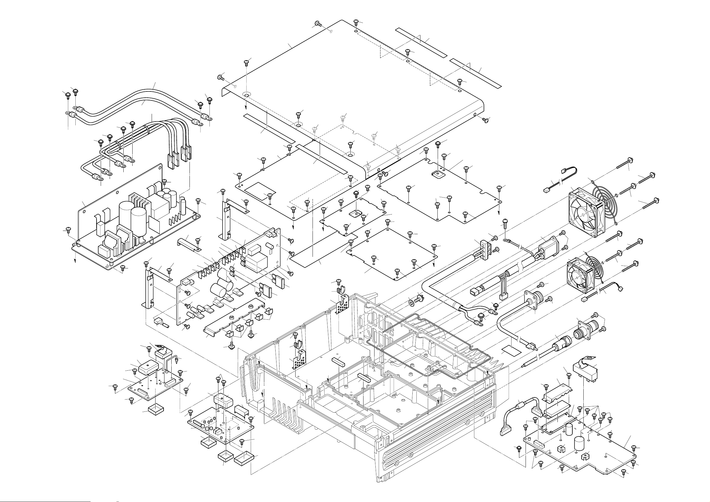
7 - 3
W1
MP100
MP34
W5
MP83
MP35
MP35
MP59
J1
W12
W3
MP33
W10
W11
MP32
EP7 (R)
EP8 (R)
EP4 (R)
EP9 (R)
EP5 (R)
EP3 (R)
EP10 (R)
EP6 (R)
MP33
MP83
MP83
MP83
MP83
MP83
F6 (R)
F2
(R)
F4
(R)
F5
(R)
F1
(R)
MP60
MP60
MP61
MP61
W15
EP4
EP5
MF2
MF1
MP97
W14
MP93
MP94
MP96
MP96
MP28
MP30
MP100
MP100
MP100
MP24
MP21
MP73
MP74
MP103
MP22
MP23
MP36
MP75
F3 (R)
MP64
MP64
MP76
MP104
MP78
MP79
MP75
MP29
MP31
MP70
MP70
MP105
MP50
MP50
MP81
MP90
W13
MP2 (RX)
MP88
MP4
(RX)
MP88
MP88
MP88
MP1 (TX)
MP1 (RX)
MP3 (RX)
MP1
(RVCO)
MP90
MP90
MP90
MP72
MP72
MP54
MP55
MP55
MP54
MP52
MP52
MP72
MP72
MP71
MP90
MP90
MP90
MP2 (TX)
MP1
(PA)
MP63
W6
MP89
MP89
MP80
MP80
MP80
EP1
to EP7 (R)
to EP2 (PA)
to EP1 (PA)
to EP8 (R)
MP80
MP89
MP89
MP58
MP1 (TVCO)
WS1 (TX)
MP63
MP2
(PA)
EP1
(PA)
EP2
(PA)
MP4 (PA)
MP95
MP51
MP59
MP18
MP64
MP64
MP74
MP74
MP74
MP74
MP74
MP74
MP74
MP74
MP74
MP74
MP74
MP73
MP73
MP73
MP73
MP73
MP73
MP73
MP76
MP76
MP76
MP76
MP76
MP76
MP76
MP75
MP75
MP75
MP75
MP90
MP89
MP89
MP64
MP64
MP64
MP64
MP64
MP64
MP90
NOTE
(R): REG UNIT
(RX): RX UNIT
(TX): TX UNIT
(PA): PA UNIT
(RVCO): RVCO UNIT
(TVCO): TVCO UNIT
Par ts without designation are CHASSIS PARTS.
W4
to EP9 (R)
to EP10 (R)
to EP6 (R)
MP53
MP53
MP53
to EP4 (R)
MP53
REG UNIT
A
B
C
D
E
F
E
F
D
C
A
B
TX UNIT
TVCO UNIT
PA UNIT
RX UNIT
RVCO
UNIT

7 - 4
MP1 8510014700 2368 RVCO case 1
REF ORDER
DESCRIPTION
NO. NO.
QTY.
[RVCO UNIT]
MP1 8510014690 2368 TVCO case 1
REF ORDER
DESCRIPTION
NO. NO.
QTY.
[TVCO UNIT]
EP1 6910014490 Terminal OP-100 M3 1
EP2 6910014490 Terminal OP-100 M3 1
MP1 8930060410 2367 Module holde 1
MP2 8930060420 2367 module plate 1
MP3 8510015550 2367 PA shield case assembly Y677 1
REF ORDER
DESCRIPTION
NO. NO.
QTY.
[PA UNIT]
F1 5220000300 Fuse holder 1A5600 1
F2 5220000300 Fuse holder 1A5600 1
F3 5210000850 Fuse ATC-20 1
F4 5220000300 Fuse holder 1A5600 1
F5 5220000300 Fuse holder 1A5600 1
F6 5210000850 Fuse ATC-20 1
EP3 6910011340 Terminal OT-010 M3 1
EP4 6910011340 Terminal OT-010 M3 1
EP5 6910011340 Terminal OT-010 M3 1
EP6 6910011340 Terminal OT-010 M3 1
EP7 6910011340 Terminal OT-010 M3 1
EP8 6910011340 Terminal OT-010 M3 1
EP9 6910011340 Terminal OT-010 M3 1
EP10 6910011340 Terminal OT-010 M3 1
REF ORDER
DESCRIPTION
NO. NO.
QTY.
[REG UNIT]
MP1 8510015120 2368 A-case 1
MP2 8510015130 2368 B-case 1
MP3 8510015140 2368 E-case 1
MP4 8510015480 2367 shield case 1
REF ORDER
DESCRIPTION
NO. NO.
QTY.
[RX UNIT]
MP1 8510015120 2368 A-case 1
MP2 8510015240 2368 TX shield case assembly 1
WS1 8970024070 FX2368 1.5D coaxial cable (1) / TX 1
REF ORDER
DESCRIPTION
NO. NO.
QTY.
[TX UNIT]
J1 6510022970 Connector N-PA-JJ(NI) 1
W1 8900011510 OPC-1048 (AC input cable) 1
W3 8900011531 OPC-1050A (Back up DC cable) 1
W4 8900011540 OPC-1052 (PS output cable) 1
W5 8900011550 OPC-1053 (REG-LOGIC cable) 1
W6 8900011560 OPC-1054 (PA-TX cable) 1
W10 8900011600 OPC-1058 (REG-PA cable red) 1
W11 8900011610 OPC-1059 (REG-PA cable black) 1
W12 8900012150 OPC-1247 (RX-ANT cable) 1
W13 8900012270 OPC-1255 (2367 TX-ANT cable) 1
W14 8900012310 OPC-1265 (REF-FAN/tube) 1
W15 8900011660 OPC-1178 (PA-FAN cable) [FR3000] 1
EP1 6910014470 Unit board FP2152A (100V version) 1
6910014480 Unit board FP2153A (220V version) 1
EP4 6910008330 G80-18 (Fin gured) 1
EP5 8930030420 Cover FG60B 1
MF1 2710000750 Fan FBA08A12LZ 1
MF2 2710000740 Fan FBA06A12L 1
MP18 8110007490 2368 U-cover 1
MP21 8510015490 2367 PA shield cover 1
MP22 8510013770 2368 REG shield cover 1
MP23 8510013790 2368 TX shield cover 1
MP24 8510013780 2368 RX shield cover 1
MP28 8510013810 2368 KC plate Y599 1
MP29 8510013810 2368 KC plate Y599 1
MP30 8010004340 Edging rubber FX452 1
MP31 8010004340 Edging rubber FX452 1
MP32 8930056650 2368 PCB angle Y600 1
MP33 8930056660 2368 REG PCB angle 2
MP34 8410002510 2368 REG heat sink 1
MP35 8930035230 1546 TR-A clip 5
MP36 8930005460 Isolating sheet G 1
MP50 8810000420 Screw PH M4 × 18 2
MP51 8810009030 Screw FH (pan head) M3 × 8 ZK 2
MP52 8810007230 Set screw H M3 × 82
MP53 8810007230 Set screw H M3 × 84
MP54 8810007230 Set screw H M3 × 82
MP55 8810007230 Set screw H M3 × 82
MP58 8810007230 Set screw H M3 × 81
MP59 8810003380 Set screw C M3 × 10 2
MP60 8810010130 Set screw (C) 3 × 35 4
MP61 8810010130 Set screw (C) 3 × 35 [FR3000] 4
8810003360 Set screw C 3 × 6 [FR3100] 4
MP62 8810009040 Set screw H M2.6 × 10 NI 2
MP63 8810004830 Screw PH M3 × 10 surface BS 2
MP64 8810008450 Bind screw M4 × 8 ZK 10
MP70 8810008660 Screw PH BT M3 × 8 NI-ZU 2
MP71 8810008660 Screw PH BT M3 × 8 NI-ZU 1
MP72 8810008660 Screw PH BT M3 × 8 NI-ZU 4
MP73 8810008660 Screw PH BT M3 × 8 NI-ZU 9
MP74 8810008660 Screw PH BT M3 × 8 NI-ZU 12
MP75 8810008660 Screw PH BT M3 × 8 NI-ZU 6
MP76 8810008660 Screw PH BT M3 × 8 NI-ZU 8
MP78 8810008660 Screw PH BT M3 × 8 NI-ZU 1
MP79 8810008660 Screw PH BT M3 × 8 NI-ZU 1
MP80 8810008660 Screw PH BT M3 × 8 NI-ZU 4
MP81 8810008660 Screw PH BT M3 × 8 NI-ZU 2
MP83 8810008660 Screw PH BT M3 × 8 NI-ZU 7
MP88 8810008660 Screw PH BT M3 × 8 NI-ZU 5
MP89 8810008660 Screw PH BT M3 × 8 NI-ZU 6
MP90 8810008660 Screw PH BT M3 × 8 NI-ZU 15
MP93 8820000530 Flange volt M4 × 8 NI 1
MP94 8850000140 Flat washer M4 NI BS 1
MP95 8810003860 Set screw A M4 × 81
MP96 8930059330 Shield sponge (W) 2
MP97 8930059340 2368 A-shield line 1
MP100 8930018620 Himelon sheet Y 4
MP103 8810005770 Set screw Bind M3 × 8 Black 1
MP104 8810005770 Set screw Bind M3 × 8 Black 1
MP105 8930005150 Aluminum sheet B 1
REF ORDER
DESCRIPTION
NO. NO.
[CHASSIS PARTS]
QTY.
Screw abbreviations
B0, BT: Self-tapping PH: Pan head FH: Flat head
NI-ZU: Nickel-Zinc ZK: Black

8 - 1
SECTION 8 SEMI-CONDUCTOR INFORMATION
8 - 1 TRANSISTORS AND FETS
2SC4116-Y
(Symbol: LY)
2SC4215-O
(Symbol: QO)
2SC5006-T1
(Symbol: 24)
2SA1362-Y 2SB1182 TL Q
(Symbol: B1182, Q)(Symbol: AEY)
B
E
C
2SA1576A T106R
(Symbol: FR)
B
E
C
2SC4226-T1 R25
(Symbol: R25)
2SK880Y
(Symbol: XY)
S
D
G
B
E
C
B
E
C
2SC2712-BL
(Symbol: LL)
B
E
C
B
E
C
B
E
C
B
E
C
B
E
C
B
E
C
B
E
C
2SC3661-TB
(Symbol: FY)
2SC4081 T106 R
(Symbol: BR)
2SC4703-T2 SF
(Symbol: SF)
B
CC
E
2SC5337QS-T1
(Symbol: QS)
2SD1664 T100Q
(Symbol: DAQ)
B
CC
E
B
C
E
E
2SJ377 (TE16R)
(Symbol: J377)
G
D
S
G
D
S
B
C
E
B
C
E
2SJ533
(Symbol: J533)
2SJ553STR
(Symbol: J553)
2SK1771 (TE85R)
(Symbol: UB)
D
S
NC
G
2SK3475 (TE12L)
(Symbol: WB)
2SK508 K53 T1B
(Symbol: K53)
D
G
S
DTA143ZUA T106
(Symbol: 113)
B
E
C
B
E
C
DTA144EE TL
(Symbol: 16)
DTC114EUA T106
(Symbol: 24)
B
E
C
B
E
C
B
E
C
DTC144EE TL
(Symbol: 26)
B
E
C
IMZ4 T108
(Symbol: Z4)
E1
B1
C2
C1
B2
E2
XP1111 (TX)
(Symbol: 9S)
XP1114(TX)
(Symbol: 7Q)
E1
B1
B2
C1
C2
E1
B1
B2
C1
C2
XP1214(TX)
(Symbol: 9H)
E1
B1
B2
C1
C2
XP4311 (TX)
(Symbol: 3X)
E1
C2
B1
C1
E2
B2
G
S
D
G
S
D
G
S
D
G
S
D
G
S
D
S
DTC143ZUA T106
(Symbol: 123)
DTC144EUA T106
(Symbol: 26)
2SD1760 TLQ
(Symbol: D1760)

8 - 2
8 - 2 DIODES
1SS226 (TE85R)
(Symbol: C3)
A
C
1SS268 (TE85R)
(Symbol: BF)
C
A1
A2
1SS319 (TE85R)
(Symbol: A4)
A1
A2
C1
C2
A
A
C
C
1SS355 TE-17
(Symbol: A)
AC
AC
AACC
AC
AC
AC
1SV308 (TPL3)
(Symbol: TX)
AC
D1UBA80-4062
(Symbol: UA80)
DSA3A1
(Symbol: None)
FCH30A03L
(Symbol: FCH30A03L)
HSU88TRF
(Symbol: 9)
MA29W-B
(Symbol: Blown line)
brown
MA2S077-(TX)
(Symbol: S)
MA2S111-(TX)
(Symbol: A)
MA8047-M(TX)
(Symbol: 4-7)
AC
AC
NNCD8.2C-T1
(Symbol: None)
PTZ TE25 13B
(Symbol: 13B)
SB07-03C-TB
(Symbol: J)
A
C
A
A
AA
C
C
A
A, C
A, C
A, C
C
Green
1SV305 (TPL3)
(Symbol: TV)
PTZ TE25 36B
(Symbol: 36, B)
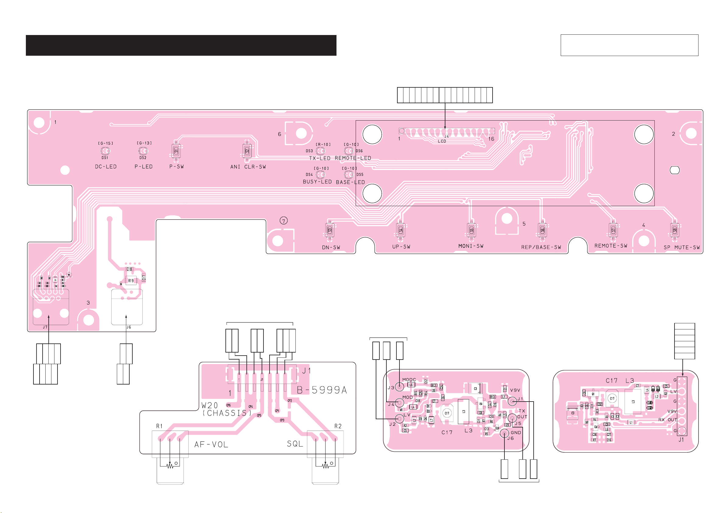
9 - 1
GND
A5V
LCDVRSR/W
ENA
DB0
DB1
DB2
DB3
DB4
DB5
DB6
DB7
BLV
GND
GND
LV
GND
V9V
RX OUT
GND
to LCD DS7
J4
to RX UNIT
VOLUME SQUELCH
MODC
7
MOD
LV
GND
TX OUT
V9V
J3
J1J5J6
J4J2
J1
6
1
to TX UNIT
to TX UNIT
R1 R2
17
28
to SP/MIC
CLONE
M PTT
MIC
M MONI
L9V
SPR
MICE
SPG
13
24
J7 J6
to LINE
L1
NC
NC
L2
12
to LOGIC UNIT
J16
AFVRO
AFG
1123
J15
AFG
AFVRI
J14
SQLVRO
SQLVRI
SQLG
LCD
9 - 2 VR UNIT
¡TOP VIEW
9 - 3 TVCO UNIT
¡TOP VIEW
9 - 4 RVCO UNIT
¡TOP VIEW
9 - 1 FRONT UNIT
SECTION 9 BOARD LAYOUTS
¡ TOP VIEW
The combination of this page and the next page shows
the unit layout in the same configuration as the actual
P. C. Board.

9 - 2
VR UNIT
¡BOTTOM VIEW
TVCO UNIT
¡BOTTOM VIEW
RVCO UNIT
¡BOTTOM VIEW
DCL
TXL
BASEL
D5V
DB7
DB5
ENARSGND
PROG
CHDN
I R/B
to LOGIC UNIT J3
to LOGIC UNIT J4
REMOTE
MICE
GND
CLONE
M MONI
J1 J2
PROGL
RMTL
BUSYL
D5V
DB6
DB4
R/W
A5V
GND
DISP
CHUP
I MONI
1
2
24
23
1
210
9
SPMUTE
MIC
L9V
M PTT
GND
to LOGIC UNIT
J13
1
J8
3
SPG
SPR
1
2
to JACK1
UNIT J3
J9
1
2
1
2
SPR
SPG
1
2
J3
SP1
W18
W19
+
–
L2
TELG
L1
¡¡
BOTTOM VIEW
FRONT UNIT
The combination of this page and the previous page
shows the unit layout in the same configuration as the
actual P.C. Board.

9 - 3
J9
1
345678910111213
11
SPG
SP
to JACK1 UNIT J3
–PTT
+PTT
–AFOUT
+AFOUT
–EXTMOD
+EXTMOD
+BUSY
–BUSY
GND
J11
113
BUSYOUT
TXOUT
COAXSW
M/SO
M/SI
D0
E R/B
E PT2
E MONI
D3/DTO
D4/DTI
D2/RTS
D1/CTS
to JACK2 UNIT J2
J10
113
AF GND
DC GND
AF GND
+E15V
DISC OUT
AF OUT
E MODG
RSSI
E MODG
E MODG
E DTCS
E MOD3
E MOD2
to JACK2 UNIT J3
J13
13
TELGL2L1
to FRONT
UNIT J8
J16
J14
J15
to VR
UNIT J1
1
2
AFVRO
AFG
1
1
7
1
1
1
3
1
2
3
AFG
AFVRI
SQLVRO
SQLVRI
SQLG
SQLVRO
SQLVRI
SQLG
AFVRI
AFG
AFG
AFVRO
9 - 5 LOGIC UNIT
¡¡
TOP VIEW
The combination of this page and the next page shows
the unit layout in the same configuration as the actual
P. C. Board.

9 - 4
DCL
PROGL
TXL
RMTL
BASEL
BUSYL
D5V
D5V
DB7
DB6
DB5
DB4
ENA
R/W
RS
A5V
GND
GND
PROG
DISP
CHDN
CHUP
I R/B
I MONI
J1
1
2
21
22
NDET
SQL
GND
DISC
GND
GND
GND
GND
GND
GND
TUNE
RVCON
RLV
RSSI
W/NS
RUNLK
R9C
RPLSTB
SDTO
SCK
M9V
M9V
J2
1
2
1
1
2
3
4
5
6
7
8
9
10
11
12
13
14
15
30
29
28
27
26
25
24
23
22
21
20
19
18
17
16
2
21
22
to RX UNIT J2
J3
J5
J6
1
14
19
210
2
23
24
to FRONT UNIT J2
to TX UNIT J3
FWSWR
RVSWR
PATEMP
TMUTE2
E TONE
GND
GND
GND
GND
GND
I TONE
TXAF
W/NS
TMUTE1
TLV
TUNLK
TPLSTB
DA1STB
SCK
M9V
M9V
SDTO
9
10
GND
J4
J7
J8
REMOTE
SPMUTE
MICE
MIC
GND
GND
GND
L9V
CLONE
M PTT
M MONI
to FRONT UNIT J1
to OPTIONAL
UNIT
to OPTIONAL UNIT
VCC2
VCC2
to REG UNIT J13
GND
GND2
GND
M9V
L9V
A5V
PSD
M9V
L9V
A5V
REGTEMP
M9C
to REG UNIT J14
MICO
MICI
DISCO
AFOUT
SIGOUT
OPT3
CCS
SDTO
SDTI
SCK
L5V
NC
NC
NC
NC
NC
NC
NC
NC
NC
NC
NC
NC
NC
NC
NC
NC
NC
1
2
3
4
5
6
7
8
9
10
11
12
13
14
15
30
29
28
27
26
25
24
23
22
21
20
19
18
17
16
GND
SIGOUTNCNCNCNCNCNC
NCNCNC
GND
NC
NC
NCNCNC
NCNCNC
NC
NC
L5V
DISCO
OPT1
CCS
CIRQ
SCK
SDTO
SDTI
¡¡
BOTTOM VIEW
LOGIC UNIT
The combination of this page and the previous page
shows the unit layout in the same configuration as the
actual P.C. Board.

9 - 5
to LOGIC UNIT J1
RX ANT
J1
W12
J2
GND
GND
M9V
M9V
R9C
GND
RSSI
GND
RUNLK
RLV
SCK
SDTO
RPLSTB
W/NS
NDET
GND
GND
DISC
GND
TUNE
RVCON
SQL
2
21 1
22
1
2
3
4
5
6
GND
RX OUT
V9V
LV
GND
GND
9 - 6 RX UNIT
¡¡
TOP VIEW
The combination of this page and the next page shows
the unit layout in the same configuration as the actual
P. C. Board.

9 - 6
¡¡
BOTTOM VIEW
RX UNIT
The combination of this page and the previous page
shows the unit layout in the same configuration as the
actual P.C. Board.

9 - 7
to LOGIC UNIT J2
to PA UNIT
J2
21
J3
22
1
2
J5
to PA UNIT J1
10
M9V
M9V
TMUTE2
PCON
PATEMP
RVSWR
FWSWR
GND
GND
GND
1
J4
SCK
SDTO
DA1STB
TPLSTB
M9V
M9V
GND
TUNLK
W/NS
TLV
GND
TMUTE1
GND
FWSWR
RVSWR
PATEMP
TMUTE2
TXAF
GND
ETONE
GND
I TONE
W1
9 - 7 TX UNIT
¡¡
TOP VIEW
The combination of this page and the next page shows
the unit layout in the same configuration as the actual
P. C. Board.

9 - 8
¡¡
BOTTOM VIEW
TX UNIT
The combination of this page and the previous page
shows the unit layout in the same configuration as the
actual P.C. Board.

9 - 9
to TX UNIT J1
W1
TXRFINGND
to TX UNIT J4
10
M9V
M9V
TMUTE2
PCON
PATEMP
RVSWR
FWSWR
GND
GND
GND
1
GND
VCC1
to REG UNIT
EP7
EP2 EP1
to REG UNIT
EP8
TX ANT
W13
IC2
9 - 8 PA UNIT
¡¡
TOP VIEW
The combination of this page and the next page shows
the unit layout in the same configuration as the actual
P. C. Board.

9 - 10
to TX UNIT J1
W1
TXRFIN GND
GND
VCC1
to REG UNIT
EP7
EP2EP1
to REG UNIT
EP8
IC2
¡¡
BOTTOM VIEW
PA U N IT
The combination of this page and the previous page
shows the unit layout in the same configuration as the
actual P.C. Board.

9 - 11
to LOGIC
UNIT J5
to LOGIC UNIT J6
to PA UNIT
EP2
to PA UNIT
EP1
PS 0V PS 15V
BATTERY
–
PS 15V
BATTERY
+
PS 0V
GND
GND
VCC1
VCC1
A5V
REGTEMP
M9C
L9V
M9V
L9V
A5V
PSD
M9V
GND
19
21012
W2 W2
W15
W9 W9
W14
14
J13
M SW
PS 0V
J17
J14
12
GND
PA F12V
J16
to PA FAN
12
GND
PA F12V
J18
to REG FAN
BATTERY
to LOGIC UNIT J11
D-SUB25P JACK
13
13
14 25
1
1
J2
SPG
SPR
SPG
SPR
SPG
–EXTMOD
+EXTMOD
–PTT
+PTT
–AFOUT
+AFOUTSP–BUSY
GND
+BUSY
to LOGIC UNIT J9
to FRONT
UNIT J9
D0
M/SI
M/SO
COAXSW
TXOUT
BUSYOUT
E MONI
E PT2
E R/B
D4/DTI
D3/DTO
D2/RTS
D1/CTS
13
SPG
–EXTMOD
+EXTMOD
–PTT
+PTT
–AFOUT
+AFOUTSP–BUSY
GND
+BUSY
11
2
1
1
1
18
J3
J2
D0
M/S IN
M/S OUT
COAXIAL SW
TX OUT
BUSY OUT
EXT MONI
EXT PTT
EXT RPT/BASE
D4
D3D2D1
RSSI
EXT DTCS
AGND
AGND
AGND
AGND
EXTMOD IN B
EXTMOD IN A
DISC OUT
AF OUT
DC GND
+15V
1
2345678910111213
14 15 16 17 18 19 20 21 22 23 24 25
1234567
8
SPR
–EXTMOD
+EXTMOD
–PTT
+PTT
–AFOUT
+AFOUT
SP
SPG
SP JACK
J1
MODULAR JACK
MODULAR JACK
–BUSY
+BUSY
CHASSIS UNIT
PS 15V
W3 W3
PS 0V
1
1
3
2
1
2
POWER
AC IN
DC SUPPLY
EP1
9 - 11 JACK2 UNIT ¡TOP VIEW
9 - 10 JACK1 UNIT
¡TOP VIEW
9 - 9 REG UNIT
¡¡
TOP VIEW
The combination of this page and the next
page shows the unit layout in the same
configuration as the actual P.C. Board.

9 - 12
JACK1 UNIT
¡BOTTOM VIEW
JACK2 UNIT
¡BOTTOM VIEW
to PA UNIT
EP2
to PA UNIT
EP1
PS 0VPS 15V
BATTERY
–
PS 15V
BATTERY
+
PS 0V
to LOGIC UNIT J10
AF GND
DISC OUT
DC GND
AF OUT
AF GND
E MODG
E MOD2
E MOD3
E MODG
E DTCS
E MODG
RSSI
131
J3
+E15V
¡BOTTOM VIEW
REG UNIT
The combination of this page and the previous page
shows the unit layout in the same configuration as the
actual P.C. Board.

10 - 1
TX
UNIT
SCK,SDTO,DA1STB,TPLSTB
I TONE
TXAF
PATEMP
TLV
TUNLK
FWSWR
RVSWR
IC4D
TXTONE
FIL
Q1: XP1214
CTDTO
from CPU
IC4: NJM2902V
SPLAT
FIL
IC4A, B, C
IC3: NJM2902V
LIMIT
IC3A
SIG
MIX
IC3B
PRE-
EMP
IC2C
CP2
MICO
HPF
IC2A, B
SW-C
IC1C
AF
AMP
IC2: NJM2902V
MIC
MIX
IC2D
IC1D
IC1: NJM2902V
AF
AMP
MICMUTE1
IC13: BU4066BCFV
SW-D
MIC MUTE
MIC
from FRONT UNIT
E MOD1
L9V
M9V
VCC2
REG
UNIT
M9C
PSD
REGTEMP
A5V
IC1B
AF
AMP
E MOD2
from JACK2 UNIT
SW-A
SW-B
IC1A
AF
AMP
CP3
TELAFO
MICMUTE2
TELMUTE1
MICMUTE3
IC14 TC4S66F
RPT
AF
MUTE
AFATTO
R/BSW
from IC41
CP5 CP6 CP9
SIGOUT
CP8
IC26A
IC26: NJM2904V
AF
AMP
IC26B
AF
AMP
RX BPF
TUNE
RPT
AF
ADJ.
A5V
A5V
AFATTI
IC25: M62364FP
RX REF
FREQ
ADJ.
SCK, SDTO, DA2STB
E MOD3
from JACK2 UNIT
E DTCS
from JACK2 UNIT
AFATTO
RUNLK
RLV
M9V
M9V
RVCON
TUNE
TMUTE1, TMUTE2, W/NS
E TONE
RX
UNIT
SCK, SDTO, RPLSTB
SQL
R9C, W/NS
SQL
R2
R1
IC21: TC4W53FU
R/B
SQLO
SW
RSSI
DISC
NDET
BASEL
from IC39
RPT
SQL
ADJ.
DISC
from RX UNIT
IC20:
TC4W53FU
IC16:
TC4W53FU
IC17:
LA4425A
R/B
SQLI
SW
BASEL
from IC39
IC52: NJM2520V
AF
MUTE
AFATTI
to IC25
AFMUTE2
from IC40
IC3C, D
TXSIG
FIL
IC6: NJM2107F
AF
AMP
25TDTMFO, MBEEP, CWO, DTMFO
from CPU
CP4
J7, J8
OPTION
SLOT12
DISCO
MICI
OPT1, OPT3
from IC41
to CPU
from IC40
PROG
ANI CLR
CH UP
CH DN
MONI
RPT/BASE
SP MUTE
REMOTE
DS1
DC
DS2
PROG
LED
CTRL
Q18: XP1114
Q19: XP1114
Q20: XP1114
Q17: DTC144EE
Q24: 2SJ377
from IC39
DISC
from RX UNIT
IC9C: NJM2902V
BUFF
CP1
IC8D
AMP
IC8A–C
IC8: NJM2902V
CTCSS
FIL
IC12D
AMP
IC12A, C
DTCS
FIL
AFOUT
CP10
CP12
CIRQ,CCS,SDTI,SCK,SDTO
IC29: FX805LG
CTCSS
DET
IC9D, B
HPF
IC9A
DEEMP
CP11
CP13
IC7D
AF
AMP
IC10C
AF
AMP
AF OUT
IC7B
AF
AMP
IC10A, B
IC10: NJM2902V
IC9: NJM2902V
LPF
Q37:
DTC144EE
AF
MUTE
TELAFI
VR
UNIT
AFVRI
TELMUTE2
from IC40
KBEEP
from CPU
AF
AMP
AF
MUTE
AFVRO
VOL
AFMUTE1
from IC40
AFOUT1
+ – EXTMOD
IC42, IC43: TLP121 GB
D23–D26: MA2S111
Q44: DTA144EE
E MOD1
SPR
1
2
3
4
5
6
7
8
8P MODULER
CONNECTOR
SP
JACK1
UNIT
EXT SP JACK
+ – AFOUT
+15V
CP26
D1
JACK2
+ – BUSY
I/F
+ – PTT
E PT1
Q7: XP1214
Q8–Q11: XP1111
Q49,Q50: XP4311
D10,D11: MA2S111
D0
D0, D1 ,
D2, D3, D4
BUSYL,TXL
from IC39
BUSYL
RESET
IC34: S-80842CLUA-B363
IC35: BU4011BFV
IC36: BU4011BFV
Q3: DTC144EE
MCK, MDT
IC37: HN58X2464TI
EEPROM
INT, RES
IC33: HD64F2238FA13
AFOUT1
SCK, SDTO, PE1STB
DISCOUT
IC39: BU4094BCFV
PORT
EXPAND
IC7C
AF
AMP
IC7A
IC7: NJM2902V
AF
AMP
DTCSI
to CPU
25TI
to CPU
DTSTD,DTACK,DTMFD
IC31: LC7387M
DTMF
DECODE
X1: CR-733
4.194304 MHz
from CPU
DTSEL2
TELAFO
to IC1A
IC12B
IC12: NJM2902V
25T
FIL
IC30: TC4W53FU
DTMF
SW
DS3
TX
DS5
BASE
DS6
REMOTE
DS7: MSC-C161UYLY-4W
LCD
DS4
BUSY
FRONT UNIT
LOGIC UNIT
1
2
3
4
NC
L1
L2
NC
TEL LINE
CONNECTOR
from CPU
L1
L2
D4: D1UBA80
BRIDGE
D5: D1UBA80
BRIDGE
HOOK
SW
RL1: ATX209
RL2: ATX209
D28: 1SS355
D29: 1SS355
Q38: XP1214
IC46: BA6566F
SPEACH
NET
TELAFI
from CPU
HOOKC
SCK, SDTO, TELSTB
IC47: LC73701M
I/F
DIALER
IC50: TC4W53FU
DTMF
SW
from CPU
DTSEL1
TELBMR
from IC40
SCK, SDTO, PE2STB
SCK, SDTO, PE3STB
BASEL
RMTL
BUSYL
TXL
DCL
PROGL
D5C
TELBUSY
to CPU
IC40: BU4094BCFV
PORT
EXPAND
IC41: BU4094BCFV
PORT
EXPAND
AFMUTE1, 2
MICMUTE1~3
TELMUTE1, 2
TELBMR
R/BSW
W/NS
R9C
OPT1, 3
M9C
CPU
T/RLV
I/F
Q26~Q29: XP4311
D19~D22: MA2S111
E PT1, E PT2
MONI, R/B, M/SI
COAXSW, M/SO
M/SI, E PT2,
E MONI, E R/B
CP20
D4
CP22
D3
CP23
RTS
CP24
D2
13
25
12
24
11
23
10
22
9
21
8
20
7
19
6
18
5
17
4
16
3
15
2
14
1
D-SUB 25PIN
CONNECTOR
UNIT
CP25
CTS
BUSYOUT, TXOUT,
COAXSW, M/SO
CP19
DTI
CP21
DTO
DISCOUT
AF OUT
RSSI
I/F
RXDT0, TXDT0
RTS, CTS
E MOD2
E MOD3
E DTCS
IC32: TC4W53FU
TEMP
SW
D14
MA2S077
SHIFT
SW
X2
CR-681
12.288 MHz
SW
from CPU
SHIFT
from CPU
TEMP
REGTEMP
from REG UNIT
PATEMP
from TX UNIT
IC53: TC4W53FU
T/RLV
SW
TLV
from TX UNIT
RLV
from RX UNIT
IC45: LM567CM
TOUCH
TONE
DECODE
RING
to CPU
ONHOOK
to CPU
RINGER
D1: PTZ36B
IC48: TLP121
IC51: NJNM2107F
AF
AMP
CP28
RXDT1,TXDT1
MIC
CLONE
I/F
Q4, Q6, Q25: 2SC4081
Q5: 2SA1576
D7: MA2S111
M MONI
M PTT
1
2
3
4
5
6
7
8
SP/MIC
CONNECTOR
CLONE
L9V
SPR
from JACK1 UNIT
CHASSIS UNIT
INT SP
SPR
IC11: TA78L05F
+5V
REG
L9V
C5V
IC38: S-812C50AMC
Q45: 2SA1362
D13: SB07-03C
TEL5V L9V C5V
L5V
Q48: IMZ4T108
D43: MA2S111
L9V L5V
: RX LINE
: COMMON LINE
: CONTROL LINE
: DATA BUS
: TX LINE
: CONTROLS LINE
NOTE :
SECTION 10 BLOCK DIAGRAM

10 - 2
T5V
M9V
IC5: M62364FP
T6V +6
REG
+5
REG
M9V
IC1: TA78L05F
IC4: TA78L06F
V9V
Q1: 2SK508
D5: 1SV305
D1: 1SV305
D2: 1SV305
D3: 1SV305
D4: 1SV305
Q6: 2SC3661
D4: MA2S111
TVCO UNIT
Q2: 2SC4226
TX UNIT
D1: 1SV308
D3: 1SV308
Q1: 2SC4215
PATEMP
PA UNIT
M9V+5V
REG
+5V
Q1: 2SK3475
IC7: TA78L05F
IC3: NJM2107F
IC2: S-AV32 (50W type)
S-AV33 (25W type)
D2: HSU88
D4: HSU88
D15: MA29W B
LPF
PWR
AMP
PRE
DRIVE
AMP
AMP
AMP
BUFF
DIV
BUFF
PLL IC
LOOP
FILTER
RIPLE
FILTER
APC
CTRL
PCON
DET
IC1: TA75501F
Q9: DTC143ZU
Q10: DTC114EU
VCC1
SW
TMUTE2
M9V
+9V+9V
Q7: DTC114EU
Q8: 2SA1362
TMUTE1
M9V
M9V
TX OUT
Q3: 2SC5006
SCK/SDTO/TPLSTB
IC2: MB1511PFV
T5V, T6V
MOD
MODC
MOD
MODC
ADJ.
REFMOD
ADJ.
VCOMOD
ADJ.
TLV
Q10: 2SK880
T6V ETONE
ADJ.
TXAF
ADJ.
TONE
ADJ.
MIX
T5V
ETONE
TXAF
TONE
IC6: NJM2107F
M9V
SCK
SDTO
DA1STB
TUNLK
TLV
TMUTE1
TXAF
TONE
ETONE
TMUTE2
PATEMP
RVSWR
FWSWR
TPLSTB
T5V
LOGIC
UNIT
PCON
ADJ.
REF f
ADJ.
PCON
SCK/SDTO/DA1STB
REF
MOD
TUNLK
T5V
IC3: NJM2701F
REFMOD
TVCON
UNLOCK
CTRL
Q7: 2SA1576
Q9: 2SC2712
X1: CR-759
12.8 MHz
TMUTE2
PCON
PATEMP
M9V
RVSWR
FWSWR
VCC1
RVSWR
FWSWR
D7:
FCH30A03L
PS 15V
F3:
ATC20
SW
Q1: 2SJ533
Q4: 2SJ533
M SW
VCC1
REG UNIT
PS 0V
MAIN
VCC1
VCC2
R9V
TUNE
Q1: 2SC5337
IC5: TA75S01F
D3: 1SV305
RX
ANT
TX
ANT
D4: 1SV305
BPF BPF
XTAL
BPF
+5
REG
IF
AMP
CERAMIC
BPF
CERAMIC
BPF
BUFF
RF
AMP
CP17
R5V
IC1: GN2011
FI1: FL-361
31.65 MHz
Q3: 2SK1771
R9V
1st IF
31.65 MHz
IC6: TA78L05F
M9V
2nd MIXER, 2nd IF AMP, FM DET, Noise AMP, SQL CTRL, RSSI
X2:
CR-757
31.195 MHz
2nd LO
D16:
1SS268
FI6:
CFWS455E
455 kHz
2nd IF
455 kHz
IC2: TA31116FN (D)
D15:
1SS268
X1:
CDBC455CX24
HPF
SQL
IC8A: NJM2902V
+5V
+5V
NDET
RSSI
DISC
+5V
+5V
W/N
SW
W/N
SW
Q19:
DTA143ZU
Q1: 2SK508
D2: 1SV305
D3: 1SV305
D4: 1SV305
D1: 1SV305
IC8C: NJM2902V
IC8D: NJM2902V
W/NS
RVCO UNIT
W/N
SW
FI5:
CFWS455G
455 kHz
Q2: 2SC4226
LPF
BUFF
Q8: 2SC4226
Q9: 2SC4703
LPF AMP AMP
AMP
PLL
IC
LOOP
FILTER
BUFF
BUFF
BUFF
DIVATT
R9V
ATT
M9V +6
REG
+5
REG
+6V
IC7: TA78L06F
IC3: TA78L05F
M9V
SW
IC1:
NJM7809FA
Q8: 2SJ553 (S)
Q9: DTC144EE
M9V
L9V
IC3: TA78M05F
A5V
M9C
IC6: TA78L08F
PSD
+8
REG
+9
REG
+9
REG
+5
REG
AMP
IC2: NJM7809DL1A
BACKUP
CTRL
IC7: TA75S393F
IC11: TA75S01F
Q5: 2SD1664
RL2:
D8: MA8047M
Q7: DTC144EE
PS 0V
ACB32101
D4:
FCH30A03L
D3:
DSA3A1
BATT. CHARGE
BATT+
F6:
ATC20
D6: MA29W B
REG
+12
IC9: NJM2107F
A5V
REGTEMP
TA78DL12AF
IC4:
F12V
R9C
R9V
SW
R9V
+5V
Q16: 2SC4081
Q15: 2SB1182 F5
IC4: MB1511PFV
M9V
RXOUT
Q14: 2SC4226
+5V
V9V
RLV
Q18: 2SK880
M9V
RPLSTB
SCK
SDTO
R9C
RUNLK
W/NS
RSSI
RLV
RVCON
TUNE
DISC
SQL
NDET
RUNLK
SCK/SDTO/RPLSTB
+5V, +6V
UNLOCK
CTRL
Q6: 2SC2712
Q7: 2SC2712
+5V
RVCON
X3:
CR-732
12.8 MHz
RX UNIT
A5V
PA F12V
PA F12V
PS 0V
MSW
VCC2
M9C
PSD
REGTEMP
A5V
L9V
M9V
PA
FAN
REG
FAN
CHASSIS UNIT
LOGIC UNIT
W/N
SW
Q22:
2SC4116
Q23:
DTC144EUA
ATT
: RX LINE
: COMMON LINE
: CONTROL LINE
: DATA BUS
: TX LINE
NOTE :

11 - 1
DISPLAY
RX UNIT
CHASSIS UNIT
RVCO
UNIT
TX UNIT
UNIT
TVCO
PA UNIT
FRONT UNIT
JACK1 UNIT
VR UNIT
REG UNIT
LOGIC UNIT
JACK2 UNIT
MICE
to SP MIC
to LINE
M PTT
SPR
CLONE
L9V
1
2
3
4
5
6
7
8
J7
L9V
REMOTE
SPMUTE
MICE
MIC
GND
SPR
SPG
1
2
3
4
5
6
7
8
9
10
J4
1
2
J3
1
2
3
4
5
6
7
8
9
10
J1
W4 (LOGIC)
1
2
3
4
5
6
7
8
9
10
11
12
13
14
15
16
17
18
19
20
21
22
J1
GND
GND
1
2
3
4
5
6
7
8
9
10
11
12
13
14
15
16
17
18
19
20
21
22
J2
W10 (LOGIC)
SPR
SPG
<W18 (CHASSIS), W19 (CHASSIS)>
SP
1
2
RX ANT
RX RFIN
GND
W12 (CHASSIS)
GND
SQL
DISC
GND
TUNE
RVCON
RLV
RSSI
W/NS
RUNLK
R9C
GND
RPLSTB
SDTO
SCK
GND
M9V
M9V
GND
RX OUT
V9V
GND
GND
J1
C99
J2 J1
EP2
EP1
LV
DCL
TELG
L1
L2
CLONE
M PTT
M MONI
GND
PROGL
TXL
1
2
3
J13
1
2
3
4
5
6
7
8
9
10
11
12
13
14
15
16
17
18
19
20
21
22
23
24
J3
1
2
3
J8
1
2
3
4
5
6
7
8
9
10
11
12
13
14
15
16
17
18
19
20
21
22
23
24
J2
W17 (CHASSIS)
W5 (LOGIC)
L2
L1
M MONI
SPG
MIC
1
2
3
4
J6
ANI CLR
PROG
NC
NC
CH DN
CH UP
MONI
RPT/BASE
REMOTE
SP MUTE
D5V
D5V
DB7
DB6
DB5
PROG
RMTL
BASEL
BUSYL
DB4
ENA
R/W
RS
A5V
GND
GND
DISP
CHDN
CHUP
1
2
3
4
5
6
7
8
9
10
11
12
13
14
15
16
17
18
19
20
21
22
J2
GND
NDET
TUNLK
TPLSTB
DA1STB
SDTO
SCK
M9V
M9V
GND
V9V
LV
1
2
3
4
5
6
7
8
9
10
11
12
13
14
15
16
17
18
19
20
21
22
J3
W11(LOGIC)
1
2
3
4
5
6
7
8
9
10
J4
1
2
3
4
5
6
7
8
9
10
J1
W6(CHASSIS)
TXRFOUT
GND
W13 (CHASSIS)
TX ANT
PATEMP
PCON
GND
GND
M9V
M9V
RVSWR
TMUTE2
FWSWR
GND
TXRFIN
GND
WS1(TX)
GND
FWSWR
RVSWR
PATEMP
TMUTE2
GND
E TONE
I TONE
TXAF
GND
W/NS
TMUTE1
GND
TLV
MODC
MOD
TX OUT
GND
SPG
SP
–PTT
+PTT
–EXTMOD
+EXTMOD
–AFOUT
+AFOUT
1
2
3
4
5
6
7
8
9
10
11
J9
I R/B
I MONI
W9(CHASSIS)
SPG
SPR
1
2
J9
W9 (CHASSIS)
1
2
3
4
5
6
7
8
9
10
11
12
13
J3
–PTT
+PTT
–AFOUT
+AFOUT
–EXTMOD
1
2
3
4
5
6
7
8
J2
J1
SP JACK
MODULAR JACK
+EXTMOD
–BUSY
+BUSY
VOLUME
SQUELCH
+BUSY
–BUSY
GND
1
2
3
4
5
6
7
J1
AFVRO
AFG
AFG
AFVRI
SQLG
SQLVRO
1
2
J16
1
2
J15
1
2
3
J14
W16(CHASSIS)
1
2
3
4
5
6
7
8
9
10
J6
L9V
GND
M9V
M9V
L9V
A5V
A5V
REGTEMP
PSD
M9C
1
2
3
4
5
6
7
8
9
10
J14
W3(LOGIC)
VCC1
GND
1
2
J17
EP3, EP10
EP7
EP8
W10(CHASSIS)
W11(CHASSIS)
M SW
PS 0V
W2 (CHASSIS)
W4 (CHASSIS)
1
3
2
1
2
POWER
EP1
DC
SUPPLY
AC IN
BATTERY
BATT–
PS 15V
PS 0V
BATT+
W3 (CHASSIS)
EP4, EP9
EP6
EP5
1
2
3
4
J13
VCC2
VCC2
GND2
GND
W5(CHASSIS)
1
2
3
4
J5
D0
1
2
3
4
5
6
7
8
9
10
11
12
13
J2
COAXSW
E R/B
D4/DTI
D3/DTO
D2/RTS
D1/CTS
M/SI
M/SO
TXOUT
BUSYOUT
1
2
3
4
5
6
7
8
9
10
11
12
13
J11
SQLVRI
W7(CHASSIS)
BUSY OUT
TX OUT
COAXIAL SW
M/S OUT
M/S IN
D0
13
25
12
24
11
23
10
22
9
21
8
20
7
19
6
18
5
17
4
16
3
15
2
14
1
J1
D1
D2
D3
EXT RPT/BASE
EXT PTT
EXT MONI
RSSI
EXT DTCS
AGND
EXTMOD IN B
AGND
EXTMOD IN A
AGND
AF OUT
AGND
DISC OUT
DC GND
+15V
D4
DC GND
E MODG
+E15V
AF GND
AF GND
AF OUT
E MOD2
E MODG
E MOD3
E MODG
E DTCS
RSSI
E MONI
E PT2
DISCOUT
1
2
3
4
5
6
7
8
9
10
11
12
13
J3
1
2
3
4
5
6
7
8
9
10
11
12
13
J10
W8(CHASSIS)
1
2
J16
1
2
J18
GND
GND
PA F12V
PA F12V
W15 (CHASSIS)
W14 (CHASSIS)
PA FAN
REG FAN
1
2
1
2
(50 W Type Only)
SECTION 11 WIRING DIAGRAM

12 - 1
NOTE :
Voltage line
RX line
13
25
12
24
11
23
10
22
9
21
8
20
7
19
6
18
5
17
4
16
3
15
2
14
1
J1
L22 BLM21PG221SN1
L20 BLM21PG221SN10
L18 BLM21PG221SN1
D0
M/S IN
M/S OUT
COAXIAL SW
TX OUT
BUSY OUT
L23 BLM21PG221SN1
L21 BLM21PG221SN1
L19 BLM21PG221SN1
L17 BLM21PG221SN1
D0
M/SI
M/SO
COAXSW
TXOUT
BUSYOUT
1
2
3
4
5
6
7
8
9
10
11
12
13
14
15
J2
E MONI
E PT2
E R/B
D4/DTI
D3/DTO
D2/RTS
D1/CTS
L15 BLM21PG221SN1
L13 BLM21PG221SN1
L11 BLM21PG221SN1
L16 BLM21PG221SN1
L14 BLM21PG221SN1
L12 BLM21PG221SN1
EXT MONI
EXT PTT
EXT RPT/BASE
D4
D3
D2
D1
RSSI
EXT DTCS
AGND
AGND
AGND
AGND
EXTMOD IN B
EXTMOD IN A
DISC OUT
AF OUT
C12
220p
C14
220p
D14
NNCD8.2C
D12
NNCD8.2C
C18
220p
C16
220p
D16
NNCD8.2C
C20
220p
D20
NNCD8.2C
D18
NNCD8.2C
C22
220p
D22
NNCD8.2C
RSSI
1
2
3
4
5
6
7
8
9
10
11
12
13
14
15
J3
C23
220p
D23
NNCD8.2C
D21
NNCD8.2C
C21
220p
C19
220p
D19
NNCD8.2C
C17
220p
D17
NNCD8.2C
C15
220p
C13
220p
L6 BLM21PG221SN1
D15
NNCD8.2C
D13
NNCD8.2C
RSSI
C11
220p
D11
NNCD8.2C
DC GND
+15V
D-SUB25P JACK
AF GND
AF OUT
E MOD2
E MOD3
E DTCS
DISC OUT
L4 BLM21PG221SN1
L2 BLM21PG221SN1
L1 BLM21PG221SN1
L3 BLM21PG221SN1
L5 BLM21PG221SN1
AF OUT
E MOD2
E MOD3
E DTCS
AF GND
E MODG
E MODG
E MODG
DC GND
AF GND
+E15V
DISC OUT
D6
NNCD8.2C
C6
220pC547p
C4
47p
D4
NNCD8.2C
D5
NNCD8.2C
C2
47p
C3
47p
D2
NNCD8.2C
D3
NNCD8.2C
C1
47p
C8
220p
D1
NNCD8.2C
CP1CP2
DC GND
+E15V
to LOGIC UNIT J11
to LOGIC UNIT J10
JACK2 UNIT
J1
1
2
3
4
5
6
7
8
9
10
11
12
13
14
15
J3
SPG
SPR
SP JACK
SPG
SPR
CP1
C13
47p
C14
0.001
1
2
3
4
5
6
7
8
J2
SPG
–EXTMOD
+EXTMOD
–PTT
+PTT
–AFOUT
+AFOUT
SP
L1
L1 – L8
BLM21PG221SN1
L2
L3
L4
L5
L6
L7
SPG
–EXTMOD
+EXTMOD
–PTT
+PTT
–AFOUT
+AFOUT
SP
–BUSY
+BUSY
R8
KU15N14
R10
KU15N14
C10
220p
C12
47p
C11
47p
R6
KU15N14
C8
220pC6220p
R4
KU15N14
C4
220p
C2
220p
R2
KU15N14
MODULAR JACK
–BUSY
+BUSY
L8
R1
KU15N14
R3
KU15N14
R5
KU15N14
R7
KU15N14
R9
KU15N14
C9
220p
C7
220pC5220pC3220p
C1
220p
JACK1 UNIT
1
2
1
2
3
4
5
6
7
8
9
10
11
to FRONT UNIT J9
to LOGIC UNIT J9
123
J9
1
2
3
4
5
6
7
8
9
10
J1
1
2
3
4
5
6
7
8
9
10
11
12
13
14
15
16
17
18
19
20
21
22
23
24
J2
C13
0.001
R27
15
R28
15
C14
0.001
1
2
3
4
1
2
J3
SP1
C16
0.001
C19
0.001
CP3
C15
0.001
C20
0.001
CP1
CP2
R17
47
R18
47
C12
0.001
R15
1.5k
DS4
BG3889S
DS5
BG3889S
DS6
BG3889S
R11
150
R12
150
R13
150
DS1
BG3889S
DS2
BG3889S
DS3
BR-3889S
R10
180
R8
150
R9
150
PTXDC BUSY BASE REMOTE
R21
47k
R22
47k
R23
47k
R24
47k
DS7
MSC-C161UYLY-4W
MIC
M MONI
L1
1µH
Q1 2SC4081
R1
470
R26
47k
C5
0.001
C3
0.001
C2
0.001
R2 10
D1
NNCD8.2C
D3
NNCD8.2C
D2
NNCD8.2C
R3 10
CLONE
M PTT
L9V
MICE
C1
0.001
1
2
3
4
5
6
7
8
9
10
11
12
13
14
15
16
J4
ANI CLR
CH DN
CH DN
S2 SKQDPB
S4 SKQDPB
RPT/BASE
S6 SKQDPB
REMOTE
REMOTE
S7 SKQDPB
SP/MIC
C4
0.001
1
2
3
4
5
6
7
8
J7
SP MUTE
SP MUTE
S8 SKQDPB
MONI
I MONI
S5 SKQDPB
CH UP
CH UP
PROG
S1 SKQDPB
S3 SKQDPB
4
M MONI
SPG
MIC
MICE
M PTT
SPR
CLONE
L9V
I MONI
I R/B
CHUP
CHDN
DISP
PROG
GND
GND
A5V
RS
R/W
ENA
DB4
DB5
DB6
DB7
D5V
D5V
BUSYL
BASEL
RMTL
TXL
PROGL
DCL
I R/B
DISP
PROG
GND
BLV
DB7
DB6
DB5
DB4
DB3
DB2
DB1
DB0
ENA
R/W
RS
LCDV
A5V
GND
DB7
DB6
DB5
DB4
D5V
GND
1
2
3
J8
R19
KU10R29N
C17
0.001
C18
0.001
LINE
1
2
3
4
J6
L2
TELG
L1
L2
TELG
L1
L2
[GEN2], [GEN4],
[EUR2], [FRG2]
L2
TELG
L1
L1
to LOGIC UNIT J3
to LOGIC UNIT J13
SPG
SPG
SPR
SPR
to JACK1 UNIT J3
to LOGIC UNIT J4
REMOTE
SPMUTE
MICE
MIC
GND
L9V
CLONE
M PTT
M MONI
GND
LCDV
ENA
R/W
BS
A5V
GND
RMTL
BASEL
BUSYL
TXL
PROGL
DCL
LCD
SPR
SPG
SPR
SPG
L9V
CLONE
M PTT
MICE
MIC
M MONI
L9V
CLONE
M PTT
MICE
MIC
M MONI
FRONT UNIT
F1
SRB-1A
[USA2]
21
W1
Turn ON: 4.8V
Turn OFF: 0.0V
Turn ON: 2.1V
Turn OFF: 0.0V
Turn ON: 4.8V
Turn OFF: 0.0V
Turn ON: 2.1V
Turn OFF: 0.0V
Turn ON: 4.8V
Turn OFF: 0.0V
Turn ON: 1.8V
Turn OFF: 0.0V
Turn ON: 4.8V
Turn OFF: 0.0V
Turn ON: 2.1V
Turn OFF: 0.0V
Turn ON: 4.8V
Turn OFF: 0.0V
Turn ON: 2.1V
Turn OFF: 0.0V
Turn ON: 4.8V
Turn OFF: 0.0V
Turn ON: 2.1V
Turn OFF: 0.0V
5.0V 0.5V
3.8V
5.0V
5.0V
TX: 0.0V
RX: 4.4V
9.1V
FREE: 4.7V
PUSH: 0.0V
FREE: 4.7V
PUSH: 0.0V
FREE: 4.2V
PUSH: 0.0V
FREE: 4.7V
PUSH: 0.0V
Power supply: DC13.6V
Mesurement Frequency: TX 162.500 MHz, RX 162.125 MHz /
Internal resister of a volt meter: 50 kΩ/V
SECTION 12 VOLTAGE DIAGRAM

12 - 2
NOTE :
Voltage line
RX line
C41
0.001
L33
0.39µH
C182
56p
C39
0.001
L9
458DB-1011
C40
0.001
R15
100
R17
100
R187
100
C35
0.001
C34
0.001
R14
100
G1
6
D1
5
D2
4
S2
3
S1
2
G2
1
IC1
GN2011-Q
W2
L8
458DB-1011
W1
C22
18p
C30
15p
C31
0.001
L7
C6342A-R11J-A
C18
0.001
C24
12p
C21
6p
C152
0.01C30.001
C20
100p
C23
22p
C223
15p
L4
22nH
L6
C6342A-R11J-A
C13
0.001
R4
3.3k
R7
56
R183
10
C19
470p
R5
3.3k
R9
47
Q1
2SC5337
R6
22
[EFR3100]
47
[FR3000]
R185
47
[FR3000]
100
[FR3100]
R186
22 [FR3000]
12 [FR3100]
R184
22
[FR3000]
12
[FR3100]
C210
470p
C7
15p
C5
10p
C6
10p
C8
15p
C12
27p
C220
27p
C221
27p
L2
C6342A-R11J-A
L3
C6342A-R11J-A
L5
22nH
C1
0.01
L1
56nH
C4
27p
C2
27p
R1
82k
[FR3000]
180
[FR3100]
R197
27
[FR3100]
D17
1SS226
R181
SA05C401N
J1
R87
4.7k
W18
R88
47
C120
0.001
3
1
4
5
2
IC5
TA75S01F
R85
10K
CP17
J5
R126
100k
C122
0.001
C142
0.001
R112
1k
C121
0.001
R3
100kD41SV305
R2
100k
D3
1SV305
C205
1p
C206
3p
C183
100p
C110
0.001
C207
22p
C212
220p
C115
0.001
C32
0.001
R81
270
R136
18
C114
22p
C113
39p
L23
82nH
L24
68nH
L12
39nH
L13
47nH
L15
47nH
L39
68nH
C184
22p
C112
39p
L10
458DB-1011
R137
270
C33
0.001
W3 W4
R19
10
IC6
TA78L05F
C43
0.001
C42
0.001
L11
0.1µH
C146
10
R182
10
C213
100p
OGI
OGI
C44
0.01
C141
0.001
Q15
2SB1182
R120
2.2k
R121
2.2k
W6
C140
47
R123
10k
R122
10k
M9V
Q16
2SC4081
R149
10
C116
0.001
C117
0.001
W7
C108
0.001
C187
100p
C109
0.001
R77
10
Q9
2SC4703
C126
0.001
C224
15p
L22
68nH
R75
47
R76
470
C216
10p
C217
10p
L53
56nH
C105
0.001
C106
0.001
R74
2.2k
R72
10
R73
3.9k
C124
33p
L27
15nH
L21
0.22nH
R71
470
R66
18
R6518C104
100p
R68
4.7k
R69
2.2k
Q8
2SC4226
L25
15nH
R70
220
R64
18
CP6
CP9
CP7CP8
CP5
C118
0.001
CP10
C134
100p
R67
10
C103
0.001
C102
47
C226
22
GND
RX OUT
V9V
LV
GND
GND
C138
0.001
R116
4.7k
C186
100p
R117
2.2k
C137
0.001
Q14
2SC4226
Q24
2SC3661
C84
100p
L29
15nH
L30
0.22nH
R119
220
R115
100
R118
10
C188
100p
C52
0.001
M9V
C51
0.001
32
4
1
OUT
GND
GND
IN
6
5
IC7
TA78L06F
C50
10
C53
10
L14
1.2µH
C46
22p
C47
5p
C143
0.001
R35
4.7k
R189
2.7k
C48
0.001
L20
1.5µH
L40
5.6µH
C55
22p
W9
W14
R25
8.2k
C56
0.001
R37
100
Q3
2SK1771
R36
4.7k
W12
W13
W15
L41
BLM21PG221SN1
1
2
3
4
5
6
7
8
9
10
11
12
13
14
15
16
17
18
19
20
21
22
J2
L44
L43
L42
L42 – L51
ACB1608M-600
L45
L46
L47
GND
GND
M9V
M9V
R9C
GND
RSSI
GND
RUNLK to LOGIC UNIT J1
RLV
SCK
SDTO
RPLSTB
W/NS
C58
0.001
X1
CDBC455KCAY24
R155
4.7k
C193
0.1
C57
47
W8
C59
0.001
R61
4.7k
R177
10k
R62
2.2k
C60
47
C67
10
C74
0.1
R39
4.7k
R48
47
C131
0.01
C132
15p
C133
0.001
X2
CR-757
31.165 MHz
R40
10k
R42
10k
D16 1SS268
FI5
CFWS455G
IO
I
O
G
G
C82
0.001
D15 1SS268
C76
0.1
R92
10
C85
0.001
R93
47
C86
0.001
R170
4.7k
12
3
VCC
4
X3
CR-732
12.800 MHz
C87
10
CP12
CP11
R138
1,8k
CP14
CP13
R169
4.7k
R148
3.3k
R190
3.3k
OSCIN
1
OSCOUT
2
VP
3
VCC
4
DO
5
GND
6
LD
7
FIN
8
9
10
CLOCK
11
DATA
13
12
LE
14
FC
15
NCNC
NCNC
16
FOUT
BISW
17
P
18
R
19
20
IC4 MB1511PFV-G-BND
C78
0.1
R49
10k
R168
47k
C83
10
C79
10p
R41
10k
C77
0.1
Q7
2SC2712
R44
4.7k
R43
10k
C75
0.1
R50
47k
Q6
2SC2712
FI6
CFWS455F [FRG2]
CFWS455E [Other]
C73
0.1
R55
22k
R60
100k
C69
0.001
R45
10k
C151
39p
R54
680k
C71 180p
C72
180p
C70
0.1
OSCIN
1
OSCOUT
2
MIXOUT
3
VCC
4
IFIN
5
DEC
6
FILOUT
7
FILIN
8
AFOUT
9
QUAD
10
IFOUT
11
RSSI
12
N-DET
13
N-REC
14
GND
15
MIXIN
16
IC2
TA31136FN
C64
0.001
C62
82p
C199
0.001
C200
0.001
C68
1
C175
22
C174
4.7
C201
10
C204
10
C211
100p
C65
0.001
R63
680
R173
100k
R174
150k
R180
560k
R179
820k
R175
10k
R176
10k
C177
0.1
Q19
DEA143ZUA
IC8
NJM2902V
IC3
TA78L05F
R153 1.8k [Other] : 2.7k [FRG2]
CP18
C173
10
L48
L51
L49
L50
NDET
GND
GND
DISC
GND
TUNE
RVCON
SQL
R56
2.2k
R58
3.3k
R178
100
R191
270k
R194
10k
C225
470p
R167
330k [FR3000]
390k [FR3100]
R57
NTCG16 4BH 103KT
R166
47
R53
100k
R52
47k
R11
5.6k
R10
5.6k
R8
5.6k
C81
10p
C80
10p
CP1
CP3
C159
0.001
R134
1M
R135
100
Q18
2SK880
R140
2.7k
C167
2,2
C198
0.022
R171
10k
C165
2.2
R172
47k
C195
0.001
C196
0.1
R156
33k
R157
100k
R158
10k
Q20
2SA1576
C180
0.01
C181
0.1
R159
1k
R160
4.7k
Q21
2SC4081
C194
0.001
C203
0.1
1
2
3
4
5
6
7
14
13
12
11
10
9
8
R196
180
[FR3100]
C214
7P
C208
18p
C215
0.01
C202
0.001
R195
2.2k
D18
MA2S111
C219
4p
C218
12p
C9
10p
C10
12p
C14
15p
C15
10p
C11
10p
RX UNIT
Q22
2SC4116
R193
47k
R192
4.7k
I
G
O
VCON
OUT
GND
RLV
RVCON
SCK
SDTO
RPLSTB
W/NS
RUNLK
TUNE
SQL
W/NS
W/NS
RPLSTB
SDTO
SCK
RVCON
RLV
RUNLK
TUNE
RX ANT
RX RFIN
W19
[FR3000]
CP2
FI1
FL-361
31.65 MHz
Q23
DTC144EUA
CP4
CP20
C1
0.001
L1
1µH
C2
100p
R13
1k
R1
47
R4
10k
L6
0.22nH
C16
0.001
C27
0.01
C32
0.01
C3
10
V9V
RX OUT
GND
1
2
3
4
5
6
1
2
3
4
5
6
J1
LV
GND
GND
D1
1SV305
D3
1SV305
C7
100p
C17
TZC3Z060A110R00
C11
10p
C8
7p
Q1
2SK508
C6
1p
Q2
2SC4226
C9
10p
C30
0.001
R7
270
R6
3.3k
R3
470
L3
67nH
L4
1µH
C5
0.001
D4
1SV305
D2
1SV305
R2
10
L2
1µH
RVCO UNIT
Power supply: DC13.6V
Mesurement Frequency: RX 162.125 MHz
Internal resister of a volt meter: 50 kΩ/V
2.1V
1.6V
2.1V
2.9V
2.1V
5.0V
9.0V
1.6V
0.7V
1.4V
2.5V
8.3V
4.0V
1.9V
7.4V
1.2V
1.8V
2.9V
5.0V
0.0V
W: 0.5V
N: 5.0V
5.0V
9.0V
5.5V
2.7V
3.9V
1.0V
60 2.3
ANT IN
[dBµ]
RSSI (CP18)
[V]
50 2.3
40 2.1
30 1.9
20 1.6
10 1.4
0 1.2
–10 0.9

12 - 3
NOTE :
Voltage line
TX line
MODC
R95
100
TX OUT
V9V
V9V V9V
GND
GND
MOD
R1
18
R2
18
R3
18
C4
0.001
C77
0.001
R5
3.9k
C2
0.001
R4
10k
C10
8p
C15
0.001
C16
0.001
L2
LQW2BHNR10J01L
R6
100
L14
36CS-656LZ-09K=P3
L31
47nH
C9
10p
C17
0.001
L8
2.2µH
C29
0.001
C20
10p
L9
2.2µH
R17
1.2k
R96
1,2k
R97
680
R16
1k
D1
1SV308D31SV308
to PA UNIT
J2
L10
22nH
C19
10p
J1
R19
4.7k
R20
1k
R91
1k
C32
0.001
R18
10k
C28
47
I
C116
0.001
C117
100p
R21
10
R90
10
M9V
M9V
C27
0.001
C22
18p
C24
0.001
C115
10
C114
0.001
T5V
C26
0.001
C98
47
R51
22k
R52
3.3k
C18
0.001
C21
0.001
R54
1k
R53
100
L11
2.2µH
C1
0.001
C33
47
C60
22
D4
MA2S111
R50
2.2k
R31
4.7k
M9V
R37
2.2k
R32
3.9k
R33
560
C35
0.047
C125
0.1
LV
C92
0.001
R70
1M
R69
100
CP1
CP4
R87
2.2k
C123
10
TUNLK
R92 4.7
C107
100p
T5V
T5V
M9V
MODC
MOD
T6V
C120
0.001
C119
1
R56
47
R9
18
R57
150
R98
10
C57
0.001
R27
10
R34
10k
R26
10
R22
10
C43
0.001
C44
10
C50
10
T6V
C124
0.001
C96
10
C34
0.001
R29
10
C37
0.001
C97
10
L27
BLM21PG221SN1
C85
0.1
C118
100p
1
2
3
4
5
6
7
8
9
10
11
12
J4
GND
GND
FWSWR
RVSWR
PATEMP
PCON
TMUTE2
M9V
M9V
C38
0.001
R23
10
R81
47k
R14
8.2k
R13
10k
OSCIN
2
1
OSCOUT
3
VP
4
VCC
5
DO
6
GND
7
LD
8
FIN
NC
NC
NC
NC
9
CLOCK
12
DATA
13
LE
14
FC
15
BISW
16
FOUT
17
P
18
R
19
20
L17
ACB1608M-600-T
TUNLK
R39
33k
C48
0.001
C49
0.001
C61
0.001
R61
10
LOIN
TUNLK
LOIN
LOIN
5
3412
6
X1
CR-759
12.800 MHz
C58
0.1
R38
100k
C103
0.01
C108
0.001
R41
1k
MIXO
R42
10k
R45
4.7k
R76
4.7k
C36
3.3
R83
47
C52
0.001
R84
6.8k
R85
100k
R78
68k
R77
47k
1
3
2
4
5
R93 220k
C111
0.1
C93
0.001
C100
10
R71
10
R94 100k
C68
0.001
C122
10
C126
56p
C109
10
R86
4.7k
C99
1
SCK
SDTO
DA1STB
TPLSTB
M9V
M9V
1
2
3
4
5
6
7
8
9
10
11
12
13
14
15
16
17
18
19
20
21
22
J3
to LOGIC UNIT
J2
CP3
R88
10k
C110
100p
L28
BLM21PG221SN1
L29
ACB1608M-600
GND
TUNLK
W/NS
TLV
GND
TMUTE1
GND
SCK
DA1
TPL
SDTO
L30 ACB1608M-600
R40 5.6k
R36 5.6k
R35 5.6k
R43 5.6k
FWSWR
RVSWR
PATEMP
TMUTE2
C73
0.001
C74
0.001
C76
0.001
TXAF
GND
E TONE
GND
C69
0.001
L23L22
L22 – L25
ACB1608M-600-T
L24
L26
ACB1608M-600-T
L25
I TONE
VIN1
1
VOUT1
2
VOUT2
3
VIN2
4
VDD
5
LD
6
CLK
7
DI
8
VIN3
9
VOUT3
10
VOUT4
11
VIN4
12
VIN5
13
VOUT5
14
VOUT6
15
VIN6
16
DO
17
VDAREF
18
RESET
19
GND
20
VIN7
21
VOUT7
22
VOUT8
23
VIN8
24
C75 0.001
R79
47k
ETONEO
TXAFO
SCK
SDTO
TXAF
ETONE
PCON
PCON
DA1
SCK
SDTO
DA1
I TONE
I TONEO
W3
W5
R64
47k
TVCON
REFMOD
REFMOD
MODC
TVCON
C80
0.1
C82
10
C51
10
W4
R66
47k
C79
220p
C78
0.001
C104
0.1
C105
10
1
3
2
4
5
R68
10k
R67
220k
R80
10
R24
10
R25
10
L18
ACB1608M-600-T
L19
ACB1608M-600-T
L20
ACB1608M-600-T
L21
ACB1608M-600-T
SCK
SDTO
FWSWR
RVSWR
PATEMP
PCON
TMUTE2
TPL
C47
10p
C46
10p
C45
10p
C39
0.001
C40
0.001
C41
0.001
C42
0.001
TMUTE1
C72
0.001
FWSWR
RVSWR
PATEMP
TMUTE2
10 11
C113
10
C112
100p
C106
0.01
R15
12k
R12
12k
C121
10p
C53
0.1
R10
270
R11
270
C102
22p
G
O
I
G
O
TMUTE1
VCC
VC
GND
GND
OUT
to PA UNIT
J1
W15
W14
CP5
CP6
CP7
CP8
C1
0.001
R13
560
L1
2.2µH
J1
V9V
V9V
R4
10k
L5
2.2nH
C16
0.001
C9
10p
J5
TX OUT
C10
2p
C7
39p
C25
0.001
C17
TZC3R100A110R00
C24
8p
C6
1p
C18
0.001
C12
0.001
J2 J3
LV
L2
1µH
L6
1µH
R12
10k
R14
10k
L4
1µH
W1
D3
1SV305
D5
1SV305
D4
1SV305
D1
1SV305
D2
1SV305
R7
390
R6
3.3kR5220
C13
0.001
J6
J4
MODC
MOD
C8
7p
C11
12p
R15
27k
C3
10
C4
0.001
R2
10
C5
0.001
L7
1µH
L3
35nH
Q2
2SC5006
Q1
2SK508
Q1
2SC4215
Q3
2SC5006
Q5
2SC2712
IC1
TA78L05F
IC4
TA78L06F
Q11
2SA1576A
Q12
2SC4081
Q6
2SC3661
Q10
2SK880
Q9
2SC2712Q72SA1576
IC6
NJM2107F
IC2 MB1511PFV-G-BND
IC3
NJM2107F
TX UNIT
IC5 M62364FP
TVCO UNIT
8.3V
8.3V
2.3V
1.7V
1.0V
5.0V
TX: 3.3V
UNTX: 9.1V
8.9V
6.0V
4.9V
9.1V
2.5V
TX: 4.6V
UNTX:0.0V
1.7V
1.0V
3.4V
2.1V
4.9V
8.3V
Power supply: DC13.6V / Mesurement Frequency TX: 162.500 MHz / Internal resister of the volt meter: 50 kΩ/V

12 - 4
NOTE :
Voltage line
TX line
PA UNIT
R63
1.5k
[FR3000]
1k
[FR3100]
R58
1.5k
D16
HSU88TRF
C112
0.1
[FR3000]
C57
0.1
C11
0.001
C83
1p
C113
4p
D13
HSU88TRF
L15
BLM31PG121SN1
C109
1
[FR3100]
R61
1.5k
[FR3000]
1.2k
[FR3100]
C80
100p
R29
56
C30
0.001
R32
120
R31
120
L8
36CS-656LZ-07K=P3
L19
68nH
L14
1µF
R2222R2322C12
0.001
C32
0.001
to TX UNIT
J1
TXRFIN
J2
C70
0.01
[FR3000]
0.1
[FR3100]
C14
0.001
C16
0.001
C111
0.001
[RF3000]
0.047
[RF3100]
C23
0.001
C38
0.001
C1081C90
0.001
C21
0.001
C56
0.1
C20
0.001
C15
0.001
C78
15p
C79
15p
C44
0.01
C22
0.001
C88 470p
C99
2p
C61
220
T2
CD-CL030H-6R0
VCC1
EP2
to
REG UNIT
EP8
to
REG UNIT
EP7
EP1
GND
TX ANT
TXRFOUT
C55
0.1
C41
0.01
C19
0.001
C74
470p
C53
0.1
C40
0.01
C18
0.001
C67
100
C52
0.1
C37
0.01
C13
0.001
C59
0.1
C47
0.01
C34
0.001
C89
470p
C92
22
C91
0.001
C104
0.01
C95
10p
I
G
O
C96
10
C97
0.01
C101
0.001
C102
0.01
C103
0.1
C105
0.001
C106
0.01
C107
0.1
L20
LA-579
C100
8p
C98
10p
C2
27p
C3
27p
C1
4p
L7
LA-580
L13
LA-536A
L16
BL01RN1A1D2B
Beads
IN
VGG
123
4
VDD
OUT
L10
LA-563A
C48
2p
L6
LA-581
C73
3p
L21
LA-462
C82
0.022
3
5
4
2
1
C110
0.001
C28
0.001
C27
0.001
C25
0.001
C39
0.01
C31
0.001
W3
C26
0.001
D14
HSU88TRF
D7
MA8047
C6910C7110C42
0.01
C24
0.001
C60
10p
C68
4.7
R33
33
R11
5.6k
R28
4.7k
R1
6.8k
R56
47k
R57
1k
R62
270
R47
33k
R16
15k
R15
39k
R19
10
R60
100
2
4
5
3
1
R45
10k
R44
100k
R43
22k
R42
10k
R6
10k
R2 1M
R7
10k
R8
10k
R26
1k
R25
1k
R38 1.2k
R40
100
R20
82
R37
100
R21
82
R41
3.9k
R39
10
R36
100
D4
HSU88TRF
D15
MA29W-B
L18
BLM31PG121SN1
L17
BLM31PG121SN1
D2
HSU88TRF
D6
MA8047
R4
1M
R5
10k
R13
39k
[FR3000]
22k
[FR3100]
GND
RVSWR
FWSWR
to
TX UNIT
J4
PATEMP
PCON
TMUTE2
M9V
M9V
GND
GND
4
5
6
7
8
9
10
3
2
1
11
12
J1
Power supply: DC13.6V
Mesurement Frequency: TX 162.500 MHz
Internal resister of a volt meter: 50 kΩ/V
Power code: 5.5 sq / 50 cm
Hi-Po: 3.6V
Lo-Po: 1.7V
Hi-Po: 0.3V
Lo-Po: 0.0V
Hi-Po: 4.4V
Lo-Po: 3.6V
TX: 3.4V
RX: 0.0V
TX: 9.1V RX: 0.0V
13.6V
TX: 3.4V
RX: 0.0V
9.1V
5.0V
2.9V
Q8
2SA1362-Y
Q7
DTC114EUA
Q10
DTC114EUA
Q9
DTC143ZUA
IC1
TA75S01F
IC2
S-AV32 (I2)
[FR3000]
S-AV33 (I) [FR3100]
IC3
NJM2107F
Q4
2SK3475
IC7
TA78L05F

NOTE :
Voltage line
TX line
RX line
LOGIC UNIT
Q52
2SC2712
Q51
2SD1760
C303
0.1
1
2
3
11
4
R32
22k
R342
3.9k
R340
10
A5V
CP2
R313
100k
R40
4.7k
C7
0.1
C8
0.1
C9
0.1
C11
0.1
C10
0.1
8
9
10
7
6
5
R314
4.7k
R26
15k
R27
5.6k
R28
680
R29
3.9k
R30
2.2k
R31
270
R312
6.8k
R341
3.9k
R5
15k
R6
180k
C382
22p
C287
10
C2
0.0022
R57
1M
R56
1M
R58
1M
R59
1M
14567
8
9
1011121314
IC13
BU4066BCFV
C30
0.1
C32
0.1
R275
100k
R17
4.7k
R469
100
C395
0.1
C397
0.1
R353
4.7k
R64
4.7k
R15
100k
R19
100k
R55
100k
14
13
12
R16
100k
C408
47p
C28
10
C31
1
R18
100k
C33
1
MICMUTE3
MICMUTE1
R277
100k
R306
22k
R7
10k
R278
100k
C27
0.1
8
9
10
14
13
12
IC1D
NJM2902V
IC2D
NJM2902V
IC2C
NJM2902V
IC2B
NJM2902V
IC2A
NJM2902V
IC3A
NJM2902V
IC3C
NJM2902V
IC3D
NJM2902V
IC3B
NJM2902V
IC4A
NJM2902V
IC4C
NJM2902V
IC4D
NJM2902V
IC4B
NJM2902V
IC1C
NJM2902V
IC1B
NJM2902V
IC1A
NJM2902V
IC7A
NJM2902V
IC7B
NJM2902V
IC7C
NJM2902V
IC7D
NJM2902V
R2
100k
C1
1
C364
22p
R3
390k
R355
4.7k
R9
47k
R8
47k
C362
22p
C26
1
C363
0.001
R10
4.7k
W2
C3
10
R494
47k
W14
MIC
E MOD1
R279
100k
C371
0.1
R280
100k
R382
4.7k
C332
0.1
1
2
3
11
4
C23
1
R331
4.7k
1
2
3
11
4
7
6
5
R332
6.8k
R438
10
C283
10
R307
560
R12
47k
R13
47k
C4
4.7
C24
1
C361
0.001
R54
4.7k
R14
4.7k
C25
1
R53
22k
R387
10
CP3
CP4
W15
W16
E MOD2
TELAFO
MICE
R506
560
R52
82k
DISC OUT
A5V
R62
1M
R60
1M
R61
1M
R63
1M
R330
4.7k
R329
100k
C59
1
R435
6.8k
R436
10
1
3
2
4
5
IC6
NJM2107F
C440
0.1
C296
10
R90
100k
TELMUTE1
MICMUTE2
R385
10k
C398
0.1
C34
1
R470
100
C126
10
C58
1
R91
100k
C424
22p
R94
1M
R95
1M
1
2
3
5
4
IC14
TC4S66F
R92
4.7k
SIGOUT
MBEEP
CWO
DTMFO
DTMFO
25TDTMFO
R522
4.7k
C87
0.1
C88
0.1
C129
0.1
C255
0.1
R443
100k
R495
100k
R116
47k
R117
150k
R179
150k
R269
100k
A5V
R349
100
C310
0.1
2
3
11
4
IC10A
NJM2902V
IC10B
NJM2902V
IC10C
NJM2902V
IC10D
NJM2902V
R79
68k
R80
68k
C46
100p
C47
820p
C48
220p
C39
0.1
C40
0.1
C311
0.1
C42
0.1
7
6
5
R325
100k
C43
0.0022
R350
100
R75
220k
1
2
3
11
4
R348
4.7k
R70
2.7k
R71
560
R72
33k
R74
22k
R346
1.2k
R77
4.7k
R347
6.8k
C294
10
R78
68k
C44
39p
C45
560p
CP1
C37
0.1
C36
0.1
C38
0.1
14
13
12
IC9C
NJM2902V
IC9B
NJM2902V
IC9D
NJM2902V
IC9A
NJM2902V
R66
8.2k
R67
5.6k
R68
470
R69
22k
R345
3.3k
R323
100k
R89
4.7k
8
9
10
R65
100k
R88
100k
C307
22p
C451
10
W18
W19
C343
0.01
RL1
ATX209
D28
1SS355
L1
T6
12T01 [USA2]
ATS-007 [Other]
T7
12T01 [USA2]
ATS-007 [Other]
T8
3
2
1
5
4
Q38
XP1214
R411
2.2k
C288
10
IC11
TA78L05F
C389
0.01
C290
10
HOOKC
TELAFI
1
2
3
4
5
6
7
8
IC50
TC4W53FU
R451
100k
CE
1
CK
2
NC
3
DATA
4
RES
5
BUSYOUT
6
OSCI
7
OSCO
8
GND
9
VDD
10
BMR
11
NC
12
TEST
13
DTMF
14
MUTE2
15
MUTE
16
MUTE1
17
DP
18
IC47
LC73701M
R466
1k
C390
0.1
Q40 DTC144EE
W7
R488
2.2k
R474
33k
R473
100k
R476
6.8k
R475 330k
C412
0.001
R477
3.3k
C415
0.1
1
3
2
4
5
IC51
NJM2107F
C417
0.1
C413
0.1
C414
1
C416
0.1
R480
10k
C419
0.01
R479 6.8k
[FR3000]
2.2k [FR3100]
R481
68k [FR3000]
82k [FR3100]
R478
4.7k
R412
47k
OUT FIL
1
LOOPFIL
2
IN
3
VS
4
RT
5
CT
6
GND
7
OUT
8
IC45
LMC567CM
C442
1
C443
0.01
R493
2.2k
W13
C420
10
DP
MUTE
DTMF
TELBMR
TELBUSY
SDTO
SCK
TELSTB
DTMFO
DTSEL1
DTSEL1
ONHOOK
IC49
TLP121
R415
560
R487
560
W8
[FR3000]
[FR3100] only
R414
2.2k
D38
PTZ13B
RL2
ATX209
C346
0.01
D29
1SS355
R486
680
C441
0.47
C375
1
T5
PLA10AS1030R7R2
D5
D1UBA80
D4
D1UBA80
1
2
3
4
5
J13
L2
TELG
R131
27k
D1
PTZ36B
R145
1.8k
R143
1.8k
R529
4.7k
C100
10
C103
0.001
R144
6.8k
IC48
TLP121
R51
10k
TELAFO
C418
0.1
RING
C345
0.001
R148
470k
L9V
2
3
DISC
DISC
DISC
25TI
DISC
C76
0.1
R108
180k
7
6
5
C77
820p
R109
220k
R106
100k
R107
1M
R112
1k
C80
0.047
W20
DISC
A5V
R177
47k
C127
0.022
C128
0.01
C56
0.1
C399
0.1
TELAFO
1
2
3
4
5
6
7
8
IC30
TC4W53FU
C83
0.1
R113
100k
R464
100
C388
0.1
INPUT
1
NC
2
PD
3
OSCO
4
OSCI
5
NC
6
VSS
7
LOADB
8
SD
9
ACK
10
STD
11
EST
12
NC
13
VDD
14
IC31
LC7387M
X1
CR-733
4.194304 MHz
DTACK
DTSTD
DTMFD
DTSEL2
R526
100k
C78
150p
KBEEP
VCC2
GND2
DTMFO
A5V
7
6
5
9
10
R36
100k
R37
100k
R471
100k
R472
100k
C17
680p
C409
0.0022
C18
120p
C20
330p
A5V
R317
100k
1
2
3
11
4
7
6
5
C6
1
C366
22p
R33
100k
R34
100k
R35
100k
C12
560p
C15
680p
R338
10
R118
100k
R119
100k
CP5
CP6
R504
100k
C301
10
C13
82p
C16
68p
C14
220p
R115 82k
R175 100k
R315
100k
C5
1
R316
6.8k
C383 22p
R339
10
R24
4.7k
1
2
3
11
4
C289
10
R496
3.3k
C302
10
R22
10k
R276
10k
R23 330k
R25
4.7k
R318
470k
R441
33k
C373
0.018
R442
33k
C372
68p
R114
39k
C85
1
8
9
10
14
13
12
C125
0.1
C425
0.1
NC
1
VIN1
2
SW1
3
VIN2
4
NC
5
V+
6
VOUT
7
GND
8
IC52
NJM2520V
R505
10
R172
100k
C84
0.001
C124
0.1
AFMUTE2
R123
47k
R124
47k
13
12
R320
47k
R521
47k
R121
150k
R122
39k
C90
0.1
C91
820p
C89
0.018
C92
0.0033
C384
0.1
R457
560
C94
10
1
2
3
4
5
IC17
LA4425A
1
5678
IC16
TC4W53FU
CP15 CP16 CP18
CP17
C97
470
R128
100k
R171
100k
R170
100k
C407
0.1
C123
0.1
C456
0.001
VCC2
SP
SPG
R523
10
R129
10
C96
0.1
C95
470
R86
4.7k
R140
10k
C99
0.1
C98
0.1
R137
10k
R138
10k
R85
10k
8
9
10
R327
100k
R328
4.7k
C340
1
C53
1
C295
10
R141
10k
CP14
AFVRO
AFVRI
R130
33k
R305
33k
R139
33k
R87
4.7k
C54
0.1
R84
10k
1
14
13
12
R81
4.7k
7
6
5
R326
6.8k
R82
68k
R83
68k
C49
220p
C50
150p
C51
15p
C52
150p
TX-SIGNAL FIL
TX-TONE FIL
LPF
A5V
AUDI
AUDO
C396
1
Q37
DTC144EE
CP10
CP11
TELMUTE2
R386
4.7k
R356
6.8k
C330
10
DISC
R391
47k
R390
47k
7
6
5
C421
22p
R389
4.7k
R396
4.7k
R97
470k
R98
470k
R96
120k
C60
0.015
C64
0.001
1
2
3
11
4
IC8A
NJM2902V
IC8B
NJM2902V
IC8D
NJM2902V
IC8C
NJM2902V
R2661kC335
4.7
8
9
10
R397
47k
C337
10
C422
22p
C61
0.015
C62
0.0047
C63
0.0039
R392
100k
R398
47k
R407
100k
R403
4.7k
C339
0.1
R408
10k
R409
10k
R352
100
R99
470k
R100
470k
R102
470k
R321
100k
R101
470k
7
6
5
8
9
10
R103
100k
C308
1
R322
6.8k
R399
100k
C342
0.1
14
13
12
R404
47k
C423
22p
CP12
CP13
TELAFI
R405
100k
C67
330p
C68
220p
C70
0.0015
C71
0.033
C72
56p
C4491C313
0.1
C66
0.012
C341
1
1
3
2
4
5
IC28
NJM2107F
NOTONE
22
WAKE
23
VDD
24
XTAL
1
XTAL/CLK
2
ADDR SELECT
3
21
456789
AUD I
10
AUD O
11
VSS
12
RXAMP I
13
RXAMP I+
14
RXAMP O
15
1617181920
IC29
FX805LG
R105
4.7k
D33
MA2S111
D27
MA2S111
R282
330k
C261
1.5
R285
150k
R281
100k
14
13
12
C266
1
C316
1
R334
4.7k
R463
47
C260
1
C292
10
C386
4.7
C74
4.7
R104
390k
R283
10k
R284
150k
C452
1
C265
10
C263
33p
C262
33p
R304
1M
R300
4.7k
C264
0.001
X3
CR-505
4 MHz
DTCSI
TELAFI
R519
150k
A5V
R293
82k
R294
82k
C274
0.033
R295
56k
C275
0.033
C276
0.0012
R297
33k
C277
0.01
8
9
10
C282
1
R351
100
C312
0.1
R336
100k
R335
4.7k
R292
4.7k
1
2
3
11
4
IC12C
NJM2902V
IC12D
NJM2902V
IC12B
NJM2902V
IC12A
NJM2902V
R337
6.8k
C297
10
14
13
12
C447
1
R520
33k
C448
2.2
R289
68k
C270
0.022
R290
47k
C271
0.047
R291
68k
C272
0.0012
C273
0.0015
AF OUT
AF OUT1
L9V
5678
CP7
SQL
C428
0.1
C429
0.1
C431
0.1
A5V
VIN1
1
VOUT1
2
VOUT2
3
VIN2
4
VDD
5
LD
6
CLK
7
DI
8
VIN3
9
VOUT3
10
VOUT4
11
VIN4
12
VIN5
13
VOUT5
14
VOUT6
15
VIN6
16
DO
17
VDAREF
18
RESET
19
GND
20
VIN7
21
VOUT7
22
VOUT8
23
VIN8
24
IC25
M62364FP
C322
0.1
R453 10
R452
4.7
1
5678
IC20
TC4W53FU
IC21
TC4W53FU
C427
220p
R497
4.7k
R498
4.7k
TXAF
C426
10
C380
0.1
R500
100k
R501
47k
R503
100k
C430
0.1
8
C411
100p
R127
5.6k
14
3
2
1
5
4
Q1 XP1214
C93
0.47
A5V
A5V
DA2STB
SCK
SDTO
I TONE
AFATTI
AFATTO
R376
6.8k
R370
2.2k
R358
2.2k
TUNE
RVCON
A5V
A5V
CTDTO
HPF
PRE-EMPMIC MIX
DE-EMP
HPF
TELEPHONE I/F
S MIX
SPLATTER FILTER
LIMIT
C115
0.47
R165
120k
C117
0.1
C113
220P
R524
560
R166
330k
C116
100P
C118
0.1
123456789
18 10111213141516
TOE
TC
TI1
TI2
MF
MU
RI
RC
AT
17
IC46
BA6566F
C112
0.1
C454
0.0033
[FR3100]
C457
0.22
[FR3100]
R531
10
[FR3000]
10k
[FR3100]
R163
1M
C347
0.1
R162
22k [FR3000]
27k
[FR3100]
R154
39
C108
0.1
R158
1.5k
C107
22
C110
10
R164
33k
R153
10k
R151
47
C106
0.033
R168
470
R489
1k
R492
1.8k
C114
10
R169
390k
R149
1.2k
R150
1.2k
R155
10k
R159
1.5k
R160
1.5k
C111
220
C109
10
E
AC2
AC1
AC1
AC2
E
A5V
A5V
I
G
O
VDD
CONT A
CONT D
I/O
O/I
O/I
I/O
I/O
O/I
O/I
I/O
CONT B
CONT C
VEE
234
1
2
3
4
234
1
2
3
4
J15
TELMUTE2
AFMUTE1
1
2
3
4
5
J14
SQLVRI
SQLVRO
1
2
3
4
J16
AFVRO
SQLG
AFG
AFVRI
AFG
AFG
AFG
AFG
SQLG
SQLVRO
SQLVRI
SQLVRO
SQLVRI
SQLG
R367
4.7k
C323
1
CP9
R369
100k
R371
47k
R359
560
5
6
7
IC26B
NJM2904V
IC26A
NJM2904V
R368
47k
C432
22p
C329
10
R373
4.7k
R50
47k
R48
47k
CP8
E TONE
C326
0.1
R375
100k
3
2
1
4
8
R372
10
C325
10
C328 10
E DTCS
E MOD3
C455
100p
AFATTI
AFOUT
DISCO
MICI
MICO
RB/SW
AFATTO
DISC
BASEL
AUDI
AUDO
CIRQ
SCK
SDTO
CCS
SDTI
DTCSI
A5V
TELAFO
TELAFO
TELAFO
L9V
L9V
DISC
TELAFO
TELAFO
C/DSW
C/DSW
CP2
CP1
SQL
R2
10k-B
CP3
SQLI
SQLO
SQLG
1
2
3
4
5
6
7
8
9
J1
AFG
AFVRI
AFVRO
AFG
CP5
VOL
R1
10k-A
CP4
CP6
VR
UNIT
AUDI
AUDO
L9V
VCC2
GND2
SP, SPG
A5V
DISC
A
B
C
D
E
to FRONT
UNIT J8
GNDRLCLVLPDC
AGC
VCC
RO1
RO2
DISC
F
G
H
I
R528
10k
R527
15
R530
100
C453
4.7
W21
12T01 [USA2]
ATS-007 [Other]
2.0V
2.0V
2.5V
2.0V
2.0V
2.0V
1.9V
2.5V
5.0V
2.5V
13.6V
5.0V
2.0V
MUTE: 0.0V
UN MUTE: 5.0V
VOL Min: 13.2V
VOL Max: 12.5V
2.0V
2.0V
4.1V
12.4ms
5.0V
OFFHOOK: ‘‘H’’
ONHOOK: ‘‘L’’
RING ON TERM: ‘‘L’’
RING OFF TERM: ‘‘H’’
ONHOOK SIGNAL ON TERM: ‘‘L’’
ONHOOK SIGNAL OFF TERM: ‘‘H’’
Power supply: DC13.6V / Mesurement Frequency: TX 162.500 MHz, RX 162.125 MHz / Internal resister of the volt meter: 50 kΩ/V
12 - 5

12- 6
Voltage line
TX line
RX line
LOGIC UNIT
to RX UNIT J2
to TX UNIT J3
L4 BLM31PG121SN1
1
2
3
4
5
6
J5
L9V
VCC2
L1 BLM31PG121SN1
L2 BLM31PG121SN1
L3 BLM31PG121SN1
C249
47
C247
47
C248
10
C234
0.001
C235
0.001
C236
0.001
C237
0.001
C238
0.001
1
2
3
4
5
6
7
8
9
10
J6
C438
0.001
C233
0.001
VCC2
M9V
L9V
A5V
REGTEMP
PSD
M9C
GND2
CP27
D8 MA2S111
D9 MA2S111
D10 MA2S111
D15 MA2S111
D16 MA2S111
R247
100k
D17 MA2S111
D18 MA2S111
C211
47p
C209
47p
C212
47p
C210
47p
R223
1k
RS
PROG
DISP
CHDN
CHUP
MONI
I MONI
M MONI
E MONIE MONI
MBEEP
R246
100k
R225
100k
C200
47p
C199
47p
C201
47p
R201
1k
R222
1k
TMUTE1
TMUTE2
CTS
RTS
M PTT
R/B
REMOTE
SPMUTE
I R/B
E R/B
E R/B
M9VM9V
R200
470
D11
D12
D11, D12, D44–D46
MA2S111
D44
D45
D46
C198
47p
STR
1
D
2
CLK
3
Q1
4
Q2
5
Q3
6
Q4
7
VSS
8
QS
9
QS
10
Q8
11
Q7
12
Q6
13
Q5
14
OE
15
VDD
16
IC39
BU4094BCFV
C251
0.1
R511
47k
R216
1k
CLONE
DCL
PROGL
D5C
BASEL
RMTL
DA1STB
IOE
IOE
IOE
R221
470
R261
47k
C184
47p
C176
47p
C177
47p
IC42
TLP121
M9C M9C
TELBMR
TXL
BUSYL
CLONE
TXL
BUSYL
CLONE
STR
1
D
2
CLK
3
Q1
4
Q2
5
Q3
6
Q4
7
VSS
8
QS
9
QS
10
Q8
11
Q7
12
Q6
13
Q5
14
OE
15
VDD
16
IC41
BU4094BCFV
C253
0.001
C185
47p
C174
47p
C252
0.1
C182
47p
C195
47p
C194
47p
C197
47p
C188
47p
C186
47p
C187
47p
C189
47p
R218
1k
R219
1k
M9C
R/BSW R/BSW
W/NS
R9C
W/NS
R9C
OPT3
OPT1
BUSYL
TXL
E PT1
RUNLK
C/DSW
C204
47p
C203
47p
C202
47p
C205
47p
C206
47p
C208
47p
C169 47p
C170 47p
C168 47p
C171
47p
C207
47p
RPLSTB
TPLSTB
TUNLK
R196
470
R202
470
CWO
COAXSW COAXSW
C214
47p
PB4/A12/TIOCA4
26
PB5/A13/TIOCB4
27
PB6/A14/TIOCA5
28
PB7/A15/TIOCB5
29
PA0/A16
30
PA1/A17/TXD2
31
PA2/A18/RXD2
32
PA3/A19/SCK2
33
P10/TIOCA0/A20
34
P11/TIOCB0/A21
35
P12/TIOCC0/TCLK
36
P13/TIOCD0/TCLK
37
P14/TIOCA1/IRQ0
38
P15/TIOCB1/TCLK
39
P16/TIOCA2/IRQ1
40
P17/TIOCB2/TCLK
41
AVSS
42
P97/DA1
43
P96/DA0
44
P47/AN7
45
P46/AN6
46
P45/AN5
47
P44/AN4
48
P43/AN3
49
P42/AN2
50
P30/TXD0
76
P31/RXD0
77
P32/SCK0/SDA1
78
P33/TXD1/SCL1
79
P34/RXD1/SDA0
80
P35/SCK1/SCL0
81
P36
82
P77/TXD3
P76/RXD3
84
P75/TMO3/SCK3
85
P74/TMO2/MRES
86
P73/TMO1/CS7
87
P72/TMO0/CS6
88
P71/TMRI23
89
P70/TMRI01
90
PG0/IRQ6
91
PG1/CS3/IRQ7
92
PG2/CS2
93
PG3/CS1
94
PG4/CS0
95
PE0/D0
96
PE1/D1
97
PE2/D2
98
PE3/D3
99
PE4/D4
100
CPU
IC33
HD64F2238BFA13
C231
47p
C220
47p
C218
47p
C213
47p
C216
47p
C215
47p
C219
47p
R238
1k
C232
47p
R237
1k
R224
1k
DB7
DB6
DB5
DB4
ENA
KBEEP
CWO
C217
47p
C450
0.1
C5V
CVCC
GND
3
2
1
5
4
Q7 XP1214
COAXSW
M/SO
E MONI
E R/B
R230
47k
C226
47p
R229
47k
C225
47p
R228
47k
C224
47p
R227
47k
C223
47p
D1
D0
E PT2
E PT1
M/SI
M/SI
E PT1
E PT2
D0
D1
3
2
1
5
4
Q8
XP1111
Q9
XP1111
Q10
XP1111
Q11
XP1111
3
2
1 5
4
3
2
1 5
4
KBEEP
NDET
SW
PSD
M/SO M/SO
C221
47p
R243
100k
C130
47p
C135
47p
C134
47p
C133
47p
C132
47p
C131
47p
R236
1k
R235 1k
R512 1k
25TI25TI
DTCSI DTCSI
RSSI
RVSWR
FWSWR
TEMP
CTDTO
M/SI
TXDT2
RXDT2
TXDT2
RXDT2
E PT1
E PT2
D0
D1
D2
D3
D4
SW
T/RLV
PSD
NDET
25TDTMFO
TXDT0
RXDT0
TXDT1 TXDT1
RXDT1 RXDT1
CIRQ CIRQ
SCK
SDTI
SDTO
CCS
DTSTD DTSTD
PE1STB PE1STB
PE2STB PE2STB
PE3STB PE3STB
DA2STB
DTSEL2 DTSEL2
DTSEL1 DTSEL1
DA1STB
NC NC
NC NC
INT
RING
DTMFD
DTACK
DTMFD
DTMFD
DTACK
DTACK
ONHOOK ONHOOK
ONHOOK
IOE IOE
IOE
R214
1k
C173
47p
C172
47p
R215
1k
SHIFT
BUSYL
C156
47p
C157
47p
C158
47p
C160
47p
C155
47p
C161
47p
C159
47p
C162
47p
Q44
DTA144EE
R205
100k
C166
47p
C167
47p
C435
47p
C436
47p
R198
1k
R199
1k
R203
1k
R250
100k
R204
100k
DTSTD
DA1STB
DA1STB
DTACK
DTMFD
CCS
CIRQ
PE3STB
PE2STB
PE1STB
SDTI
DA2STB
IOE
ONHOOK
R197
470
AF GND
VCC2
DC GND
AF GND
D25
D26
R450
390
R460
390
F1 FGB1A
D24
C254
10
R265
1.2k
D23
R262
470
R263
560
IC43
TLP121
T1 12T01
T2 12T01
R264
560
1
2
3
4
5
6
7
8
9
10
11
12
13
J9
1
2
3
4
5
6
7
8
9
10
11
12
13
J10
SPG
SP
–PTT
+PTT
–AFOUT
AFOUT1
+AFOUT
–EXTMOD
+EXTMOD
E MOD1
AF OUT
BUSYOUT
BUSYOUT
+E15V
6
5
4 3
2
1
Q49
XP4311
6
5 2
4 3
1
Q50
XP4311
DISC OUT
DISC OUT
AF OUT
BUSYOUT
TXOUT
E MODG
RSSI
E MODG
E MODG
Q4 2SC4081
R208
47k
Q25
2SC4081
R268
47k
6
5
2
1
Q27 XP4311
D7
MA2S111
CP19
CP20
CP21
R510
10
1
2
3
4
5
6
7
8
9
10
11
12
13
J11
E MOD2
COAXSW
M/SO
M/SI
D0
E R/B
E PT2
E MONI
D3/DTO
D4/DTI
D2/RTS
D1/CTS
D4
D0
COAXSW
M/SO
M/SI
E R/B
E PT2
E MONI
E DTCS
E DTCS
E MOD3
E MOD2
E MOD3
TXOUT
TXOUT
1
3
2
4
5
IC44
NJM2125F
C439
0.1
L9V
TXL
C165
47p
C163
47p
C164
47p
C150
0.1
R206
47k
R213
47k
R212 33k
Q5 2SA1576
Q6
2SC4081
R209 47k
R211
1k
R207
680
C152
47p
C151
47p
C154
47p
C153
47p
D20
MA2S111
R259
100k
D19
MA2S111
6
5
4
3
2
1
Q26 XP4311
D13 SB07-03C
Q45
2SA1362
R417
10
GND
1
VIN
2
VOUT
3
NC
4
NC
5
IC38
S-812C50AMC
C239
470
C433
0.001
L11
BLM31PG121SN1
Q48
IMZ4 T108
R509
10k
R210
33k
DTSEL2
DTSEL1
RXDT0
TXDT0
L5V
L5V
TELBUSY
HOOKC
TELSTB
MDT
MCK
X2
CR-681
12.288 MHz
C139
22p
W1
C143
0.01
R185
12k
R184
1k
C142
0.01
C141
47p
R245
12k
R186
12k
R188
2.7k
R187
2.7k
D6
MA2S111
Q2
2SC4081
R183
100k
R182
100k
C138
47p
R240
1k
D14
MA2S077
R195
47k
Q3
DTC144E
L5
BLM31PG121SN1
R189
1k
A0
1
A1
2
A2
3
VSS
4
SDA
5
SCL
6
WC
7
VCC
8
IC37
HN58X2464TI
TELBUSY
RING
TELSTB
HOOKC
RXDT1
TXDT1
C5V
C140
15p
W17
C242
39p
C145
0.1
C148
0.001
R242
100k
C144
0.1
R193
470k
C137
47p
C136
47p
R190
10k
R191
10k
C147
0.1
C146
0.1
IC35
BU4011BFV
R461
100k
IC36
BU4011BFV
R462
100k
R192
390k
R194
390k
C437
0.1
OUT
1
VDD
2
VSS
3
IC34
S-80842CLUA
C5V
C5V
C5V
TEMP
PATEMP
REGTEMP
T/RLV
SW
PSD
C149
0.1
1
2
3
4 5
6
7
8
IC32 TC4W53FU
R234
47k
C230
47p
R233
47k
C229
47p
R232
47k
C228
47p
R231
47k
C227
47p
R251
100k
1
2
3
6
7
8
IC53 TC4W53FU
RLV
TLV
D3
D2
D4
D2
D3
D4
3
2
1 5
4
L5V
INT
RST
MD2
PSD
RSSI
C240
0.001
C241
10
L5V
RSSI
R260
100k
6
5
4
3
2
1
Q28 XP4311
D23–D26
MA2S111
D22
MA2S111
D21
MA2S111
C434
10
D43
MA2S111
R508
10k
RTS
CTS
6
5
4 3
2
1
Q29 XP4311
CP22
CP23
CP24
CP25
CP26
D3
D2
D1
L9V
83
TXDT0 RXDT0
C/DSW
C/DSW
RUNLK
SCK
SCK
SCK
SCKSCK
SDTO
SDTO
SDTO
SDTOSDTO
SCK
SDTO
16
17
18
19
20
21
22
23
24
25
26
27
28
29
30
1
2
3
4
5
6
7
8
9
10
11
12
13
14
15
16
17
18
19
20
21
22
23
24
25
26
27
28
29
30
1
2
3
4
5
6
7
8
9
10
11
12
13
14
15
C192
47p
C190
47p
C193
47p
C191
47p
R220
1k
PE2STB
SDTO
SCK
AFMUTE1
AFMUTE2
MICMUTE1
MICMUTE2
STR
1
D
2
CLK
3
Q1
4
Q2
5
Q3
6
Q4
7
VSS
8
QS
9
QS
10
Q8
11
Q7
12
Q6
13
Q5
14
OE
15
VDD
16
IC40
BU4094BCFV
C178
47p
C181
0.001
C180
47p
C250
0.1
C179
47p
R217
1k
MICMUTE3
TELMUTE1
TELMUTE2
TELBMR
R257
33k
R256
22
R258
56k
Q24
2SJ377
C244
0.001
Q17
DTC144EE
D5V
D5V
D5C
D5C
3
2
1
5
4
Q18
XP1114
3
2
1
5
4
Q19
XP1114
3
2
1
5
4
Q20
XP1114
DCL
PROGL
TXL
RMTL
BASEL
BUSYL
PROGL
TXL
RMTL
BASEL
BUSYL
L10
BLM31PG121SN1
RVCON
TUNE
SQL
DISC
RSSI
RLV
TXAF
I TONE
E TONE
L9
BLM31PG121SN1
1 2 3 4 5 6 7 8 9 10111213141516171819202122
J1
1 2 3 4 5 6 7 8 9 10111213141516171819202122
J2
Mount B-Side
NDET
SQL
GND
GND
DISC
GND
GND
GND
GND
GND
GND
TUNE
RVCON
RLV
RSSI
W/NS
RUNLK
R9C
RPLSTB
SDTO
SCK
M9V
M9V
NDET
W/NS
RUNLK
R9C
RPLSTB
SDTO
SCK
M9V
FWSWR
RVSWR
PATEMP
TMUTE2
E TONE
GND
GND
GND
GND
I TONE
TXAF
W/NS
TMUTE1
TLV
TUNLK
TPLSTB
DA1STB
SCK
M9V
M9V
TLV
SDTO
TMUTE2
TMUTE1
TUNLK
TPLSTB
DA1STB
SCK
M9V
SDTO
L8 BLM31PG121SN1
R525
1k
CIRQ
SCK
SDTI
SDTO
CCS
L9V
DCGND
VCC2
L5V
L5V
L5V
MICO
MICI
DISCO
AFOUT
SIGOUT
OPT3
OPT1
14
15
3
4
3
CLONE
E PT1
E PT1
RSSI
14
15
TXL
BUSYL
DA1STB
CLONE
C5V
L5V
TXL
BUSYL
CLONE
E PT1
C5V
L5V
L5V
CLONE
E PT1
BUSYL
L5V
P41/AN1
P40/AN0
V REF
AVCC
MD0
MD1
OSC2
OSC1
RES
NM I
STBY
VCC
XTAL
VSS
EXTAL
FWE
MD2
PF7
PF6/AS
PF5/RD
PF4/HWR
PF3/LWR/ADTR
PF2/WA1
PF1/BACK/BUZ
PF0/BREQ/1RQ
51525354555657585960616263646566676869707172737475
DB7
DB6
DB5
DB4
ENARSPROG
DISP
CHDN
CHUP
MONI
MBEEP
C5V
R/B
REMOTE
SPMUTE
MPTT
RTS
CTS
TMUTE2
TMUTE1
TUNLK
TPLSTB
RPLSTB
123456789
101112131415161718192021222324
25
PB3/A11/TIOCD3
PB2/A10/TIOCC3
PB1/A9/TIOCB3
PB0/A8/TIOCA3
PC7/A7
PC6/A6
PC5/A5
PC4/A4
PC3/A3
PC2/A3
PC1/A1
VSS
PC0/A0
CVCC
PD7/D15
PD6/D14
PD5/D13
PD4/D12
PD3/D11
PD2/D10
PD1/D9
PD0/D8
PE7/D7
PE6/D6
PE5/D5
PE3STB
SCK
SCK
SDTO
PE1STB
GND
DCL
L7
BLM31PG121SN1
W12
123456789101112131415161718192021222324
J3
12345678910
J4
CP28
L6
BLM31PG121SN1
L6
DCL
PROGL
TXL
RMTL
BASEL
BUSYL
D5V
D5V
DB7
DB6
DB5
DB4
ENA
R/WRSA5V
GND
GND
PROG
DISP
CHDN
CHUP
I R/B
I MONI
REMOTE
SPMUTE
MICE
MIC
GND
L9V
CLONE
M PTT
M MONI
GND
C/DSW
BASEL
INT
RING
HOOKC
TELSTB
MDT
MCK
TELBUSY
NDET
R241
10
R239
1k
RSSI
RES
1413121110
9
8
1234567
1413121110
9
8
1234567
C5V
GND
GND
MCK
MDT
4 5
123
654
R/BSW
R/BSW R/BSW
A5V
A5V
A5V
25TDTMFO
CTDTO
RVSWR
FWSWR
TEMP
T/RLV
RSSI
E PT1
E PT2
D0
D1
D2
D3
D4
CIRQ
SCK
SDTI
SDTO
CCS
VCC2
to REG UNIT J13
to REG UNIT J14
to OPTIONAL UNIT
to OPTIONAL UNIT
to JACK1 UNIT J3
to JACK2 UNIT J3
to JACK2 UNIT J2
J7
J8
GND
GND2
GND
M9V
L9V
A5V
REGTEMP
PSD
M9C
DCGND
MICO
MICI
DISCO
AFOUT
SIGOUT
OPT3
CCS
SDTO
SDTI
SCK
L5V
L5V
DISCO
SIGOUT
OPT1
CCS
CIRQ
SCK
SDTO
SDTI
SPG
SP
–PTT
+PTT
–AFOUT
+AFOUT
–EXTMOD
+EXTMOD
+BUSY
–BUSY
+E15V
CCS
SDTO
SDTI
SCK
SIGOUT
DISCO
L5V
TELBMR
L9V
VCC2
VCC2
GND2
GND2
M9V
M9V
M9V
VCC2
GND2
VCC2
GND2
VCC2
GND2
A5V
A
B
C
E
D
DISC
L9V
to FRONT UNIT J2 to FRONT UNIT J1
F
G
H
I
NOTE :
Power supply: DC13.6V
Mesurement Frequency: TX 162.500 MHz,
RX 162.125 MHz
Inner resister of the volt meter: 50 kΩ/V
13.6V
3.3V
5.0V
40ms
9.0V
5.0V
4.9V

12 - 7
1
2
3
4
J17
C36
0.001
C4
0.001
R17
22
R3
47k
R66
22k
M SW
C15
0.001
S1
RXE160
R16
22
D7
FCH30A03L
C34
22
R42
10
R27
680
R37
10
C51
0.01
C7
2200
F3
ATC-20
F1 F2
C6
2200
C5
0.001
1
2
3
4
EP3
1
2
3
4
EP10
PS 15V
PS 15V
PS 15V
PS 15V PS 15V
PS 15V
CP5
1
2
3
4
EP4
PS 0V
PS 0V
PS 0V
PS 0V
M SW
PS 0V
W2
W2
W4
W4
PS 0V
R23
12k
R18
10k
R19
10k
R24
3.9k
1
1
2
1
3
4
5
3
2
R41
33k
1
3
4
5
2
R38
10k
C50
0.01
C35
0.01
C33
0.01
RL2
ACB32101
R62
8.2
D2
1SS355
R14
3.3
D4
FCH30A03L
D3
DSA3A1
W4
PS 0V
PS 0V
PS 0V
PS 0V
W2
1
2
3
4
EP7
VCC1
VCC1
VCC2
VCC2
VCC1
1
2
3
4
EP8
1
2
3
4
5
6
J13
C11
0.001
W1
C9
2200
W3
R60
1k
R61
47k
R39
10k
R40
10k
C45
0.01
PS 0V PS 0V
PS 0V
EP9
BATT–
1
2
3
4
EP5
PSD
R59
22k
R58
10k
D8
MA8047 M
C48
0.001
C49
22
PS 0V
PS 0V
1
2
3
4
5
6
7
8
9
10
J14
M9V
M9V
GND
GND
GND
to
LOGIC UNIT
J6
M9V
M9V
L9V
L9V
L9V
D6
MA29W B
REGTEMP
A5V
A5V
A5V
PSD
M9C
M9C
EP2
MMZ1608Y102BT
VCC1
VCC1
VCC1VCC1
PS 0V
BATT+
PS 0V
PS 0V
PS 0V
PS 0V
PS 0V
PS 0V
PS 0V
BATT+
BATT+
F5
BATT+
1
2
3
4
EP6
F6
ATC-20
F4
1
2
3
4
J18
C17
0.001
C19
0.001
L9V
L9VL9V
C37
100
R64
22
R65
4.7k
R31
10
REGTEMP
C42
0.01
R32
10k
C41
22
R68
100
R30
1.2k
R36
100k
1
3
2
4
5
R35
22k
R34
10k
C43
0.01
C52
1
R67
100
R33
3.9k
C25
0.001
A5V
C24
47
C22
0.001
C23
0.001
C47
100
C20
0.001
I
PA F12V
PA F12V
PA F12V
REG FAN
BATTERY
BATTERY
PA FAN
1
2
3
4
J16
C31
0.001
C29
0.001
C28
47
C38
100
C27
0.001
C26
100
I
G
O
G
O
I
G
OI
G
O
I
G
O
to
LOGIC UNIT
J5
to
PA UNIT
EP2
to
PA UNIT
EP1
1
2
POWER
AC IN
1
2
3
4
EP1
Q1
2SJ533
Q4
2SJ533
IC6
TA78L08F
IC7
TA75S393F
IC11
TA75S01F
Q5
2SD1664
Q7
DTC144EE
Q8
2SJ553STR
IC1
NJM7809FA
Q9
DTC144EE
IC9
NJM2107F
IC3
TA78M05F
IC2
NJM7809DL1A
IC4
TA78DL12AF
1
3
21
3
2 1
3
2
1
3
2
CHASSIS UNIT
REG UNIT
DC SUPPLY
AC POWER SUPPLY: 15.4V
DC POWER SUPPLY: 0.0V
AC POWER SUPPLY: 14.8V
DC POWER SUPPLY: 13.6V
12.0V 9.0V
5.0V
5.0V
9.0V
2.8V
8.0V
AC POWER SUPPLY: 0.0V
DC POWER SUPPLY: 5.0V
AC POWER SUPPLY: 15.0V
DC POWER SUPPLY: 13.6V
AC POWER SUPPLY: 15.0V
DC POWER SUPPLY: 13.6V
AC POWER SUPPLY: 15.0V
DC POWER SUPPLY: 13.6V
AC power supply or DC power supply: 13.6V
Mesurement Frequency: RX 162.125 MHz
Internal resister of a volt meter: 50 kΩ/V


1-1-32, Kamiminami, Hirano-ku, Osaka, 547-0003, Japan
S-14004MZ-C1-1
© 2003 Icom Inc.
 Loading...