

Page 1

S-15106XZ-C1
August 2014
VHF TRANSCEIVERS
Page 2
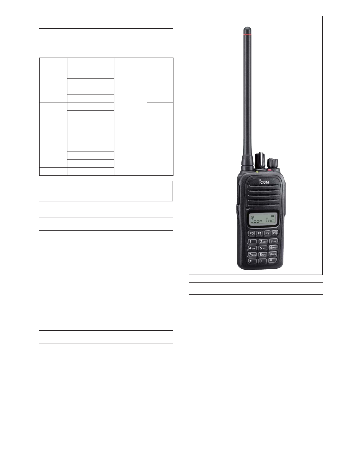
This service manual describes the latest technical information for the IC-F1000 series
VHF TRANSCEIVERS, at the time of
publication.
NEVER connect the transceiver to an AC outlet or to a DC
power supply that uses more than the specifi ed voltage. This
will ruin the transceiver.
DO NOT expose the transceiver to rain, snow or liquids.
DO NOT reverse the polarities of the power supply when con-
necting the transceiver.
DO NOT apply an RF signal of more than 20 dBm (100 mW) to
the antenna connector. This could damage the transceiver’s
front-end.
To upgrade quality, any electrical or mechanical parts
and internal circuits are subject to change without notice
or obligation.
MODEL VERSION
VERSION
NUMBER
FREQUENCY
RANGE (MHz)
KEY TYPE
IC-F1000
USA-01 [#01]
136–174
–
EUR-01 [#02]
UK-01 [#03]
EXP-01 [#04]
IC-F1000S
USA-01 [#05]
4-key
EUR-01 [#06]
UK-01 [#07]
EXP-01 [#08]
IC-F1000T
USA-01 [#09]
10-key
EUR-01 [#10]
UK-01 [#11]
EXP-01 [#12]
IC-F1000T-T THA-01 [#13]
Be sure to include the following four points when ordering
replacement parts:
1. 10-digit Icom part number
2. Component name
3. Equipment model name and unit name
4. Quantity required
<ORDER EXAMPLE>
1110003491 S.IC TA31136FNG IC-F1000 MAIN UNIT 5 pieces
8820001210 Screw 2438 screw IC-F1000S Top cover 10 pieces
Addresses are provided on the inside back cover for your
convenience.
ORDERING PARTS
1. Make sure that the problem is internal before dis-assembling the transceiver.
2. DO NOT open the transceiver until the transceiver is dis-
connected from its power source.
3. DO NOT force any of the variable components. Turn them
slowly and smoothly.
4. DO NOT short any circuits or electronic parts. An insulated
tuning tool MUST be used for all adjustments.
5. DO NOT keep power ON for a long time when the trans-
ceiver is defective.
6. DO NOT transmit power into a Standard Signal Generator
or a Sweep Generator, otherwise the RF power may damage them.
7. ALWAYS connect a 30 dB to 40 dB attenuator between the
transceiver and a Deviation Meter or Spectrum Analyzer,
when using such test equipment.
8. READ the instructions of the test equipment thoroughly
before connecting it to the transceiver.
REPAIR NOTES
INTRODUCTION
CAUTION
(IC-F1000T)
Icom, Icom Inc. and the Icom logo are registered trademarks of Icom Incorporated (Japan) in Japan, the United States, the
United Kingdom, Germany, France, Spain, Russia and/or other countries.
Page 3

TABLE OF CONTENTS
SECTION 1 SPECIFICATIONS
SECTION 2 INSIDE VIEWS
SECTION 3 DISASSEMBLY INSTRUCTION
SECTION 4 CIRCUIT DESCRIPITON
4-1 RECEIVER CIRCUITS ...................................................................................... 4-1
4-2 TRANSMITTER CIRCUITS ............................................................................... 4-2
4-3 FREQUENCY SYNTHESIZER CIRCUITS ....................................................... 4-4
4-4 VOLTAGE BLOCK DIAGRAM ........................................................................... 4-4
4-5 PORT ALLOCATIONS ...................................................................................... 4-5
SECTION 5 ADJUSTMENT PROCEDURES
5-1 PREPARATION ................................................................................................. 5-1
5-2 FREQUENCY ADJUSTMENT .......................................................................... 5-3
5-3 TRANSMIT ADJUSTMENT ............................................................................... 5-4
5-4 RECEIVE ADJUSTMENT ................................................................................. 5-5
SECTION 6 PARTS LIST
SECTION 7 MECHANICAL PARTS
SECTION 8 BOARD LAYOUTS
SECTION 9 BLOCK DIAGRAM
SECTION 10 VOLTAGE DIAGRAM
Page 4

1-1
SECTION 1. SPECIFICATIONS
M GENERAL
• Frequency range: 136–174 MHz
• Number of conventional channels: 16 channels
• Type of emission:
(Occupied band-width)
[EXP], [THA] Wide: 16K0F3E (25.0 kHz)
Narrow: 11K0F3E (12.5 kHz)
[USA] Narrow: 11K0F3E (12.5 kHz)
[EUR], [UK] Wide: 16K0F3E (25.0 kHz)
Middle: 14K0F3E (20.0 kHz)
Narrow: 8K50F3E (12.5 kHz)
• Antenna impedance: 50 (Nominal)
• Operating temperature range: –30˚C to +60˚C: –22˚F to +140˚F (Except [EUR], [UK].)
–25˚C to +55˚C (For [EUR], [UK].)
• Power supply voltage: Specified Icom's battery packs only (7.5 V DC: negative ground)
• Current drain (Approximately): Receiving 77 mA (stand-by)
330 mA (maximum audio, internal speaker)
Transmitting 1.3 A (at 5 W)
• Dimensions:
(Projections not included)
With BP-278
52.2(W)×111.5(H)×22.3(D) mm: 2.1(W) × 4.4(H) × 0.9(D) in
ches
With BP-279
52.2(W)×111.5(H)×24.5(D) mm: 2.1(W) × 4.4(H) × 1(D) inches
• Weight (Approximately): With BP-278
230 g: 8.1
oz.
With BP-279
240 g: 8.5
oz.
• Intermediate frequencies: 1st 46.35 MHz
2nd 450 kHz
• Output impedance (Speaker): 8
• Input impedance (Microphone): 2.2 k
M TRANSMITTER
• Output power: 5 W
• Modulation: Variable reactance frequency modulation
• Maximum frequency deviation: Wide ±5.0 kHz
Middle ±4.0 kHz
Narrow ±2.5 kHz
• Frequency stability: ±2.5 ppm
• Spurious emissions: 70 dB minimum (Except [EUR], [UK].)
0.25 µW (1 GHz), 1.0 µW (1 GHz)
(For
[EUR], [UK].)
• Adjacent channel power: Wide
70 dB minimum, 74 dB typical
Middle
70 dB minimum, 72 dB typical
Narrow
60 dB minimum, 70 dB typical
• Audio harmonic distortion: Wide 1.0% typical at AF 1 kHz 40% deviation
Middle 1.0% typical at AF 1 kHz 40% deviation
Narrow 1.5% typical at AF 1 kHz 40% deviation
• FM hum and Noise:
(Except [EUR], [UK])
(Without CCITT FILTER)
Wide 40 dB minimum, 46 dB typical
Narrow 34 dB minimum, 40 dB typical
• Residual modulation
([EUR], [UK])
:
(With CCITT FILTER)
Wide 45 dB minimum, 50 dB typical
Middle 43 dB minimum, 47 dB typical
Narrow 40 dB minimum, 44 dB typical
• Limitting charact of modulator: 60–100% of maximum deviation
Page 5

1-2
M RECEIVER
• Sensitivity: 0.25 µV typical at 12 dB SINAD (Except [EUR], [UK].)
–4.0 dBµV emf typical at 20 dB SINAD (For [UK], [EUR].)
• Intermodulation: 70 dB minimum, 74 dB typical (Except [EUR], [UK].)
65 dB minimum, 68 dB typical (For [UK], [EUR].)
• Spurious response: 70 dB minimum
• Audio output power: 0.8 W typical at 5% distortion into the 12 internal speaker.
0.4 W typical at 5% distortion into an 8 external speaker.
• Hum and noise (Except [EUR], [UK]):
(Without CCITT Filter)
Wide 40 dB minimum, 51 dB typical
Narrow 34 dB minimum, 45 dB typical
• Hum and noise (For [EUR], [UK]):
(With CCITT Filter)
Wide 45 dB minimum, 52 dB typical
Middle 43 dB minimum, 49 dB typical
Narrow 40 dB minimum, 46 dB typical
• Adjacent channel selectivity: Wide 70 dB minimum, 76 dB typical
Middle 70 dB minimum, 72 dB typical
Narrow 40 dB minimum, 53 dB typical
• Squelch sensitivity: 0.25 µV typical (Except [EUR], [UK].)
–4 dBµV emf typical (For [UK], [EUR].)
Specifications are measured in accordance with TIA-603 or EN 300 086.
All stated specifications are subject to change without notice or obligation.
Page 6
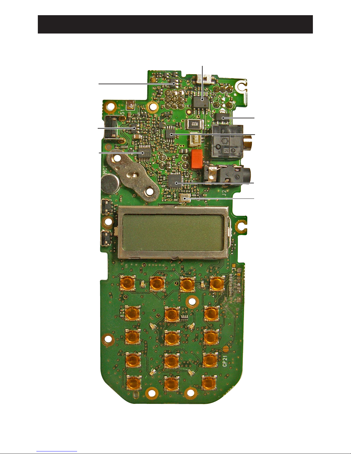
2-1
SECTION 2. INSIDE VIEWS
• MAIN UNIT
(TOP VIEW)
AF POWER AMP
CONTROLLER (Q9)
VOX AMP
(IC3)
BASEBAND IC
(IC4)
BASEBAND IC CLOCK
(X1)
APC AMP
(IC17)
MIC GAIN CONTROLLER
(IC2)
5 V REGULATOR
(IC19)
AF POWER AMP
(IC1)
Page 7
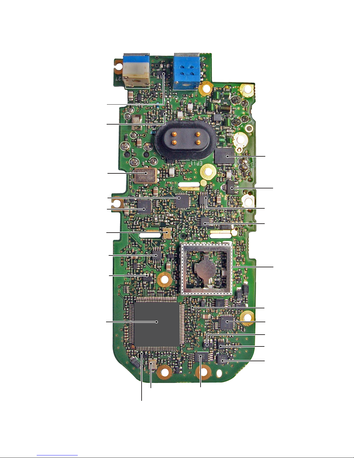
2-2
• MAIN UNIT
(BOTTOM VIEW)
VCO
DRIVE AMP
(Q36)
POWER AMP
(Q38)
AF BUFF/LPF
(IC7)
PLL IC
(IC15)
LED DRIVER
(Q41)
LOGIC CONVERTER
(IC23)
ACCELEROMETER IC
(IC22)
EEPROM
(IC13)
CPU CLOCK
(X2)
RESET IC
(IC8)
CPU
(IC9)
5 V REGULATOR
(IC6)
TONE LPF
(IC5)
REFERENCE
FREQUENCY
OSCILLATOR
(X3)
IF IC
(IC16)
D/A CONVERTER
(IC10)
1ST IF FILTER
(FI1)
3 V REGULATOR
(IC24)
LPF/SUMMING AMP
(IC11)
RF AMP
(Q39)
5 V REGULATOR
(IC20)
Page 8
3-1
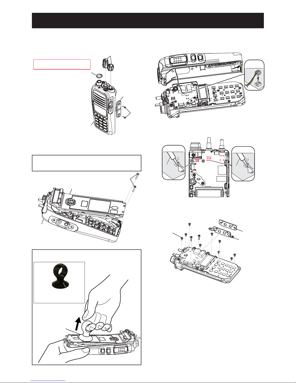
SECTION 3. DISASSEMBLY INSTRUCTION
1. REMOVING THE FRONT PANEL
1) Remove the antenna connector nut and 2 knobs.
2) Remove 2 screws and jack panel.
2. REMOVING THE MAIN UNIT
1) Unsolder total of 15 points as shown.
3) Remove 2 screws from the bottom of the CHASSIS.
4) Lift the bottom of the CHASSIS up in the direction
of the arrow.
2) Remove 11 screws and the side panel and side
seal from the MAIN UNIT.
3) Remove the MAIN UNIT from the chassis.
BE CAREFUL when you disassemble the front panel from
the transceiver body. Otherwise the speaker cable and the
connector may be cut.
Remove with;
“ICOM Driver (K)” (8960000110)
ANTENNA CONNECTOR NUT
JACK PANEL
FRONT PANEL
SCRE
W
KNOB
UNSOLDER
Solder
remover
UNSOLDER
Solder
remover
SCREW×11
SIDE PANEL
SIDE SEAL
FRONT PANEL
CHASSIS
SCREW×2
SPEAKER
CABLE
5) CAREFULLY lift the chassis out of the front panel
and turn it over in order to unplug the speaker cable.
For easy separation of the CHASSIS
Use a suction lifter to lift the bottom of the CHASSIS up.
(Continued to the right above)
Suction lifter
Suction lifter
• Part name : EA950R-2
• Manufacture : ESCO CO.LTD
Page 9
4-1
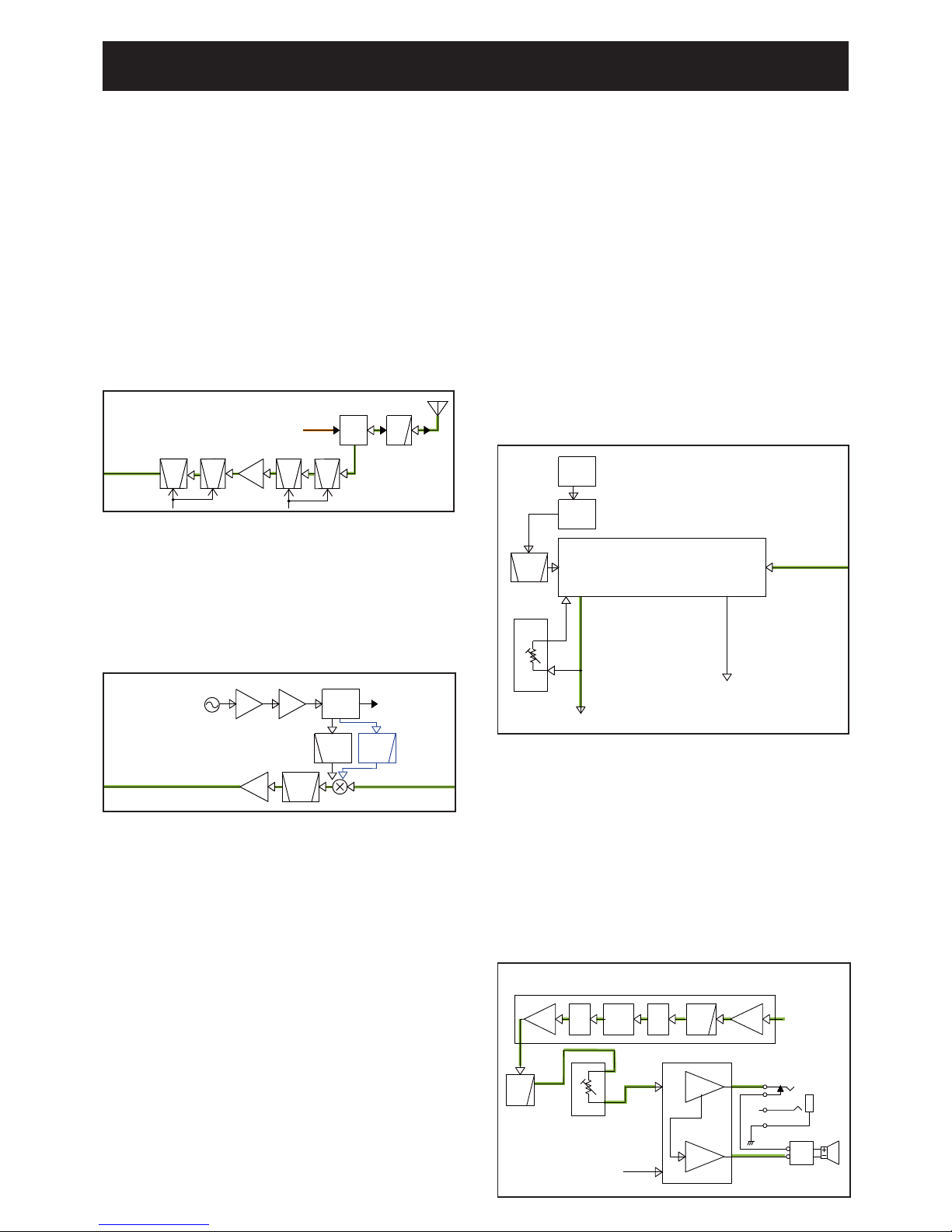
SECTION 4. CIRCUIT DESCRIPTION
• RF CIRCUITS
• 1ST IF CIRCUITS
• 2ND IF CIRCUITS
LPF
ANT
SW
D19,D27
RF
AMP
Q39
BPF
D18
D25
BPF
D31
BPF
D29
BPF
From the TX circuits
1st IF circuits
ANT
T1
T2
TX/RX
SW
D16,D17
Q37
BPF
XTAL
FI1
IF
AMP
Q33
BUFF
Q31
BUFF
Q30
HPF**
LPF*
RX VCO
To the TX circuits
From the RF circuits
To the 2nd IF&demodulator circuits
46.35MHz
1st IF mixer
PLL
IC
IC15
BPF
X3
TCXO
D/A
converter
IF IC
From the 1st IF
circuits
To the RX AF circuits
IC16
15.3MHz
45.9MHz
DISC
SQIN
IC10
NOIS
• RX AF CIRCUITS
Internal speaker
External speaker
From the demodulat
o
circuits
AF
AMP
IC1
J2
SP1
AF
AMP
J3
1
2
LPF
IC11
VOL1
R133
AMPLPFAMP
IC10
AFON
AFO
EMPH
EXP
HPF
IC4
4-1 RECEIVE CIRCUITS
RF CIRCUIT
The RX signal from the antenna is passed through the LPF
(L29 to L31, C333, C347 to C350, C352 and C403) and
antenna SW (D19 and D27) then filtered by the 2-staged
tuned BPF (D25 and D31) to eliminate unwanted out-ofBand signal. The filtered RX signal is amplified by the RF
AMP (Q39), and filtered by another 2-staged tuned BPF
(D18, D29, D36 to D38) to obtain a good image response,
and then applied to the 1st IF circuit.
The tuned BPFs are tuned to the RX frequency by applying adequate tuning voltages (“T1” and “T2”) to the variable
capacitors.
1ST IF CIRCUIT
The RX signal from the RF circuits is applied to the 1st IF
mixer (Q37) and mixed with the 1st LO signal from the RX
VCO, resulting in the 46.35 MHz 1st IF signal. The 1st IF
signal is filtered by the crystal filter (FI1), amplified by the
1st IF AMP (Q33), and then applied to the 2nd IF circuit.
2ND IF CIRCUIT AND DEMODULATOR
The signal from the 1st IF circuits is applied to the IF
demodulator IC (IC16) which contains the 2nd IF mixer, 2nd
IF AMP, FM detector, and so on.
The 1st IF signal is applied to the 2nd IF mixer and mixed
with the 2nd LO signal resulting in the 450 kHz 2nd IF signal.
The 2nd LO signal is generated by tripling the 15.3 MHz
reference frequency signal oscillated by the reference frequency oscillator (X3).
The converted 2nd IF signal is amplified by the 2nd IF AMP,
and then demodulated by the detector circuit.
The demodulated AF signal is applied to the RX AF circuit.
RX AF CIRCUITS
The demodulated AF signal from the IF demodulator IC
(IC16, pin 14) is applied to the baseband IC (IC4).
The processed AF signal is passed through the LPF (IC11),
which attenuates frequencies 3 kHz and above, and adjusted in level by the D/A converter (IC10). The level-adjusted
AF signal is then applied to the AF power AMP (IC1).
The amplified AF signal is applied to the internal or external
speaker.
*:For [EUR] and [UK] versions.
**:F
or except [EUR] and [UK] versions.
Page 10
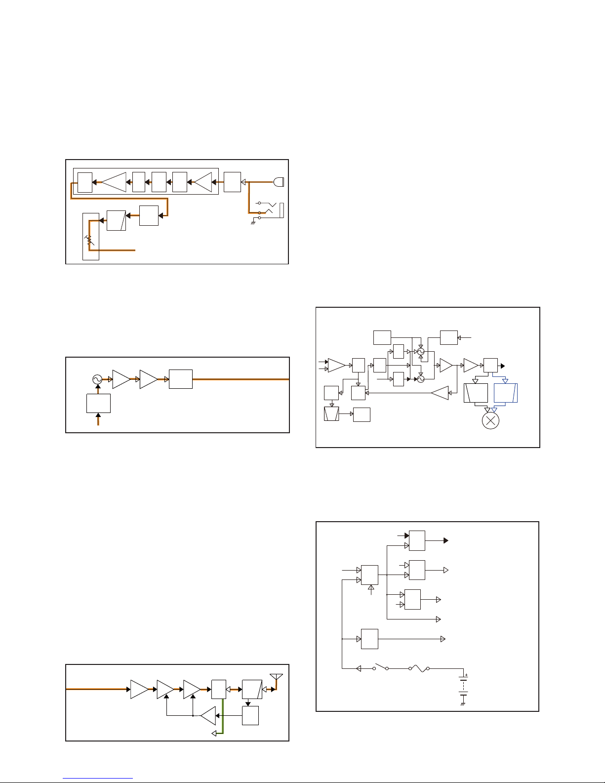
4-3
• TX AF CIRCUIT
• MODULATION CIRCUIT
To the modulation circuit
VOL1
R133
MC1
LPF
IC11
J1
AMP
LIMIT
AMP
MIC
GAIN
IC2
MOD
IC10
AF
SW
EMPH
COMP
SPLT
HPF
IC2
IC4
TX/RX
SW
D16
Q
27,
D
11,D12,D33
FREQUENCY
MODULATION
D13
BUFF
Q31
BUFF
Q30
TX VCO
From the TX AF circuits
To the TX AMP circuits
4-2 TRANSMIT CIRCUITS
TX AF CIRCUIT
The audio signal from the internal or external microphone
(MIC signal) is passed through the MIC gain SW (IC2) and
applied to the baseband IC (IC4).
The processed AF signal is passed through the AF
SW (IC2) and LPF (IC11), and then applied to the D/A
converter (IC10), which adjusts its level (=deviation). The
level-adjusted MIC signal is applied to the TX VCO as the
modulation signal.
MODULATION CIRCUIT
The modulation signal from the TX AF circuits is applied
to D13 of the TX VCO (Q27, D11 to D13 and D33). The
frequency-modulated signal from is amplified by two buffers
(Q30 and Q31), and then applied to the TX AMP circuit,
through the TX/RX SW (D16).
• TX AMPLIFIERS AND APC CIRCUIT
LPF
PWR
DET
D22,D23
ANT
SW
D19,D27
PWR
AMP
Q38
APC
AMP
IC17
DRIVE
AMP
Q36
ANT
From the
TX VCO
To the RX circuits
AMP
PRE
Q34
TX AMP CIRCUIT
The buffer amplified signal from the TX/RX SW (D16)
is sequentially amplified by the pre-AMP (Q34), drive
AMP (Q36) and power AMP (Q38). The power amplified TX
signal is passed through the antenna SW (D19) and LPF
(L29 to L31, C333, C347 to C350, C352 and C403), and
then applied to the antenna.
APC CIRCUITS
At the TX output power detector, the RF signal at the LPF
(L26, C303, C330, C353 and C355) is rectified by the
diodes (D22 and D23), and it is used as the TX power sensing voltage.
The voltage is applied to the APC AMP (IC17), and the
output voltage controls the bias voltages of the drive AMP
(Q36) and power AMP (Q38) to keep the TX output power
constant.
• FREQUENCY SYNTHESIZER CIRCUITS
4-4 VOLTAGE BLOCK DIAGRAM
1st IF mixer
TX/RX
SW
D16
D17
Q25
D9,D10
Q27
D11,D12
FIL
RIPPLE
Q23
VCO
SW
Q29
FIL
LOOP
PLL
IC
IC15
X3
Q26
Q37
BPF
BUFF
Q31
BUFF
Q30
BUFF
Q32
X3
CR-794
TCXO
LV
ADJ
D11
LV
ADJ
D10
BUFF
IC7
IF IC
R5V
RX VCO
TX VCO
IC16
REF
BAL
15.3MHz
45.9MHz
LV
LVA
×2
To the TX AMPs
HPF**
LPF*
To the TX circuits
To the RX circuits
To both RX and TX circuits
To both RX and TX circuits
To the logical circuits
F1
12
T5
REG
Q17
REG
+5V
IC20
REG
S5
Q15
BATTERY_1
BT1
S5
REG
R5
Q16
CPU5
REG
IC6
S5C
VCC
R5C
+5V
T5C
S5V
R5VPWON
VCC
CPU5
T5V
4-3
FREQUENCY SYNTHESIZER CIRCUITS
The RX VCO is composed of Q25, D9, D10 and D32. The
output signal is amplified by two buffers (Q31 and Q31) and
applied to the 1st IF mixer (Q37), through the LO SW (D17)
and LO filter (LPF*: L41, C296 and C441, or HPF**: L21,
L42 and C293).
The TX VCO is composed of Q27, D11 to D13 and D33.
The output signal is amplified by two buffers (Q30 and Q31)
and applied to the pre-AMP (Q34), through the LO SW (D16).
A portion of oscillated VCO output signal from each VCO is
fed back to the PLL IC (IC15), through the buffer (Q32) and
LPF (L11, C210 and C231).
The applied VCO output signal is divided and phasecompared with a 15.3 MHz reference frequency signal from
the TCXO (X3), which is also divided. The resulting signal
is output from the PLL IC (IC15), and DC-converted by the
loop filter, and then applied to the VCO as the lock voltage.
When the oscillation frequency drifts, its phase changes
from that of the reference frequency, causing a lock voltage
change to compensate for the drift in the VCO oscillating
frequency.
*:For [EUR] and [UK] versions.
**:F
or except [EUR] and [UK] versions.
Page 11
4-4
PIN
NO.
LINE
NAME
DESCRIPTION I/O
1 BEEP
Beep audio (Square waves) to the AF
AMP (IC1).
O
2 SENC 2/5 tone and DTMF encoding output. O
17 RMUT
RX AF mute switch control.
L=During the squelch is closed.
O
18 TMUT
Transmission mute.
L=TX inhibit.
O
19 MMUT
MIC mute switch control.
L=MIC mute.
O
20,
21
MGC1*,
MGC0*
MIC gain control. O
22 CL0
Cloning data.
O
23 CLI I
24 CSFT
CPU clock frequency shift control.
H= While the clock frequency is
shifted.
O
25 AUTX
Automatic TX control in the VOX
mode.
H=Microphone input is detected.
O
26 NWC
RX mode (narrow/wide) switching.
L= While receiving in the narrow
mode.
O
27 AFON
AF power AMP control.
H=AF power AMP (IC55) is activated.
O
28 SCK Common serial clock. O
29 S0 Common serial data. O
34 ESCL EEPROM clock. O
35 ESDA EEPROM data. I/O
36 DAST
D/A converter strobe.
H=Load enable.
O
37 PLST
PLL IC strobe.
H=Load enable.
O
38 R5C
Receive circuit power supply line
"R5" control.
H= While the receive circuit is
activated.
O
39 T5C
Transmit circuit power supply line
“T5V” control.
L=While transmitting.
O
40 S5C
TX/RX common circuit power supply
line "S5V" control.
L=While in the power save mode.
O
46 TLED
TX LED indicator control.
L=While transmitting.
O
47 RLED
RX LED Indicator control.
L= While receiving a signal or the
squelch is open.
O
48 LIGT
LCD backlight control.
H=Lights.
O
56,
57
CENC2,
CENC1
CTCSS/DTCS encoding output. O
58 DUSE
AF LPF switching.
H=While sending the DTCS signal.
O
59–
62
CBI0–
CBI3
[R
OTARY SELECTOR] input. O
70 NOIS
Noise level detect.
H=While receiving a signal.
I
71 UNLK
PLL unlock detect.
L=Unlocked.
I
72 KR0
[P0], [1], [2] and [3] input.
L=Pushed.
I
4-5 PORT ALLOCATIONS
• CPU (IC9)
PIN
NO.
LINE
NAME
DESCRIPTION I/O
73 KR1
[P1], [4], [5] and [6] input.
L=Pushed.
I
74 KR2
[P2], [7], [8] and [9] input.
L=Pushed.
I
81 KR3
[P3], [*], [0] and [#] input.
L=Pushed.
I
82 KS0
[P0], [P1], [P2] and [P3] input.
L=Pushed.
I
83 KS1
[1], [4], [7] and [*] input.
L=Pushed.
I
84 KS2
[2], [5], [8] and [0] input.
L=Pushed.
I
85 KS3
[3], [6], [9] and [#] input.
L=Pushed.
I
86 SDEC Decoded 2/5 tone and DTMF signals. I
87 CDEC
Tone signal (CTCSS/DTCS) decoding
input.
I
88 EPTT
External PTT input.
H= An external PTT is pushed.
I
89 IPTT
[PTT] input.
L= Pushed.
I
90 TEMP
Transceiver temperature sensing
voltage.
I
91 BATV Battery voltage. I
92
KRA
[S1], [S2] and [EMER] input.
L= Pushed.
I
93 SDEC2 Decoded 2/5 tone and DTMF signals. I
95 AFVI [VOLUME CONTROL] input. I
96 RSSI
Input port for RSSI signal from the IF
IC (IC16, pin16).
I
97 LVIN Lock voltage input. I
98 MDET
External microphone connection
detect.
I
99 VOXV Microphone input sensing voltage. I
*: MIC sensitivity setting.
Line name MGC0 MGC1 MIC sensitivity
Line state
H H 4 (Maximum)
LH 3
HL 2
L L 1 (Minimum)
Page 12
5-1
SECTION 5. ADJUSTMENT PROCEDURE
M REQUIRED EQUIPMENTS
5-1 PREPARATION
M JIG CABLE
3-conductor 2.5 (d) mm plug
(MIC)
(GND
)
33 k
3-conductor 3.5 (d) mm plug
(CLONE)
OPC-478UC
(GND)
(SP)
[JIG cable1]
[JIG cable2]
+−
AC MILLIVOLTMETER
(10 mV to 10 V)
AUDIO GENERATOR
(300–3000 Hz/1–500 mV)
+−
PTT
+
4.7 µF
EXTERNAL SPEAKER
(1 W/8 Ω)
+
−
SETTING;
Frequency : 1 kHz
Level :150 mV
Waveform : Sine wave
M CONNECTION
FM
deviation meter
to the antenna connector
Attenuator
30 dB
RF power meter
0.1– 10 W/50 Ω
Frequency
counter
Standard signal generator
–20 to 90 dBµ
(–127 to –17 dBm)
NEVER transmit while
an SSG is connected to
the antenna connector.
PC
to USB port
OPC-478UC
Speaker (8 Ω)
To [SP]
To [MIC]
(JIG cable 1)
(JIG cable 2)
IC-F1000/IC-F1000T/
IC-F1000S/IC-F1000T-T
To [SP] connector
EQUIPMENT GRADE AND RANGE EQUIPMENT GRADE AND RANGE
Cloning software
CS-F2000 CLONING SOFTWARE
(Revision 1.0 or later)
JIG cable
Modifi ed OPC-478UC
(See the illust below)
RF power meter
(50 terminated)
Measuring range : 0.1–10 W
Frequency range : 100–300 MHz
SWR : Less than 1.2 : 1
Frequency counter
Frequency range : 0.1–300 MHz
Frequency accuracy : ±1 ppm or better
Input level : Less than 1 mW
Modulation
Analyzer
Frequency range : 30–300 MHz
Measuring range : 0 to ±10 kHz
Standard signal
generator (SSG)
Frequency range : 0.1–300 MHz
Output level : –20 to 90 dBµ
(–127 to –17 dBm)
AC millivoltmeter Measuring range : 10 mV to 10 V
Oscilloscope
Frequency range : DC–20 MHz
Measuring range : 0.01–20 V
Attenuator
Power attenuation : 30 dB
Capacity : More than 10 W
Audio generator
(AG)
Frequency range : 300–3000 Hz
Output level : 1–500 mV
External speaker
Input impedance : 8
Capacity : More than 1 W
Page 13

5-2
M ADJUSTMENT CHANNELS
CONVENIENT: The same cloning file is available.
Right-click below, and select "Save Embeded File to
Disk."
For [EUR] versions:
When adjusting “FM DEVIATION” in the middle band, change the bandwidth to “Middle” as shown below.
Select “Middle”
Page 14

5-3
CTCSS/DTCSS DEVIATION
CTCSS/DTCSS DEVIATION
Click to open the
“I/O Check window”
ADJUST CHANNEL
RX SENSITIVITY
RX SENSITIVITY
ADJUST CHANNEL
MODULATION BALANCE
MODULATION BALANCE
S-METER
REFERENCE FREQUENCY
SQUELCH
LOCK VOLTAGE
LOCK VOLTAGE
TX OUTPUT POWER
TX OUTPUT POWER
FM DEVIATION
FM DEVIATION
If the below window appears, the utility is password-protected.
Enter the password to open the "Adjust Utility" window.
NOTE: The above values for settings are example only.
Each transceiver has its own specifi c values for each setting.
M ADJUSTMENT UTILITY
Page 15

5-4
ADJUSTMENT
TRANSCEIVER’S
CONDITION
OPERATION
ADJUSTMENT
ITEM
VALUE
PLL LOCK
VOLTAGE
-Preparation-
1
–
1) Connect an RF power meter to the
antenna connector.
2) Set the preset adjustment value on the
adjustment utility window.
LV (RX LVA FL) 46
(0.9 V)
LV (TX LVA FL)
LV (RX LVA FH) 255
(5.0 V)
LV (TX LVA FH)
-ADJUSTMENT(RX Band low)
2• Select the item [RX LVA Start], then push [ENTER] to enter the
lock voltage adjustment mode.
[RX LVA Start]
–
3 • Channel: 1-1
• Receiving
• Select the item [RX LVA FL], then push
[ENTER].
[RX LVA FL]
0.9 V
4• Select the item [RX LVA Start], then push [ENTER]. [RX LVA Start] –
(RX Band high) 5 • Channel: 1-2
• Receiving
• Set the item adjustment value in the [RX
LVA FH] on the adjustment utility window,
then push [ENTER].
[RX LVA FH]
255
(5.0 V)
6• Select the item [RX LVA Start], then push [ENTER] to quit the
lock voltage adjustment mode.
[RX LVA Start]
–
-ADJUSTMENT(TX Band low)
7• Select the item [TX LVA Start], then push [ENTER] to enter the
lock voltage adjustment mode.
[TX LVA Start]
–
8 • Channel: 1-1
• Receiving
• Select the item [TX LVA FL], then push
[ENTER].
[TX LVA FL]
0.9 V
9• Select the item [TX LVA Start], then push [ENTER] to quit the
lock voltage adjustment mode.
[TX LVA Start]
–
(TX Band high) 10 • Channel: 1-2
• Receiving
• Set the item adjustment value in the [TX
LVA FH] on the adjustment utility window,
then push [ENTER].
[TX LVA FH]
255
(5.0 V)
11
• Select the item [TX LVA Start], then push [ENTER] to quit the
lock voltage adjustment mode.
[TX LVA Start]
–
PLL LOCK
VOLTAGE
-Verify(RX Band low)
1 • Channel: 1-3
• Receiving
• Click the [Reload (F5)] button to check on
the "I/O Check window" as below.
[LVIN]
(On the "I/O
Check window")
0.9 V ±0.2 V
(Verify)
(RX Band high) 2 • Channel: 1-4
• Receiving
Less than
3.5 V
(Verify)
(TX Band low) 3 • Channel: 1-3
• Transmitting
0.9 V ±0.2 V
(Verify)
(TX Band high) 4 • Channel: 1-4
• Transmitting
Less than
3.5 V
(Verify)
REFERENCE
FREQUENCY
1 • Channel: 1-5
• Transmitting
• Loosely couple a frequency counter to the
antenna connector. [REF]
174.000000
MHz
(±150 Hz)
5-2 FREQUENCY ADJUSTMENTS
1) Select an adjustment item using []/[] on the PC's keyboard.
2) Set or modify the adjustment value as specifi ed using []/[] on the PC's keyboard, and then push [ENTER].
• I/O Check window
(The values shown above are only examples.
Each transceiver has own values.)
* * *
Lock voltage
Page 16

5-5
5-3 TRANSMIT ADJUSTMENTS
1) Select an adjustment item using []/[] on the PC’s keyboard.
2) Set or modify the adjustment value as specifi ed using []/[]on the PC’s keyboard, and then push [ENTER].
ADJUSTMENT
TRANSCEIVER’S
CONDITION
OPERATION
ADJUSTMENT
ITEM
VALUE
TX OUTPUT
POWER
1 1) Connect an RF power meter to the antenna connector.
2) Select [Power Start], then push [ENTER] to enter the TX out-
put power adjustment mode.
[Power Start]
–
(High power,
Band low)
2 • Channel: 1-6
• Transmitting
1) Adjust the TX output power.
2) Select the item [Power Start], then
push [ENTER] to store the adjustment
value.
[Power (FL)] 5.0 W
(High power,
Band center)
3 • Channel: 1-7
• Transmitting
[Power (FC)]
(High power,
Band high)
4 • Channel: 1-8
• Transmitting
[Power (FH)]
5• Select [Power Start], then push [ENTER] to quit the TX output
power adjustment mode.
[Power Start]
–
(L2 power,
Band low)
4 • Channel: 1-9
• Transmitting
• Adjust the TX output power.
[Power (L2)]
2.0 W
(L1 power,
Band low)
5 • Channel: 1-10
• Transmitting
[Power (L1)]
1.0 W
FM DEVIATION
-Narrow(Band low)
1 • Set [MIC gain] to “2” in the Set mode. [Mic Gain] 2
2• Connect a modulation analyzer with an oscilloscope to the an-
tenna connector through an attenuator, and set it as:
HPF: OFF
LPF: 15 kHz or 20 kHz
De-emphasis: OFF
Detector: (P–P)/2
• Connect an audio generator to the [MIC] jack through the JIG
cable, and set it as:
Frequency: 1 kHz
Waveform: Sine wave
Level: 150 mVrms
––
3• Select [MOD Start], then push [ENTER] to enter the TX output
power adjustment mode.
[MOD Start]
–
4 • Channel: 1-11
• Transmitting
1) Adjust the deviation.
2) Select [MOD Start], then push [EN-
TER] to store the adjustment value.
[MOD FL]
±2.10 ±0.05
kHz
(Band center) 5 • Channel: 1-12
• Transmitting
[MOD FC]
(Band high) 6 • Channel: 1-13
• Transmitting
[MOD FH]
7• Select [MOD Start], then push [ENTER] to quit the “FM DEVIA-
TION -Narrow-” adjustment mode.
[MOD Start]
–
FM DEVIA
TION
-Wide-*
1 • Channel: 1-14
• Transmitting
• Connect a modulation analyzer to
the antenna connector through an
attenuator, and set it as “FM DEVIATION.”
• Connect an audio generator to the [MIC]
jack through the JIG cable, and set it as
“FM DEVIATION -Narrow-.”
[MOD W]
±4.10 ±0.05
kHz
FM DEVIATION
-Middle-**
2 • Channel: 1-14
• Transmitting
[MOD M]
±3.30 ±0.05
kHz
*: Except for [USA] versions. **: Only for [EUR] versions.
Page 17

5-6
5-3 TRANSMIT ADJUSTMENTS (continued)
1) Select an adjustment item using []/[] on the PC’s keyboard.
2) Set or modify the adjustment value as specifi ed using []/[] on the PC’s keyboard, and then push [ENTER].
ADJUSTMENT
TRANSCEIVER’S
CONDITION
OPERATION
ADJUSTMENT
ITEM
VALUE
MODULATION
BALANCE
1• Connect a modulation analyzer to the antenna connector
through an attenuator, and set it as “FM DEVIATION.”
––
2• Set BAL “BAL FL,” “BAL FC” and “BAL FH” to “90.” [BAL FL]
[BAL FC]
[BAL FH]
90
3• Set “MOD -Narrow-” to “255.” [MOD -Narrow-] 255
4• Select [BAL Start] to enter the “MODULATION BALANCE” ad-
justment mode.
[BAL Start] –
(Band low) 5 • Channel: 1-15
• No MIC signal is applied.
• Transmitting
1) Adjust the deviation.
2) Select [BAL Start], then push [ENTER]
to store the adjustment value.
[BAL FL]
±0.99 ±0.03
kHz
(Band center) 6 • Channel: 1-16
• Transmitting
[BALFC]
±0.97 ±0.03
kHz
(Band high) 7 • Channel: 1-17
• Transmitting
[BAL FH]
±1.00 ±0.03
kHz
8• Select [BAL Start] to quit the “MODULATION BALANCE” ad-
justment mode.
[BAL Start] –
CTCSS/DTCS
DEVIATION
-Narrow-
1• Connect a modulation analyzer to the antenna connector
through an attenuator, and set it as “FM DEVIATION.”
––
2• Select [Tone Start] to enter the “CTCSS/DTCS DEVIATION”
adjustment mode.
[Tone Start] –
(Band low) 3 • Channel: 1-18
• No MIC signal is applied.
• Transmitting
1) Adjust the deviation.
2) Select [Tone Start], then push [EN-
TER] to store the adjustment value.
[Tone FL]
±0.35 ±0.05
kHz
(Band center) 4 • Channel: 1-19
• Transmitting
[Tone FC]
(Band high) 5 • Channel: 1-20
• Transmitting
[Tone FH]
6• Select [Tone Start] to quit the “CTCSS/DTCS DEVIATION” ad-
justment mode
.
[Tone Start] –
CTCSS/DTCS
DEVIATION
-Wide-*
1 • Channel: 1-21
• Transmitting
• Connect a modulation analyzer to
the antenna connector through an
attenuator, and set it as “FM DEVIATION.”
[Tone W]
±0.70 ±0.05
kHz
CTCSS/DTCS
DEVIATION
-Middle-**
1 • Channel: 1-21
• Transmitting [Tone M]
±0.55 ±0.05
kHz
*: Except for [USA] versions. **: Only for [EUR] versions.
Page 18

5-7
5-4 RECEIVE ADJUSTMENTS
1) Select an adjustment item using []/[] on the PC’s keyboard.
2) Set or modify the adjustment value as specifi ed using []/[] on the PC’s keyboard, and then push [ENTER].
ADJUSTMENT
TRANSCEIVER’S
CONDITION
OPERATION
ADJUSTMENT
ITEM
VALUE
RECEIVE
SENSITIVITY
NOTE:
• “RECEIVE SENSITIVITY” must be adjusted before “S-METER.” Otherwise, “S-METER” will not be adjusted
properly. When “RECEIVE SENSITIVITY” is re-adjusted, “S-METER” must be also re-adjusted.
• Before the adjustment, turn OFF the Power save function.
1 • Set [SQL Level] to “2” in the Set mode. [SQL Level] 2
2 • Connect an SSG to the antenna connector and set it as:
Le
vel
†
: +30 dBµ (–77 dBm)
Modulation: 1 kHz
Deviation: ±3.0 kHz*
±1.5 kHz**
3• Select
[BPF Start], then push [ENTER] to enter the “RECEIVE
SENSITIVITY” adjustment mode.
[BPF Start]
–
(T2 Band low) 4 • Channel: 1-22
• Receiving
1) Set the SSG as:
Frequency: 136 MHz
2) Select the item [BPF T2 FL], then push
[ENTER] to start the automatic adjustment.
3) Select the item [BPF Start], then push
[ENTER] to store the adjustment value.
[BPF T2 FL]
Push [ENTER]
(A
utomatic
adjustment)
(T1 Band low) 5 • Channel: 1-23
• Receiving
1) Select the item [BPF T1 FL], then push
[ENTER] to start the automatic adjustment.
2) Select the item [BPF Start], then push
[ENTER] to store the adjustment value.
[BPF T1 FL]
(T2 Band center) 6
• Channel: 1-24
• Receiving
1) Set the SSG as:
Frequency: 155 MHz
2) Select the item [BPF T2 FC], then push
[ENTER] to start the automatic adjustment.
3) Select the item [BPF Start], then push
[ENTER] to store the adjustment value.
[BPF T2 FC]
(T1 Band center) 7
• Channel: 1-25
• Receiving
1) Select the item [BPF T1 FC], then push
[ENTER] to start the automatic adjustment.
2) Select the item [BPF Start], then push
[ENTER] to store the adjustment value.
[BPF T1 FC]
(T2 Band high) 8
• Channel: 1-26
• Receiving
1) Set the SSG as:
Frequency: 176 MHz
2) Select the item [BPF T2 FH], then push
[ENTER] to start the automatic adjustment.
3) Select the item [BPF Start], then push
[ENTER] to store the adjustment value.
[BPF T2 FH]
(T1 Band high) 9
• Channel: 1-27
• Receiving
1) Select the item [BPF T1 FH], then push
[ENTER] to start the automatic adjustment.
2) Select the item [BPF Start], then push
[ENTER] to store the adjustment value.
[BPF T1 FH]
10 • Select [BPF Star
t], then push [ENTER] to quit the “RECEIVE SENSITIVITY” adjust-
ment mode.
–
†
: The output level of the standard signal generator (SSG) is indicated as the 50 terminated.
*: Except for [USA] versions. **: For [USA] versions.
Page 19

5-8
5-4 RECEIVE ADJUSTMENTS (continued)
1) Select an adjustment item using []/[] on the PC’s keyboard.
2) Set or modify the adjustment value as specifi ed using []/[] on the PC’s keyboard, and then push [ENTER].
ADJUSTMENT
TRANSCEIVER’S
CONDITION
OPERATION
ADJUSTMENT
ITEM
VALUE
S-METER NOTE: When “RECEIVE SENSITIVITY” is re-adjusted, “S-METER” must be also re-adjusted.
1 • Connect an SSG to the antenna connector and set it as:
F
requency: 155 MHz
Modulation: 1 kHz
Deviation: ±1.5 kHz
–
–
2• Select [RSSI] to enter the “RSSI” adjustment mode. [RSSI] –
(S3 Le
vel) 3 • Channel: 1-28
• Receiving
• Set the SSG as:
Le
vel
†
: +23 dBµ (–84 dBm)
[RSSI]
Push [ENTER]
(A
utomatic
adjustment)
(S1 Level) 4 • Channel: 1-29
• Receiving
• Set the SSG as:
Le
vel
†
: –7 dBµ (–114 dBm)
5• Select [RSSI] to quit the “RSSI” adjustment mode. [RSSI] –
SQUELCH NOTE: When “RECEIVE SENSITIVITY” is re-adjusted, “SQUELCH” must be also re-adjusted.
1 • Channel: 1-30
• Receiving
1) Connect
an SSG to the antenna con-
nector and set it as:
Frequency: 136 MHz
Level
†
: –14 dBµ (–121 dBm)
Modulation: 1 kHz
Deviation: ±3.0 kHz
2) Once close the squelch by increasing the
[SQL] value, and then decrease the value
to open the squelch.
[SQL]
Squelch opens
(Push [ENTER]
to store the
value
)
†
: The output level of the standard signal generator (SSG) is indicated as the 50 terminated.
Page 20

Eqv.= This component is equivalent to the REF No. component listed above, and
may be substituted on parts orders and repairs.
6-1
SECTION 6. PARTS LIST
IC1 1110008450 S.IC ISD8102SYI T&R <MSK> T 94.1/14.7
IC2 1130015760 S.IC TC74VHC4066AFK(EK) T 78.1/31.6
IC3 1110008550 S.IC NJM2904CRB1-TE1-#HMZR T 84.2/23.8
IC4 1110007810 S.IC AK2346AP-L T 69.8/22.3
IC5 1110008550 S.IC NJM2904CRB1-TE1-#HMZR B 40.5/14.2
IC6 1180004430 S.REG XC6209F502MR-G B 33.2/11.4
IC7 1110008550 S.IC NJM2904CRB1-TE1-#HMZR B 50.7/29.0
IC8 1110007620 S.IC NJU7704F3-42A-TE1-#ZZZB B 9.0/10.2
IC9 1140016890 S.IC R4F20335RDFE B 19.1/14.2
IC10 1110007290 S.IC AK2330P-L B 57.1/21.9
IC11 1110008550 S.IC NJM2904CRB1-TE1-#HMZR B 57.5/28.5
IC13 1130016620 S.IC GT24C128A-2ZLI-TR <MSK> B 8.6/28.1
IC14 1130009581 S.IC TC7W66FU(TE12LF) B 25.6/33.7
IC15 1130017460 S.IC AK1542A-L B 19.5/35.9
IC16 1110008392 S.IC SC-1451A (AK2365AM-L) B 55.3/10.4
IC17 1110002751 S.IC TA75S01F(TE85RF) T 85.6/35.0
IC19 1180004430 S.REG XC6209F502MR-G T 100.0/23.3
IC20 1180004430 S.REG XC6209F502MR-G B 97.2/15.1
IC21 1130017430 S.IC NJU6434KS4-TE4-#ZZZB [#05] T 54.3/20.2
1130017430 S.IC NJU6434KS4-TE4-#ZZZB [#06]
1130017430 S.IC NJU6434KS4-TE4-#ZZZB [#07]
1130017430 S.IC NJU6434KS4-TE4-#ZZZB [#08]
1130017430 S.IC NJU6434KS4-TE4-#ZZZB [#09]
1130017430 S.IC NJU6434KS4-TE4-#ZZZB [#10]
1130017430 S.IC NJU6434KS4-TE4-#ZZZB [#11]
1130017430 S.IC NJU6434KS4-TE4-#ZZZB [#12]
1130017430 S.IC NJU6434KS4-TE4-#ZZZB [#13]
IC22 1190003700 S.IC KXCJ9-1008 B 8.0/34.6
IC23 1130014200 S.IC TC7WPB307FK(TE85LF) B 12.3/34.2
IC24 1180004140 S.REG XC6221A302MR-G B 12.5/30.1
Q1 1590004070 S.TRA LDTC144EET1G <SLVJ> B 65.6/41.3
Q2 1590004070 S.TRA LDTC144EET1G <SLVJ> T 78.8/35.8
Q3 1590004220 S.TRA DRA9123Y0L T 85.1/28.5
Q4 1590004070 S.TRA LDTC144EET1G <SLVJ> B 93.4/14.0
Q5 1590004390 S.TRA DMG504010R B 37.0/7.6
Q9 1520000910 S.TRA 2SB1132L-R-AB3-R <SLVJ> T 89.5/7.9
Q10 1590004590 S.TRA DMC506010R B 89.3/8.4
Q14 1560000841 S.FET 2SK1829(TE85RF) [#02] B 89.1/17.3
1560000841 S.FET 2SK1829(TE85RF) [#03]
1560000841 S.FET 2SK1829(TE85RF) [#06]
1560000841 S.FET 2SK1829(TE85RF) [#07]
1560000841 S.FET 2SK1829(TE85RF) [#10]
1560000841 S.FET 2SK1829(TE85RF) [#11]
Q15 1590003490 S.TRA DTA113ZE TL T 90.0/25.0
Q16 1590004310 S.TRA LDTA114EET1G <SLVJ> T 97.5/27.4
Q17 1590003490 S.TRA DTA113ZE TL B 100.3/28.0
Q19 1590004070 S.TRA LDTC144EET1G <SLVJ> B 51.6/34.1
Q20 1590004340 S.TRA DRC9144T0L B 6.7/21.0
Q21 1590004050 S.TRA LDTA144EET1G <SLVJ> T 103.0/22.9
Q22 1590004050 S.TRA LDTA144EET1G <SLVJ> T 102.6/25.7
Q23 1530002851 S.TRA 2SC4116-BL(TE85RF) B 40.3/18.4
Q24 1590004070 S.TRA LDTC144EET1G <SLVJ> B 39.6/39.6
Q25 1530002921 S.TRA 2SC4226-T1 Y25 (R25) B 42.5/27.9
Q27 1530002921 S.TRA 2SC4226-T1 Y25 (R25) B 42.5/35.3
Q28 1590004090 S.TRA LDTC114YET1G <SLVJ> B 32.8/39.6
Q29 1590004090 S.TRA LDTC114YET1G <SLVJ> B 35.2/39.7
Q30 1530003321 S.TRA 2SC5108-Y(TE85RF) B 36.5/23.0
Q31 1530003321 S.TRA 2SC5108-Y(TE85RF) B 40.5/23.9
Q32 1530003321 S.TRA 2SC5108-Y(TE85RF) B 32.1/22.9
Q33 1530003231 S.TRA 2SC5085-Y(TE85RF) [#01] B 57.7/6.5
1530002381 S.TRA 2SC4215-Y(TE85LF) [#02]
1530002381 S.TRA 2SC4215-Y(TE85LF) [#03]
1530003231 S.TRA 2SC5085-Y(TE85RF) [#04]
1530003231 S.TRA 2SC5085-Y(TE85RF) [#05]
1530002381 S.TRA 2SC4215-Y(TE85LF) [#06]
1530002381 S.TRA 2SC4215-Y(TE85LF) [#07]
1530003231 S.TRA 2SC5085-Y(TE85RF) [#08]
1530003231 S.TRA 2SC5085-Y(TE85RF) [#09]
1530002381 S.TRA 2SC4215-Y(TE85LF) [#10]
1530002381 S.TRA 2SC4215-Y(TE85LF) [#11]
1530003231 S.TRA 2SC5085-Y(TE85RF) [#12]
1530003231 S.TRA 2SC5085-Y(TE85RF) [#13]
Q34 1530003321 S.TRA 2SC5108-Y(TE85RF) B 54.5/36.7
Q36 1560001910 S.FET RD01MUS2B-T113 B 61.4/36.7
Q37 1580000731 S.FET 3SK293(TE85LF) B 69.4/18.1
Q38 1560001701 S.FET RD07MUS2B-T214 B 71.2/34.9
Q39 1580000731 S.FET 3SK293(TE85LF) B 84.5/15.8
Q40 1590004050 S.TRA LDTA144EET1G <SLVJ> T 90.0/32.1
Q41 1590004060 S.TRA LDTC114EET1G <SLVJ> [#05] B 23.5/24.8
1590004060 S.TRA LDTC114EET1G <SLVJ> [#06]
1590004060 S.TRA LDTC114EET1G <SLVJ> [#07]
1590004060 S.TRA LDTC114EET1G <SLVJ> [#08]
1590004060 S.TRA LDTC114EET1G <SLVJ> [#09]
1590004060 S.TRA LDTC114EET1G <SLVJ> [#10]
1590004060 S.TRA LDTC114EET1G <SLVJ> [#11]
1590004060 S.TRA LDTC114EET1G <SLVJ> [#12]
1590004060 S.TRA LDTC114EET1G <SLVJ> [#13]
Q42 1590004070 S.TRA LDTC144EET1G <SLVJ> B 90.4/13.0
Q44 1590004070 S.TRA LDTC144EET1G <SLVJ> B 8.3/37.4
D1 1790001860 S.VAR EZJZ0V80010 T 74.6/22.7
D4 1750001810 S.DIO L1SS400T1G <SLVJ> T 95.1/11.3
D5 1790001670 S.DIO RB706F-40T106 T 86.9/26.7
D6 1750001790 S.DIO 1SS390 TE61 B 8.0/18.7
D7 1750001820 S.DIO LRB706F-40T1G <SLVJ> B 4.4/20.8
REF PARTS
DESCRIPTION
M.
H/V
NO. NO.
LOCATION
[MAIN UNIT]
M.=Mounted side (T: Mounted on the Top side, B: Mounted on the Bottom side)
S.=Surface mount
REF PARTS
DESCRIPTION
M.
H/V
NO. NO.
LOCATION
[MAIN UNIT]
D9 1750001770 S.VAR 1SV323(TPH3F) B 31.5/26.7
D10 1750002860 S.VAR BBY57-02V H6327 <RYOYO> B 38.0/29.1
D11 1750002860 S.VAR BBY57-02V H6327 <RYOYO> B 35.3/31.5
D12 1750001770 S.VAR 1SV323(TPH3F) B 31.9/33.2
D13 1750001770 S.VAR 1SV323(TPH3F) B 37.4/31.6
D16 1750002990 S.DIO BAR88-02V H6327 <RYOYO> B 45.7/26.3
D17 1750002990 S.DIO BAR88-02V H6327 <RYOYO> B 46.3/23.8
D18 1720000701 S.VAR 1SV305(TPL3F) B 79.5/13.2
D19 1750002990 S.DIO BAR88-02V H6327 <RYOYO> B 83.9/36.0
D20 1750001810 S.DIO L1SS400T1G <SLVJ> T 89.9/34.3
D22 1790001790 S.DIO RB876W TL B 80.2/29.1
D23 1790001790 S.DIO RB876W TL B 82.4/29.1
D24 1750001810 S.DIO L1SS400T1G <SLVJ> [#02] B 90.1/19.8
1750001810 S.DIO L1SS400T1G <SLVJ> [#03]
1750001810 S.DIO L1SS400T1G <SLVJ> [#06]
1750001810 S.DIO L1SS400T1G <SLVJ> [#07]
1750001810 S.DIO L1SS400T1G <SLVJ> [#10]
1750001810 S.DIO L1SS400T1G <SLVJ> [#11]
D25 1750002860 S.VAR BBY57-02V H6327 <RYOYO> B 84.1/24.3
D27 1750002990 S.DIO BAR88-02V H6327 <RYOYO> B 86.2/27.7
D28 1750002990 S.DIO BAR88-02V H6327 <RYOYO> B 57.0/4.6
D29 1720000701 S.VAR 1SV305(TPL3F) B 82.9/13.2
D31 1750002860 S.VAR BBY57-02V H6327 <RYOYO> B 87.7/21.6
D32 1750001770 S.VAR 1SV323(TPH3F) B 32.8/26.7
D33 1750001770 S.VAR 1SV323(TPH3F) B 31.3/34.9
D34 1750001790 S.DIO 1SS390 TE61 T 64.5/14.5
D35 1790001860 S.VAR EZJZ0V80010 T 77.5/21.7
D36 1720000701 S.VAR 1SV305(TPL3F) [#02] B 80.7/13.2
1720000701 S.VAR 1SV305(TPL3F) [#03]
1720000701 S.VAR 1SV305(TPL3F) [#06]
1720000701 S.VAR 1SV305(TPL3F) [#07]
1720000701 S.VAR 1SV305(TPL3F) [#10]
1720000701 S.VAR 1SV305(TPL3F) [#11]
D37 1720000701 S.VAR 1SV305(TPL3F) [#02] B 80.8/10.7
1720000701 S.VAR 1SV305(TPL3F) [#03]
1720000701 S.VAR 1SV305(TPL3F) [#06]
1720000701 S.VAR 1SV305(TPL3F) [#07]
1720000701 S.VAR 1SV305(TPL3F) [#10]
1720000701 S.VAR 1SV305(TPL3F) [#11]
D38 1720000701 S.VAR 1SV305(TPL3F) [#02] B 79.6/10.7
1720000701 S.VAR 1SV305(TPL3F) [#03]
1720000701 S.VAR 1SV305(TPL3F) [#06]
1720000701 S.VAR 1SV305(TPL3F) [#07]
1720000701 S.VAR 1SV305(TPL3F) [#10]
1720000701 S.VAR 1SV305(TPL3F) [#11]
FI1 2030000870 S.MON MFT46.3P3 46.350 MHz
(FL-442) [#01] B 64.8/10.6
2030000150 S.MON DSF753SB 46.350 MHz
(FL-335) [#02]
2030000150 S.MON DSF753SB 46.350 MHz
(FL-335) [#03]
2030000870 S.MON MFT46.3P3 46.350 MHz
(FL-442) [#04]
2030000870 S.MON MFT46.3P3 46.350 MHz
(FL-442) [#05]
2030000150 S.MON DSF753SB 46.350 MHz
(FL-335) [#06]
2030000150 S.MON DSF753SB 46.350 MHz
(FL-335) [#07]
2030000870 S.MON MFT46.3P3 46.350 MHz
(FL-442) [#08]
2030000870 S.MON MFT46.3P3 46.350 MHz
(FL-442) [#09]
2030000150 S.MON DSF753SB 46.350 MHz
(FL-335) [#10]
2030000150 S.MON DSF753SB 46.350 MHz
(FL-335) [#11]
2030000870 S.MON MFT46.3P3 46.350 MHz
(FL-442) [#12]
2030000870 S.MON MFT46.3P3 46.350 MHz
(FL-442) [#13]
X1 6050013800 S.XTA CR-980 14.7456 MHz<SKD> T 64.7/19.3
X2 6050013790 S.XTA CR-981 19.6608 MHz<SKD> B 6.3/12.9
X3 6050013760 S.XTA CR-978 TTS18VSH 15.3 MHz B 47.2/17.2
L2 6200003640 S.COI MLF1608E 100K-T B 34.7/28.6
L3 6190002030 S.COI MLG1608S 1R0J-T B 36.8/28.6
L5 6200007170 S.COI MLF1608A 3R3K-T B 30.2/26.7
L6 6200008090 S.COI LQW2BHN68NJ03L B 36.5/26.5
L7 6200007760 S.COI LQW2BHN82NJ03L B 35.1/34.8
L9 6200012170 S.COI MLG1608S R18J-T B 52.8/18.0
L10 6200012170 S.COI MLG1608S R18J-T B 51.8/13.8
L11 6200007881 S.COI ELJRF 33NJFB B 26.8/25.8
L13 6200011031 S.COI ELJRF R10JFB [#01] B 38.6/23.7
6200011031 S.COI ELJRF R10JFB [#04]
6200011031 S.COI ELJRF R10JFB [#05]
6200011031 S.COI ELJRF R10JFB [#08]
6200011031 S.COI ELJRF R10JFB [#09]
6200011031 S.COI ELJRF R10JFB [#12]
6200011031 S.COI ELJRF R10JFB [#13]
L14 6200011031 S.COI ELJRF R10JFB B 43.3/23.5
L15 6200011031 S.COI ELJRF R10JFB B 32.1/24.4
L16 6200013800 S.COI MLK1005S39NJT B 55.1/38.2
Page 21

Eqv.= This component is equivalent to the REF No. component listed above, and
may be substituted on parts orders and repairs.
6-2
REF PARTS
DESCRIPTION
M.
H/V
NO. NO.
LOCATION
[MAIN UNIT]
L17 6200015390 S.COI LQW2BHNR47J03L [#01] B 66.1/18.7
6200008080 S.COI LQW2BHNR22J03L [#02]
6200008080 S.COI LQW2BHNR22J03L [#03]
6200015390 S.COI LQW2BHNR47J03L [#04]
6200015390 S.COI LQW2BHNR47J03L [#05]
6200008080 S.COI LQW2BHNR22J03L [#06]
6200008080 S.COI LQW2BHNR22J03L [#07]
6200015390 S.COI LQW2BHNR47J03L [#08]
6200015390 S.COI LQW2BHNR47J03L [#09]
6200008080 S.COI LQW2BHNR22J03L [#10]
6200008080 S.COI LQW2BHNR22J03L [#11]
6200015390 S.COI LQW2BHNR47J03L [#12]
6200015390 S.COI LQW2BHNR47J03L [#13]
L19 6200007700 S.COI LQW2BHN22NJ03L B 65.2/36.1
L21 6200013750 S.COI MLK1005SR10JT [#01] B 68.0/22.0
6200013750 S.COI MLK1005SR10JT [#04]
6200013750 S.COI MLK1005SR10JT [#05]
6200013750 S.COI MLK1005SR10JT [#08]
6200013750 S.COI MLK1005SR10JT [#09]
6200013750 S.COI MLK1005SR10JT [#12]
6200013750 S.COI MLK1005SR10JT [#13]
L22 6200012540 S.COI 0.30-1.2-5TR 16.1N <COMO> B 75.9/33.9
L23 6200012390 S.COI 0.30-0.92-3TR 5.8N <COMO>
[#01] B 78.1/34.0
6200012390 S.COI 0.30-0.92-3TR 5.8N <COMO>
[#04]
6200012390 S.COI 0.30-0.92-3TR 5.8N <COMO>
[#05]
6200012390 S.COI 0.30-0.92-3TR 5.8N <COMO>
[#08]
6200012390 S.COI 0.30-0.92-3TR 5.8N <COMO>
[#09]
6200012390 S.COI 0.30-0.92-3TR 5.8N <COMO>
[#12]
6200012390 S.COI 0.30-0.92-3TR 5.8N <COMO>
[#13]
L24 6200010910 S.COI LQW18AN56NG00D B 86.9/14.2
L25 6200010910 S.COI LQW18AN56NG00D B 78.3/13.1
L26 6200012470 S.COI 0.30-1.7-7TL 45.3N <COMO> B 81.4/35.8
L27 6200002861 S.COI NLV25T-4R7J B 82.9/32.7
L28 6200008090 S.COI LQW2BHN68NJ03L B 83.8/21.1
L29 6200012910 S.COI 0.35-1.6-8TL 45.5N <COMO> B 85.9/35.2
L30 6200012470 S.COI 0.30-1.7-7TL 45.3N <COMO> B 89.8/32.5
L31 6200012780 S.COI 0.30-1.4-6TL 27.2N <COMO> B 90.3/35.5
L32 6200008090 S.COI LQW2BHN68NJ03L B 86.3/24.2
L33 6200011021 S.COI ELJRF 82NJFB B 87.4/25.7
L34 6200012470 S.COI 0.30-1.7-7TL 45.3N <COMO> B 86.1/30.7
L35 6200013010 S.COI 0.30-0.9-5TL 10.3N <COMO>
[#01] B 75.8/36.5
6200012540 S.COI 0.30-1.2-5TR 16.1N <COMO>
[#02]
6200012540 S.COI 0.30-1.2-5TR 16.1N <COMO>
[#03]
6200013010 S.COI 0.30-0.9-5TL 10.3N <COMO>
[#04]
6200013010 S.COI 0.30-0.9-5TL 10.3N <COMO>
[#05]
6200012540 S.COI 0.30-1.2-5TR 16.1N <COMO>
[#06]
6200012540 S.COI 0.30-1.2-5TR 16.1N <COMO>
[#07]
6200013010 S.COI 0.30-0.9-5TL 10.3N <COMO>
[#08]
6200013010 S.COI 0.30-0.9-5TL 10.3N <COMO>
[#09]
6200012540 S.COI 0.30-1.2-5TR 16.1N <COMO>
[#10]
6200012540 S.COI 0.30-1.2-5TR 16.1N <COMO>
[#11]
6200013010 S.COI 0.30-0.9-5TL 10.3N <COMO>
[#12]
6200013010 S.COI 0.30-0.9-5TL 10.3N <COMO>
[#13]
L36 6200007720 S.COI LQW2BHN33NJ03L B 32.7/29.7
L37 6200003640 S.COI MLF1608E 100K-T B 33.1/32.7
L38 6200008090 S.COI LQW2BHN68NJ03L B 30.7/30.3
L39 6200007170 S.COI MLF1608A 3R3K-T B 29.7/33.2
L40 6200015410 S.COI MLK1005SR33JT [#01] B 58.7/8.8
6200015410 S.COI MLK1005SR33JT [#04]
6200015410 S.COI MLK1005SR33JT [#05]
6200015410 S.COI MLK1005SR33JT [#08]
6200015410 S.COI MLK1005SR33JT [#09]
6200015410 S.COI MLK1005SR33JT [#12]
6200015410 S.COI MLK1005SR33JT [#13]
L41 6200014760 S.COI MLK1005SR22JT [#02] B 66.8/21.7
6200014760 S.COI MLK1005SR22JT [#03]
6200014760 S.COI MLK1005SR22JT [#06]
6200014760 S.COI MLK1005SR22JT [#07]
6200014760 S.COI MLK1005SR22JT [#10]
6200014760 S.COI MLK1005SR22JT [#11]
L42 6200013800 S.COI MLK1005S39NJT [#02] B 47.6/27.1
6200013800 S.COI MLK1005S39NJT [#03]
6200013800 S.COI MLK1005S39NJT [#06]
6200013800 S.COI MLK1005S39NJT [#07]
6200013800 S.COI MLK1005S39NJT [#10]
6200013800 S.COI MLK1005S39NJT [#11]
R1 7030005110 S.RES ERJ2GEJ 224 X (220K) B 87.2/17.1
R2 7030005060 S.RES ERJ2GEJ 333 X (33K) B 71.8/41.4
R3 7030004990 S.RES ERJ2GEJ 221 X (220) T 82.3/29.1
R4 7030009700 S.RES ERJ2GEJ 202 X (2K) T 83.3/29.1
R5 7030004980 S.RES ERJ2GEJ 101 X (100) B 71.1/6.5
R6 7030005120 S.RES ERJ2GEJ 102 X (1K) T 72.1/15.4
R8 7030009730 S.RES ERJ12RQJ0R22U (0.22) T 87.3/16.5
M.=Mounted side (T: Mounted on the Top side, B: Mounted on the Bottom side)
S.=Surface mount
REF PARTS
DESCRIPTION
M.
H/V
NO. NO.
LOCATION
[MAIN UNIT]
R10 7030005240 S.RES ERJ2GEJ 473 X (47K) T 90.3/11.0
R11 7030005240 S.RES ERJ2GEJ 473 X (47K) T 98.6/16.4
R12 7030005220 S.RES ERJ2GEJ 223 X (22K) B 41.4/5.6
R13 7030005220 S.RES ERJ2GEJ 223 X (22K) B 40.2/5.1
R14 7030005090 S.RES ERJ2GEJ 104 X (100K) T 81.1/33.2
R15 7030005120 S.RES ERJ2GEJ 102 X (1K) T 83.1/31.5
R16 7030005050 S.RES ERJ2GEJ 103 X (10K) T 82.2/31.5
R17 7030009290 S.RES ERJ2GEJ 562 X (5.6K) T 81.2/30.5
R18 7030005000 S.RES ERJ2GEJ 471 X (470) T 81.3/34.4
R19 7030005090 S.RES ERJ2GEJ 104 X (100K) T 86.6/29.0
R20 7030005000 S.RES ERJ2GEJ 471 X (470) [#01] B 65.6/21.9
7030005000 S.RES ERJ2GEJ 471 X (470) [#04]
7030005000 S.RES ERJ2GEJ 471 X (470) [#05]
7030005000 S.RES ERJ2GEJ 471 X (470) [#08]
7030005000 S.RES ERJ2GEJ 471 X (470) [#09]
7030005000 S.RES ERJ2GEJ 471 X (470) [#12]
7030005000 S.RES ERJ2GEJ 471 X (470) [#13]
R21 7030005240 S.RES ERJ2GEJ 473 X (47K) B 94.1/17.6
R22 7030004980 S.RES ERJ2GEJ 101 X (100) [#01] B 47.9/23.7
7030004970 S.RES ERJ2GEJ 470 X (47) [#02]
7030004970 S.RES ERJ2GEJ 470 X (47) [#03]
7030004980 S.RES ERJ2GEJ 101 X (100) [#04]
7030004980 S.RES ERJ2GEJ 101 X (100) [#05]
7030004970 S.RES ERJ2GEJ 470 X (47) [#06]
7030004970 S.RES ERJ2GEJ 470 X (47) [#07]
7030004980 S.RES ERJ2GEJ 101 X (100) [#08]
7030004980 S.RES ERJ2GEJ 101 X (100) [#09]
7030004970 S.RES ERJ2GEJ 470 X (47) [#10]
7030004970 S.RES ERJ2GEJ 470 X (47) [#11]
7030004980 S.RES ERJ2GEJ 101 X (100) [#12]
7030004980 S.RES ERJ2GEJ 101 X (100) [#13]
R24 7030009320 S.RES ERJ2GEJ 4R7 X (4.7) B 58.0/36.5
R25 7030005120 S.RES ERJ2GEJ 102 X (1K) B 91.3/9.5
R26 7030005240 S.RES ERJ2GEJ 473 X (47K) B 89.7/11.2
R27 7210003700 VAR R08717NSFK150S070A103-00A
<EVT>
R28 7030005220 S.RES ERJ2GEJ 223 X (22K) B 37.6/5.5
R29 7030005290 S.RES ERJ2GEJ 682 X (6.8K) B 34.3/5.5
R30 7030007300 S.RES ERJ2GEJ 332 X (3.3K) B 34.1/7.4
R31 7030006610 S.RES ERJ2GEJ 394 X (390K) B 37.3/10.4
R35 7030012220 S.RES ERJ2GEJ 185 X (1.8M) T 81.8/25.7
R41 7030005120 S.RES ERJ2GEJ 102 X (1K) T 96.7/10.5
R42 7030005120 S.RES ERJ2GEJ 102 X (1K) B 88.0/10.5
R43 7030008410 S.RES ERJ2GEJ 392 X (3.9K) B 90.6/10.8
R47 7030005720 S.RES ERJ2GEJ 563 X (56K) B 28.8/17.8
R48 7030005050 S.RES ERJ2GEJ 103 X (10K) B 34.3/6.4
R49 7030005080 S.RES ERJ2GEJ 823 X (82K) B 41.4/7.7
R50 7030005000 S.RES ERJ2GEJ 471 X (470) B 36.8/9.5
R52 7030005240 S.RES ERJ2GEJ 473 X (47K) B 54.6/32.9
R53 7030005290 S.RES ERJ2GEJ 682 X (6.8K) B 54.9/34.1
R55 7030005070 S.RES ERJ2GEJ 683 X (68K) B 44.3/11.3
R56 7030009290 S.RES ERJ2GEJ 562 X (5.6K) T 79.8/22.2
R58 7030005160 S.RES ERJ2GEJ 105 X (1M) T 87.2/21.9
R59 7030005090 S.RES ERJ2GEJ 104 X (100K) B 12.6/25.1
R60 7030005090 S.RES ERJ2GEJ 104 X (100K) B 43.8/7.9
R61 7030007570 S.RES ERJ2GEJ 122 X (1.2K) B 87.2/8.3
R62 7030005090 S.RES ERJ2GEJ 104 X (100K) B 43.8/6.9
R64 7030005240 S.RES ERJ2GEJ 473 X (47K) B 53.4/30.3
R65 7030005070 S.RES ERJ2GEJ 683 X (68K) B 45.2/11.3
R66 7030005240 S.RES ERJ2GEJ 473 X (47K) B 53.3/31.2
R67 7030005070 S.RES ERJ2GEJ 683 X (68K) B 44.8/16.2
R68 7030005070 S.RES ERJ2GEJ 683 X (68K) B 40.9/11.0
R69 7030007060 S.RES ERJ2GEJ 684X (680K) T 70.0/26.9
R70 7030005000 S.RES ERJ2GEJ 471 X (470) T 70.9/26.9
R72 7030005160 S.RES ERJ2GEJ 105 X (1M) T 66.7/20.7
R81 7030005040 S.RES ERJ2GEJ 472 X (4.7K) B 48.1/28.5
R83 7030005070 S.RES ERJ2GEJ 683 X (68K) B 36.0/14.8
R84 7030005240 S.RES ERJ2GEJ 473 X (47K) B 51.6/32.1
R85 7030005050 S.RES ERJ2GEJ 103 X (10K) B 38.0/16.0
R86 7030005070 S.RES ERJ2GEJ 683 X (68K) T 71.8/29.6
R87 7030005090 S.RES ERJ2GEJ 104 X (100K) T 72.2/19.4
R88 7030005050 S.RES ERJ2GEJ 103 X (10K) T 72.2/18.5
R89 7030005090 S.RES ERJ2GEJ 104 X (100K) T 74.8/21.2
R90 7030012220 S.RES ERJ2GEJ 185 X (1.8M) B 58.3/31.2
R91 7030005120 S.RES ERJ2GEJ 102 X (1K) T 66.7/19.1
R92 7030005160 S.RES ERJ2GEJ 105 X (1M) B 7.9/14.9
R93 7030005530 S.RES ERJ2GEJ 100 X (10) B 9.0/12.9
R94 7030008010 S.RES ERJ2GEJ 123 X (12K) B 7.2/16.8
R95 7030005120 S.RES ERJ2GEJ 102 X (1K) B 52.4/21.1
R96 7030010040 S.RES ERJ2GEJ-JPW B 60.5/17.3
R97 7030005000 S.RES ERJ2GEJ 471 X (470) B 59.9/24.3
R98 7030005700 S.RES ERJ2GEJ 274 X (270K) B 59.9/30.4
R99 7030005070 S.RES ERJ2GEJ 683 X (68K) B 60.1/32.9
R100 7030005110 S.RES ERJ2GEJ 224 X (220K) B 61.6/29.8
R101 7030008300 S.RES ERJ2GEJ 184 X (180K) B 56.2/30.7
R102 7030008300 S.RES ERJ2GEJ 184 X (180K) B 9.5/6.2
R103 7030005220 S.RES ERJ2GEJ 223 X (22K) B 6.7/17.9
R104 7030008010 S.RES ERJ2GEJ 123 X (12K) B 9.4/20.5
R105 7030005050 S.RES ERJ2GEJ 103 X (10K) B 9.0/11.9
R106 7030005120 S.RES ERJ2GEJ 102 X (1K) B 12.0/21.9
R107 7030005040 S.RES ERJ2GEJ 472 X (4.7K) B 10.4/7.1
R110 7030007340 S.RES ERJ2GEJ 153 X (15K) B 9.4/19.6
R112 7030010040 S.RES ERJ2GEJ-JPW B 15.7/23.6
R113 7030010040 S.RES ERJ2GEJ-JPW B 17.2/24.1
R115 7030005040 S.RES ERJ2GEJ 472 X (4.7K) B 8.3/22.8
R116 7030005700 S.RES ERJ2GEJ 274 X (270K) B 53.5/24.1
R117 7030007340 S.RES ERJ2GEJ 153 X (15K) B 6.5/19.1
R119 7030005040 S.RES ERJ2GEJ 472 X (4.7K) B 9.1/23.8
R122 7030008300 S.RES ERJ2GEJ 184 X (180K) B 53.6/26.4
R123 7030005090 S.RES ERJ2GEJ 104 X (100K) B 49.9/22.3
R124 7030005080 S.RES ERJ2GEJ 823 X (82K) B 51.9/25.9
R125 7030005170 S.RES ERJ2GEJ 474 X (470K) B 48.5/27.1
R126 7030008300 S.RES ERJ2GEJ 184 X (180K) B 51.7/25.0
R130 7030007340 S.RES ERJ2GEJ 153 X (15K) B 49.9/39.2
R131 7030005210 S.RES ERJ2GEJ 822 X (8.2K) B 46.8/40.3
Page 22

6-3
Eqv.= This component is equivalent to the REF No. component listed above, and
may be substituted on parts orders and repairs.
M.=Mounted side (T: Mounted on the Top side, B: Mounted on the Bottom side)
S.=Surface mount
REF PARTS
DESCRIPTION
M.
H/V
NO. NO.
LOCATION
[MAIN UNIT]
R225 7030005090 S.RES ERJ2GEJ 104 X (100K) [#01] B 82.1/11.6
7030005040 S.RES ERJ2GEJ 472 X (4.7K) [#02]
7030005040 S.RES ERJ2GEJ 472 X (4.7K) [#03]
7030005090 S.RES ERJ2GEJ 104 X (100K) [#04]
7030005090 S.RES ERJ2GEJ 104 X (100K) [#05]
7030005040 S.RES ERJ2GEJ 472 X (4.7K) [#06]
7030005040 S.RES ERJ2GEJ 472 X (4.7K) [#07]
7030005090 S.RES ERJ2GEJ 104 X (100K) [#08]
7030005090 S.RES ERJ2GEJ 104 X (100K) [#09]
7030005040 S.RES ERJ2GEJ 472 X (4.7K) [#10]
7030005040 S.RES ERJ2GEJ 472 X (4.7K) [#11]
7030005090 S.RES ERJ2GEJ 104 X (100K) [#12]
7030005090 S.RES ERJ2GEJ 104 X (100K) [#13]
R227 7030005090 S.RES ERJ2GEJ 104 X (100K) B 83.3/11.2
R228 7030005120 S.RES ERJ2GEJ 102 X (1K) B 82.1/10.7
R229 7030008280 S.RES ERJ2GEJ 271 X (270) B 81.9/15.4
R232 7030005110 S.RES ERJ2GEJ 224 X (220K) T 87.8/35.1
R233 7030005310 S.RES ERJ2GEJ 124 X (120K) T 85.0/32.7
R234 7030005050 S.RES ERJ2GEJ 103 X (10K) T 87.9/33.2
R235 7030005070 S.RES ERJ2GEJ 683 X (68K) T 85.3/31.5
R236 7030005090 S.RES ERJ2GEJ 104 X (100K) B 83.6/18.0
R237 7030008290 S.RES ERJ2GEJ 183 X (18K) B 84.5/18.0
R238 7030005530 S.RES ERJ2GEJ 100 X (10) B 86.3/17.2
R239 7030008400 S.RES ERJ2GEJ 182 X (1.8K) [#02] B 91.3/16.6
7030008400 S.RES ERJ2GEJ 182 X (1.8K) [#03]
7030008400 S.RES ERJ2GEJ 182 X (1.8K) [#06]
7030008400 S.RES ERJ2GEJ 182 X (1.8K) [#07]
7030008400 S.RES ERJ2GEJ 182 X (1.8K) [#10]
7030008400 S.RES ERJ2GEJ 182 X (1.8K) [#11]
R240 7030005310 S.RES ERJ2GEJ 124 X (120K) B 82.7/17.0
R241 7030005040 S.RES ERJ2GEJ 472 X (4.7K) B 82.8/24.5
R243 7030005290 S.RES ERJ2GEJ 682 X (6.8K) B 79.6/31.1
R244 7030005050 S.RES ERJ2GEJ 103 X (10K) B 80.5/31.1
R245 7030005040 S.RES ERJ2GEJ 472 X (4.7K) B 82.3/26.1
R246 7030005040 S.RES ERJ2GEJ 472 X (4.7K) B 80.6/26.3
R247 7030005050 S.RES ERJ2GEJ 103 X (10K) T 86.8/31.8
R248 7030009150 S.RES ERJ2GEJ 824 X (820K) [#02] B 90.9/18.5
7030009150 S.RES ERJ2GEJ 824 X (820K) [#03]
7030009150 S.RES ERJ2GEJ 824 X (820K) [#06]
7030009150 S.RES ERJ2GEJ 824 X (820K) [#07]
7030009150 S.RES ERJ2GEJ 824 X (820K) [#10]
7030009150 S.RES ERJ2GEJ 824 X (820K) [#11]
R249 7030005110 S.RES ERJ2GEJ 224 X (220K) [#02] B 92.4/18.0
7030005110 S.RES ERJ2GEJ 224 X (220K) [#03]
7030005110 S.RES ERJ2GEJ 224 X (220K) [#06]
7030005110 S.RES ERJ2GEJ 224 X (220K) [#07]
7030005110 S.RES ERJ2GEJ 224 X (220K) [#10]
7030005110 S.RES ERJ2GEJ 224 X (220K) [#11]
R250 7030005040 S.RES ERJ2GEJ 472 X (4.7K) B 90.2/22.7
R251 7030005070 S.RES ERJ2GEJ 683 X (68K) B 91.1/38.1
R253 7030010040 S.RES ERJ2GEJ-JPW B 50.3/19.6
R254 7030010040 S.RES ERJ2GEJ-JPW B 22.8/39.7
R256 7030005530 S.RES ERJ2GEJ 100 X (10) B 53.8/38.5
R257 7030005090 S.RES ERJ2GEJ 104 X (100K) B 57.1/16.4
R258 7030005120 S.RES ERJ2GEJ 102 X (1K) B 21.2/23.6
R259 7030005120 S.RES ERJ2GEJ 102 X (1K) B 22.1/23.6
R260 7030005120 S.RES ERJ2GEJ 102 X (1K) B 30.7/10.5
R263 7030005120 S.RES ERJ2GEJ 102 X (1K) B 28.8/18.7
R264 7030005120 S.RES ERJ2GEJ 102 X (1K) B 28.5/19.6
R265 7030005120 S.RES ERJ2GEJ 102 X (1K) B 30.0/20.2
R266 7030005120 S.RES ERJ2GEJ 102 X (1K) B 25.1/24.5
R267 7030009160 S.RES ERJ2GEJ 181 X (180) [#09] B 21.0/26.0
7030009160 S.RES ERJ2GEJ 181 X (180) [#10]
7030009160 S.RES ERJ2GEJ 181 X (180) [#11]
7030009160 S.RES ERJ2GEJ 181 X (180) [#12]
7030009160 S.RES ERJ2GEJ 181 X (180) [#13]
R268 7030009160 S.RES ERJ2GEJ 181 X (180) [#09] B 22.2/26.8
7030009160 S.RES ERJ2GEJ 181 X (180) [#10]
7030009160 S.RES ERJ2GEJ 181 X (180) [#11]
7030009160 S.RES ERJ2GEJ 181 X (180) [#12]
7030009160 S.RES ERJ2GEJ 181 X (180) [#13]
R269 7030009160 S.RES ERJ2GEJ 181 X (180) [#05] B 23.1/26.8
7030009160 S.RES ERJ2GEJ 181 X (180) [#06]
7030009160 S.RES ERJ2GEJ 181 X (180) [#07]
7030009160 S.RES ERJ2GEJ 181 X (180) [#08]
7030009160 S.RES ERJ2GEJ 181 X (180) [#09]
7030009160 S.RES ERJ2GEJ 181 X (180) [#10]
7030009160 S.RES ERJ2GEJ 181 X (180) [#11]
7030009160 S.RES ERJ2GEJ 181 X (180) [#12]
7030009160 S.RES ERJ2GEJ 181 X (180) [#13]
R270 7030007280 S.RES ERJ2GEJ 331 X (330) [#05] B 24.0/26.8
7030007280 S.RES ERJ2GEJ 331 X (330) [#06]
7030007280 S.RES ERJ2GEJ 331 X (330) [#07]
7030007280 S.RES ERJ2GEJ 331 X (330) [#08]
7030007280 S.RES ERJ2GEJ 331 X (330) [#09]
7030007280 S.RES ERJ2GEJ 331 X (330) [#10]
7030007280 S.RES ERJ2GEJ 331 X (330) [#11]
7030007280 S.RES ERJ2GEJ 331 X (330) [#12]
7030007280 S.RES ERJ2GEJ 331 X (330) [#13]
R271 7030007060 S.RES ERJ2GEJ 684X (680K) [#05] T 57.1/14.0
7030007060 S.RES ERJ2GEJ 684X (680K) [#06]
7030007060 S.RES ERJ2GEJ 684X (680K) [#07]
7030007060 S.RES ERJ2GEJ 684X (680K) [#08]
7030007060 S.RES ERJ2GEJ 684X (680K) [#09]
7030007060 S.RES ERJ2GEJ 684X (680K) [#10]
7030007060 S.RES ERJ2GEJ 684X (680K) [#11]
7030007060 S.RES ERJ2GEJ 684X (680K) [#12]
7030007060 S.RES ERJ2GEJ 684X (680K) [#13]
R272 7030005120 S.RES ERJ2GEJ 102 X (1K) B 26.2/22.8
R273 7030005120 S.RES ERJ2GEJ 102 X (1K) B 14.6/23.6
R274 7030005120 S.RES ERJ2GEJ 102 X (1K) B 13.7/24.0
R275 7030005120 S.RES ERJ2GEJ 102 X (1K) B 27.1/7.4
R276 7030005120 S.RES ERJ2GEJ 102 X (1K) B 25.8/6.2
R277 7030005120 S.RES ERJ2GEJ 102 X (1K) B 24.8/4.7
R278 7030005120 S.RES ERJ2GEJ 102 X (1K) B 31.4/8.4
REF PARTS
DESCRIPTION
M.
H/V
NO. NO.
LOCATION
[MAIN UNIT]
R137 7030009280 S.RES ERJ2GEJ 391 X T 103.2/27.6
R138 7030008400 S.RES ERJ2GEJ 182 X (1.8K) T 102.3/27.6
R140 7410001140 S.ARR EXB28V104JX B 28.8/15.4
R143 7030005040 S.RES ERJ2GEJ 472 X (4.7K) B 22.6/35.7
R144 7030007570 S.RES ERJ2GEJ 122 X (1.2K) B 23.7/36.7
R145 7030005050 S.RES ERJ2GEJ 103 X (10K) B 26.4/38.0
R146 7030005120 S.RES ERJ2GEJ 102 X (1K) B 26.4/42.0
R147 7030007350 S.RES ERJ2GEJ 393 X (39K) B 43.0/40.8
R150 7030005090 S.RES ERJ2GEJ 104 X (100K) B 44.2/39.0
R151 7030005100 S.RES ERJ2GEJ 154 X (150K) B 16.7/30.1
R152 7030005600 S.RES ERJ2GEJ 273 X (27K) B 42.1/40.8
R153 7410001130 S.ARR EXB28V102JX B 18.5/32.2
R155 7510001730 S.THE ERTJOEP 473J T 51.3/4.8
R156 7030005050 S.RES ERJ2GEJ 103 X (10K) B 48.7/21.7
R157 7030010080 S.RES ERJ2RHD 1003X (100K) T 49.4/4.2
R158 7030007290 S.RES ERJ2GEJ 222 X (2.2K) B 40.5/20.1
R159 7030005090 S.RES ERJ2GEJ 104 X (100K) B 38.3/34.2
R160 7030005110 S.RES ERJ2GEJ 224 X (220K) B 26.8/30.3
R162 7030005600 S.RES ERJ2GEJ 273 X (27K) B 22.9/37.6
R163 7030005580 S.RES ERJ2GEJ 560 X (56) B 17.5/40.5
R164 7030007060 S.RES ERJ2GEJ 684X (680K) B 51.0/21.4
R165 7030005120 S.RES ERJ2GEJ 102 X (1K) B 51.1/22.9
R166 7030011000 S.RES RR0510P-392-D (3.9K) B 39.5/33.3
R167 7030011000 S.RES RR0510P-392-D (3.9K) B 40.0/29.9
R168 7030008340 S.RES RR0510P-182-D (1.8K) B 40.7/28.1
R169 7030008340 S.RES RR0510P-182-D (1.8K) B 40.6/34.9
R170 7030009320 S.RES ERJ2GEJ 4R7 X (4.7) B 40.4/36.1
R173 7410001130 S.ARR EXB28V102JX B 56.4/13.9
R176 7030004980 S.RES ERJ2GEJ 101 X (100) B 35.0/19.5
R177 7030005310 S.RES ERJ2GEJ 124 X (120K) B 36.3/24.6
R178 7030008370 S.RES ERJ2GEJ 561 X (560) B 42.3/33.3
R179 7030005000 S.RES ERJ2GEJ 471 X (470) B 42.5/31.5
R181 7030004970 S.RES ERJ2GEJ 470 X (47) B 59.0/15.5
R182 7030008300 S.RES ERJ2GEJ 184 X (180K) B 51.8/8.4
R183 7030005840 S.RES RR0510P-473-D (47K) B 52.3/6.4
R184 7030005110 S.RES ERJ2GEJ 224 X (220K) B 51.7/12.5
R185 7030005160 S.RES ERJ2GEJ 105 X (1M) B 51.5/10.7
R186 7030005000 S.RES ERJ2GEJ 471 X (470) B 51.1/9.8
R187 7030005050 S.RES ERJ2GEJ 103 X (10K) B 49.4/5.5
R188 7030005030 S.RES ERJ2GEJ 152 X (1.5K) B 50.6/4.7
R190 7030005240 S.RES ERJ2GEJ 473 X (47K) B 40.1/22.4
R191 7030005530 S.RES ERJ2GEJ 100 X (10) B 38.3/19.6
R192 7030005530 S.RES ERJ2GEJ 100 X (10) B 34.0/24.8
R193 7030005240 S.RES ERJ2GEJ 473 X (47K) B 35.0/23.6
R194 7030007290 S.RES ERJ2GEJ 222 X (2.2K) B 61.2/9.2
R196 7030005090 S.RES ERJ2GEJ 104 X (100K) B 59.1/7.9
R197 7030005050 S.RES ERJ2GEJ 103 X (10K) B 52.3/40.6
R198 7030005040 S.RES ERJ2GEJ 472 X (4.7K) B 51.6/38.5
R199 7030005120 S.RES ERJ2GEJ 102 X (1K) B 46.8/25.5
R200 7030004980 S.RES ERJ2GEJ 101 X (100) B 54.9/40.3
R201 7030005290 S.RES ERJ2GEJ 682 X (6.8K) B 54.3/35.3
R202 7030005050 S.RES ERJ2GEJ 103 X (10K) B 49.6/24.1
R203 7030004970 S.RES ERJ2GEJ 470 X (47) B 65.4/20.3
R204 7030005530 S.RES ERJ2GEJ 100 X (10) [#01] B 66.2/15.8
7030010040 S.RES ERJ2GEJ-JPW [#02]
7030010040 S.RES ERJ2GEJ-JPW [#03]
7030005530 S.RES ERJ2GEJ 100 X (10) [#04]
7030005530 S.RES ERJ2GEJ 100 X (10) [#05]
7030010040 S.RES ERJ2GEJ-JPW [#06]
7030010040 S.RES ERJ2GEJ-JPW [#07]
7030005530 S.RES ERJ2GEJ 100 X (10) [#08]
7030005530 S.RES ERJ2GEJ 100 X (10) [#09]
7030010040 S.RES ERJ2GEJ-JPW [#10]
7030010040 S.RES ERJ2GEJ-JPW [#11]
7030005530 S.RES ERJ2GEJ 100 X (10) [#12]
7030005530 S.RES ERJ2GEJ 100 X (10) [#13]
R205 7030008370 S.RES ERJ2GEJ 561 X (560) [#01] B 63.5/5.9
7030007270 S.RES ERJ2GEJ 151 X (150) [#02]
7030007270 S.RES ERJ2GEJ 151 X (150) [#03]
7030008370 S.RES ERJ2GEJ 561 X (560) [#04]
7030008370 S.RES ERJ2GEJ 561 X (560) [#05]
7030007270 S.RES ERJ2GEJ 151 X (150) [#06]
7030007270 S.RES ERJ2GEJ 151 X (150) [#07]
7030008370 S.RES ERJ2GEJ 561 X (560) [#08]
7030008370 S.RES ERJ2GEJ 561 X (560) [#09]
7030007270 S.RES ERJ2GEJ 151 X (150) [#10]
7030007270 S.RES ERJ2GEJ 151 X (150) [#11]
7030008370 S.RES ERJ2GEJ 561 X (560) [#12]
7030008370 S.RES ERJ2GEJ 561 X (560) [#13]
R206 7030009160 S.RES ERJ2GEJ 181 X (180) B 82.6/30.6
R207 7030007290 S.RES ERJ2GEJ 222 X (2.2K) B 52.7/36.1
R208 7030005060 S.RES ERJ2GEJ 333 X (33K) B 58.4/39.3
R209 7030005590 S.RES ERJ2GEJ 680 X (68) B 56.9/37.5
R210 7030005210 S.RES ERJ2GEJ 822 X (8.2K) B 58.4/37.7
R211 7030005090 S.RES ERJ2GEJ 104 X (100K) B 66.6/38.4
R212 7030007300 S.RES ERJ2GEJ 332 X (3.3K) B 64.9/16.2
R213 7030005100 S.RES ERJ2GEJ 154 X (150K) B 71.2/17.1
R214 7030005310 S.RES ERJ2GEJ 124 X (120K) B 70.8/15.8
R215 7030005090 S.RES ERJ2GEJ 104 X (100K) B 70.5/20.1
R216 7030005590 S.RES ERJ2GEJ 680 X (68) B 69.3/19.9
R217 7030005080 S.RES ERJ2GEJ 823 X (82K) B 72.0/15.8
R218 7030007250 S.RES ERJ2GEJ 220 X (22) B 67.5/35.9
R219 7030005040 S.RES ERJ2GEJ 472 X (4.7K) B 65.7/38.2
R220 7030005530 S.RES ERJ2GEJ 100 X (10) T 85.2/37.1
R221 7030007570 S.RES ERJ2GEJ 122 X (1.2K) T 80.2/40.4
R222 7520000261 S.POS PRF18BB471QB5RB T 79.9/38.0
R223 7030005010 S.RES ERJ2GEJ 681 X (680) B 85.3/12.7
R224 7030004970 S.RES ERJ2GEJ 470 X (47) B 86.2/11.8
Page 23

6-4
Eqv.= This component is equivalent to the REF No. component listed above, and
may be substituted on parts orders and repairs.
M.=Mounted side (T: Mounted on the Top side, B: Mounted on the Bottom side)
S.=Surface mount
REF PARTS
DESCRIPTION
M.
H/V
NO. NO.
LOCATION
[MAIN UNIT]
R351 7030010040 S.RES ERJ2GEJ-JPW [#02] B 78.1/34.6
7030010040 S.RES ERJ2GEJ-JPW [#03]
7030010040 S.RES ERJ2GEJ-JPW [#06]
7030010040 S.RES ERJ2GEJ-JPW [#07]
7030010040 S.RES ERJ2GEJ-JPW [#10]
7030010040 S.RES ERJ2GEJ-JPW [#11]
R352 7030005000 S.RES ERJ2GEJ 471 X (470) [#02] B 38.6/23.7
7030005000 S.RES ERJ2GEJ 471 X (470) [#03]
7030005000 S.RES ERJ2GEJ 471 X (470) [#06]
7030005000 S.RES ERJ2GEJ 471 X (470) [#07]
7030005000 S.RES ERJ2GEJ 471 X (470) [#10]
7030005000 S.RES ERJ2GEJ 471 X (470) [#11]
C1 4030019490 S.CER C2012 JB 1A 106K-T B 76.2/9.4
C2 4030017460 S.CER C1005 JB 1H 102K-T T 77.5/28.6
C3 4030017460 S.CER C1005 JB 1H 102K-T T 81.3/35.3
C4 4030017460 S.CER C1005 JB 1H 102K-T B 71.4/42.6
C5 4030017460 S.CER C1005 JB 1H 102K-T B 70.9/41.4
C6 4030017460 S.CER C1005 JB 1H 102K-T B 88.1/5.8
C7 4030017460 S.CER C1005 JB 1H 102K-T B 86.1/41.9
C8 4030017460 S.CER C1005 JB 1H 102K-T T 62.1/40.1
C9 4030017460 S.CER C1005 JB 1H 102K-T T 79.5/27.8
C10 4030017460 S.CER C1005 JB 1H 102K-T B 64.1/40.9
C11 4030017460 S.CER C1005 JB 1H 102K-T T 60.2/39.6
C12 4030017420 S.CER C1005 CH 1H 470J-T B 72.7/6.5
C13 4030017460 S.CER C1005 JB 1H 102K-T B 49.8/11.2
C14 4030017420 S.CER C1005 CH 1H 470J-T T 72.1/14.5
C15 4030017570 S.CER C1005 CH 1H 040B-T B 30.8/33.0
C16 4030017460 S.CER C1005 JB 1H 102K-T T 83.8/12.8
C18 4030017460 S.CER C1005 JB 1H 102K-T T 92.6/26.5
C19 4030017460 S.CER C1005 JB 1H 102K-T T 75.7/27.6
C20 4030017460 S.CER C1005 JB 1H 102K-T T 94.8/19.2
C21 4030017460 S.CER C1005 JB 1H 102K-T T 95.1/26.6
C22 4030016930 S.CER C1005 JB 1A 104K-T B 33.2/8.3
C23 4030016940 S.CER C1005 JB 1A 393K-T B 41.9/6.8
C24 4030018860 S.CER C1005 JB 0J 105K-T T 80.4/29.0
C25 4030016930 S.CER C1005 JB 1A 104K-T T 82.6/30.3
C26 4030019490 S.CER C2012 JB 1A 106K-T T 83.0/34.0
C27 4030016950 S.CER C1005 JB 1A 473K-T T 87.6/29.0
C28 4550007550 S.TAN F931V334MAABMA B 24.6/40.0
C29 4520000020 S.NIO NOJC227M006RWJV T 76.3/15.8
C32 4030016930 S.CER C1005 JB 1A 104K-T T 98.6/14.4
C33 4030018900 S.CER C1005 JB 0J 474K-T T 97.2/17.6
C34 4030018860 S.CER C1005 JB 0J 105K-T B 91.9/14.7
C35 4030017570 S.CER C1005 CH 1H 040B-T B 29.7/35.3
C36 4030017420 S.CER C1005 CH 1H 470J-T T 96.7/6.6
C38 4030017460 S.CER C1005 JB 1H 102K-T T 96.8/18.8
C39 4030017460 S.CER C1005 JB 1H 102K-T T 95.5/5.1
C40 4030017590 S.CER C1005 CH 1H 070C-T B 35.7/29.1
C41 4030017460 S.CER C1005 JB 1H 102K-T T 100.2/8.2
C43 4030016930 S.CER C1005 JB 1A 104K-T B 39.0/5.1
C44 4030017790 S.CER C1005 JB 1H 682K-T B 36.3/5.3
C45 4030019460 S.CER C1608 JB 0J 106M-T B 39.8/7.2
C47 4030017460 S.CER C1005 JB 1H 102K-T T 74.2/30.9
C48 4030017460 S.CER C1005 JB 1H 102K-T B 40.9/32.0
C49 4030017460 S.CER C1005 JB 1H 102K-T B 40.3/31.1
C52 4030017730 S.CER C1005 JB 1H 471K-T T 81.0/22.5
C53 4030019490 S.CER C2012 JB 1A 106K-T B 90.1/5.7
C54 4030016930 S.CER C1005 JB 1A 104K-T B 90.7/15.4
C56 4030016930 S.CER C1005 JB 1A 104K-T B 91.3/8.6
C58 4030018860 S.CER C1005 JB 0J 105K-T B 86.7/9.2
C61 4030021240 S.CER C1005 JB 1C 105K-T B 97.0/12.8
C63 4030016970 S.CER C1005 JB 1E 223K-T B 31.8/4.9
C65 4030017040 S.CER C1005 JB 1A 333K-T T 79.6/23.4
C66 4030016930 S.CER C1005 JB 1A 104K-T T 69.1/26.8
C67 4030017040 S.CER C1005 JB 1A 333K-T T 72.4/26.9
C70 4030016930 S.CER C1005 JB 1A 104K-T T 87.2/21.0
C73 4030016930 S.CER C1005 JB 1A 104K-T B 40.4/16.4
C74 4030017460 S.CER C1005 JB 1H 102K-T T 95.1/28.5
C77 4030017460 S.CER C1005 JB 1H 102K-T B 88.9/13.2
C79 4030021240 S.CER C1005 JB 1C 105K-T T 99.5/20.8
C82 4030016930 S.CER C1005 JB 1A 104K-T B 53.0/29.1
C83 4030016960 S.CER C1005 JB 1E 183K-T B 52.9/33.1
C84 4030018100 S.CER C1005 JB 1H 681K-T B 45.2/9.7
C85 4030018100 S.CER C1005 JB 1H 681K-T B 44.8/12.6
C86 4030017750 S.CER C1005 JB 1H 122K-T B 53.2/32.1
C87 4030020010 S.CER C1005 CH 1H 271J-T B 43.7/15.8
C89 4030017680 S.CER C1005 CH 1H 820J-T T 70.5/25.6
C90 4030018860 S.CER C1005 JB 0J 105K-T T 72.8/22.7
C91 4030018860 S.CER C1005 JB 0J 105K-T T 73.7/22.7
C92 4030017420 S.CER C1005 CH 1H 470J-T T 68.2/25.8
C93 4030017420 S.CER C1005 CH 1H 470J-T T 67.0/24.8
C94 4030017420 S.CER C1005 CH 1H 470J-T T 65.0/24.2
C95 4030017420 S.CER C1005 CH 1H 470J-T T 65.3/22.3
C96 4030017620 S.CER C1005 CH 1H 100C-T T 63.9/22.0
C97 4030016930 S.CER C1005 JB 1A 104K-T B 49.1/25.7
C98 4030016790 S.CER C1005 JB 1E 103K-T T 90.8/23.6
C99 4030016790 S.CER C1005 JB 1E 103K-T T 96.0/27.5
C100 4030020000 S.CER C1005 JB 1A 105K-T B 101.2/15.7
C103 4030016790 S.CER C1005 JB 1E 103K-T T 103.0/29.2
C104 4030016790 S.CER C1005 JB 1E 103K-T B 34.1/13.6
C105 4030017460 S.CER C1005 JB 1H 102K-T T 98.7/17.9
C106 4030021240 S.CER C1005 JB 1C 105K-T B 34.3/9.2
C108 4030016930 S.CER C1005 JB 1A 104K-T B 32.5/13.6
C109 4030017770 S.CER C1005 JB 1H 332K-T B 37.0/13.6
C110 4030017690 S.CER C1005 CH 1H 121J-T B 36.9/14.8
C112 4030016930 S.CER C1005 JB 1A 104K-T B 50.0/32.3
C113 4030016930 S.CER C1005 JB 1A 104K-T B 38.6/11.8
C114 4030017440 S.CER C1005 CH 1H 221J-T T 71.0/18.8
C115 4030016790 S.CER C1005 JB 1E 103K-T T 73.2/20.9
C116 4030016930 S.CER C1005 JB 1A 104K-T B 49.2/8.3
C118 4030020000 S.CER C1005 JB 1A 105K-T T 67.9/18.3
C119 4030020000 S.CER C1005 JB 1A 105K-T T 69.5/19.0
C120 4030016930 S.CER C1005 JB 1A 104K-T T 67.9/19.2
REF PARTS
DESCRIPTION
M.
H/V
NO. NO.
LOCATION
[MAIN UNIT]
R279 7030004990 S.RES ERJ2GEJ 221 X (220) B 23.6/4.7
R280 7030005120 S.RES ERJ2GEJ 102 X (1K) B 22.4/5.1
R282 7030005050 S.RES ERJ2GEJ 103 X (10K) [#05] T 52.1/12.7
7030005050 S.RES ERJ2GEJ 103 X (10K) [#06]
7030005050 S.RES ERJ2GEJ 103 X (10K) [#07]
7030005050 S.RES ERJ2GEJ 103 X (10K) [#08]
7030005050 S.RES ERJ2GEJ 103 X (10K) [#09]
7030005050 S.RES ERJ2GEJ 103 X (10K) [#10]
7030005050 S.RES ERJ2GEJ 103 X (10K) [#11]
7030005050 S.RES ERJ2GEJ 103 X (10K) [#12]
7030005050 S.RES ERJ2GEJ 103 X (10K) [#13]
R283 7030005220 S.RES ERJ2GEJ 223 X (22K) [#05] T 52.2/13.7
7030005220 S.RES ERJ2GEJ 223 X (22K) [#06]
7030005220 S.RES ERJ2GEJ 223 X (22K) [#07]
7030005220 S.RES ERJ2GEJ 223 X (22K) [#08]
7030005220 S.RES ERJ2GEJ 223 X (22K) [#09]
7030005220 S.RES ERJ2GEJ 223 X (22K) [#10]
7030005220 S.RES ERJ2GEJ 223 X (22K) [#11]
7030005220 S.RES ERJ2GEJ 223 X (22K) [#12]
7030005220 S.RES ERJ2GEJ 223 X (22K) [#13]
R284 7030005000 S.RES ERJ2GEJ 471 X (470) B 77.6/8.6
R286 7030005090 S.RES ERJ2GEJ 104 X (100K) B 9.5/16.7
R287 7410001140 S.ARR EXB28V104JX B 28.8/12.4
R288 7410001140 S.ARR EXB28V104JX B 29.8/4.8
R289 7030005090 S.RES ERJ2GEJ 104 X (100K) B 9.3/15.8
R290 7030005090 S.RES ERJ2GEJ 104 X (100K) B 9.5/14.9
R291 7030007340 S.RES ERJ2GEJ 153 X (15K) B 15.9/27.2
R292 7030005720 S.RES ERJ2GEJ 563 X (56K) T 60.6/40.5
R294 7030005060 S.RES ERJ2GEJ 333 X (33K) T 58.6/40.0
R295 7030010040 S.RES ERJ2GEJ-JPW B 30.3/11.7
R296 7410001140 S.ARR EXB28V104JX T 27.8/18.9
R297 7030005090 S.RES ERJ2GEJ 104 X (100K) [#05] B 54.9/16.7
7030005090 S.RES ERJ2GEJ 104 X (100K) [#06]
7030005090 S.RES ERJ2GEJ 104 X (100K) [#07]
7030005090 S.RES ERJ2GEJ 104 X (100K) [#08]
7030005090 S.RES ERJ2GEJ 104 X (100K) [#09]
7030005090 S.RES ERJ2GEJ 104 X (100K) [#10]
7030005090 S.RES ERJ2GEJ 104 X (100K) [#11]
7030005090 S.RES ERJ2GEJ 104 X (100K) [#12]
7030005090 S.RES ERJ2GEJ 104 X (100K) [#13]
R298 7030005090 S.RES ERJ2GEJ 104 X (100K) T 48.7/40.4
R299 7030010040 S.RES ERJ2GEJ-JPW [#05] T 35.0/10.2
7030010040 S.RES ERJ2GEJ-JPW [#06]
7030010040 S.RES ERJ2GEJ-JPW [#07]
7030010040 S.RES ERJ2GEJ-JPW [#08]
R300 7030010040 S.RES ERJ2GEJ-JPW [#01] B 21.1/4.7
7030010040 S.RES ERJ2GEJ-JPW [#02]
7030010040 S.RES ERJ2GEJ-JPW [#03]
7030010040 S.RES ERJ2GEJ-JPW [#04]
R301 7030005090 S.RES ERJ2GEJ 104 X (100K) B 12.4/37.9
R302 7030005090 S.RES ERJ2GEJ 104 X (100K) B 10.5/38.6
R303 7030005090 S.RES ERJ2GEJ 104 X (100K) B 11.3/5.2
R304 7030005040 S.RES ERJ2GEJ 472 X (4.7K) B 10.5/36.0
R305 7030005040 S.RES ERJ2GEJ 472 X (4.7K) B 12.1/36.9
R307 7030005090 S.RES ERJ2GEJ 104 X (100K) B 19.6/24.0
R308 7030005090 S.RES ERJ2GEJ 104 X (100K) B 18.3/26.2
R309 7030005090 S.RES ERJ2GEJ 104 X (100K) B 27.1/4.6
R310 7030005090 S.RES ERJ2GEJ 104 X (100K) B 30.2/8.4
R311 7030005090 S.RES ERJ2GEJ 104 X (100K) T 63.8/25.6
R312 7030005090 S.RES ERJ2GEJ 104 X (100K) B 28.6/8.7
R313 7030005090 S.RES ERJ2GEJ 104 X (100K) B 27.1/6.5
R314 7030005090 S.RES ERJ2GEJ 104 X (100K) B 27.1/5.6
R317 7030005090 S.RES ERJ2GEJ 104 X (100K) B 9.5/18.5
R319 7030005090 S.RES ERJ2GEJ 104 X (100K) B 18.4/24.0
R320 7030005090 S.RES ERJ2GEJ 104 X (100K) B 9.5/17.6
R322 7030005090 S.RES ERJ2GEJ 104 X (100K) T 65.6/25.4
R323 7030005090 S.RES ERJ2GEJ 104 X (100K) [#01] B 20.7/24.9
7030005090 S.RES ERJ2GEJ 104 X (100K) [#02]
7030005090 S.RES ERJ2GEJ 104 X (100K) [#03]
7030005090 S.RES ERJ2GEJ 104 X (100K) [#04]
R324 7030007340 S.RES ERJ2GEJ 153 X (15K) B 54.9/30.7
R325 7030005040 S.RES ERJ2GEJ 472 X (4.7K) B 13.7/32.3
R326 7030005040 S.RES ERJ2GEJ 472 X (4.7K) B 15.0/31.2
R327 7030005090 S.RES ERJ2GEJ 104 X (100K) B 12.1/32.3
R328 7030005090 S.RES ERJ2GEJ 104 X (100K) B 26.9/23.7
R329 7030005090 S.RES ERJ2GEJ 104 X (100K) B 9.5/14.0
R330 7030005600 S.RES ERJ2GEJ 273 X (27K) B 49.1/6.7
R331 7030005120 S.RES ERJ2GEJ 102 X (1K) B 46.8/20.4
R332 7030007280 S.RES ERJ2GEJ 331 X (330) T 84.9/30.0
R333 7030005050 S.RES ERJ2GEJ 103 X (10K) T 83.6/27.5
R334 7030005210 S.RES ERJ2GEJ 822 X (8.2K) T 80.6/24.6
R335 7030005090 S.RES ERJ2GEJ 104 X (100K) B 96.5/17.6
R336 7030004970 S.RES ERJ2GEJ 470 X (47) B 46.6/29.7
R337 7030004970 S.RES ERJ2GEJ 470 X (47) B 50.9/36.5
R338 7030005060 S.RES ERJ2GEJ 333 X (33K) T 88.8/33.5
R339 7030005220 S.RES ERJ2GEJ 223 X (22K) T 65.9/15.3
R340 7030008010 S.RES ERJ2GEJ 123 X (12K) T 64.5/16.5
R341 7030008010 S.RES ERJ2GEJ 123 X (12K) T 64.1/12.8
R342 7030005290 S.RES ERJ2GEJ 682 X (6.8K) B 87.3/7.4
R345 7030005050 S.RES ERJ2GEJ 103 X (10K) B 91.9/13.1
R346 7030005090 S.RES ERJ2GEJ 104 X (100K) B 42.9/5.4
R347 7030005210 S.RES ERJ2GEJ 822 X (8.2K) T 84.2/21.6
R348 7030005120 S.RES ERJ2GEJ 102 X (1K) T 67.0/12.7
R349 7030010040 S.RES ERJ2GEJ-JPW B 82.7/19.5
R350 7030005010 S.RES ERJ2GEJ 681 X (680) [#02] B 58.7/8.8
7030005010 S.RES ERJ2GEJ 681 X (680) [#03]
7030005010 S.RES ERJ2GEJ 681 X (680) [#06]
7030005010 S.RES ERJ2GEJ 681 X (680) [#07]
7030005010 S.RES ERJ2GEJ 681 X (680) [#10]
7030005010 S.RES ERJ2GEJ 681 X (680) [#11]
Page 24

6-5
Eqv.= This component is equivalent to the REF No. component listed above, and
may be substituted on parts orders and repairs.
M.=Mounted side (T: Mounted on the Top side, B: Mounted on the Bottom side)
S.=Surface mount
REF PARTS
DESCRIPTION
M.
H/V
NO. NO.
LOCATION
[MAIN UNIT]
C246 4030017660 S.CER C1005 CH 1H 330J-T [#01] B 47.8/7.0
4030017420 S.CER C1005 CH 1H 470J-T [#02]
4030017420 S.CER C1005 CH 1H 470J-T [#03]
4030017660 S.CER C1005 CH 1H 330J-T [#04]
4030017660 S.CER C1005 CH 1H 330J-T [#05]
4030017420 S.CER C1005 CH 1H 470J-T [#06]
4030017420 S.CER C1005 CH 1H 470J-T [#07]
4030017660 S.CER C1005 CH 1H 330J-T [#08]
4030017660 S.CER C1005 CH 1H 330J-T [#09]
4030017420 S.CER C1005 CH 1H 470J-T [#10]
4030017420 S.CER C1005 CH 1H 470J-T [#11]
4030017660 S.CER C1005 CH 1H 330J-T [#12]
4030017660 S.CER C1005 CH 1H 330J-T [#13]
C247 4030017730 S.CER C1005 JB 1H 471K-T B 51.4/6.1
C248 4030017460 S.CER C1005 JB 1H 102K-T B 32.3/20.1
C250 4030017590 S.CER C1005 CH 1H 070C-T B 38.5/22.8
C251 4030017460 S.CER C1005 JB 1H 102K-T B 42.1/23.0
C252 4030017460 S.CER C1005 JB 1H 102K-T B 37.1/19.2
C253 4030017620 S.CER C1005 CH 1H 100C-T B 42.3/24.7
C254 4030017360 S.CER C1005 CH 1H 030B-T B 34.8/22.4
C256 4030017460 S.CER C1005 JB 1H 102K-T B 34.1/23.6
C257 4030017620 S.CER C1005 CH 1H 100C-T B 30.1/22.5
C258 4030017430 S.CER C1005 CH 1H 101J-T B 55.9/6.5
C259 4030016790 S.CER C1005 JB 1E 103K-T T 56.6/33.0
C260 4030018890 S.CER C1005 JB 0J 224K-T B 55.0/6.5
C261 4030017460 S.CER C1005 JB 1H 102K-T B 53.5/40.6
C262 4030017420 S.CER C1005 CH 1H 470J-T B 56.5/39.7
C263 4030017460 S.CER C1005 JB 1H 102K-T B 51.9/39.7
C264 4030017540 S.CER C1005 CH 1H R75B-T [#01] B 51.8/36.1
4030017360 S.CER C1005 CH 1H 030B-T [#02]
4030017360 S.CER C1005 CH 1H 030B-T [#03]
4030017540 S.CER C1005 CH 1H R75B-T [#04]
4030017540 S.CER C1005 CH 1H R75B-T [#05]
4030017360 S.CER C1005 CH 1H 030B-T [#06]
4030017360 S.CER C1005 CH 1H 030B-T [#07]
4030017540 S.CER C1005 CH 1H R75B-T [#08]
4030017540 S.CER C1005 CH 1H R75B-T [#09]
4030017360 S.CER C1005 CH 1H 030B-T [#10]
4030017360 S.CER C1005 CH 1H 030B-T [#11]
4030017540 S.CER C1005 CH 1H R75B-T [#12]
4030017540 S.CER C1005 CH 1H R75B-T [#13]
C265 4030017460 S.CER C1005 JB 1H 102K-T B 55.1/39.1
C267 4030017460 S.CER C1005 JB 1H 102K-T B 54.0/34.1
C268 4030017460 S.CER C1005 JB 1H 102K-T B 64.4/22.5
C269 4030016790 S.CER C1005 JB 1E 103K-T B 60.3/8.4
C271 4030017460 S.CER C1005 JB 1H 102K-T B 66.5/17.1
C272 4030017460 S.CER C1005 JB 1H 102K-T T 70.4/15.4
C274 4030016790 S.CER C1005 JB 1E 103K-T B 61.5/5.9
C275 4030017530 S.CER C1005 CH 1H 0R5B-T [#01] B 65.5/5.9
4030017530 S.CER C1005 CH 1H 0R5B-T [#04]
4030017530 S.CER C1005 CH 1H 0R5B-T [#05]
4030017530 S.CER C1005 CH 1H 0R5B-T [#08]
4030017530 S.CER C1005 CH 1H 0R5B-T [#09]
4030017530 S.CER C1005 CH 1H 0R5B-T [#12]
4030017530 S.CER C1005 CH 1H 0R5B-T [#13]
C276 4030017590 S.CER C1005 CH 1H 070C-T [#01] B 68.7/9.8
4030017400 S.CER C1005 CH 1H 220J-T [#02]
4030017400 S.CER C1005 CH 1H 220J-T [#03]
4030017590 S.CER C1005 CH 1H 070C-T [#04]
4030017590 S.CER C1005 CH 1H 070C-T [#05]
4030017400 S.CER C1005 CH 1H 220J-T [#06]
4030017400 S.CER C1005 CH 1H 220J-T [#07]
4030017590 S.CER C1005 CH 1H 070C-T [#08]
4030017590 S.CER C1005 CH 1H 070C-T [#09]
4030017400 S.CER C1005 CH 1H 220J-T [#10]
4030017400 S.CER C1005 CH 1H 220J-T [#11]
4030017590 S.CER C1005 CH 1H 070C-T [#12]
4030017590 S.CER C1005 CH 1H 070C-T [#13]
C277 4030016790 S.CER C1005 JB 1E 103K-T B 65.0/15.3
C278 4030017580 S.CER C1005 CH 1H 060C-T [#02] B 63.7/15.8
4030017580 S.CER C1005 CH 1H 060C-T [#03]
4030017580 S.CER C1005 CH 1H 060C-T [#06]
4030017580 S.CER C1005 CH 1H 060C-T [#07]
4030017580 S.CER C1005 CH 1H 060C-T [#10]
4030017580 S.CER C1005 CH 1H 060C-T [#11]
C279 4030017460 S.CER C1005 JB 1H 102K-T B 60.3/41.5
C280 4030017580 S.CER C1005 CH 1H 060C-T B 77.8/14.8
C281 4030017460 S.CER C1005 JB 1H 102K-T B 84.5/14.0
C282 4030017430 S.CER C1005 CH 1H 101J-T B 56.4/36.3
C283 4030017460 S.CER C1005 JB 1H 102K-T B 52.5/37.3
C284 4030021240 S.CER C1005 JB 1C 105K-T B 63.7/32.8
C285 4030017460 S.CER C1005 JB 1H 102K-T B 40.7/25.8
C288 4030016790 S.CER C1005 JB 1E 103K-T B 57.4/39.3
C289 4030017460 S.CER C1005 JB 1H 102K-T B 64.2/39.1
C290 4030021240 S.CER C1005 JB 1C 105K-T T 63.8/38.6
C293 4030017570 S.CER C1005 CH 1H 040B-T [#01] B 66.8/21.7
4030017570 S.CER C1005 CH 1H 040B-T [#04]
4030017570 S.CER C1005 CH 1H 040B-T [#05]
4030017570 S.CER C1005 CH 1H 040B-T [#08]
4030017570 S.CER C1005 CH 1H 040B-T [#09]
4030017570 S.CER C1005 CH 1H 040B-T [#12]
4030017570 S.CER C1005 CH 1H 040B-T [#13]
C294 4030017410 S.CER C1005 CH 1H 240J-T [#01] B 64.9/17.1
4030017500 S.CER C1005 CH 1H 560J-T [#02]
4030017500 S.CER C1005 CH 1H 560J-T [#03]
4030017410 S.CER C1005 CH 1H 240J-T [#04]
4030017410 S.CER C1005 CH 1H 240J-T [#05]
4030017500 S.CER C1005 CH 1H 560J-T [#06]
4030017500 S.CER C1005 CH 1H 560J-T [#07]
4030017410 S.CER C1005 CH 1H 240J-T [#08]
4030017410 S.CER C1005 CH 1H 240J-T [#09]
4030017500 S.CER C1005 CH 1H 560J-T [#10]
4030017500 S.CER C1005 CH 1H 560J-T [#11]
4030017410 S.CER C1005 CH 1H 240J-T [#12]
4030017410 S.CER C1005 CH 1H 240J-T [#13]
REF PARTS
DESCRIPTION
M.
H/V
NO. NO.
LOCATION
[MAIN UNIT]
C121 4030016930 S.CER C1005 JB 1A 104K-T T 69.5/18.1
C124 4030017030 S.CER C1005 JB 1A 273K-T B 4.7/10.5
C125 4030017620 S.CER C1005 CH 1H 100C-T B 6.7/10.9
C126 4030017340 S.CER C1005 CH 1H 010B-T B 3.9/12.9
C127 4030017430 S.CER C1005 CH 1H 101J-T B 7.2/15.9
C128 4030018890 S.CER C1005 JB 0J 224K-T B 8.2/21.0
C129 4030019490 S.CER C2012 JB 1A 106K-T B 57.6/33.0
C130 4030016790 S.CER C1005 JB 1E 103K-T B 53.6/21.4
C131 4030016930 S.CER C1005 JB 1A 104K-T B 61.0/18.4
C132 4030016930 S.CER C1005 JB 1A 104K-T B 59.6/25.5
C133 4030017430 S.CER C1005 CH 1H 101J-T B 61.6/30.7
C134 4030020950 S.CER C1005 CH 1H 331JT B 56.2/31.6
C135 4030016790 S.CER C1005 JB 1E 103K-T B 53.5/27.9
C136 4030017460 S.CER C1005 JB 1H 102K-T B 16.0/4.7
C137 4030016790 S.CER C1005 JB 1E 103K-T B 15.1/4.7
C138 4030017460 S.CER C1005 JB 1H 102K-T B 14.2/4.7
C140 4030016930 S.CER C1005 JB 1A 104K-T B 5.5/19.1
C141 4550007320 S.TAN F930J226MAABMA B 6.7/7.9
C142 4030016930 S.CER C1005 JB 1A 104K-T B 9.0/8.4
C143 4030016930 S.CER C1005 JB 1A 104K-T B 6.9/24.7
C144 4030016930 S.CER C1005 JB 1A 104K-T B 10.4/22.0
C145 4030020000 S.CER C1005 JB 1A 105K-T B 6.0/24.7
C146 4030016790 S.CER C1005 JB 1E 103K-T B 10.4/5.5
C147 4030016930 S.CER C1005 JB 1A 104K-T B 55.4/18.9
C150 4030017460 S.CER C1005 JB 1H 102K-T B 48.8/40.3
C151 4030017580 S.CER C1005 CH 1H 060C-T B 34.2/30.8
C152 4030017580 S.CER C1005 CH 1H 060C-T B 36.3/32.1
C153 4030016930 S.CER C1005 JB 1A 104K-T B 41.3/33.3
C154 4030017460 S.CER C1005 JB 1H 102K-T B 23.2/31.5
C157 4030017420 S.CER C1005 CH 1H 470J-T B 51.7/24.1
C158 4030017460 S.CER C1005 JB 1H 102K-T B 49.9/40.8
C159 4550007320 S.TAN F930J226MAABMA B 49.3/35.3
C161 4030017460 S.CER C1005 JB 1H 102K-T B 44.0/18.7
C162 4030016930 S.CER C1005 JB 1A 104K-T B 31.5/9.4
C165 4030017460 S.CER C1005 JB 1H 102K-T B 22.5/33.9
C167 4550007390 S.TAN F931C225MAABMA B 28.1/39.5
C168 4030016790 S.CER C1005 JB 1E 103K-T B 42.5/18.2
C169 4030017460 S.CER C1005 JB 1H 102K-T B 23.1/32.7
C170 4030017460 S.CER C1005 JB 1H 102K-T B 26.8/37.1
C171 4030017420 S.CER C1005 CH 1H 470J-T B 43.9/41.1
C173 4030017460 S.CER C1005 JB 1H 102K-T B 15.9/32.1
C175 4030017460 S.CER C1005 JB 1H 102K-T B 21.1/32.9
C176 4030016930 S.CER C1005 JB 1A 104K-T B 48.4/19.3
C177 4030017420 S.CER C1005 CH 1H 470J-T B 20.2/29.6
C178 4030017420 S.CER C1005 CH 1H 470J-T B 19.2/29.6
C180 4030016790 S.CER C1005 JB 1E 103K-T B 16.0/36.2
C183 4550007550 S.TAN F931V334MAABMA B 29.8/41.6
C184 4030019490 S.CER C2012 JB 1A 106K-T B 36.9/17.8
C186 4030017420 S.CER C1005 CH 1H 470J-T B 33.0/34.8
C187 4030017660 S.CER C1005 CH 1H 330J-T B 39.0/29.3
C188 4030017660 S.CER C1005 CH 1H 330J-T B 34.1/26.8
C189 4030018860 S.CER C1005 JB 0J 105K-T B 43.0/39.1
C191 4030017730 S.CER C1005 JB 1H 471K-T B 41.2/39.1
C192 4030017910 S.CER C1005 JB 1H 152K-T B 42.1/39.1
C194 4030017340 S.CER C1005 CH 1H 010B-T B 37.3/33.6
C195 4030020000 S.CER C1005 JB 1A 105K-T B 22.8/38.7
C196 4030017460 S.CER C1005 JB 1H 102K-T B 19.9/39.0
C197 4550007120 S.TAN F92 1D 224MPA B 25.5/28.4
C198 4030017620 S.CER C1005 CH 1H 100C-T B 49.2/20.5
C199 4030018890 S.CER C1005 JB 0J 224K-T B 18.0/39.6
C200 4030017460 S.CER C1005 JB 1H 102K-T B 24.0/29.9
C201 4030017570 S.CER C1005 CH 1H 040B-T B 39.0/30.9
C202 4030017650 S.CER C1005 CH 1H 270J-T B 39.4/28.1
C203 4030017650 S.CER C1005 CH 1H 270J-T B 42.2/29.7
C204 4030017650 S.CER C1005 CH 1H 270J-T B 42.6/30.6
C205 4030017660 S.CER C1005 CH 1H 330J-T B 35.5/33.3
C206 4030017510 S.CER C1005 CH 1H 680J-T B 37.6/35.5
C207 4030017410 S.CER C1005 CH 1H 240J-T B 39.5/34.9
C208 4030017660 S.CER C1005 CH 1H 330J-T B 38.5/32.6
C210 4030017630 S.CER C1005 CH 1H 120J-T B 26.7/27.0
C212 4030016790 S.CER C1005 JB 1E 103K-T B 66.6/20.5
C213 4030016790 S.CER C1005 JB 1E 103K-T B 51.5/20.2
C214 4030017500 S.CER C1005 CH 1H 560J-T B 52.3/16.0
C215 4030017580 S.CER C1005 CH 1H 060C-T B 51.1/15.4
C216 4030017500 S.CER C1005 CH 1H 560J-T B 52.3/14.9
C217 4030017430 S.CER C1005 CH 1H 101J-T B 50.0/14.1
C218 4030017420 S.CER C1005 CH 1H 470J-T B 54.2/13.2
C219 4030017460 S.CER C1005 JB 1H 102K-T B 40.9/29.7
C221 4030017460 S.CER C1005 JB 1H 102K-T B 40.4/33.3
C223 4030016930 S.CER C1005 JB 1A 104K-T B 36.4/20.1
C224 4030017540 S.CER C1005 CH 1H R75B-T B 42.8/26.0
C225 4030017460 S.CER C1005 JB 1H 102K-T B 38.8/25.5
C227 4030017530 S.CER C1005 CH 1H 0R5B-T B 43.2/33.3
C231 4030017630 S.CER C1005 CH 1H 120J-T B 26.9/24.6
C233 4030016930 S.CER C1005 JB 1A 104K-T B 61.0/15.4
C234 4030019490 S.CER C2012 JB 1A 106K-T B 60.0/13.7
C235 4030018890 S.CER C1005 JB 0J 224K-T B 59.2/12.1
C236 4030018860 S.CER C1005 JB 0J 105K-T B 58.4/10.7
C237 4030018860 S.CER C1005 JB 0J 105K-T B 59.4/10.3
C238 4030017430 S.CER C1005 CH 1H 101J-T B 60.3/10.0
C239 4030017460 S.CER C1005 JB 1H 102K-T B 53.7/6.3
C240 4030017460 S.CER C1005 JB 1H 102K-T B 51.4/11.6
C241 4030017700 S.CER C1005 CH 1H 151J-T B 50.4/8.2
C242 4030017700 S.CER C1005 CH 1H 151J-T B 50.3/7.3
C243 4030019490 S.CER C2012 JB 1A 106K-T B 54.1/4.9
C244 4030017460 S.CER C1005 JB 1H 102K-T B 49.4/9.8
C245 4030017720 S.CER C1005 JB 1H 331K-T B 53.5/15.9
Page 25

6-6
Eqv.= This component is equivalent to the REF No. component listed above, and
may be substituted on parts orders and repairs.
M.=Mounted side (T: Mounted on the Top side, B: Mounted on the Bottom side)
S.=Surface mount
REF PARTS
DESCRIPTION
M.
H/V
NO. NO.
LOCATION
[MAIN UNIT]
C362 4030017580 S.CER C1005 CH 1H 060C-T B 85.4/26.0
C363 4030017580 S.CER C1005 CH 1H 060C-T B 86.6/26.6
C364 4030017460 S.CER C1005 JB 1H 102K-T B 84.5/27.1
C365 4030017640 S.CER C1005 CH 1H 150J-T B 87.3/28.8
C366 4030017460 S.CER C1005 JB 1H 102K-T B 90.2/24.9
C369 4030018120 S.CER C1005 CH 1H 110J-T B 85.3/28.8
C374 4030017460 S.CER C1005 JB 1H 102K-T T 101.2/9.5
C375 4030020000 S.CER C1005 JB 1A 105K-T T 99.5/25.5
C377 4030016930 S.CER C1005 JB 1A 104K-T B 5.1/24.7
C378 4030020450 S.CER C1005 JB 0J 475M-T [#05] T 52.2/14.7
4030020450 S.CER C1005 JB 0J 475M-T [#06]
4030020450 S.CER C1005 JB 0J 475M-T [#07]
4030020450 S.CER C1005 JB 0J 475M-T [#08]
4030020450 S.CER C1005 JB 0J 475M-T [#09]
4030020450 S.CER C1005 JB 0J 475M-T [#10]
4030020450 S.CER C1005 JB 0J 475M-T [#11]
4030020450 S.CER C1005 JB 0J 475M-T [#12]
4030020450 S.CER C1005 JB 0J 475M-T [#13]
C379 4030018860 S.CER C1005 JB 0J 105K-T B 8.5/32.3
C380 4030016930 S.CER C1005 JB 1A 104K-T T 98.6/15.3
C381 4030017420 S.CER C1005 CH 1H 470J-T T 28.4/38.1
C382 4030017460 S.CER C1005 JB 1H 102K-T B 16.9/4.7
C383 4030017460 S.CER C1005 JB 1H 102K-T B 17.9/4.7
C384 4030016930 S.CER C1005 JB 1A 104K-T T 84.9/26.0
C385 4030016930 S.CER C1005 JB 1A 104K-T T 88.9/27.5
C386 4030020000 S.CER C1005 JB 1A 105K-T B 15.1/30.0
C388 4030017420 S.CER C1005 CH 1H 470J-T B 13.8/36.0
C389 4030016930 S.CER C1005 JB 1A 104K-T [#05] T 57.1/13.1
4030016930 S.CER C1005 JB 1A 104K-T [#06]
4030016930 S.CER C1005 JB 1A 104K-T [#07]
4030016930 S.CER C1005 JB 1A 104K-T [#08]
4030016930 S.CER C1005 JB 1A 104K-T [#09]
4030016930 S.CER C1005 JB 1A 104K-T [#10]
4030016930 S.CER C1005 JB 1A 104K-T [#11]
4030016930 S.CER C1005 JB 1A 104K-T [#12]
4030016930 S.CER C1005 JB 1A 104K-T [#13]
C390 4030017430 S.CER C1005 CH 1H 101J-T B 17.2/41.4
C391 4030017760 S.CER C1005 JB 1H 222K-T T 71.1/17.5
C392 4030017460 S.CER C1005 JB 1H 102K-T B 17.2/26.5
C393 4030017460 S.CER C1005 JB 1H 102K-T B 39.1/41.0
C394 4030017460 S.CER C1005 JB 1H 102K-T B 12.4/38.9
C395 4030017460 S.CER C1005 JB 1H 102K-T B 11.3/24.2
C396 4030017460 S.CER C1005 JB 1H 102K-T B 36.4/41.7
C397 4030017460 S.CER C1005 JB 1H 102K-T B 33.5/41.8
C398 4030017460 S.CER C1005 JB 1H 102K-T B 14.7/26.6
C399 4030017460 S.CER C1005 JB 1H 102K-T B 16.5/33.3
C400 4030017460 S.CER C1005 JB 1H 102K-T B 15.9/29.1
C403 4030017340 S.CER C1005 CH 1H 010B-T B 92.3/34.8
C405 4030017750 S.CER C1005 JB 1H 122K-T B 56.1/16.4
C407 4030017460 S.CER C1005 JB 1H 102K-T T 53.2/29.9
C408 4030017420 S.CER C1005 CH 1H 470J-T B 60.1/32.0
C409 4030017460 S.CER C1005 JB 1H 102K-T B 42.6/19.1
C410 4030017460 S.CER C1005 JB 1H 102K-T B 37.4/39.3
C411 4030017460 S.CER C1005 JB 1H 102K-T B 70.4/26.8
C412 4030017460 S.CER C1005 JB 1H 102K-T T 73.3/29.0
C413 4030017460 S.CER C1005 JB 1H 102K-T B 15.9/28.1
C414 4030017460 S.CER C1005 JB 1H 102K-T B 62.8/17.7
C415 4030019490 S.CER C2012 JB 1A 106K-T B 21.6/29.4
C417 4030017460 S.CER C1005 JB 1H 102K-T T 79.1/28.9
C418 4030017460 S.CER C1005 JB 1H 102K-T B 65.7/42.8
C419 4030016930 S.CER C1005 JB 1A 104K-T T 79.0/24.6
C420 4030016790 S.CER C1005 JB 1E 103K-T T 83.3/26.3
C421 4030017730 S.CER C1005 JB 1H 471K-T B 45.7/29.0
C422 4030017460 S.CER C1005 JB 1H 102K-T T 30.2/38.1
C423 4030017460 S.CER C1005 JB 1H 102K-T T 88.5/29.0
C424 4030017460 S.CER C1005 JB 1H 102K-T T 89.8/28.7
C425 4030017490 S.CER C1608 JB 1A 105K-T T 89.8/36.5
C432 4030018860 S.CER C1005 JB 0J 105K-T B 10.4/31.3
C433 4030016930 S.CER C1005 JB 1A 104K-T B 12.1/36.0
C434 4030016930 S.CER C1005 JB 1A 104K-T T 79.7/34.4
C436 4030017460 S.CER C1005 JB 1H 102K-T B 44.3/39.9
C437 4030017420 S.CER C1005 CH 1H 470J-T T 65.4/16.5
C438 4030016930 S.CER C1005 JB 1A 104K-T T 65.6/13.2
C440 4030020000 S.CER C1005 JB 1A 105K-T T 99.2/26.4
C441 4030017570 S.CER C1005 CH 1H 040B-T [#02] B 47.7/25.5
4030017570 S.CER C1005 CH 1H 040B-T [#03]
4030017570 S.CER C1005 CH 1H 040B-T [#06]
4030017570 S.CER C1005 CH 1H 040B-T [#07]
4030017570 S.CER C1005 CH 1H 040B-T [#10]
4030017570 S.CER C1005 CH 1H 040B-T [#11]
J1 6450000131 CON HSJ1102-018540
J2 6510025880 CON TC38-108-01 <CFE>
J3 6510021901 S.CON BM02B-ASRS-TF(LF)(SN) T 82.5/16.1
F1 5210001160 S.FUS ERBRE3R00V T 76.3/22.8
DS1 5040002670 S.LED CL-165HR/YG-D-T T 101.0/29.2
DS2 5030003821 LCD EL00624TS9 <SKD> [#05]
5030003821 LCD EL00624TS9 <SKD> [#06]
5030003821 LCD EL00624TS9 <SKD> [#07]
5030003821 LCD EL00624TS9 <SKD> [#08]
5030003821 LCD EL00624TS9 <SKD> [#09]
5030003821 LCD EL00624TS9 <SKD> [#10]
5030003821 LCD EL00624TS9 <SKD> [#11]
5030003821 LCD EL00624TS9 <SKD> [#12]
5030003821 LCD EL00624TS9 <SKD> [#13]
REF PARTS
DESCRIPTION
M.
H/V
NO. NO.
LOCATION
[MAIN UNIT]
C296 4030017460 S.CER C1005 JB 1H 102K-T [#01] B 68.9/22.3
4030017460 S.CER C1005 JB 1H 102K-T [#04]
4030017460 S.CER C1005 JB 1H 102K-T [#05]
4030017460 S.CER C1005 JB 1H 102K-T [#08]
4030017460 S.CER C1005 JB 1H 102K-T [#09]
4030017460 S.CER C1005 JB 1H 102K-T [#12]
4030017460 S.CER C1005 JB 1H 102K-T [#13]
C297 4030017460 S.CER C1005 JB 1H 102K-T B 68.4/20.8
C300 4030017380 S.CER C1005 CH 1H 050B-T B 77.2/12.5
C301 4030017460 S.CER C1005 JB 1H 102K-T B 75.9/30.9
C303 4030017390 S.CER C1005 CH 1H 180J-T B 79.9/38.0
C305 4030017460 S.CER C1005 JB 1H 102K-T B 63.7/34.6
C306 4030017510 S.CER C1005 CH 1H 680J-T B 67.1/34.7
C307 4030021240 S.CER C1005 JB 1C 105K-T B 65.9/33.3
C308 4030017420 S.CER C1005 CH 1H 470J-T B 73.8/31.2
C309 4030017460 S.CER C1005 JB 1H 102K-T T 76.7/34.4
C310 4030017460 S.CER C1005 JB 1H 102K-T B 78.7/30.7
C311 4030009650 S.CER C1608 CH 1H 240J-T [#01] B 77.8/36.4
4030007100 S.CER C1608 CH 1H 560J-T [#02]
4030007100 S.CER C1608 CH 1H 560J-T [#03]
4030009650 S.CER C1608 CH 1H 240J-T [#04]
4030009650 S.CER C1608 CH 1H 240J-T [#05]
4030007100 S.CER C1608 CH 1H 560J-T [#06]
4030007100 S.CER C1608 CH 1H 560J-T [#07]
4030009650 S.CER C1608 CH 1H 240J-T [#08]
4030009650 S.CER C1608 CH 1H 240J-T [#09]
4030007100 S.CER C1608 CH 1H 560J-T [#10]
4030007100 S.CER C1608 CH 1H 560J-T [#11]
4030009650 S.CER C1608 CH 1H 240J-T [#12]
4030009650 S.CER C1608 CH 1H 240J-T [#13]
C313 4030017640 S.CER C1005 CH 1H 150J-T B 66.8/33.5
C314 4030017460 S.CER C1005 JB 1H 102K-T B 67.5/37.5
C315 4030017460 S.CER C1005 JB 1H 102K-T B 83.2/27.0
C316 4030017460 S.CER C1005 JB 1H 102K-T T 91.9/32.2
C317 4030017460 S.CER C1005 JB 1H 102K-T T 87.8/36.8
C318 4030016790 S.CER C1005 JB 1E 103K-T T 85.3/38.0
C319 4030017460 S.CER C1005 JB 1H 102K-T B 86.8/13.1
C320 4030017460 S.CER C1005 JB 1H 102K-T T 87.5/10.9
C321 4030017460 S.CER C1005 JB 1H 102K-T [#01] B 78.3/11.4
4030017460 S.CER C1005 JB 1H 102K-T [#04]
4030017460 S.CER C1005 JB 1H 102K-T [#05]
4030017460 S.CER C1005 JB 1H 102K-T [#08]
4030017460 S.CER C1005 JB 1H 102K-T [#09]
4030017460 S.CER C1005 JB 1H 102K-T [#12]
4030017460 S.CER C1005 JB 1H 102K-T [#13]
C323 4030017550 S.CER C1005 CH 1H 1R5B-T B 81.9/13.6
C324 4030016930 S.CER C1005 JB 1A 104K-T B 84.2/10.2
C325 4030017460 S.CER C1005 JB 1H 102K-T B 84.6/11.5
C326 4030017570 S.CER C1005 CH 1H 040B-T B 84.0/12.7
C328 4030007080 S.CER C1608 CH 1H 390J-T [#01] B 79.0/36.4
4030007080 S.CER C1608 CH 1H 390J-T [#04]
4030007080 S.CER C1608 CH 1H 390J-T [#05]
4030007080 S.CER C1608 CH 1H 390J-T [#08]
4030007080 S.CER C1608 CH 1H 390J-T [#09]
4030007080 S.CER C1608 CH 1H 390J-T [#12]
4030007080 S.CER C1608 CH 1H 390J-T [#13]
C330 4030017400 S.CER C1005 CH 1H 220J-T B 83.8/38.2
C331 4030017460 S.CER C1005 JB 1H 102K-T B 80.0/33.9
C332 4030017460 S.CER C1005 JB 1H 102K-T B 85.0/37.8
C333 4030017640 S.CER C1005 CH 1H 150J-T B 86.2/38.1
C334 4030018890 S.CER C1005 JB 0J 224K-T T 88.7/35.1
C335 4030017460 S.CER C1005 JB 1H 102K-T T 88.7/30.6
C336 4030017460 S.CER C1005 JB 1H 102K-T T 84.4/31.5
C337 4030017460 S.CER C1005 JB 1H 102K-T T 89.6/30.1
C338 4030016930 S.CER C1005 JB 1A 104K-T [#02] B 85.4/18.0
4030016930 S.CER C1005 JB 1A 104K-T [#03]
4030016930 S.CER C1005 JB 1A 104K-T [#06]
4030016930 S.CER C1005 JB 1A 104K-T [#07]
4030016930 S.CER C1005 JB 1A 104K-T [#10]
4030016930 S.CER C1005 JB 1A 104K-T [#11]
C339 4030017460 S.CER C1005 JB 1H 102K-T B 86.7/18.4
C341 4030017460 S.CER C1005 JB 1H 102K-T B 82.8/15.4
C343 4030017370 S.CER C1005 CH 1H 3R5B-T B 84.8/19.5
C344 4030017430 S.CER C1005 CH 1H 101J-T B 82.9/23.3
C345 4030017370 S.CER C1005 CH 1H 3R5B-T B 84.1/22.7
C346 4030017550 S.CER C1005 CH 1H 1R5B-T B 85.7/22.7
C347 4030017620 S.CER C1005 CH 1H 100C-T [#01] B 92.0/36.0
4030017600 S.CER C1005 CH 1H 080C-T [#02]
4030017600 S.CER C1005 CH 1H 080C-T [#03]
4030017620 S.CER C1005 CH 1H 100C-T [#04]
4030017620 S.CER C1005 CH 1H 100C-T [#05]
4030017600 S.CER C1005 CH 1H 080C-T [#06]
4030017600 S.CER C1005 CH 1H 080C-T [#07]
4030017620 S.CER C1005 CH 1H 100C-T [#08]
4030017620 S.CER C1005 CH 1H 100C-T [#09]
4030017600 S.CER C1005 CH 1H 080C-T [#10]
4030017600 S.CER C1005 CH 1H 080C-T [#11]
4030017620 S.CER C1005 CH 1H 100C-T [#12]
4030017620 S.CER C1005 CH 1H 100C-T [#13]
C348 4030017550 S.CER C1005 CH 1H 1R5B-T B 87.8/35.1
C349 4030017570 S.CER C1005 CH 1H 040B-T B 88.8/30.6
C350 4030017650 S.CER C1005 CH 1H 270J-T B 85.3/32.6
C352 4030017410 S.CER C1005 CH 1H 240J-T B 92.4/31.9
C353 4030017530 S.CER C1005 CH 1H 0R5B-T B 79.7/32.7
C354 4030017460 S.CER C1005 JB 1H 102K-T T 87.8/30.6
C355 4030017530 S.CER C1005 CH 1H 0R5B-T B 81.1/32.8
C356 4030017460 S.CER C1005 JB 1H 102K-T T 86.8/30.6
C357 4030017460 S.CER C1005 JB 1H 102K-T [#02] B 94.1/16.2
4030017460 S.CER C1005 JB 1H 102K-T [#03]
4030017460 S.CER C1005 JB 1H 102K-T [#06]
4030017460 S.CER C1005 JB 1H 102K-T [#07]
4030017460 S.CER C1005 JB 1H 102K-T [#10]
4030017460 S.CER C1005 JB 1H 102K-T [#11]
C360 4030017430 S.CER C1005 CH 1H 101J-T B 89.2/22.7
C361 4030017460 S.CER C1005 JB 1H 102K-T B 81.2/24.5
Page 26

6-7
REF PARTS
DESCRIPTION
M.
H/V
NO. NO.
LOCATION
[MAIN UNIT]
DS3 5040003800 S.LED KA-2810ACGSK <TM> [#05] T 54.3/5.5
5040003800 S.LED KA-2810ACGSK <TM> [#06]
5040003800 S.LED KA-2810ACGSK <TM> [#07]
5040003800 S.LED KA-2810ACGSK <TM> [#08]
5040003800 S.LED KA-2810ACGSK <TM> [#09]
5040003800 S.LED KA-2810ACGSK <TM> [#10]
5040003800 S.LED KA-2810ACGSK <TM> [#11]
5040003800 S.LED KA-2810ACGSK <TM> [#12]
5040003800 S.LED KA-2810ACGSK <TM> [#13]
DS4 5040003800 S.LED KA-2810ACGSK <TM> [#05] T 54.3/39.9
5040003800 S.LED KA-2810ACGSK <TM> [#06]
5040003800 S.LED KA-2810ACGSK <TM> [#07]
5040003800 S.LED KA-2810ACGSK <TM> [#08]
5040003800 S.LED KA-2810ACGSK <TM> [#09]
5040003800 S.LED KA-2810ACGSK <TM> [#10]
5040003800 S.LED KA-2810ACGSK <TM> [#11]
5040003800 S.LED KA-2810ACGSK <TM> [#12]
5040003800 S.LED KA-2810ACGSK <TM> [#13]
DS5 5040002420 S.LED SML-310MT T86 [#05] T 38.3/13.6
5040002420 S.LED SML-310MT T86 [#06]
5040002420 S.LED SML-310MT T86 [#07]
5040002420 S.LED SML-310MT T86 [#08]
5040002420 S.LED SML-310MT T86 [#09]
5040002420 S.LED SML-310MT T86 [#10]
5040002420 S.LED SML-310MT T86 [#11]
5040002420 S.LED SML-310MT T86 [#12]
5040002420 S.LED SML-310MT T86 [#13]
DS6 5040002420 S.LED SML-310MT T86 [#05] T 38.3/31.8
5040002420 S.LED SML-310MT T86 [#06]
5040002420 S.LED SML-310MT T86 [#07]
5040002420 S.LED SML-310MT T86 [#08]
5040002420 S.LED SML-310MT T86 [#09]
5040002420 S.LED SML-310MT T86 [#10]
5040002420 S.LED SML-310MT T86 [#11]
5040002420 S.LED SML-310MT T86 [#12]
5040002420 S.LED SML-310MT T86 [#13]
DS7 5040002420 S.LED SML-310MT T86 [#09] T 25.3/16.7
5040002420 S.LED SML-310MT T86 [#10]
5040002420 S.LED SML-310MT T86 [#11]
5040002420 S.LED SML-310MT T86 [#12]
5040002420 S.LED SML-310MT T86 [#13]
DS8 5040002420 S.LED SML-310MT T86 [#09] T 25.3/28.7
5040002420 S.LED SML-310MT T86 [#10]
5040002420 S.LED SML-310MT T86 [#11]
5040002420 S.LED SML-310MT T86 [#12]
5040002420 S.LED SML-310MT T86 [#13]
DS9 5040002420 S.LED SML-310MT T86 [#09] T 10.5/28.7
5040002420 S.LED SML-310MT T86 [#10]
5040002420 S.LED SML-310MT T86 [#11]
5040002420 S.LED SML-310MT T86 [#12]
5040002420 S.LED SML-310MT T86 [#13]
DS10 5040002420 S.LED SML-310MT T86 [#09] T 10.5/16.7
5040002420 S.LED SML-310MT T86 [#10]
5040002420 S.LED SML-310MT T86 [#11]
5040002420 S.LED SML-310MT T86 [#12]
5040002420 S.LED SML-310MT T86 [#13]
MC1 7700002970 MIC EM6027P-30BC33-G <HOR>
S1 2260001900 SWI SW-149 (SKHLLD)
S2 2260003490 S.SWI TAFG-12W-QR <DIP> T 61.7/42.9
S3 2260003490 S.SWI TAFG-12W-QR <DIP> T 52.2/42.9
S4 2250000900 ENC ED08D13OFT176S065A-1010
<EVT>
S5 2230001060 S.SWI EVQ-PUL 02K T 101.4/13.7
S6 2260003300 S.SWI EVQPQHB55 [#09] T 29.3/34.8
2260003300 S.SWI EVQPQHB55 [#10]
2260003300 S.SWI EVQPQHB55 [#11]
2260003300 S.SWI EVQPQHB55 [#12]
2260003300 S.SWI EVQPQHB55 [#13]
S7 2260003300 S.SWI EVQPQHB55 [#09] T 29.0/22.7
2260003300 S.SWI EVQPQHB55 [#10]
2260003300 S.SWI EVQPQHB55 [#11]
2260003300 S.SWI EVQPQHB55 [#12]
2260003300 S.SWI EVQPQHB55 [#13]
S8 2260003300 S.SWI EVQPQHB55 [#09] T 29.3/10.6
2260003300 S.SWI EVQPQHB55 [#10]
2260003300 S.SWI EVQPQHB55 [#11]
2260003300 S.SWI EVQPQHB55 [#12]
2260003300 S.SWI EVQPQHB55 [#13]
S9 2260003300 S.SWI EVQPQHB55 [#05] T 38.6/36.4
2260003300 S.SWI EVQPQHB55 [#06]
2260003300 S.SWI EVQPQHB55 [#07]
2260003300 S.SWI EVQPQHB55 [#08]
2260003300 S.SWI EVQPQHB55 [#09]
2260003300 S.SWI EVQPQHB55 [#10]
2260003300 S.SWI EVQPQHB55 [#11]
2260003300 S.SWI EVQPQHB55 [#12]
2260003300 S.SWI EVQPQHB55 [#13]
S10 2260003300 S.SWI EVQPQHB55 [#09] T 21.9/34.8
2260003300 S.SWI EVQPQHB55 [#10]
2260003300 S.SWI EVQPQHB55 [#11]
2260003300 S.SWI EVQPQHB55 [#12]
2260003300 S.SWI EVQPQHB55 [#13]
S11 2260003300 S.SWI EVQPQHB55 [#09] T 21.6/22.7
2260003300 S.SWI EVQPQHB55 [#10]
2260003300 S.SWI EVQPQHB55 [#11]
2260003300 S.SWI EVQPQHB55 [#12]
2260003300 S.SWI EVQPQHB55 [#13]
M.=Mounted side (T: Mounted on the Top side, B: Mounted on the Bottom side)
S.=Surface mount
REF PARTS
DESCRIPTION
M.
H/V
NO. NO.
LOCATION
[MAIN UNIT]
S12 2260003300 S.SWI EVQPQHB55 [#09] T 21.9/10.7
2260003300 S.SWI EVQPQHB55 [#10]
2260003300 S.SWI EVQPQHB55 [#11]
2260003300 S.SWI EVQPQHB55 [#12]
2260003300 S.SWI EVQPQHB55 [#13]
S13 2260003300 S.SWI EVQPQHB55 [#05] T 38.3/27.3
2260003300 S.SWI EVQPQHB55 [#06]
2260003300 S.SWI EVQPQHB55 [#07]
2260003300 S.SWI EVQPQHB55 [#08]
2260003300 S.SWI EVQPQHB55 [#09]
2260003300 S.SWI EVQPQHB55 [#10]
2260003300 S.SWI EVQPQHB55 [#11]
2260003300 S.SWI EVQPQHB55 [#12]
2260003300 S.SWI EVQPQHB55 [#13]
S14 2260003300 S.SWI EVQPQHB55 [#09] T 14.5/34.6
2260003300 S.SWI EVQPQHB55 [#10]
2260003300 S.SWI EVQPQHB55 [#11]
2260003300 S.SWI EVQPQHB55 [#12]
2260003300 S.SWI EVQPQHB55 [#13]
S15 2260003300 S.SWI EVQPQHB55 [#09] T 14.2/22.7
2260003300 S.SWI EVQPQHB55 [#10]
2260003300 S.SWI EVQPQHB55 [#11]
2260003300 S.SWI EVQPQHB55 [#12]
2260003300 S.SWI EVQPQHB55 [#13]
S16 2260003300 S.SWI EVQPQHB55 [#09] T 14.5/10.8
2260003300 S.SWI EVQPQHB55 [#10]
2260003300 S.SWI EVQPQHB55 [#11]
2260003300 S.SWI EVQPQHB55 [#12]
2260003300 S.SWI EVQPQHB55 [#13]
S17 2260003300 S.SWI EVQPQHB55 [#05] T 38.3/18.2
2260003300 S.SWI EVQPQHB55 [#06]
2260003300 S.SWI EVQPQHB55 [#07]
2260003300 S.SWI EVQPQHB55 [#08]
2260003300 S.SWI EVQPQHB55 [#09]
2260003300 S.SWI EVQPQHB55 [#10]
2260003300 S.SWI EVQPQHB55 [#11]
2260003300 S.SWI EVQPQHB55 [#12]
2260003300 S.SWI EVQPQHB55 [#13]
S18 2260003300 S.SWI EVQPQHB55 [#09] T 7.1/34.4
2260003300 S.SWI EVQPQHB55 [#10]
2260003300 S.SWI EVQPQHB55 [#11]
2260003300 S.SWI EVQPQHB55 [#12]
2260003300 S.SWI EVQPQHB55 [#13]
S19 2260003300 S.SWI EVQPQHB55 [#09] T 6.8/22.7
2260003300 S.SWI EVQPQHB55 [#10]
2260003300 S.SWI EVQPQHB55 [#11]
2260003300 S.SWI EVQPQHB55 [#12]
2260003300 S.SWI EVQPQHB55 [#13]
S20 2260003300 S.SWI EVQPQHB55 [#09] T 7.1/11.0
2260003300 S.SWI EVQPQHB55 [#10]
2260003300 S.SWI EVQPQHB55 [#11]
2260003300 S.SWI EVQPQHB55 [#12]
2260003300 S.SWI EVQPQHB55 [#13]
S21 2260003300 S.SWI EVQPQHB55 [#05] T 38.6/9.1
2260003300 S.SWI EVQPQHB55 [#06]
2260003300 S.SWI EVQPQHB55 [#07]
2260003300 S.SWI EVQPQHB55 [#08]
2260003300 S.SWI EVQPQHB55 [#09]
2260003300 S.SWI EVQPQHB55 [#10]
2260003300 S.SWI EVQPQHB55 [#11]
2260003300 S.SWI EVQPQHB55 [#12]
2260003300 S.SWI EVQPQHB55 [#13]
EP1 6910018460 S.BEA MMZ1005Y102C-T B 81.7/4.5
EP2 6910018460 S.BEA MMZ1005Y102C-T T 69.4/17.2
EP3 6910018460 S.BEA MMZ1005Y102C-T T 68.9/15.9
EP4 6910018460 S.BEA MMZ1005Y102C-T B 46.8/19.3
EP5 6910018460 S.BEA MMZ1005Y102C-T B 21.1/31.5
EP6 6910018460 S.BEA MMZ1005Y102C-T B 63.7/33.7
EP7 6910018460 S.BEA MMZ1005Y102C-T B 33.8/19.5
EP10 6910014690 S.BEA MPZ1608S221A-T B 75.7/32.0
EP11 6910024510 E.O 3621 CONTACT SPRING
EP13 8930063020 LCD SRCN-2721-SP-N-W (SHJ) [#05]
8930063020 LCD SRCN-2721-SP-N-W (SHJ) [#06]
8930063020 LCD SRCN-2721-SP-N-W (SHJ) [#07]
8930063020 LCD SRCN-2721-SP-N-W (SHJ) [#08]
8930063020 LCD SRCN-2721-SP-N-W (SHJ) [#09]
8930063020 LCD SRCN-2721-SP-N-W (SHJ) [#10]
8930063020 LCD SRCN-2721-SP-N-W (SHJ) [#11]
8930063020 LCD SRCN-2721-SP-N-W (SHJ) [#12]
8930063020 LCD SRCN-2721-SP-N-W (SHJ) [#13]
EP15 6910021240 S.BEA MMZ1005A152ET B 25.4/29.8
EP16 6910021240 S.BEA MMZ1005A152ET B 25.2/30.7
EP17 6910021240 S.BEA MMZ1005A152ET B 34.3/33.0
EP18 6910014730 S.BEA MPZ2012S331A-T T 74.3/24.3
EP19 6910014730 S.BEA MPZ2012S331A-T T 78.9/19.8
EP20 6910018460 S.BEA MMZ1005Y102C-T B 87.2/5.7
EP21 6910019900 S.BEA MPZ1608S601AT T 75.7/12.9
EP22 6910019900 S.BEA MPZ1608S601AT B 74.0/7.2
EP23 6910018460 S.BEA MMZ1005Y102C-T B 75.8/7.0
Eqv.= This component is equivalent to the REF No. component listed above, and
may be substituted on parts orders and repairs.
Page 27

[CHASSIS PARTS]
REF ORDER
DESCRIPTION
QTY.
NO. NO.
J1 6910021491 ANT CONNECTOR 106-1 <SSC> 1
MP1 8010023300 3620 CHASSIS 1
MP2 8210029770 3621 FRONT PANEL ASSEMBLY [#01] 1
8210029770 3621 FRONT PANEL ASSEMBLY [#02] 1
8210029771 3621 FRONT PANEL ASSEMBLY-1 [#03] 1
8210029770 3621 FRONT PANEL ASSEMBLY [#04] 1
8210029791 3621 S-FRONT PANEL ASSEMBLY-1 [#05] 1
8210029791 3621 S-FRONT PANEL ASSEMBLY-1 [#06] 1
8210029791 3621 S-FRONT PANEL ASSEMBLY-1 [#07] 1
8210029791 3621 S-FRONT PANEL ASSEMBLY-1 [#08] 1
8210029781 3621 T-FRONT PANEL ASSEMBLY-1 [#09] 1
8210029781 3621 T-FRONT PANEL ASSEMBLY-1 [#10] 1
8210029781 3621 T-FRONT PANEL ASSEMBLY-1 [#11] 1
8210029781 3621 T-FRONT PANEL ASSEMBLY-1 [#12] 1
8210029781 3621 T-FRONT PANEL ASSEMBLY-1 [#13] 1
MP6 8930089290 3621 SIDE PLATE Y1318 1
MP7 8930089240 3621 SIDE SEAL (TOP) 1
MP11 8930089300 3621 TOP PLATE 1
MP12 8930089281 3621 MIC SEAL-1 (TOP) 1
MP15 8930088670 3521 VENT SHEET 1
MP16 8930084870 3384 REAR SHEET 1
MP19 8830003440 3285 ANT NUT 1
MP22 8930089260 3621 MAIN SEAL (TOP) 1
MP24 8610014711 KNOB N-421-1 1
MP25 8610014720 KNOB N-422 1
MP26 8930089270 3621 CONTACT RUBBER (TOP) 1
MP30 8930090130 3621 SPONGE 1
MP34 8830001701 VR NUT (Q)-1 2
MP35 8850003420 SEALING WASHER (AA) (TOT) 1
MP39 8930085330 O-RING (CQ) (TOP) 1
MP40 8810010850 PHBT B0 M2X8 SUS SSBC 2
MP41 8810008971 BT M2 X3.5 NI-ZC3 9
MP43 8810007391 PH M2 X 6 SUS SSBC 2
MP44 8810009511 PHBT M2 X 4 NI-ZC3 (3.6-4.0) 1
MP45 8810008761 PHBT M2 X 8 NI-ZC3 2
MP49 8210029630 3621 JACK PANEL 1
MP51 8930090110 THERMAL SHEET (CJ) TC-150CAT-20 (6X6) 1
[MAIN UNIT]
REF ORDER
DESCRIPTION
QTY.
NO. NO.
J1 6450000131 HSJ1102-018540 1
J2 6510025880 TC38-108-01 <CFE> 1
J3* 6510021901 BM02B-ASRS-TF (LF) (SN) 1
F1* 5210001160 ERBRE3R00V 1
DS2 5030003821 EL00624TS9 <SKD> [#05] 1
5030003821 EL00624TS9 <SKD> [#06] 1
5030003821 EL00624TS9 <SKD> [#07] 1
5030003821 EL00624TS9 <SKD> [#08] 1
5030003821 EL00624TS9 <SKD> [#09] 1
5030003821 EL00624TS9 <SKD> [#10] 1
5030003821 EL00624TS9 <SKD> [#11] 1
5030003821 EL00624TS9 <SKD> [#12] 1
5030003821 EL00624TS9 <SKD> [#13] 1
MC1 7700002970 EM6027P-30BC33-G <HOR> 1
S1 2260001900 SW-149 (SKHLLD) 1
S2* 2260003490 TAFG-12W-QR <DIP> 1
S3* 2260003490 TAFG-12W-QR <DIP> 1
S4 2250000900 ED08D13OFT176S065A-1010 <EVT> 1
S5* 2230001060 EVQ-PUL 02K 1
S6* 2260003300 EVQPQHB55 [#09] 1
2260003300 EVQPQHB55 [#10] 1
2260003300 EVQPQHB55 [#11] 1
2260003300 EVQPQHB55 [#12] 1
2260003300 EVQPQHB55 [#13] 1
S7* 2260003300 EVQPQHB55 [#09] 1
2260003300 EVQPQHB55 [#10] 1
2260003300 EVQPQHB55 [#11] 1
2260003300 EVQPQHB55 [#12] 1
2260003300 EVQPQHB55 [#13] 1
S8* 2260003300 EVQPQHB55 [#09] 1
2260003300 EVQPQHB55 [#10] 1
2260003300 EVQPQHB55 [#11] 1
2260003300 EVQPQHB55 [#12] 1
2260003300 EVQPQHB55 [#13] 1
S9* 2260003300 EVQPQHB55 [#05] 1
2260003300 EVQPQHB55 [#06] 1
2260003300 EVQPQHB55 [#07] 1
2260003300 EVQPQHB55 [#08] 1
2260003300 EVQPQHB55 [#09] 1
2260003300 EVQPQHB55 [#10] 1
2260003300 EVQPQHB55 [#11] 1
2260003300 EVQPQHB55 [#12] 1
2260003300 EVQPQHB55 [#13] 1
S10* 2260003300 EVQPQHB55 [#09] 1
2260003300 EVQPQHB55 [#10] 1
2260003300 EVQPQHB55 [#11] 1
2260003300 EVQPQHB55 [#12] 1
2260003300 EVQPQHB55 [#13] 1
S11* 2260003300 EVQPQHB55 [#09] 1
2260003300 EVQPQHB55 [#10] 1
2260003300 EVQPQHB55 [#11] 1
2260003300 EVQPQHB55 [#12] 1
2260003300 EVQPQHB55 [#13] 1
S12* 2260003300 EVQPQHB55 [#09] 1
2260003300 EVQPQHB55 [#10] 1
2260003300 EVQPQHB55 [#11] 1
2260003300 EVQPQHB55 [#12] 1
2260003300 EVQPQHB55 [#13] 1
S13* 2260003300 EVQPQHB55 [#05] 1
2260003300 EVQPQHB55 [#06] 1
2260003300 EVQPQHB55 [#07] 1
2260003300 EVQPQHB55 [#08] 1
2260003300 EVQPQHB55 [#09] 1
2260003300 EVQPQHB55 [#10] 1
2260003300 EVQPQHB55 [#11] 1
2260003300 EVQPQHB55 [#12] 1
2260003300 EVQPQHB55 [#13] 1
S14* 2260003300 EVQPQHB55 [#09] 1
2260003300 EVQPQHB55 [#10] 1
2260003300 EVQPQHB55 [#11] 1
2260003300 EVQPQHB55 [#12] 1
2260003300 EVQPQHB55 [#13] 1
S15* 2260003300 EVQPQHB55 [#09] 1
2260003300 EVQPQHB55 [#10] 1
2260003300 EVQPQHB55 [#11] 1
2260003300 EVQPQHB55 [#12] 1
2260003300 EVQPQHB55 [#13] 1
S16* 2260003300 EVQPQHB55 [#09] 1
2260003300 EVQPQHB55 [#10] 1
2260003300 EVQPQHB55 [#11] 1
2260003300 EVQPQHB55 [#12] 1
2260003300 EVQPQHB55 [#13] 1
SECTION 7. MECHANICAL PARTS
*: Refer to “BOARD LAYOUTS” for the location.
Screw abbreviations A, B0, BT: Self-tapping PH: Pan head ZK: Black NI-ZU: Nickel-Zinc SUS: Stainless
7-1
Page 28

[MAIN UNIT] [ACCESSORIES]
REF ORDER
DESCRIPTION
QTY.
NO. NO.
REF ORDER
DESCRIPTION
QTY.
NO. NO.
S17* 2260003300 EVQPQHB55 [#05] 1
2260003300 EVQPQHB55 [#06] 1
2260003300 EVQPQHB55 [#07] 1
2260003300 EVQPQHB55 [#08] 1
2260003300 EVQPQHB55 [#09] 1
2260003300 EVQPQHB55 [#10] 1
2260003300 EVQPQHB55 [#11] 1
2260003300 EVQPQHB55 [#12] 1
2260003300 EVQPQHB55 [#13] 1
S18* 2260003300 EVQPQHB55 [#09] 1
2260003300 EVQPQHB55 [#10] 1
2260003300 EVQPQHB55 [#11] 1
2260003300 EVQPQHB55 [#12] 1
2260003300 EVQPQHB55 [#13] 1
S19* 2260003300 EVQPQHB55 [#09] 1
2260003300 EVQPQHB55 [#10] 1
2260003300 EVQPQHB55 [#11] 1
2260003300 EVQPQHB55 [#12] 1
2260003300 EVQPQHB55 [#13] 1
S20* 2260003300 EVQPQHB55 [#09] 1
2260003300 EVQPQHB55 [#10] 1
2260003300 EVQPQHB55 [#11] 1
2260003300 EVQPQHB55 [#12] 1
2260003300 EVQPQHB55 [#13] 1
S21* 2260003300 EVQPQHB55 [#05] 1
2260003300 EVQPQHB55 [#06] 1
2260003300 EVQPQHB55 [#07] 1
2260003300 EVQPQHB55 [#08] 1
2260003300 EVQPQHB55 [#09] 1
2260003300 EVQPQHB55 [#10] 1
2260003300 EVQPQHB55 [#11] 1
2260003300 EVQPQHB55 [#12] 1
2260003300 EVQPQHB55 [#13] 1
EP11 6910024510 3621 CONTACT SPRING 1
EP13 8930063020 SRCN-2721-SP-N-W (SHJ) [#05] 2
8930063020 SRCN-2721-SP-N-W (SHJ) [#06] 2
8930063020 SRCN-2721-SP-N-W (SHJ) [#07] 2
8930063020 SRCN-2721-SP-N-W (SHJ) [#08] 2
8930063020 SRCN-2721-SP-N-W (SHJ) [#09] 2
8930063020 SRCN-2721-SP-N-W (SHJ) [#10] 2
8930063020 SRCN-2721-SP-N-W (SHJ) [#11] 2
8930063020 SRCN-2721-SP-N-W (SHJ) [#12] 2
MP2* 6910014760 OG-503040 1
MP3* 8510021150 3621 VCO CASE Y1314 1
MP5* 8410002790 3621 PA HEATSINK 1
MP6 8510021160 3621 VCO COVER Y1315 1
MP7 8930069481 2927 LCD HOLDER-1 Y854A [#05] 1
8930069481 2927 LCD HOLDER-1 Y854A [#06] 1
8930069481 2927 LCD HOLDER-1 Y854A [#07] 1
8930069481 2927 LCD HOLDER-1 Y854A [#08] 1
8930069481 2927 LCD HOLDER-1 Y854A [#09] 1
8930069481 2927 LCD HOLDER-1 Y854A [#10] 1
8930069481 2927 LCD HOLDER-1 Y854A [#11] 1
8930069481 2927 LCD HOLDER-1 Y854A [#12] 1
8930069481 2927 LCD HOLDER-1 Y854A [#13] 1
MP8 8210020571 2721 REFLECTOR-1 [#05] 1
8210020571 2721 REFLECTOR-1 [#06] 1
8210020571 2721 REFLECTOR-1 [#07] 1
8210020571 2721 REFLECTOR-1 [#08] 1
8210020571 2721 REFLECTOR-1 [#09] 1
8210020571 2721 REFLECTOR-1 [#10] 1
8210020571 2721 REFLECTOR-1 [#11] 1
8210020571 2721 REFLECTOR-1 [#12] 1
8210020571 2721 REFLECTOR-1 [#13] 1
MP9 8930070080 WHITE SHEET (V) [#05] 1
8930070080 WHITE SHEET (V) [#06] 1
8930070080 WHITE SHEET (V) [#07] 1
8930070080 WHITE SHEET (V) [#08] 1
8930070080 WHITE SHEET (V) [#09] 1
8930070080 WHITE SHEET (V) [#10] 1
8930070080 WHITE SHEET (V) [#11] 1
8930070080 WHITE SHEET (V) [#12] 1
8930070080 WHITE SHEET (V) [#13] 1
EP1 (Optional) FA-SC55V 1
EP2 (Optional) BP-279 1
EP4 (Optional) BC-123SA [#01] 1
(Optional) BC-123SE [#02] 1
(Optional) BC-123SUK [#03] 1
(Optional) BC-123SA [#04] 1
(Optional) BC-123SA [#05] 1
(Optional) BC-123SE [#06] 1
(Optional) BC-123SUK [#07] 1
(Optional) BC-123SA [#08] 1
(Optional) BC-123SA [#09] 1
(Optional) BC-123SE [#10] 1
(Optional) BC-123SUK [#11] 1
(Optional) BC-123SA [#12] 1
(Optional) BC-123SE [#13] 1
EP5 (Optional) BC-213 1
MP4 (Optional) MB-133 1
EP2
EP5
EP4
MP4
EP1
7-2
Page 29

7-3
MP1 (CHASSIS)
(1234567890)
Ref. No.
Legend:
Unit Name
Parts No.
MP41(CHASSIS)×9
(8810008971)
MP45(CHASSIS)×2
(8810008761)
MP44(CHASSIS)
(8810009511)
J1(CHASSIS)
(6910021491)
MP51(CHASSIS)
(8930090110)
MP15(CHASSIS)
(8930088670)
MP11(CHASSIS)
(8930089300)
MP16(CHASSIS)
(8930084870)
MP46(CHASSIS)
(8310083950)
MP30(CHASSIS)
(8930090130)
MP50(CHASSIS)
(8310079530)
MP1(CHASSIS)
(8010023040)
MP7(MAIN)
(8930069481)
MP12(CHASSIS)
(8930089280)
DS2(MAIN)
(5030003821)
MP8(MAIN)
(8210020571)
MP9(MAIN)
(8930070080)
EP13(MAIN)×2
R27(MAIN)
(7210003700)
S4(MAIN)
(2250000900)
MP22(CHASSIS)
(8930089260)
MP34(CHASSIS)
(8830001701)
MP43(CHASSIS)x2
(8810007391)
MP40(CHASSIS)×2
(8810010850)
MP6(CHASSIS)
(8930089290)
MP39(CHASSIS)
(8930085330)
MP49(CHASSIS)
(8210029630)
MP25(CHASSIS)
(8610014720)
MP24(CHASSIS)
(8610014710)
EP30(MAIN)
(6910024510)
MP6(CHASSIS)
(8930089270)
MP7(CHASSIS)
(8930089240)
MAIN UNIT
ANT UNIT
MP19(CHASSIS)
(8830003440)
MP2(CHASSIS)
(8210029780)
IC-F1000T:
IC-F1000S:
MP2(CHASSIS)
(8210029790)
IC-F1000:
MP2(CHASSIS)
(8210029770)
Page 30
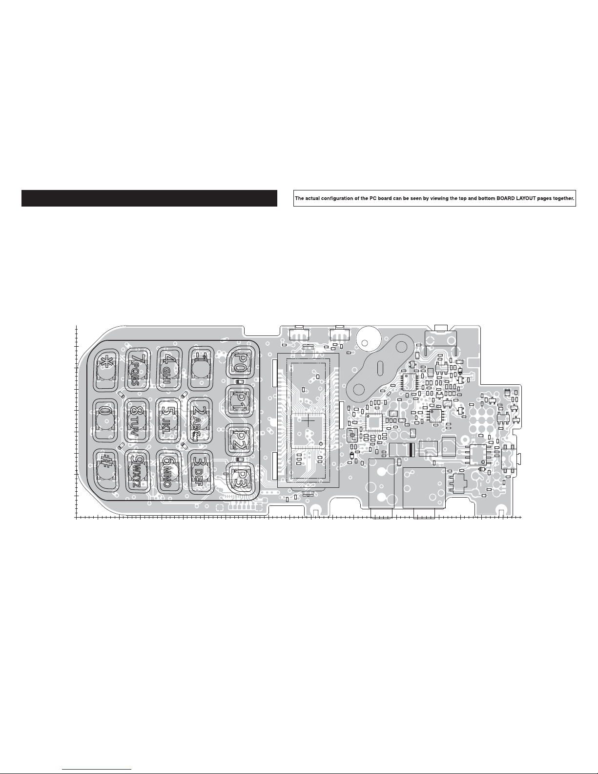
* Depending on the transceiver version.
[UP]/[Upper]*[DOWN]/[Lower]*
8-1
SECTION 8
SECTION 8 BOARD LAYOUTS
• MAIN UNIT (B-8116B)
(TOP VIEW)
[PTT]
C2
C3
C8
C9
C11
C14
C16
C18
C19
C20
C21
C24
C25
C26
C27
C29
C32
C33
C36
C38
C39
C41
C47
C52
C65
C66
C67
C70
C74
C79
C89
C90
C91
C92
C93
C94
C95
C96
C98
C99
C103
C105
C114
C115
C118
C119
C120
C121
C259
C272
C290
C309
C316
C317
C318
C320
C334
C335
C336
C337
C354
C356
C374
C375
C378
C380
C381
C384
C385
C389
C391
C407
C412
C417
C419
C420
C422
C423
C424
C425
C434
C437
C438
C440
CP21
D1
D4
D5
D20
D34
D35
DS1
DS3
DS4
DS5
DS6
DS7
DS8DS9
DS10
EP2
EP3
EP18
EP19
EP21
F1
IC1
IC2
IC3
IC4
IC17
IC19
IC21
J1
J2
J3
MC1
MP5
Q2
Q3
Q9
Q15
Q16
Q21
Q22
Q40
R3
R4
R6
R8
R10
R11
R14
R15
R16
R17
R18
R19
R35
R41
R56
R58
R69
R70
R72
R86
R87
R88
R89
R91
R137
R138
R155
R157
R220
R221
R222
R232
R233
R234
R235
R247
R271
R282
R283
R292
R294
R296
R298
R299
R311
R322
R332
R333
R334
R338
R339
R340
R341
R347
R348
S1
S2S3
S5
S6
S7
S8
S9
S10
S11
S12
S13
S14
S15
S16
S17
S18
S19
S20
S21
X1
B-8116B
H0H5H10H15H20H25H30H35H40H45H50H55H60H65H70H75H80H85H90H95H100
V0 V5 V10 V15 V20 V25 V30 V35 V40
Page 31

8-2
• MAIN UNIT (B-8116B)
(BOTTOM VIEW)
[ROTARY SELECTOR]
[VOL]
MC1
J2
C1
C4
C5
C6
C7
C10
C12
C13
C15
C22
C23
C28
C34
C35
C40
C43
C44
C45
C48
C49
C53
C54
C56
C58
C61
C63
C73
C77
C82
C83
C84
C85
C86
C87
C97
C100
C104
C106
C108
C109
C110
C112
C113
C116
C124
C125
C126
C127
C128
C129
C130
C131
C132
C133
C134
C135
C136
C137
C138
C140
C141
C142
C143
C144
C145
C146
C147
C150
C151
C152
C153
C154
C157
C158
C159
C161
C162
C165
C167
C168
C169
C170
C171
C173
C175
C176
C177
C178
C180
C183
C184
C186
C187
C188
C189
C191
C192
C194
C195
C196
C197
C198
C199
C200
C201
C202
C203
C204
C205
C206
C207
C208
C210
C212
C213
C214
C215
C216
C217
C218
C219
C221
C223
C224
C225
C227
C231
C233
C234
C235
C236
C237
C238
C239
C240
C241
C242
C243
C244
C245
C246
C247
C248
C250
C251
C252
C253
C254
C256
C257
C258
C260
C261
C262
C263
C264
C265
C267
C268
C269
C271
C274C275
C276
C277
C278
C279
C280
C281
C282
C283
C284
C285
C288
C289
C293
C294
C296
C297
C300
C301
C303
C305
C306
C307
C308
C310
C311
C313
C314
C315
C319
C321
C323
C324
C325
C326
C328
C330
C331
C332
C333
C338
C339
C341
C343
C344
C345
C346
C347
C348
C349
C350
C352
C353
C355
C357
C360
C361
C362
C363
C364
C365
C366
C369
C377
C379
C382
C383
C386
C388
C390
C392
C393
C394
C395
C396
C397
C398
C399
C400
C403
C405
C408
C409
C410
C411
C413
C414
C415
C418
C421
C432
C433
C436
C441
D6
D7
D9
D10
D11
D12
D13
D16
D17
D18
D19
D22
D23
D24
D25
D27
D28
D29
D31
D32
D33
D36
D37
D38
EP1
EP4
EP5
EP6
EP7
EP10
EP11
EP15
EP16
EP17
EP20
EP22
EP23
FI1
IC5
IC6
IC7
IC8
IC9
IC10
IC11
IC13
IC14
IC15
IC16
IC20
IC22
IC23
IC24
L2
L3
L5
L6
L7
L9
L10
L11
L13
L14
L15
L16
L17
L19
L21
L22
L23
L24
L25
L26
L27
L28
L29
L30
L31
L32
L33
L34
L35
L36
L37
L38
L39
L40
L41
L42
MP2
MP3
Q1
Q4
Q5
Q10
Q14
Q17
Q19
Q20
Q23
Q24
Q25
Q27
Q28
Q29
Q30
Q31
Q32
Q33
Q34
Q36
Q37
Q38
Q39
Q41
Q42
Q44
R1
R2
R5
R12
R13
R20
R21
R22
R24
R25
R26
R27
R28 R29
R30
R31
R42
R43
R47
R48
R49
R50
R52
R53
R55
R59
R60
R61
R62
R64
R65
R66
R67
R68
R81
R83
R84
R85
R90
R92
R93
R94
R95
R96
R97
R98
R99
R100
R101
R102
R103
R104
R105
R106
R107
R110
R112
R113
R115
R116
R117
R119
R122
R123
R124
R125
R126
R130
R131
R140
R143
R144
R145
R146
R147
R150
R151
R152
R153
R156
R158
R159
R160
R162
R163
R164
R165
R166
R167
R168
R169
R170
R173
R176
R177
R178
R179
R181
R182
R183
R184
R185
R186
R187
R188
R190
R191
R192
R193
R194
R196
R197
R198
R199
R200
R201
R202
R203
R204
R205
R206
R207
R208
R209
R210
R211
R212
R213
R214
R215
R216
R217
R218
R219
R223
R224
R225
R227
R228
R229
R236
R237
R238
R239
R240
R241
R243
R244
R245
R246
R248
R249
R250
R251
R253
R254
R256
R257
R258
R259
R260
R263
R264
R265
R266
R267
R268
R269
R270
R272
R273
R274
R275
R276
R277
R278
R279
R280
R284
R286
R287
R288
R289
R290
R291
R295
R297
R300
R301
R302
R303
R304
R305
R307
R308
R309
R310
R312
R313
R314
R317
R319
R320
R323
R324
R325
R326
R327
R328
R329
R330
R331
R335
R336
R337
R342
R345
R346
R349
R350
R351
R352
S4
X2
X3
H0
H5
H10
H15 H20
H25
H30 H35
H40 H45
H50
H55
H60 H65
H70
H75 H80
H85 H90
H95 H100
V0V5V10V15V20V25V30V35V40
Page 32

• For #01, #04, #05, #08, #09, #12 and #13
9-1
SECTION 9. BLOCK DIAGRAM
LPF
PWR
DET
D22
D23
MUTE
SW
Q40
ANT
SW
D27
D19
PWR
AMP
Q38
RD07MUS2B
TX/RX
SW
D16
D17
Q25
D9,D32
Q27
D33,D12
FIL
RIPPLE
Q23
2SC4116
VCO
SW
Q29:LDTC144EEQ29
FIL
LOOP
PLL
IC
IC15
AK1542
FM
MOD
D13
1SV309
Q37
3SK293
BPF
RF
AMP
Q39
APC
AMP
IC17
TA75S01F
BPF
XTAL
FI1
FL-442
IF
AMP
Q33
2SC4215
BUFF
Q31
2SC5107
BUFF
Q30
2SC5107
BUFF
Q32
2SC5107
DRIVE
AMP
Q36
RD01MUS1
X3
CR-794
TCXO
LV
ADJ
D11
LV
ADJ
D10
BUFF
IC7
NJM12902
VOL1
R133
PRE
AMP
Q34
2SC5107
VCO
SW
Q28
BPF
D29
HVB350B
BPF
D25
HVB350B
BPF
D31
HVB350B
F1
ERBSE3R00U
12
PTT
DET
Q3
AF
AMP
IC1 TPA0211DGN
J2
LPF
LM2902
IC7
T5
REG
Q17
SP1
VOL1
R133
REG
+5V
IC20
LED
CTRL
Q21:Q22
REG
S5
Q15
BATTERY_1
BT1
R155
SHIFT
SW
D6
AF VOL
R1
PUSH1
PTT
PUSH1
P2
EEPROM
IC13
MC1
EM9745P
LPF
DMG504010
Q5
D7
Q20
CLONE
BUFF
PWR
CTRL
Q9
Q10
AF
AMP
IC12
TA7368F
LPF
IC5
LM2902
J3
1
2
DET
D5
SELECT
S4
CH
RESET
IC8
SW
FIL
Q19
SW12
S5
LPF
IC11
NJM12902
VOL1
R132
REG
R5
Q16
PUSH1
P1
J1
X2
CR-864
AUTO_TX
CTRL
Q1
AMP
NLM12902
IC3
LPF
HR
YG
DS1
CL-165HR
BPF
D18
HVB350B
LPF
IC11
NJM12902
VOL1
R133
IC23
CONV
LCD
DRIVER
IC21
IC21
IC21
LCD
DS2
DS2
VOL1
R133
VOL1
R133
VOL1
R133
VOL1
R133
AMPLPFAMP
AMP
LIMIT
AMP
DS3,DS4
DS5,DS6
DS4
TC4S66F
IC14
BPF
D28
HVB350B
14.7456MHz
X1
MIC
GAIN
IC2
DS7,DS8
DS3
DS9,DS10
DS4
LED
CTRL
Q41
IC22
CPU5
REG
IC6
+3V
REG
IC24
HPF
REG
+5V
IC19
D/A
IF IC
LVIN
S5V
R5V
RX VCO
TX VCO
T2 T1
T1
TMUT
IC16
REF
BAL
15.3MHz
45.9MHz
DISC
SQIN
46.35MHz
MAIN UNIT
MIXER
LV
LVA
136-174MHz
182.35MHz-220.35MHz
R5C
VCON
CONTROL LINE
VOXV
F1
S5C
VCC
COMMON LINE
R5C
MOD
ATX
+5V
TX LINE
12.288MHz
T5C
BEEP
S5V
RX LINE
IC9
EPTT
AFVI
CPU
CSFT
R5V
CPU5
DATA LINE
F2
CDEC
DUSE
DISC
IC10
RES
Explanatory notes
AFON
CTCSS/DTCS DEC
PWOFFCENC1 (PWM)
TEMP
IPTT
CTCSS/DTCS
SENC
VCC
VCC
CPU5
S5V
T5V
RSSI NOIS
KEY1
KEY2
AFO AFO
MSK
FM/PM
LVIN
RSSI
NDIS
SDEC
VOXV
EPTT
DTMF/5TONE
/SUM
LVA
T1
T2
LIGHT
SENSOR
REF
KEY
MATRIX
EMPHEXP
SCRM
EMPH
COMP
SPLT
SDEC
HPF
HPF
MSK
Mod
MSK
De-Mod
IC2
IC4
+5V
S6-S21
MGC0
MGC1
Page 33

• For #02, #03, #06, #07, #10 and #11
LPF
PWR
DET
D22
D23
MUTE
SW
Q40
ANT
SW
D27
D19
PWR
AMP
Q38
RD07MUS2B
TX/RX
SW
D16
D17
Q25
D9,D32
Q27
D33,D12
FIL
RIPPLE
Q23
2SC4116
VCO
SW
Q29:LDTC144EEQ29
FIL
LOOP
PLL
IC
IC15AK1542
FM
MOD
D13
1SV309
Q37
3SK293
BPF
RF
AMP
Q39
APC
AMP
IC17
TA75S01F
BPF
XTAL
FI1
FL-442
IF
AMP
Q33
2SC4215
BUFF
Q31
2SC5107
BUFF
Q30
2SC5107
BUFF
Q32
2SC5107
DRIVE
AMP
Q36
RD01MUS1
X3
CR-794
TCXO
LV
ADJ
D11
LV
ADJ
D10
BUFF
IC7
NJM12902
VOL1
R133
PRE
AMP
Q34
2SC5107
VCO
SW
Q28
BPF
D29
HVB350B
BPF
D25
HVB350B
BPF
D31
HVB350B
F1
ERBSE3R00U
12
PTT
DET
Q3
AF
AMP
IC1 TPA0211DGN
J2
LPF
LM2902
IC7
T5
REG
Q17
SP1
VOL1
R133
REG
+5V
IC20
LED
CTRL
Q21:Q22
REG
S5
Q15
BATTERY_1
BT1
R155
SHIFT
SW
D6
AF VOL
R1
PUSH1
PTT
PUSH1
P2
EEPROM
IC13
MC1
EM9745P
LPF
DMG504010
Q5
D7
Q20
CLONE
BUFF
PWR
CTRL
Q9
Q10
AF
AMP
IC12
TA7368F
LPF
IC5
LM2902
J3
1
2
DET
D5
SELECT
S4
CH
RESET
IC8
SW
FIL
Q19
SW12
S5
LPF
IC11
NJM12902
VOL1
R132
REG
R5
Q16
PUSH1
P1
J1
X2
CR-864
AUTO_TX
CTRL
Q1
AMP
NLM12902
IC3
LPF
HR
YG
DS1
CL-165HR
BPF
D18
HVB350B
LPF
IC11
NJM12902
VOL1
R133
IC23
LCD
DRIVER
IC21
LCD
DS2
DS2
VOL1
R133
VOL1
R133
VOL1
R133
VOL1
R133
AMPLPFAMP
AMP
LIMIT
AMP
DS3,DS4
DS3
DS5,DS6
DS4
TC4S66F
IC14
BPF
D28
HVB350B
14.7456MHz
X1
MIC
GAIN
IC2
DS7,DS8
DS3
DS9,DS10
DS4
LED
CTRL
Q41
IC22
CPU5
REG
IC6
+3V
REG
IC24
REG
+5V
IC19
LPF
D/A
IF IC
LVIN
S5V
R5V
RX VCO
TX VCO
T2 T1
T1
TMUT
IC16
REF
BAL
15.3MHz
45.9MHz
DISC
SQIN
46.35MHz
MAIN UNIT
MIXER
LV
LVA
136-174MHz
182.35MHz-220.35MHz
R5C
VCON
CONTROL LINE
VOXV
F1
S5C
VCC
COMMON LINE
R5C
MOD
ATX
+5V
TX LINE
12.288MHz
T5C
BEEP
S5V
RX LINE
IC9
EPTT
AFVI
CPU
CSFT
R5V
CPU5
DATA LINE
F2
CDEC
DUSE
DISC
IC10
RES
Explanatory notes
AFON
CTCSS/DTCS DEC
PWOFFCENC1 (PWM)
TEMP
IPTT
CTCSS/DTCS
SENC
VCC
VCC
CPU5
S5V
T5V
RSSI NOIS
KEY1
KEY2
AFO AFO
MSK
FM/PM
LVIN
RSSI
NDIS
SDEC
VOXV
EPTT
DTMF/5TONE
/SUM
LVA
T1
T2
LIGHT
SENSOR
REF
KEY
MATRIX
EMPHEXP
SCRM
EMPH
COMP
SPLT
SDEC
HPF
HPF
MSK
Mod
MSK
De-Mod
IC2
IC4
+5V
CONV
S6-S21
MGC0
MGC1
,D36,D37,D38
9-2
Page 34

10-1
SECTION 10. VOLTAGE DIAGRAM
*: Refer to the PARTS LIST for the value and name of component.
• MAIN UNIT (1/3)
R234
10k
R176
100
R146
1k
Q39
3SK293
R178
560
R181
47
R156
10k
R145
10k
Q23
2SC4116
R238
10
*Q14
150k
R151
*R249
CP9
R202
10k
ANT_BOARD
4.7k
R219
R197
10k
*R239
R170
4.7
MMZ1005Y102CTEP5
R153
1k
MMZ1005Y102CT
EP4
TA75S01F
IC17
1
2
3
4
5
R227
100k
MMZ1005Y102CT
EP7
R159
100k
R220
10
HV
+5V
S5V
R5V
T5V
SO
SCK
PLST
Q37
3SK293
LVIN
DISC
NOIS
NWC
TMUT
MOD
VCON
SQIN
LVA
T1
T2
UNLK
RSSI
R186
470
R5C
R233
120k
R203
47
R224
47
100k
R215
68k
R251
OG-503040
MP2
1k
R228
R165
1k
LDTA144EE
Q40
*D24
R191
10
LDTC144EE
Q24
R212
3.3k
R164
680k
0.5P
C353
0.001
C354
0.001
C332
0.001
C331
0.001
C279
0.001
C283
0.001
C356
0.001
C335
0.001
C337
0.001
C316
0.001
C317
0.01
C318
0.001
C289
10P
C253
47P
C262
0.001
C261
0.001
C263
0.001
C252
0.001
C251
0.001
C248
0.001
C225
0.001
C256
3P
C254
0.1
C223
0.75P
C224
0.001
C219
0.001
C200
0.01
C168
0.001
C165
0.001
C170
47P
C171
47P
C178
47P
C177
0.1
C162
0.001
C175
0.001
C173
0.001
C196
*C357
0.001
C320
0.001
C319
0.001
C339
0.001
C341
0.001
C366
0.001
C364
0.1
C324
*C296
0.001
C271
0.001
C272
0.001
C297
0.001
C267
0.01
C274
0.01
C269
0.01
C259
0.01
C277
100P
C258
0.001
C244
330P
C245
0.001
C239
1
C236
6P
C215
56P
C216
56P
C214
0.01
C213
0.01
C212
0.01
C180
0.001
C161
0.1
C176
1
C189
*C338
10P
C198
*C275
0.5P
C227
R194
2.2k
R196
100k
10
C243
220k
R160
L9
0.18U
L10
0.18U
R163
56
1M
R185
220k
R184
0.001
C240
R183
47k
47P
C218
100P
C217
100P
C238
1
C237
0.22
C235
0.1
C233
4.7k
R143
0.001
C169
1 C195
27k
R162
0.22
C199
0.22
C260
TC7W66FU
IC14
5
6
3
TC7W66FU
IC14
1
2
7
TC7W66FU
IC14
V+
8
GND
4
10
C184
0
R253
0
R254
10
C234
RD01MUS2B
Q36
1k
R173
BAR88
D19
D16
BAR88
D27
BAR88
100k
R257
BAR88
D28
0.22
C197
Q31
2SC5108
Q32
2SC5108
Q34
2SC5108
D18
1SV305
1SV305
D29
R187
10k
L16
39N
0.001
C265
R207
2.2k
100P
C282
68
R209
0.01
C288
22N
L19
MMZ1005Y102CT
EP6
0.001
C305
1
C284
0.001
C309
1
C307
47P
C308
0.001
C301
68P
C306
22
R218
0.001
C314
100k
R211
*L23
0.5P
C355
10k
R244
6.8k
R243
RB876W
D23
RB876W
D22
4.7U
L27
45.3N
L26
4.7kR245
4.7kR246
45.5N
L29
45.3N
L30
27.2N
L31
15P
C333
1.5P
C348
4P
C349
27P
C350
24P
C352
18P
C303
22P
C330
0.001
C310
0.001
C315
R247
10k
R232
220k
R235
68k
11P
C369
L34
45.3N
15P
C365
6P
C363
L33
82N
6P
C362
L32
68N
1.5P
C346
L28
68N
3.5P
C345
100P
C344
100P
C360
R241
4.7k
R250
4.7k
R236
100k
18k
R237
220k
R1
R240
120k
L24
LQW18AN56NG00
0.001
C281
L25
LQW18AN56NG00
4P
C326
0.001
C325
*C321
1.5P
C323
5P
C300
6P
C280
R217
82k
R216
68
120k
R214
150k
R213
*R20
R199
1k
D17
BAR88
R229
270
4.7
R24
L14
0.1U
R190
47k
7P
C250
0.001
C285
R192
10
L15
0.1U
R193
47k
10P
C257
33N
L11
12P
C210
12P
C231
*L13
R177
120k
R168
1.8k
R169
1.8k
R167
3.9k
R166
3.9k
33P
C208
33P
C187
L6
68N
33N
L36
10U
L2
3.3U
L5
0.33
C183
68P
C206
33P
C205
1P
C194
L7
82N
10U
L37
68N
L38
3.3U
L39
47P
C381
R144
1.2k
2.2
C167
0.33
C28
FSIO
FSCN
L1SS400
D20
1
C290
+3_3V
FSCK
RSTN
47k
R21
0.001
C13
470P
C247
27P
C203
27P
C204
24P
C207
33P
C188
4P
C15
4P
C35
47P
C186
27P
C202
MMZ1005A152ET
EP15
MMZ1005A152ET
EP16
0.001
C154
BBY57
D11
1SV323
D32
D9
1SV323
1SV323
D33
D12
1SV323
BBY57
D10
D13
1SV323
R179
470
Q29
LDTC114YE
LDTC114YE
Q28
1U
L3
0.001
C422
0.001
C436
100k
R150
0.001
C410
0.001
C221
0.1
C153
R198
4.7k
47
R337
470P
C421
47
R336
RD07MUS2B
Q38
0.001
C336
100P
C390
10
C415
33k
R338
BBY57
D31
D2
5
BBY57
3621MP3
123
4
3621
MP5
Q25
2SC4226
Q27
2SC4226
AK1542A
IC15
1
CPVDD
2
TEST3
3
TEST1
4
LE
5
DATA
6
CLK
7LD8
PDN29PDN110REFIN11TEST212GPO1
13
GPO2
14
DVSS
15
VREF
16
RFINN
17
RFINP
18
PVDD
19
BIAS20PVSS
21CP22
CPZ
23
SWIN
24
25
CR-978
X3
1VC2
GND
3
OUT4VCC
Q30
2SC5108
1k
R331
0.001
C48
0.001
C49
MMZ1005A152ET
EP17
R206
180
0.001
C361
7P
C40
4P
C201
6P
C152
6P
C151
1P
C403
1
C425
*C328
0.22
C334
16.1N
L22
*L40
470P
C191
0.0015
C192
R182 180k
R188
1.5k
150P
C241
150P
C242
R147
39k
R152
27k
33k
R208
0.001
C268 *C293
*L21
3.5P
C343
0
R349
680
R223
R158
2.2k
SC-1451A
IC16
1
IFIP
2
NC
3
NC
4
NC
5
NC
6
VREFA
7
AVSS
8
AVDD
9
BIAS10NRECTO11NAMPO12NAMPI13AUDIOOUT14DISCOUT15PDOUT16RSSIOUT
17
IFOUT
18
AVSS2
19
PDN
20
RSTN
21
CSN
22
SCLK
23
SDATA
24
DETO
25
DVDD26DVSS
27
VREFD28AVSS3
29
AGNDOUT
30
AGNDIN
31
LOCAP
32
LOIN
33
MPZ1608S221A
EP10
*C405
15P
C313
1.2k
R221
*R350
*Q33
*R205
*C276
*C278
*R204
*FI1
1
IN
2
OUT3GND
4
GND
56
*L17
*C294
*D36
*D37
*D38
*R225
*R248
*R22
*R210
*R256
*C264
*R201 *R200
*L35
*R351
*C311
*C347
*R352
*C441
*L42
*C246
*L41
*R222
HV
+5V
S5V
R5V
T5V
SO
SCK
PLST
NWC
TMUT
MOD
VCON
SQIN
LVA
T1
T2
LVIN
DISC
NOIS
MOD
RSSI
LVA
R5C
T1
RSSI
HV
T2
T1
UNLK
R5C
R5C
S5V
SQIN
SCK
SO
PLST
GP01
LVIN
GP01
S5V
UNLK
S5V
FSIO
FSCN
T5V
DISC
T5V
PAV
FSIO
FSCN
+3_3V
+3_3V
RSTN
FSCK
FSCK
RSTN
GP02
GP02
RSSI
NWC
APCV
+5V
TMUT
NOIS
VCON
T1
R5V
R5V
+5V
+5V
R5V
X3 MULTI
T5V
TX VCO
APC
S5V
RX VCO
T5V
LPF
IF AMP
AGC
VCOV
HV
IF IC
RF AMP
T5V
MIX
HV
R5C
R5V
PLL
Page 35

10-2
• MAIN UNIT (2/3)
*: Refer to the PARTS LIST for the value and name of component.
RSTN
AFON
1
C91
470
R284
0.001
C39
2SB1132L
Q9
1k
R6
AK2346A
IC4
1
MSKCLK2DIO3SCLK4DIR5XOUT6XIN
7
DVDD
8
VSS1
9
AVDD
10
RXIN
11
RXINO
12
FILTERO
13
RXOUT
14
AGNDIN
15
AGND
16
EXTIN117EXTINO
18
VSS2
19
TXIN
20
TXINO
21
EXTIN2
22
MOD
23
RSTN
24
MSKDATA
25
CENC1
NWC
1
C90
J1
68k
R55
0.001
C41
1k
R25
PWOFF
AUTX
LDTC144EE
Q42
470
R97
LDTC144EE
Q4
S5C
FSIO
0.001
C105
T5C
FSIO
100k
R14
DTA113ZE
Q17
0.001
C74
R5C
FSCK
LDTC144EE
Q2
SO
15k
R324
68k
R68
R49
82k
0.01
C99
L1SS400
D4
PLST
FSCK
CL
R50
470
0.01
C103
NWC
FSCN
68k
R83
PMFM
47k
R66
6.8k
R29
0.1
C97
4.7k
R81
FSCN
68k
R65
0.0068
C44
0.1
C73
470
R18
MDIO
PLST
R5C
0.001
C10
0.1
C82
3.3k
R30
0.01
C115
MSCK
47k
R52
+5V
T5V
0.01
C135
0.018
C83
1
C34
MDIR
33k
R2
TC74VHC4066AFK
IC2
1
I/O1
2
O/I1
3
O/I2
4
I/O2
5
CONT2
6
CONT3
7
VSS8I/O3
9
O/I3
10
O/I4
11
I/O4
12
CONT4
13
CONT1
14
VDD
47k
R84
0.0012
C86
1M
R72
47k
R64
47k
R11
MGC0
47k
R10
MGC1
1
C61
10
C26
0.1
C112
XC6209F502MR
IC19
1
VIN
2
VSS
3
CE4NC
5
VOUT
47P
C93
680P
C84
TMUT
R126
180k
10
C1
LDTA114EE
Q16
47P
C94
MOD
DUSE
1
C100
47P
C95
LDTC144EE
Q1
EPTT
NOIS
J3
1
2
34
RSSI
1
C79
0.01
C98
6.8k
R53
47P
C92
VCON
CDEC
470P
C52
47P
C157
XC6209F502MR
IC20
1
VIN
2
VSS
3
CE4NC
5
VOUT
MMZ1005Y102CT
EP3
1M
R58
SDEC
LVA
1
C375
0.1
C70
0.1
C147
MMZ1005Y102CT
EP2
AFVI
3621
EP11
12
34
0.1
C132
1
C118
10k
R85
0.1
C131
MTDT
1C119
10k
R48
0.01
C130
MTCK
0.1C120
DRA9123Y0
Q3
100k
R19
0.001
C5
0.001
C6
NOIS
0.1C121
DMG504010
Q5
1
2
3
4
5
6
0.001
C4
47P
C14
0.1
C54
UNLK
56k
R47
DMC506010R
Q10
123
456
0.001
C9
0.001
C150
ERBRE3R00V
F1
12
0.1
C25
TMUT
47P
C36
0.001
C158
VCC
10k
R88
EZJZ0V80010
D1
LDTC144EE
Q19
R12
22k
R116
270k
100k
R87
100k
R157
100
R5
0.1
C384
DISC
0.1
C116
AK2330
IC10
1
VIN72VIN0
3
VOUT04VOUT1
5
VIN16RSTN
7
CSN
8
SCLK
9
SDATA
10
DVDD
11
VSS
12
AVDD
13
VREF14VIN215VOUT216VOUT317VIN318VIN4
19
VOUT4
20
VOUT5
21
VIN5
22
VIN6
23
VOUT6
24
VOUT7
25
ERTJ0EP473J
R155
0.1
C385
0
R96
10
C129
TEMP
*EP1
47P
C12
SQIN
LVIN T1
0.001
C16
T2
UNLK
1
C24
0.1
C22
0.1
C66
RB706F
D5
VOXV
1k
R95
0.1
C32
SCK
10
C45
0.039
C23
0.001
C47
BEEP
HV
68k
R67
R31
390k
DAST
0.1
C43
SENC
R28
22k
0.1
C56
LVIN
J2
0.022
C63
68k
R86
+5V
S5V
ISD8102SYI
IC1
1
Shutdown
2
VREF
3
MODE
4
VIN
5
VOUTP
6
VDD
7
GND
8
VOUTN
9
0.001
C2
68kR99
R5V
1
C58
0.001
C3
22
C159
0.001
C77
SO
100P
C133
0.1
C380
1k
R42
RSSI
SCK
R125
470k
R13
22k
0.001
C19
0.001
C414
0.001
C400
0.0022
C391
220P
C114
0.001
C407
47P
C408
0.001
C412
0.1
C434
0.001
C417
0.001
C424
0.47
C33
0.001
C411
0.001
C418
0.1
C419
10k
R333
330
R332
100k
R335
27k
R330
470
R70
680k
R69
R124
82k
1k
R41
NJM2904CRB1
IC7
2
3
1
NJM2904CRB1
IC7
6
5
7
NJM2904CRB1
IC7
V+
8
GND
4
NJM2904CRB1
IC5
V+
8
GND
4
NJM2904CRB1
IC3
V+
8
GND
4
NJM2904CRB1
IC11
V+
8
GND
4
NJM2904CRB1
IC3
2
3
1
NJM2904CRB1
IC3
6
5
7
NJM2904CRB1
IC5
6
5
7
NJM2904CRB1
IC5
2
3
1
NJM2904CRB1
IC11
6
5
7
NJM2904CRB1
IC11
2
3
1
CR-980
X1
DTA113ZE
Q15
1k
R15
1.8M
R35
180k
R101
330P
C134
22k
R339
12k
R340
1SS390
D34
0.1
C438
12k
R341
CSFT
0.001
C423
100k
R89
0.033
C65
220k
R100
R122
180k
R123
100k
15k
R130
8.2k
R131
5.6k
R56
10k
R16
5.6k
R17
47k
R26
3.9k
R43
6.8k
R342
R08717NSFK150S070A103
R27
0.047
C27
0.033
C67
82P
C89
1
C440
EZJZ0V80010
D35
0.22
R8
10k
R345
1.2k
R61
100k
R346
10P
C96
47P
C437
1kR91
1k
R348
0.1
C113
680P
C85
270P
C87
0.0033
C109
120P
C110
1.8MR90
8.2k
R334
0.01
C420
180k
R102
270kR98
*EP18
*EP19
*EP20
*EP23
220
R3
2k
R4
220
C29
*EP22
*EP21
*C53
*R347
*MC1
MDIO
DISC
FSCN
FSCN
FSCK
+5V
FSCK
FSIO
FSIO
MSCK
AUTX
MDIO
NWC
AFON
MTCK
SCK
SO
CL
BAL
SQIN
R5V
MDIR
AFON
MGC1
VREF
CDEC
DAST
PLST
R5C
T5C
VCON
S5C
PWOFF
DAST
CENC1
SCK
RSTN
SO
AFVIAFVI
DISC
VCC
REF
MOD
R5C
UNLK
S5V
LVIN
VCC
S5V
UNLK
T5V
NOIS
MTCK
RSTN
MTDT
RSTN
NOIS
+5V
+5V
R5C
TMUT
PMFM
T5V
SCK
CL
S5V
T2
S5V
S5V
VCON
MTDT
VOXV
NWC
CENC1
LVA
PLST
AFO
SENC
+5V
SENC
BEEP
VOXV
RSSI
LVIN
TEMP
DISC
MOD
DISC
AFO
SO
TEMP
SQIN
AFVI
SDEC
T1
CDEC
RSSI
EPTT
DUSE
TMUT
R5V
MGC1
DUSE
MGC0
T2
BEEP
MDIR
SDEC
MSCK
T1
LVA
VREF
VREF
+5V
+5V
PMFM
+5V+5V
T5C
PWOFF
+5V
AUTX
CSFT
CSFT
+5V
EPTT
S5C
B
A
B
A
+5V
VREF
CL
EPTT
ATX
CTCSS/DTCS FILTER
B
B
A
A
Page 36

10-3
• MAIN UNIT (3/3)
*: Refer to the PARTS LIST for the value and name of component.
1M
R92
*S11
CP3
OPT2
100k
R303
0.1
C142
*S6
BEEP
100k
R286
100k
R308
0.027
C124
*DS5
SENC
CP11
DCLK
100k
R307
*DS8
12k
R104
100k
R287
*S9
CP4
DCS
100k
R309
*S19
22
C141
CP12
DAT0
100k
R310
*S8
1SS390
D6
+5V
CP15
DAT1
100k
R311
*S13
10k
R105
*R282
CP13
DAT2
*S21
*R283
CP14
DAT3
*R323
100k
R312
*S16
10
R93
CP16
P87
100k
R313
*DS10
*C378
CP17
P86
100k
R314
*DS7
100k
R288
*Q44
100k
R319
*S10
100k
R59
1k
R272
FSIO
*S7
12k
R94
100k
R320
1kR276
*S12
CL
1
C386
100k
R317
0.001
C21
FSCK
*DS9
22k
R103
100k
R289
0.001
C7
1kR277
*S18
1
C145
100k
R290
LDTA144EE
Q21
FSCN
*S20
J4
1
2
3
4
5
6
7
8
9
10
11
12
13
14
1516
1kR278
*S15
PMFM
0.1
C143
RSSI
0.001
C136
HR
YG
CL-165HR
DS1
RSTN
MDIO
0.001
C20
*S17
MTDT
15k
R291
4.7k
R325
CENC1
0.001
C38
*IC21
1
COM1
2
COM2
3
COM3
4
COM4
5
SEG1
6
SEG2
7
SEG3
8
SEG4
9
SEG5
10
SEG6
11
SEG7
12
SEG8
13
SEG9
14
SEG10
15
SEG11
16
SEG12
17
SEG1318SEG1419SEG1520SEG1621SEG1722SEG1823SEG1924SEG2025SEG2126SEG2227SEG2328SEG2429SEG2530SEG2631SEG2732SEG28
33
SEG29
34
SEG30
35
SEG31
36
SEG32
37
SEG33
38
SEG34
39
SEG35
40
SEG36
41
SEG37
42
SEG38
43
SEG39
44
SEG40
45
SEG41
46
SEG42
47
SEG43
48
SEG44
49
SEG4550SEG4651SEG4752SEG4853SEG4954SEG5055VLCD056INHb57SCL58DATA59CE60MODE61VSS62OSC163OSC264VDD
*DS6
1kR258
4.7k
R107
4.7k
R326
SW-149
S1
1k
R263
MSCK
*R271
0.001
C18
*S14
1k
R259
XC6221A302MR
IC24
1
VIN
2
VSS
3CE4
NC
5
VOUT
390
R137
1k
R264
1k
R280
*IC22
1
IOVdd
2
DNC
3
DNC
4
GND6RES
7
INT
8
ADDR
9
SCL
5
Vdd
10
SDA
MTCK
0.01
C146
0R295
*C388
LDTA144EE
Q22
1k
R265
MDIR
1kR260
0.001
C138
EVQ-PUL
S5
1k
R266
MGC0
R4F20335RDFE
IC9
1
PB6/AN6/DA0
2
PB7/AN7/DA1
3
AVCC
4
AVref
5
X2
6
X1
7
RES
8
TEST
9
Vss
10
PJ1/OSC2/CLKOUT
11
PJ0/OSC1
12
VCC
13
NMI
14
P87/TREO
15
P86/TRBO
16
P85/TRAIO
17
P84/TRGB
18
P83/TRAO
19
P82
20
P81
21
P80
22
P37/TXD_X/TXDX/RXDX
23
P36/RXD_X/RXDX
24
P35/SCK3_X
25
P34/FTCI
26
P33/FTIOD27P32/FTIOC28P31/FTIOB29P30/FTIOA/TRGC30P14/IRQ431P15/IRQ532P16/IRQ633P17/IRQ734P57/SCL/SSI35P56/SDA/SCS36P55/SSCK37P54/SSO38P53/TGIOB39P52/TGIOA40P51/TCLKB41P50/TCLKA42P10/IRQ043P11/IRQ144P27/TXD_245P26/RXD_246P4747P4648P4549P4450P43
51
P42
52
P41
53
P40
54
P25/SCK3_2
55
P60/FTIOA0
56
P61/FTIOB0
57
P62/FTIOC0
58
P63/FTIOD0
59
P64/FTIOA1
60
P65/FTIOB1
61
P66/FTIOC1
62
P67/FTIOD1
63
VSS
64
P24/TRDOI_0
65
P20/SCK3
66
P21/RXD
67
P22/TXD
68
P23/TRCOI
69
VCC
70
P12/IRQ2
71
P13/IRQ3
72
P94/FTIOA3
73
P95/FTIOB3
74
P96/FTIOC3
75
P72
76
P7377P7478P7579P7680P77
81
P97/FTIOD382P90/FTIOA283P91/FTIOB284P92/FTIOC285P93/FTIOD2
86
PA4/AN0_287PA5/AN1_288PA6/AN2_289PA7/AN3_2
90
PA0/AN891PA1/AN9
92
PA2/AN1093PA3/AN11
94
AVss
95
PB0/AN096PB1/AN197PB2/AN298PB3/AN399PB4/AN4
100
PB5/AN5
NOIS
0.1
C144
0.001
C382
100k
R296
*R327
PWOFF
MGC1
0.001
C374
UNLK
1k
R106
0.001
C383
*R297
+3_3V
1k
R273
1.8k
R138
S5C
0.01
C104
100k
R328
SO
T5C
TMUT
0.1
C108
*R300
*C389
1k
R274
R5C
XC6209F502MR
IC6
1
VIN
2
VSS
3
CE4NC
5
VOUT
100k
R62
*R299
SCK
100k
R140
PLST
DUSE
VCC
100k
R60
AFON
DAST
NWC
4.7k
R119
EPTT
1
C379
100k
R298
AUTX
4.7k
R115
CDEC
0.001
C8
GT24C128A
IC13
1
A0
2
A1
3
A2
4
VSS5SDA
6
SCL
7
WP
8
VCC
*R304
LRB706F
D7
0.1
C377
SDEC
0.001
C11
CF20OPEN
CP21
*R305
15k
R110
AFVI
0.1
C140
100k
R322
15k
R117
TEMP
CP7
NMI
*R301
DRC9144T0
Q20
LVIN
CP2
100k
R302
1k
R275
VOXV
CP10
OPT1
56k
R292
*Q41
*DS3
NJU7704F3
IC8
1
CD
2
VSS
3MR4
VOUT
5
VDD
CP6
P85
33k
R294
*DS4
CP5
RES
1
C106
0.001
C399
0.001
C413
0.001
C392
0.001
C393
1
C432
0.1
C433
1P
C126
0.001
C396
0.001
C397
0.001
C409
0.22
C128
0.001
C398
100k
R329
0R113
0R112
220
R279
0.001
C395
TAFG-12W
S2
TAFG-12W
S3
CR-981
X2
10P
C125
100P
C127
0.001
C394
CSFT
*R270
*R267
*R268
*R269
*DS2
24
SEG2423SEG2322SEG2221SEG2120SEG2019SEG1918SEG1817SEG1716SEG1615SEG1514SEG1413SEG1312SEG1211SEG1110SEG109SEG98SEG87SEG76SEG65SEG54SEG43SEG32SEG21SEG1
25
SEG3826SEG3727SEG3628SEG3529SEG3430SEG3331SEG3232SEG3133SEG3034SEG2935SEG2836SEG2737SEG2638SEG25
39
COM140COM241COM342COM4
ED08D13OFT176S065A
S4
1A12
C1
3
B1
4A25
C2
6
B2
7A38
C3
9
B3
0.01
C137
*IC23
1
VL
2
A1
3
A2
4
GND5OE
6
B2
7
B1
8
VH
SEG45
P87
SEG38
SEG44
BATV
SEG43
SEG37
SEG42
SEG36
+5V
SEG41
SEG35
SEG40
SEG34
IPTT
SEG39
SEG33
SEG38
SEG32
SEG37
ASCL
SEG31
KS0
SEG36
SEG30
SEG35
ASDA
SEG29
SEG34
SEG28
CBI0
KS1KS1
SEG33
SEG27
SEG32
CBI1
SEG26
SEG31
SEG25
CBI2
SEG30
SEG24
CBI3
SEG29
SEG23
SEG28
NMI
AINT
CPU5
SEG27
SEG26
SEG25
TLED
TEMP
SEG24
SEG18
DAST
SEG23
SEG17
BATV
PLST
SEG16
PLST
SEG15
R5C
SEG14
+5V
R5C
SEG13
+5V
T5C
SEG12
SEG11
+5V
S5C
SEG10
S5C
SEG9
PWOFF
SEG8
PWOFF
SEG7
SEG6
CPU5
SEG5
RSTN
SENC
CENC1
SENC
BEEP
VOXV
VOXV
COM4
LVIN
COM3
TEMP
COM2
AFVI
COM1
SDEC
IPTT
LSMD
EPTT
CDEC
LINH
CDEC
KRA
LIGT
EPTT
+3_3V
KR2
CPU5
RSSI
CL
+5V
P85
ASCL
DUSE
KR1
RES
ASDA
KR0
KS3
RES
KS2
P87
KS1
+5V
P86
KS0
CPU5
AINT
DUSE
TMUT
TMUT
RLED
TLED
CBI0
MGC1
RLED
MGC0
UNLK
MDIR
UNLK
CLI
NOIS
MSCK
CLO
MTCK
LVIN
MDIO
RSSI
FSCN
MTDT
AFVI
CPU5
FSCK
LINH
KR3
FSIO
CENC1
NWC
KR2
KR2
AFON
CL
DAST
AUTX
BEEP
NOIS
AUTX
NWC
FSCK
AFON
KR1
KR1
FSCN
SCK
SCK
FSIO
MDIR
SO
SO
KR0
KR0
MDIO
COM4
RSTN
SEG5
MTCK
LCS
SEG6
LSCK
SEG7
SDEC
LSO
MSCK
SEG8
MTDT
SEG9
LCS
SEG10
LSCK
COM1
SEG11
KS3
COM2
SEG12
LSO
COM3
SEG13
LSMD
SEG18
SEG14
LIGT
SEG15
P85
SEG16
SEG17
P86
SEG46
PMFM
CBI1
CBI2
CBI3
MGC1
MGC0
T5C
PMFM
NMI
KS2
+3_3V
+3_3V
KRA
CSFT
CSFT
CSFT
KR3
+5V
SEG45
SEG46
SEG39
SEG40
SEG41
SEG42
SEG43
SEG44
PTT
S1
S2
EMER
* 0 # P3
7 8 9 P2
4 5 6 P1
1 2 3 P0
Page 37

6F No.68, Sec. 1 Cheng-Teh Road, Taipei, Taiwan, R.O.C.
Phone : +886 (02) 2559 1899 Fax : +886 (02) 2559 1874
URL : http://www.asia-icom.com
E-mail : sales@asia-icom.com
Zac de la Plaine
1 Rue Brindejonc des Moulinais BP 5804
31505 Toulouse Cedex, France
Phone : +33 (5) 61 36 03 03 Fax : +33 (5) 61 36 03 00
URL : http://www.icom-france.com
E-mail : icom@icom-france.com
Blacksole House, Altira Park, Herne Bay, Kent CT6 6GZ, UK
Phone : +44 (0) 1227 741741 Fax : +44 (0) 1227 741742
URL : http://www.icomuk.co.uk
E-mail : info@icomuk.co.uk
Ctra. Rubi, No. 88 Bajos A 08174, Sant Cugat del Valles, Barcelona, Spain
Phone : +34 (93) 590 26 70 Fax : +34 (93) 589 04 46
URL : http://www.icomspain.com
E-mail : icom@icomspain.com
<Corporate Headquarters>
12421 Willows Road NE, Kirkland, WA 98034, U.S.A.
Phone : +1 (425) 454-8155 Fax : +1 (425) 454-1509
URL : http://www.icomamerica.com
E-mail : sales@icomamerica.com
<Customer Service>
Phone : +1 (425) 454-7619
Glenwood Centre #150-6165
Highway 17A Delta, B.C., V4K 5B8, Canada
Phone : +1 (604) 952-4266 Fax : +1 (604) 952-0090
URL : http://www.icomcanada.com
E-mail : info@icomcanada.com
Unit 1 / 103 Garden Road, Clayton VIC 3168 Australia
Phone : +61 (03) 9549-7500 Fax : +61 (03) 9549-7505
URL : http://www.icom.net.au
E-mail : sales@icom.net.au
No.101, Building 9, Caifuxingyuan Park, No.188 Maoting Road,
Chedun Town, Songjiang District, Shanghai, 201611, China
Phone : +86 (021) 6153 2768
Fax : +86 (021) 5765 9987
1-1-32, Kamiminami, Hirano-ku, Osaka 547-0003, Japan
Phone : +81 (06) 6793 5302
Fax : +81 (06) 6793 0013
URL : http://www.icom.co.jp/world/index.html
Communication Equipment
Auf der Krautweide 24
65812 Bad Soden am Taunus, Germany
Phone : +49 (6196) 76685-0
Fax : +49 (6196) 76685-50
URL
: http://www.icomeurope.com
E-mail : info@icomeurope.com
39C Rennie Drive, Airport Oaks,
Auckland, New Zealand
Phone : +64 (09) 274 4062 Fax : +64 (09) 274 4708
URL : http://www.icom.co.nz
E-mail : inquiries@icom.co.nz
Rua Itororó, 444 Padre Eustáquio Belo Horizonte MG,
CEP: 30720-450 Brazil
Phone : +55 (31) 3582 8847 Fax : +55 (31) 3582 8987
E-mail
: sales@icombrazil.com
Page 38

1-1-32, Kamiminami, Hirano-ku, Osaka 547-0003, Japan
S-15106XZ-C1
© 2014 Icom Inc.
 Loading...