

Page 1

PowerPC 405
Embedded Processor Core
User’s Manual
SA14-2339-04
Page 2

Fifth Edition (December 2001)
This edition of
IBM PPC405 Embedded Processor Core User’s Manual
applies to the IBM PPC405 32-bit
embedded processor core, until otherwise indicated in new versions or application notes.
The following paragraph does not apply to the United Kingdom or any country where such provisions
are inconsistent with local law: INTERNATIONAL BUSINESS MACHINES CORPORATION PROVIDES
THIS MANUAL “AS IS” WITHOUT WARRANTY OF ANY KIND, EITHER EXPRESSED OR IMPLIED,
INCLUDING, BUT NOT LIMITED TO, THE IMPLIED WARRANTIES OF MERCHANTABILITY AND FITNESS
FOR A PARTICULAR PURPOSE. Some states do not allow disclaimer of express or implied warranties in
certain transactions; therefore, this statement may not apply to you.
IBM does not warrant that the products in this publication, whether individually or as one or more groups, will
meet your requirements or that the publication or the accompanying product descriptions are error-free.
This publication could contain technical inaccuracies or typographical errors. Changes are periodically made to
the information herein; these changes will be incorporated in new editions of the publication. IBM may make
improvements and/or changes in the product(s) and/or program(s) described in this publication at any time.
It is possible that this publication may contain references to, or information about, IBM products (machines and
programs), programming, or services that are not announced in your country. Such references or information
must not be construed to mean that IBM intends to announce such IBM products, programming, or services in
your country. Any reference to an IBM licensed program in this publication is not intended to state or imply that
you can use only IBM’s licensed program. You can use any functionally equivalent program instead.
No part of this publication may be reproduced or distributed in any form or by any means, or stored in a data
base or retrieval system, without the written permission of IBM.
Requests for copies of this publication and for technical information about IBM products should be made to your
IBM Authorized Dealer or your IBM Marketing Representative.
Address technical queries about this product to ppcsupp@us.ibm.com
Address comments about this publication to:
IBM Corporation
Department YM5A
P.O. Box 12195
Research Triangle Park, NC 27709
IBM may use or distribute whatever information you supply in any way it believes appropriate without incurring
any obligation to you.
Copyright International Business Machines Corporation 1996, 2001. All rights reserved
4 3 2 1
Notice to U.S. Government Users – Documentation Related to Restricted Rights – Use, duplication, or
disclosure is subject to restrictions set forth in GSA ADP Schedule Contract with IBM Corporation.
Page 3

Patents and Trademarks
IBM may have patents or pending patent applications covering the subject matter in this publication. The
furnishing of this publication does not give you any license to these patents. You can send license inquiries, in
writing, to the IBM Director of Licensing, IBM Corporation, 208 Harbor Drive, Stamford, CT 06904, United States
of America.
The following terms are trademarks of IBM Corporation:
IBM
PowerPC
PowerPC Architecture
PowerPC Embedded Controllers
RISCWatch
Other terms which are trademarks are the property of their respective owners.
Page 4

Page 5

Contents
Figures ......................................................................................................................................xv
Tables .....................................................................................................................................xviii
About This Book .....................................................................................................................xxi
Who Should Use This Book .............................................................................................................................. xxi
How to Use This Book ...................................................................................................................................... xxi
Conventions ..................................................................................................................................................... xxii
Chapter 1. Overview ...............................................................................................................1-1
PPC405 Features ............................................................................................................................................ 1-1
PowerPC Architecture ...................................................................................................................................... 1-3
The PPC405 as a PowerPC Implementation ................................................................................................... 1-3
Processor Core Organization ........................................................................................................................... 1-4
Instruction and Data Cache Controllers ...................................................................................................... 1-4
Instruction Cache Unit ............................................................................................................................ 1-4
Data Cache Unit ..................................................................................................................................... 1-5
Memory Management Unit .......................................................................................................................... 1-5
Timer Facilities ............................................................................................................................................ 1-6
Debug .......................................................................................................................................................... 1-7
Development Tool Support ..................................................................................................................... 1-7
Debug Modes ......................................................................................................................................... 1-7
Core Interfaces ............................................................................................................................................ 1-7
Processor Local Bus ............................................................................................................................... 1-8
Device Control Register Bus ................................................................................................................... 1-8
Clock and Power Management ............................................................................................................... 1-8
JTAG ....................................................................................................................................................... 1-8
Interrupts ................................................................................................................................................ 1-8
Auxiliary Processor Unit .......................................................................................................................... 1-8
On-Chip Memory .................................................................................................................................... 1-8
Data Types .................................................................................................................................................. 1-8
Processor Core Register Set Summary ...................................................................................................... 1-9
General Purpose Registers .................................................................................................................... 1-9
Special Purpose Registers ..................................................................................................................... 1-9
Machine State Register .......................................................................................................................... 1-9
Condition Register .................................................................................................................................. 1-9
Device Control Registers ........................................................................................................................ 1-9
Addressing Modes ..................................................................................................................................... 1-10
Chapter 2. Programming Model ............................................................................................2-1
User and Privileged Programming Models ...................................................................................................... 2-1
Memory Organization and Addressing ............................................................................................................. 2-1
Storage Attributes ........................................................................................................................................ 2-2
Registers .......................................................................................................................................................... 2-2
General Purpose Registers (R0-R31) ......................................................................................................... 2-5
Special Purpose Registers .......................................................................................................................... 2-5
Count Register (CTR) ............................................................................................................................. 2-6
Link Register (LR) .................................................................................................................................. 2-7
Fixed Point Exception Register (XER) .................................................................................................... 2-7
Special Purpose Register General (SPRG0–SPRG7) ............................................................................ 2-9
Processor Version Register (PVR) ....................................................................................................... 2-10
Condition Register (CR) ............................................................................................................................ 2-10
CR Fields after Compare Instructions ................................................................................................... 2-11
Contents v
Page 6

The CR0 Field ...................................................................................................................................... 2-12
The Time Base .......................................................................................................................................... 2-13
Machine State Register (MSR) ................................................................................................................. 2-13
Device Control Registers .......................................................................................................................... 2-15
Data Types and Alignment ............................................................................................................................ 2-16
Alignment for Storage Reference and Cache Control Instructions ........................................................... 2-16
Alignment and Endian Operation .............................................................................................................. 2-17
Summary of Instructions Causing Alignment Exceptions ......................................................................... 2-17
Byte Ordering ............................................................................................................................................... 2-17
Structure Mapping Examples .................................................................................................................... 2-18
Big Endian Mapping ............................................................................................................................. 2-19
Little Endian Mapping ........................................................................................................................... 2-19
Support for Little Endian Byte Ordering .................................................................................................... 2-19
Endian (E) Storage Attribute ..................................................................................................................... 2-19
Fetching Instructions from Little Endian Storage Regions ................................................................... 2-20
Accessing Data in Little Endian Storage Regions ................................................................................ 2-21
PowerPC Byte-Reverse Instructions .................................................................................................... 2-21
Instruction Processing ................................................................................................................................... 2-23
Branch Processing ........................................................................................................................................ 2-24
Unconditional Branch Target Addressing Options .................................................................................... 2-24
Conditional Branch Target Addressing Options ........................................................................................ 2-24
Conditional Branch Condition Register Testing ........................................................................................ 2-25
BO Field on Conditional Branches ............................................................................................................ 2-25
Branch Prediction ...................................................................................................................................... 2-26
Speculative Accesses .................................................................................................................................... 2-27
Speculative Accesses in the PPC405 ....................................................................................................... 2-27
Prefetch Distance Down an Unresolved Branch Path .......................................................................... 2-28
Prefetch of Branches to the CTR and Branches to the LR ................................................................... 2-28
Preventing Inappropriate Speculative Accesses ....................................................................................... 2-28
Fetching Past an Interrupt-Causing or Interrupt-Returning Instruction ................................................. 2-28
Fetching Past tw or twi Instructions ...................................................................................................... 2-29
Fetching Past an Unconditional Branch ............................................................................................... 2-29
Suggested Locations of Memory-Mapped Hardware ........................................................................... 2-29
Summary ................................................................................................................................................... 2-30
Privileged Mode Operation ............................................................................................................................ 2-30
MSR Bits and Exception Handling ............................................................................................................ 2-31
Privileged Instructions ............................................................................................................................... 2-31
Privileged SPRs ........................................................................................................................................ 2-32
Privileged DCRs ........................................................................................................................................ 2-32
Synchronization ............................................................................................................................................. 2-33
Context Synchronization ........................................................................................................................... 2-33
Execution Synchronization ........................................................................................................................ 2-35
Storage Synchronization ........................................................................................................................... 2-35
Instruction Set ................................................................................................................................................ 2-36
Instructions Specific to the IBM PowerPC Embedded Environment ...................................................... 2-37
Storage Reference Instructions ................................................................................................................ 2-37
Arithmetic Instructions ............................................................................................................................... 2-38
Logical Instructions ................................................................................................................................... 2-39
Compare Instructions ................................................................................................................................ 2-39
Branch Instructions ................................................................................................................................... 2-40
CR Logical Instructions ........................................................................................................................ 2-40
Rotate Instructions ............................................................................................................................... 2-40
Shift Instructions ................................................................................................................................... 2-41
Cache Management Instructions .......................................................................................................... 2-41
Interrupt Control Instructions ..................................................................................................................... 2-41
TLB Management Instructions .................................................................................................................. 2-42
vi PPC405 Core User’s Manual
Page 7

Processor Management Instructions ......................................................................................................... 2-42
Extended Mnemonics ................................................................................................................................ 2-42
Chapter 3. Initialization ..........................................................................................................3-1
Processor State After Reset ............................................................................................................................ 3-1
Machine State Register Contents after Reset ............................................................................................. 3-2
Contents of Special Purpose Registers after Reset .................................................................................... 3-3
PPC405 Initial Processor Sequencing ............................................................................................................. 3-3
Initialization Requirements ............................................................................................................................... 3-4
Initialization Code Example .............................................................................................................................. 3-5
Chapter 4. Cache Operations ................................................................................................4-1
ICU and DCU Organization and Sizes ............................................................................................................. 4-2
ICU Overview ................................................................................................................................................... 4-3
ICU Operations ............................................................................................................................................ 4-4
Instruction Cachability Control ..................................................................................................................... 4-5
Instruction Cache Synonyms ....................................................................................................................... 4-5
ICU Coherency ............................................................................................................................................ 4-6
DCU Overview ................................................................................................................................................. 4-6
DCU Operations .......................................................................................................................................... 4-6
DCU Write Strategies .................................................................................................................................. 4-7
DCU Load and Store Strategies .................................................................................................................. 4-8
Data Cachability Control .............................................................................................................................. 4-8
DCU Coherency .......................................................................................................................................... 4-9
Cache Instructions ........................................................................................................................................... 4-9
ICU Instructions ........................................................................................................................................... 4-9
DCU Instructions ....................................................................................................................................... 4-10
Cache Control and Debugging Features ....................................................................................................... 4-11
CCR0 Programming Guidelines ................................................................................................................ 4-13
ICU Debugging .......................................................................................................................................... 4-14
DCU Debugging ........................................................................................................................................ 4-15
DCU Performance .......................................................................................................................................... 4-16
Pipeline Stalls ............................................................................................................................................ 4-16
Cache Operation Priorities ........................................................................................................................ 4-17
Simultaneous Cache Operations ............................................................................................................... 4-17
Sequential Cache Operations ................................................................................................................... 4-18
Chapter 5. Fixed-Point Interrupts and Exceptions ..............................................................5-1
Architectural Definitions and Behavior ............................................................................................................. 5-1
Behavior of the PPC405 Processor Core Implementation ............................................................................... 5-2
Interrupt Handling Priorities ............................................................................................................................. 5-3
Critical and Noncritical Interrupts ..................................................................................................................... 5-5
General Interrupt Handling Registers .............................................................................................................. 5-7
Machine State Register (MSR) .................................................................................................................... 5-7
Save/Restore Registers 0 and 1 (SRR0–SRR1) ......................................................................................... 5-9
Save/Restore Registers 2 and 3 (SRR2–SRR3) ......................................................................................... 5-9
Exception Vector Prefix Register (EVPR) ................................................................................................ 5-10
Exception Syndrome Register (ESR) ........................................................................................................ 5-11
Data Exception Address Register (DEAR) ................................................................................................ 5-13
Critical Input Interrupts ................................................................................................................................... 5-13
Machine Check Interrupts .............................................................................................................................. 5-14
Instruction Machine Check Handling ......................................................................................................... 5-14
Data Machine Check Handling .................................................................................................................. 5-15
Data Storage Interrupt ................................................................................................................................... 5-16
Instruction Storage Interrupt .......................................................................................................................... 5-17
External Interrupt ........................................................................................................................................... 5-18
External Interrupt Handling ........................................................................................................................ 5-18
Contents vii
Page 8

Alignment Interrupt ........................................................................................................................................ 5-19
Program Interrupt .......................................................................................................................................... 5-20
FPU Unavailable Interrupt ............................................................................................................................. 5-21
System Call Interrupt ..................................................................................................................................... 5-22
APU Unavailable Interrupt ............................................................................................................................. 5-22
Programmable Interval Timer (PIT) Interrupt ................................................................................................. 5-22
Fixed Interval Timer (FIT) Interrupt ................................................................................................................ 5-23
Watchdog Timer Interrupt .............................................................................................................................. 5-24
Data TLB Miss Interrupt ................................................................................................................................. 5-25
Instruction TLB Miss Interrupt ........................................................................................................................ 5-25
Debug Interrupt .............................................................................................................................................. 5-26
Chapter 6. Timer Facilities ....................................................................................................6-1
Time Base ....................................................................................................................................................... 6-1
Reading the Time Base .............................................................................................................................. 6-3
Writing the Time Base ................................................................................................................................. 6-3
Programmable Interval Timer (PIT) ................................................................................................................. 6-4
Fixed Interval Timer (FIT) ........................................................................................................................... 6-5
Watchdog Timer .............................................................................................................................................. 6-6
Timer Status Register (TSR) ........................................................................................................................... 6-8
Timer Control Register (TCR) .......................................................................................................................... 6-9
Chapter 7. Memory Management ..........................................................................................7-1
MMU Overview ................................................................................................................................................ 7-1
Address Translation ......................................................................................................................................... 7-1
Translation Lookaside Buffer (TLB) ................................................................................................................. 7-2
Unified TLB ................................................................................................................................................. 7-2
TLB Fields ................................................................................................................................................... 7-3
Page Identification Fields ....................................................................................................................... 7-3
Translation Field ..................................................................................................................................... 7-4
Access Control Fields ............................................................................................................................. 7-5
Storage Attribute Fields .......................................................................................................................... 7-5
Shadow Instruction TLB .............................................................................................................................. 7-6
ITLB Accesses ....................................................................................................................................... 7-7
Shadow Data TLB ....................................................................................................................................... 7-7
DTLB Accesses ...................................................................................................................................... 7-7
Shadow TLB Consistency ........................................................................................................................... 7-7
TLB-Related Interrupts .................................................................................................................................... 7-9
Data Storage Interrupt .............................................................................................................................. 7-10
Instruction Storage Interrupt ..................................................................................................................... 7-10
Data TLB Miss Interrupt ............................................................................................................................ 7-11
Instruction TLB Miss Interrupt ................................................................................................................... 7-11
Program Interrupt ...................................................................................................................................... 7-11
TLB Management .......................................................................................................................................... 7-11
TLB Search Instructions (tlbsx/tlbsx.) ....................................................................................................... 7-12
TLB Read/Write Instructions (tlbre/tlbwe) ................................................................................................. 7-12
TLB Invalidate Instruction (tlbia) ............................................................................................................... 7-12
TLB Sync Instruction (tlbsync) .................................................................................................................. 7-12
Recording Page References and Changes ................................................................................................... 7-12
Access Protection .......................................................................................................................................... 7-13
Access Protection Mechanisms in the TLB ............................................................................................... 7-13
General Access Protection ................................................................................................................... 7-13
Execute Permissions ............................................................................................................................ 7-14
Write Permissions ................................................................................................................................ 7-14
Zone Protection .................................................................................................................................... 7-14
Access Protection for Cache Control Instructions ..................................................................................... 7-16
Access Protection for String Instructions .................................................................................................. 7-17
viii PPC405 Core User’s Manual
Page 9

Real-Mode Storage Attribute Control ............................................................................................................. 7-17
Storage Attribute Control Registers ........................................................................................................... 7-19
Data Cache Write-through Register (DCWR) ....................................................................................... 7-19
Data Cache Cachability Register (DCCR) ............................................................................................ 7-20
Instruction Cache Cachability Register (ICCR) ..................................................................................... 7-20
Storage Guarded Register (SGR) ......................................................................................................... 7-20
Storage User-defined 0 Register (SU0R) ............................................................................................. 7-20
Storage Little-Endian Register (SLER) ................................................................................................. 7-20
Chapter 8. Debugging ............................................................................................................8-1
Development Tool Support .............................................................................................................................. 8-1
Debug Modes ................................................................................................................................................... 8-1
Internal Debug Mode ................................................................................................................................... 8-1
External Debug Mode .................................................................................................................................. 8-2
Debug Wait Mode ........................................................................................................................................ 8-2
Real-time Trace Debug Mode ..................................................................................................................... 8-3
Processor Control ............................................................................................................................................ 8-3
Processor Status .............................................................................................................................................. 8-4
Debug Registers .............................................................................................................................................. 8-4
Debug Control Registers ............................................................................................................................. 8-4
Debug Control Register 0 (DBCR0) ........................................................................................................ 8-4
Debug Control Register1 (DBCR1) ......................................................................................................... 8-6
Debug Status Register (DBSR) .................................................................................................................. 8-7
Instruction Address Compare Registers (IAC1–IAC4) ................................................................................ 8-9
Data Address Compare Registers (DAC1–DAC2) .................................................................................... 8-9
Data Value Compare Registers (DVC1–DVC2) ........................................................................................8-10
Debug Events ............................................................................................................................................ 8-10
Instruction Complete Debug Event ............................................................................................................ 8-11
Branch Taken Debug Event ...................................................................................................................... 8-11
Exception Taken Debug Event .................................................................................................................. 8-11
Trap Taken Debug Event .......................................................................................................................... 8-12
Unconditional Debug Event ....................................................................................................................... 8-12
IAC Debug Event ....................................................................................................................................... 8-12
IAC Exact Address Compare ................................................................................................................ 8-12
IAC Range Address Compare .............................................................................................................. 8-12
DAC Debug Event ..................................................................................................................................... 8-13
DAC Exact Address Compare .............................................................................................................. 8-13
DAC Range Address Compare ............................................................................................................. 8-14
DAC Applied to Cache Instructions ....................................................................................................... 8-15
DAC Applied to String Instructions ........................................................................................................ 8-16
Data Value Compare Debug Event ........................................................................................................... 8-16
Imprecise Debug Event ............................................................................................................................. 8-19
Debug Interface ............................................................................................................................................. 8-19
IEEE 1149.1 Test Access Port (JTAG Debug Port) ..................................................................................8-19
JTAG Connector ............................................................................................................................................ 8-20
JTAG Instructions ...................................................................................................................................... 8-21
JTAG Boundary Scan ................................................................................................................................ 8-21
Trace Port ...................................................................................................................................................... 8-22
Chapter 9. Instruction Set .....................................................................................................9-1
Instruction Set Portability ................................................................................................................................. 9-1
Instruction Formats .......................................................................................................................................... 9-2
Pseudocode ..................................................................................................................................................... 9-2
Operator Precedence .................................................................................................................................. 9-5
Register Usage ................................................................................................................................................ 9-5
Alphabetical Instruction Listing ........................................................................................................................ 9-5
add .............................................................................................................................................................. 9-6
Contents ix
Page 10

addc ............................................................................................................................................................ 9-7
adde ............................................................................................................................................................ 9-8
addi ............................................................................................................................................................. 9-9
addic ......................................................................................................................................................... 9-10
addic. ........................................................................................................................................................ 9-11
addis ......................................................................................................................................................... 9-12
addme ....................................................................................................................................................... 9-13
addze ........................................................................................................................................................ 9-14
and ............................................................................................................................................................ 9-15
andc .......................................................................................................................................................... 9-16
andi. .......................................................................................................................................................... 9-17
andis. ........................................................................................................................................................ 9-18
b ................................................................................................................................................................ 9-19
bc .............................................................................................................................................................. 9-20
bcctr .......................................................................................................................................................... 9-26
bclr ............................................................................................................................................................ 9-30
cmp ........................................................................................................................................................... 9-34
cmpi .......................................................................................................................................................... 9-35
cmpl .......................................................................................................................................................... 9-36
cmpli .......................................................................................................................................................... 9-37
cntlzw ........................................................................................................................................................ 9-38
crand ......................................................................................................................................................... 9-39
crandc ....................................................................................................................................................... 9-40
creqv ......................................................................................................................................................... 9-41
crnand ....................................................................................................................................................... 9-42
crnor .......................................................................................................................................................... 9-43
cror ............................................................................................................................................................ 9-44
crorc .......................................................................................................................................................... 9-45
crxor .......................................................................................................................................................... 9-46
dcba .......................................................................................................................................................... 9-47
dcbf ........................................................................................................................................................... 9-49
dcbi ........................................................................................................................................................... 9-50
dcbst ......................................................................................................................................................... 9-51
dcbt ........................................................................................................................................................... 9-52
dcbtst ........................................................................................................................................................ 9-53
dcbz .......................................................................................................................................................... 9-54
dccci .......................................................................................................................................................... 9-56
dcread ....................................................................................................................................................... 9-57
divw ........................................................................................................................................................... 9-59
divwu ......................................................................................................................................................... 9-60
eieio .......................................................................................................................................................... 9-61
eqv ............................................................................................................................................................ 9-62
extsb ......................................................................................................................................................... 9-63
extsh ......................................................................................................................................................... 9-64
icbi ............................................................................................................................................................. 9-65
icbt ............................................................................................................................................................ 9-66
iccci ........................................................................................................................................................... 9-67
icread ........................................................................................................................................................ 9-68
isync .......................................................................................................................................................... 9-70
lbz ............................................................................................................................................................. 9-71
lbzu ........................................................................................................................................................... 9-72
lbzux .......................................................................................................................................................... 9-73
lbzx ............................................................................................................................................................ 9-74
lha ............................................................................................................................................................. 9-75
x PPC405 Core User’s Manual
Page 11

lhau ............................................................................................................................................................ 9-76
lhaux .......................................................................................................................................................... 9-77
lhax ............................................................................................................................................................ 9-78
lhbrx ........................................................................................................................................................... 9-79
lhz .............................................................................................................................................................. 9-80
lhzu ............................................................................................................................................................ 9-81
lhzux .......................................................................................................................................................... 9-82
lhzx ............................................................................................................................................................ 9-83
lmw ............................................................................................................................................................ 9-84
lswi ............................................................................................................................................................ 9-85
lswx ........................................................................................................................................................... 9-87
lwarx .......................................................................................................................................................... 9-89
lwbrx .......................................................................................................................................................... 9-90
lwz ............................................................................................................................................................. 9-91
lwzu ........................................................................................................................................................... 9-92
lwzux ......................................................................................................................................................... 9-93
lwzx ........................................................................................................................................................... 9-94
macchw ..................................................................................................................................................... 9-95
macchws ................................................................................................................................................... 9-96
macchwsu ................................................................................................................................................. 9-97
macchwu ................................................................................................................................................... 9-98
machhw ..................................................................................................................................................... 9-99
machhws ................................................................................................................................................. 9-100
machhwsu ............................................................................................................................................... 9-101
machhwu ................................................................................................................................................. 9-102
maclhw .................................................................................................................................................... 9-103
maclhws .................................................................................................................................................. 9-104
maclhwsu ................................................................................................................................................ 9-105
maclhwu .................................................................................................................................................. 9-106
mcrf ......................................................................................................................................................... 9-107
mcrxr ....................................................................................................................................................... 9-108
mfcr ......................................................................................................................................................... 9-109
mfdcr ....................................................................................................................................................... 9-110
mfmsr ...................................................................................................................................................... 9-111
mfspr ....................................................................................................................................................... 9-112
mftb ......................................................................................................................................................... 9-114
mtcrf ........................................................................................................................................................ 9-116
mtdcr ....................................................................................................................................................... 9-117
mtmsr ...................................................................................................................................................... 9-118
mtspr ....................................................................................................................................................... 9-119
mulchw .................................................................................................................................................... 9-121
mulchwu .................................................................................................................................................. 9-122
mulhhw .................................................................................................................................................... 9-123
mulhhwu .................................................................................................................................................. 9-124
mulhw ...................................................................................................................................................... 9-125
mulhwu .................................................................................................................................................... 9-126
mullhw ..................................................................................................................................................... 9-127
mullhwu ................................................................................................................................................... 9-128
mulli ......................................................................................................................................................... 9-129
mullw ....................................................................................................................................................... 9-130
nand ........................................................................................................................................................ 9-131
neg .......................................................................................................................................................... 9-132
nmacchw ................................................................................................................................................. 9-133
nmacchws ............................................................................................................................................... 9-134
Contents xi
Page 12

nmachhw ................................................................................................................................................. 9-135
nmachhws ............................................................................................................................................... 9-136
nmaclhw .................................................................................................................................................. 9-137
nmaclhws ................................................................................................................................................ 9-138
nor ........................................................................................................................................................... 9-139
or ............................................................................................................................................................. 9-140
orc ........................................................................................................................................................... 9-141
ori ............................................................................................................................................................ 9-142
oris .......................................................................................................................................................... 9-143
rfci ........................................................................................................................................................... 9-144
rfi ............................................................................................................................................................. 9-145
rlwimi ....................................................................................................................................................... 9-146
rlwinm ...................................................................................................................................................... 9-147
rlwnm ...................................................................................................................................................... 9-150
sc ............................................................................................................................................................ 9-151
slw ........................................................................................................................................................... 9-152
sraw ........................................................................................................................................................ 9-153
srawi ........................................................................................................................................................ 9-154
srw .......................................................................................................................................................... 9-155
stb ........................................................................................................................................................... 9-156
stbu ......................................................................................................................................................... 9-157
stbux ....................................................................................................................................................... 9-158
stbx ......................................................................................................................................................... 9-159
sth ........................................................................................................................................................... 9-160
sthbrx ...................................................................................................................................................... 9-161
sthu ......................................................................................................................................................... 9-162
sthux ....................................................................................................................................................... 9-163
sthx ......................................................................................................................................................... 9-164
stmw ........................................................................................................................................................ 9-165
stswi ........................................................................................................................................................ 9-166
stswx ....................................................................................................................................................... 9-167
stw ........................................................................................................................................................... 9-169
stwbrx ...................................................................................................................................................... 9-170
stwcx. ...................................................................................................................................................... 9-171
stwu ......................................................................................................................................................... 9-173
stwux ....................................................................................................................................................... 9-174
stwx ......................................................................................................................................................... 9-175
subf ......................................................................................................................................................... 9-176
subfc ....................................................................................................................................................... 9-177
subfe ....................................................................................................................................................... 9-178
subfic ....................................................................................................................................................... 9-179
subfme .................................................................................................................................................... 9-180
subfze ..................................................................................................................................................... 9-181
sync ......................................................................................................................................................... 9-182
tlbia ......................................................................................................................................................... 9-183
tlbre ......................................................................................................................................................... 9-184
tlbsx ......................................................................................................................................................... 9-186
tlbsync ..................................................................................................................................................... 9-187
tlbwe ........................................................................................................................................................ 9-188
tw ............................................................................................................................................................ 9-190
twi ............................................................................................................................................................ 9-193
wrtee ....................................................................................................................................................... 9-196
wrteei ...................................................................................................................................................... 9-197
xor ........................................................................................................................................................... 9-198
xii PPC405 Core User’s Manual
Page 13

xori ........................................................................................................................................................... 9-199
xoris ......................................................................................................................................................... 9-200
Chapter 10. Register Summary ..........................................................................................10-1
Reserved Registers ....................................................................................................................................... 10-1
Reserved Fields ............................................................................................................................................. 10-1
General Purpose Registers ............................................................................................................................ 10-1
Machine State Register and Condition Register ............................................................................................ 10-1
Special Purpose Registers ............................................................................................................................. 10-2
Time Base Registers ...................................................................................................................................... 10-4
Device Control Registers ............................................................................................................................... 10-4
Alphabetical Listing of PPC405 Registers ..................................................................................................... 10-5
CCR0 ......................................................................................................................................................... 10-6
CR ............................................................................................................................................................. 10-8
CTR ........................................................................................................................................................... 10-9
DAC1–DAC2 ........................................................................................................................................... 10-10
DBCR0 .................................................................................................................................................... 10-11
DBCR1 .................................................................................................................................................... 10-13
DBSR ...................................................................................................................................................... 10-15
DCCR ...................................................................................................................................................... 10-17
DCWR ..................................................................................................................................................... 10-19
DEAR ...................................................................................................................................................... 10-21
DVCR1–DVCR2 ...................................................................................................................................... 10-22
ESR ......................................................................................................................................................... 10-23
EVPR ....................................................................................................................................................... 10-25
GPR0–GPR31 ......................................................................................................................................... 10-26
IAC1–IAC4 .............................................................................................................................................. 10-27
ICCR ........................................................................................................................................................ 10-28
ICDBDR ................................................................................................................................................... 10-30
LR ............................................................................................................................................................ 10-31
MSR ........................................................................................................................................................ 10-32
PID .......................................................................................................................................................... 10-34
PIT ........................................................................................................................................................... 10-35
PVR ......................................................................................................................................................... 10-36
SGR ......................................................................................................................................................... 10-37
SLER ....................................................................................................................................................... 10-39
SPRG0–SPRG7 ...................................................................................................................................... 10-41
SRR0 ....................................................................................................................................................... 10-42
SRR1 ....................................................................................................................................................... 10-43
SRR2 ....................................................................................................................................................... 10-44
SRR3 ....................................................................................................................................................... 10-45
SU0R ....................................................................................................................................................... 10-46
TBL .......................................................................................................................................................... 10-48
TBU ......................................................................................................................................................... 10-49
TCR ......................................................................................................................................................... 10-50
TSR ......................................................................................................................................................... 10-51
USPRG0 .................................................................................................................................................. 10-52
XER ......................................................................................................................................................... 10-53
ZPR ......................................................................................................................................................... 10-54
A. Instruction Summary ........................................................................................................ A-1
Instruction Set and Extended Mnemonics – Alphabetical ................................................................................ A-1
Instructions Sorted by Opcode ....................................................................................................................... A-33
Instruction Formats ........................................................................................................................................ A-41
Instruction Fields ....................................................................................................................................... A-41
Contents xiii
Page 14

Instruction Format Diagrams ..................................................................................................................... A-43
I-Form A-44
B-Form A-44
SC-Form A-44
D-Form A-44
X-Form A-45
XL-Form A-45
XFX-Form A-46
X0-Form A-46
M-Form A-46
B. Instructions by Category ................................................................................................. B-1
Implementation-Specific Instructions ............................................................................................................... B-1
Instructions in the IBM PowerPC Embedded Environment ............................................................................. B-5
Privileged Instructions ..................................................................................................................................... B-7
Assembler Extended Mnemonics .................................................................................................................... B-9
Storage Reference Instructions ..................................................................................................................... B-29
Arithmetic and Logical Instructions ................................................................................................................ B-33
Condition Register Logical Instructions ......................................................................................................... B-37
Branch Instructions ........................................................................................................................................ B-38
Comparison Instructions ................................................................................................................................ B-39
Rotate and Shift Instructions ......................................................................................................................... B-40
Cache Control Instructions ............................................................................................................................ B-41
Interrupt Control Instructions ......................................................................................................................... B-42
TLB Management Instructions ....................................................................................................................... B-42
Processor Management Instructions ............................................................................................................. B-44
C. Code Optimization and Instruction Timings ..................................................................C-1
Code Optimization Guidelines ......................................................................................................................... C-1
Condition Register Bits for Boolean Variables ............................................................................................ C-1
CR Logical Instruction for Compound Branches ......................................................................................... C-1
Floating-Point Emulation ............................................................................................................................. C-1
Cache Usage .............................................................................................................................................. C-2
CR Dependencies ....................................................................................................................................... C-2
Branch Prediction ........................................................................................................................................ C-2
Alignment .................................................................................................................................................... C-2
Instruction Timings .......................................................................................................................................... C-3
General Rules ............................................................................................................................................. C-3
Branches ..................................................................................................................................................... C-3
Multiplies ..................................................................................................................................................... C-4
Scalar Load Instructions ............................................................................................................................. C-5
Scalar Store Instructions ............................................................................................................................. C-6
Alignment in Scalar Load and Store Instructions ........................................................................................ C-6
String and Multiple Instructions ................................................................................................................... C-6
Loads and Store Misses ............................................................................................................................. C-7
Instruction Cache Misses ............................................................................................................................ C-7
Index ........................................................................................................................................ X-1
xiv PPC405 Core User’s Manual
Page 15

Figures
Figure 1-1. PPC405 Block Diagram ................................................................................................................1-4
Figure 2-1. PPC405 Programming Model—Registers ....................................................................................2-4
Figure 2-2. General Purpose Registers (R0-R31) ..........................................................................................2-5
Figure 2-3. Count Register (CTR) ...................................................................................................................2-7
Figure 2-4. Link Register (LR) .........................................................................................................................2-7
Figure 2-5. Fixed Point Exception Register (XER) ..........................................................................................2-8
Figure 2-6. Special Purpose Register General (SPRG0–SPRG7) ...............................................................2-10
Figure 2-7. Processor Version Register (PVR) .............................................................................................2-10
Figure 2-8. Condition Register (CR) .............................................................................................................2-11
Figure 2-9. Machine State Register (MSR) ...................................................................................................2-14
Figure 2-10. PPC405 Data Types .................................................................................................................2-16
Figure 2-11. Normal Word Load or Store (Big Endian Storage Region) .......................................................2-22
Figure 2-12. Byte-Reverse Word Load or Store (Little Endian Storage Region) ..........................................2-22
Figure 2-13. Byte-Reverse Word Load or Store (Big Endian Storage Region) .............................................2-22
Figure 2-14. Normal Word Load or Store (Little Endian Storage Region) ....................................................2-23
Figure 2-15. PPC405 Instruction Pipeline .....................................................................................................2-24
Figure 4-1. Instruction Flow ............................................................................................................................4-4
Figure 4-2. Core Configuration Register 0 (CCR0) .......................................................................................4-11
Figure 4-3. Instruction Cache Debug Data Register (ICDBDR) ....................................................................4-14
Figure 5-1. Machine State Register (MSR) .....................................................................................................5-7
Figure 5-2. Save/Restore Register 0 (SRR0) .................................................................................................5-9
Figure 5-3. Save/Restore Register 1 (SRR1) .................................................................................................5-9
Figure 5-4. Save/Restore Register 2 (SRR2) ...............................................................................................5-10
Figure 5-5. Save/Restore Register 3 (SRR3) ...............................................................................................5-10
Figure 5-6. Exception Vector Prefix Register (EVPR) ...................................................................................5-11
Figure 5-7. Exception Syndrome Register (ESR) .........................................................................................5-11
Figure 5-8. Data Exception Address Register (DEAR) .................................................................................5-13
Figure 6-1. Relationship of Timer Facilities to the Time Base ........................................................................6-1
Figure 6-2. Time Base Lower (TBL) ................................................................................................................6-2
Figure 6-3. Time Base Upper (TBU) ...............................................................................................................6-2
Figure 6-4. Programmable Interval Timer (PIT) ..............................................................................................6-5
Figure 6-5. Watchdog Timer State Machine ..................................................................................................6-7
Figure 6-6. Timer Status Register (TSR) ........................................................................................................6-8
Figure 6-7. Timer Control Register (TCR) .......................................................................................................6-9
Figure 7-1. Effective to Real Address Translation Flow ..................................................................................7-2
Figure 7-2. TLB Entries ...................................................................................................................................7-3
Figure 7-3. ITLB/DTLB/UTLB Address Resolution .........................................................................................7-9
Figure 7-4. Process ID (PID) .........................................................................................................................7-14
Figure 7-5. Zone Protection Register (ZPR) .................................................................................................7-15
Figure 7-6. Generic Storage Attribute Control Register ................................................................................7-19
Figure 8-1. Debug Control Register 0 (DBCR0) .............................................................................................8-4
Figure 8-2. Debug Control Register 1 (DBCR1) .............................................................................................8-6
Figures xv
Page 16

Figure 8-3. Debug Status Register (DBSR) .................................................................................................... 8-8
Figure 8-4. Instruction Address Compare Registers (IAC1–IAC4) ................................................................. 8-9
Figure 8-5. Data Address Compare Registers (DAC1–DAC2) ..................................................................... 8-10
Figure 8-6. Data Value Compare Registers (DVC1–DVC2) ......................................................................... 8-10
Figure 8-7. Inclusive IAC Range Address Compares ................................................................................... 8-13
Figure 8-8. Exclusive IAC Range Address Compares .................................................................................. 8-13
Figure 8-9. Inclusive DAC Range Address Compares ................................................................................. 8-15
Figure 8-10. Exclusive DAC Range Address Compares .............................................................................. 8-15
Figure 8-11. JTAG Connector Physical Layout (Top View) .......................................................................... 8-20
Figure 10-1. Core Configuration Register 0 (CCR0) .................................................................................... 10-6
Figure 10-2. Condition Register (CR) ........................................................................................................... 10-8
Figure 10-3. Count Register (CTR) .............................................................................................................. 10-9
Figure 10-4. Data Address Compare Registers (DAC1–DAC2) ................................................................. 10-10
Figure 10-5. Debug Control Register 0 (DBCR0) ....................................................................................... 10-11
Figure 10-6. Debug Control Register 1 (DBCR1) ....................................................................................... 10-13
Figure 10-7. Debug Status Register (DBSR) .............................................................................................. 10-15
Figure 10-8. Data Cache Cachability Register (DCCR) ............................................................................. 10-17
Figure 10-9. Data Cache Write-through Register (DCWR) ........................................................................ 10-19
Figure 10-10. Data Exception Address Register (DEAR) ........................................................................... 10-21
Figure 10-11. Data Value Compare Registers (DVC1–DVC2) ................................................................... 10-22
Figure 10-12. Exception Syndrome Register (ESR) ................................................................................... 10-23
Figure 10-13. Exception Vector Prefix Register (EVPR) ............................................................................ 10-25
Figure 10-14. General Purpose Registers (R0-R31) .................................................................................. 10-26
Figure 10-15. Instruction Address Compare Registers (IAC1–IAC4) ......................................................... 10-27
Figure 10-16. Instruction Cache Cachability Register (ICCR) .................................................................... 10-28
Figure 10-17. Instruction Cache Debug Data Register (ICDBDR) ............................................................. 10-30
Figure 10-18. Link Register (LR) ................................................................................................................ 10-31
Figure 10-19. Machine State Register (MSR) ............................................................................................ 10-32
Figure 10-20. Process ID (PID) .................................................................................................................. 10-34
Figure 10-21. Programmable Interval Timer (PIT) ...................................................................................... 10-35
Figure 10-22. Processor Version Register (PVR) ....................................................................................... 10-36
Figure 10-23. Storage Guarded Register (SGR) ........................................................................................ 10-37
Figure 10-24. Storage Little-Endian Register (SLER) ................................................................................ 10-39
Figure 10-25. Special Purpose Registers General (SPRG0–SPRG7) ....................................................... 10-41
Figure 10-26. Save/Restore Register 0 (SRR0) ......................................................................................... 10-42
Figure 10-27. Save/Restore Register 1 (SRR1) ......................................................................................... 10-43
Figure 10-28. Save/Restore Register 2 (SRR2) ......................................................................................... 10-44
Figure 10-29. Save/Restore Register 3 (SRR3) ......................................................................................... 10-45
Figure 10-30. Storage User-defined 0 Register (SU0R) ............................................................................. 10-46
Figure 10-31. Time Base Lower (TBL) ....................................................................................................... 10-48
Figure 10-32. Time Base Upper (TBU) ....................................................................................................... 10-49
Figure 10-33. Timer Control Register (TCR) .............................................................................................. 10-50
Figure 10-34. Timer Status Register (TSR) ................................................................................................ 10-51
Figure 10-35. User SPR General 0 (USPRG0) .......................................................................................... 10-52
Figure 10-36. Fixed Point Exception Register (XER) ................................................................................. 10-53
Figure 10-37. Zone Protection Register (ZPR) ........................................................................................... 10-54
xvi PPC405 Core User’s Manual
Page 17

Figure A-1. I Instruction Format ....................................................................................................................A-44
Figure A-2. B Instruction Format ...................................................................................................................A-44
Figure A-3. SC Instruction Format ................................................................................................................A-44
Figure A-4. D Instruction Format ...................................................................................................................A-44
Figure A-5. X Instruction Format ...................................................................................................................A-45
Figure A-6. XL Instruction Format .................................................................................................................A-45
Figure A-7. XFX Instruction Format ..............................................................................................................A-46
Figure A-8. XO Instruction Format ................................................................................................................A-46
Figure A-9. M Instruction Format ..................................................................................................................A-46
Figures xvii
Page 18

Tables
Table 2-1. PPC405 SPRs ................................................................................................................................ 2-6
Table 2-2. XER[CA] Updating Instructions ...................................................................................................... 2-9
Table 2-3. XER[SO,OV] Updating Instructions ................................................................................................ 2-9
Table 2-4. Time Base Registers..................................................................................................................... 2-13
Table 2-5. Alignment Exception Summary .................................................................................................... 2-17
Table 2-6. Bits of the BO Field ...................................................................................................................... 2-25
Table 2-7. Conditional Branch BO Field ........................................................................................................ 2-26
Table 2-8. Example Memory Mapping............................................................................................................ 2-30
Table 2-9. Privileged Instructions .................................................................................................................. 2-31
Table 2-10. PPC405 Instruction Set Summary............................................................................................... 2-36
Table 2-11. Implementation-specific Instructions........................................................................................... 2-37
Table 2-12. Storage Reference Instructions .................................................................................................. 2-37
Table 2-13. Arithmetic Instructions ................................................................................................................ 2-38
Table 2-14. Multiply-Accumulate and Multiply Halfword Instructions ............................................................. 2-39
Table 2-15. Logical Instructions ..................................................................................................................... 2-39
Table 2-16. Compare Instructions ................................................................................................................. 2-39
Table 2-17. Branch Instructions ..................................................................................................................... 2-40
Table 2-18. CR Logical Instructions .............................................................................................................. 2-40
Table 2-19. Rotate Instructions ..................................................................................................................... 2-40
Table 2-20. Shift Instructions ......................................................................................................................... 2-41
Table 2-21. Cache Management Instructions ................................................................................................ 2-41
Table 2-22. Interrupt Control Instructions ...................................................................................................... 2-41
Table 2-23. TLB Management Instructions ................................................................................................... 2-42
Table 2-24. Processor Management Instructions .......................................................................................... 2-42
Table 3-1. MSR Contents after Reset .............................................................................................................. 3-2
Table 3-2. SPR Contents After Reset .............................................................................................................. 3-3
Table 4-1. Available Cache Array Sizes........................................................................................................... 4-2
Table 4-2. ICU and DCU Cache Array Organization........................................................................................ 4-3
Table 4-3. Cache Sizes, Tag Fields, and Lines................................................................................................ 4-3
Table 4-4. Priority Changes With Different Data Cache Operations .............................................................. 4-17
Table 5-1. Interrupt Handling Priorities ............................................................................................................ 5-4
Table 5-2. Interrupt Vector Offsets .................................................................................................................. 5-6
Table 5-3. ESR Alteration by Various Interrupts ............................................................................................ 5-13
Table 5-4. Register Settings during Critical Input Interrupts .......................................................................... 5-14
Table 5-5. Register Settings during Machine Check—Instruction Interrupts ................................................. 5-15
Table 5-6. Register Settings during Machine Check—Data Interrupts .......................................................... 5-15
Table 5-7. Register Settings during Data Storage Interrupts ......................................................................... 5-17
Table 5-8. Register Settings during Instruction Storage Interrupts ................................................................ 5-18
Table 5-9. Register Settings during External Interrupts ................................................................................. 5-19
Table 5-10. Alignment Interrupt Summary ..................................................................................................... 5-19
Table 5-11. Register Settings during Alignment Interrupts ............................................................................ 5-19
Table 5-12. ESR Usage for Program Interrupts ............................................................................................ 5-20
xviii PPC405 Core User’s Manual
Page 19

Table 5-13. Register Settings during Program Interrupts ..............................................................................5-21
Table 5-14. Register Settings during FPU Unavailable Interrupts .................................................................5-21
Table 5-15. Register Settings during System Call Interrupts .........................................................................5-22
Table 5-16. Register Settings during APU Unavailable Interrupts .................................................................5-22
Table 5-17. Register Settings during Programmable Interval Timer Interrupts ..............................................5-23
Table 5-18. Register Settings during Fixed Interval Timer Interrupts ............................................................5-24
Table 5-19. Register Settings during Watchdog Timer Interrupts ..................................................................5-24
Table 5-20. Register Settings during Data TLB Miss Interrupts .....................................................................5-25
Table 5-21. Register Settings during Instruction TLB Miss Interrupts ............................................................5-25
Table 5-22. SRR2 during Debug Interrupts ....................................................................................................5-26
Table 5-23. Register Settings during Debug Interrupts ..................................................................................5-26
Table 6-1. Time Base Access ..........................................................................................................................6-3
Table 6-2. FIT Controls ....................................................................................................................................6-5
Table 6-3. Watchdog Timer Controls ...............................................................................................................6-6
Table 7-1. TLB Fields Related to Page Size ....................................................................................................7-4
Table 7-2. Protection Applied to Cache Control Instructions .........................................................................7-16
Table 8-1. Debug Events................................................................................................................................8-11
Table 8-2. DAC Applied to Cache Instructions ..............................................................................................8-15
Table 8-3. Setting of DBSR Bits for DAC and DVC Events............................................................................8-17
Table 8-4. Comparisons Based on DBCR1[DVnM]........................................................................................8-18
Table 8-5. Comparisons for Aligned DVC Accesses ......................................................................................8-18
Table 8-6. Comparisons for Misaligned DVC Accesses.................................................................................8-19
Table 8-7. JTAG Connector Signals ..............................................................................................................8-20
Table 8-8. JTAG Instructions..........................................................................................................................8-21
Table 9-1. Implementation-Specific Instructions...............................................................................................9-1
Table 9-2. Operator Precedence ......................................................................................................................9-5
Table 9-3. Extended Mnemonics for addi ........................................................................................................9-9
Table 9-4. Extended Mnemonics for addic ....................................................................................................9-10
Table 9-5. Extended Mnemonics for addic. ...................................................................................................9-11
Table 9-6. Extended Mnemonics for addis ....................................................................................................9-12
Table 9-7. Extended Mnemonics for bc, bca, bcl, bcla ..................................................................................9-21
Table 9-8. Extended Mnemonics for bcctr, bcctrl ...........................................................................................9-27
Table 9-9. Extended Mnemonics for bclr, bclrl ...............................................................................................9-30
Table 9-10. Extended Mnemonics for cmp ....................................................................................................9-34
Table 9-11. Extended Mnemonics for cmpi ...................................................................................................9-35
Table 9-12. Extended Mnemonics for cmpl ...................................................................................................9-36
Table 9-13. Extended Mnemonics for cmpli ...................................................................................................9-37
Table 9-14. Extended Mnemonics for creqv ..................................................................................................9-41
Table 9-15. Extended Mnemonics for crnor ...................................................................................................9-43
Table 9-16. Extended Mnemonics for cror .....................................................................................................9-44
Table 9-17. Extended Mnemonics for crxor ...................................................................................................9-46
Table 9-18. Transfer Bit Mnemonic Assignment...........................................................................................9-108
Table 9-19. Extended Mnemonics for mfspr ................................................................................................9-113
Table 9-20. Extended Mnemonics for mftb...................................................................................................9-114
Table 9-21. Extended Mnemonics for mftb ..................................................................................................9-115
Table 9-22. Extended Mnemonics for mtcrf .................................................................................................9-116
Tables xix
Page 20

Table 9-23. Extended Mnemonics for mtspr ................................................................................................ 9-120
Table 9-24. Extended Mnemonics for nor, nor. ........................................................................................... 9-139
Table 9-25. Extended Mnemonics for or, or. ............................................................................................... 9-140
Table 9-26. Extended Mnemonics for ori ..................................................................................................... 9-142
Table 9-27. Extended Mnemonics for rlwimi, rlwimi. ................................................................................... 9-146
Table 9-28. Extended Mnemonics for rlwinm, rlwinm. ................................................................................. 9-147
Table 9-29. Extended Mnemonics for rlwnm, rlwnm. .................................................................................. 9-150
Table 9-30. Extended Mnemonics for subf, subf., subfo, subfo. ................................................................. 9-176
Table 9-31. Extended Mnemonics for subfc, subfc., subfco, subfco. .......................................................... 9-177
Table 9-32. Extended Mnemonics for tlbre .................................................................................................. 9-185
Table 9-33. Extended Mnemonics for tlbwe ................................................................................................ 9-189
Table 9-34. Extended Mnemonics for tw ..................................................................................................... 9-191
Table 9-35. Extended Mnemonics for twi .................................................................................................... 9-194
Table 10-1. PPC405 General Purpose Registers........................................................................................... 10-1
Table 10-2. Special Purpose Registers ......................................................................................................... 10-2
Table 10-3. Time Base Registers................................................................................................................... 10-4
Table A-1. PPC405 Instruction Syntax Summary ........................................................................................... A-1
Table A-2. PPC405 Instructions by Opcode ................................................................................................. A-33
Table B-1. PPC405 Instruction Set Categories............................................................................................... B-1
Table B-2. Implementation-specific Instructions ............................................................................................. B-1
Table B-3. Instructions in the IBM PowerPC Embedded Environment ........................................................... B-5
Table B-4. Privileged Instructions ................................................................................................................... B-7
Table B-5. Extended Mnemonics for PPC405 .............................................................................................. B-10
Table B-6. Storage Reference Instructions .................................................................................................. B-29
Table B-7. Arithmetic and Logical Instructions ............................................................................................. B-33
Table B-8. Condition Register Logical Instructions ....................................................................................... B-37
Table B-9. Branch Instructions ..................................................................................................................... B-38
Table B-10. Comparison Instructions ........................................................................................................... B-39
Table B-11. Rotate and Shift Instructions ..................................................................................................... B-40
Table B-12. Cache Control Instructions ........................................................................................................ B-41
Table B-13. Interrupt Control Instructions ..................................................................................................... B-42
Table B-14. TLB Management Instructions .................................................................................................. B-42
Table B-15. Processor Management Instructions ........................................................................................ B-44
Table C-1. Cache Sizes, Tag Fields, and Lines.............................................................................................. C-2
Table C-2. Multiply and MAC Instruction Timing............................................................................................. C-5
Table C-3. Instruction Cache Miss Penalties................................................................................................... C-7
xx PPC405 Core User’s Manual
Page 21

About This Book
This user’s manual provides the architectural overview,programming model, and detailed information
about the registers, the instruction set, and operations of the IBM™ PowerPC™ 405 (PPC405 core)
32-bit RISC embedded processor core.
The PPC405 RISC embedded processor core features:
• PowerPC Architecture™
• Single-cycle execution for most instructions
• Instruction cache unit and data cache unit
• Support for little endian operation
• Interrupt interface for one critical and one non-critical interrupt signal
• JTAG interface
• Extensive development tool support
Who Should Use This Book
This book is for system hardware and software developers, and for application developers who need
to understand the PPC405 core. The audience should understand embedded processor design,
embedded system design, operating systems, RISC processing, and design for testability.
How to Use This Book
This book describes the PPC405 device architecture, programming model, external interfaces,
internal registers, and instruction set. This book contains the following chapters, arranged in parts:
Chapter 1 Overview
Chapter 2 Programming Model
Chapter 3 Initialization
Chapter 4 Cache Operations
Chapter 5 Fixed-Point Interrupts and Exceptions
Chapter 6 Timer Facilities
Chapter 7 Memory Management
Chapter 8 Debugging
Chapter 9 Instruction Set
Chapter 10 Register Summary
This book contains the following appendixes:
Appendix A Instruction Summary
Appendix B Instructions by Category
Appendix C Code Optimization and Instruction Timings
About This Book xxi
Page 22

To help readers find material in these chapters, the book contains:
Contents, on page v.
Figures, on page xv.
Tables, on page xviii.
Index, on page X-1.
Conventions
The following is a list of notational conventions frequently used in this manual.
ActiveLow An overbar indicates an active-low signal.
n
0x
0b
n
n
A decimal number
A hexadecimal number
A binary number
= Assignment
∧ AND logical operator
¬ NOT logical operator
∨ OR logical operator
⊕ Exclusive-OR (XOR) logical operator
+ Twos complement addition
– Twos complement subtraction, unary minus
× Multiplication
÷ Division yielding a quotient
% Remainder of an integer division; (33 % 32) = 1.
|| Concatenation
=, ≠ Equal, not equal relations
<, > Signed comparison relations
u
u
, Unsigned comparison relations
>
<
if...then...else... Conditional execution; if
condition
thena elseb, wherea andb represent
one or more pseudocode statements. Indenting indicates the ranges of
andb. Ifb is null, the else does not appear.
do Do loop. “to” and “by” clauses specify incrementing an iteration variable;
“while” and “until” clauses specify terminating conditions. Indenting
indicates the scope of a loop.
leave Leave innermost do loop or do loop specified in a leave statement.
FLD An instruction or register field
FLD
b
FLD
b:b
xxii PPC405 Core User’s Manual
A bit in a named instruction or register field
A range of bits in a named instruction or register field
a
Page 23

FLD
REG
REG
REG
b,b, . . .
b
b:b
b,b, . . .
A list of bits, by number or name, in a named instruction or register field
A bit in a named register
A range of bits in a named register
A list of bits, by number or name, in a named register
REG[FLD] A field in a named register
REG[FLD, FLD
] A list of fields in a named register
. . .
REG[FLD:FLD] Arange of fields in a named register
GPR(r) General Purpose Register (GPR) r, where 0 ≤ r ≤ 31.
(GPR(r)) The contents of GPR r, where 0 ≤ r ≤ 31.
DCR(DCRN) A Device Control Register (DCR) specified by the DCRF field in an
mfdcr or mtdcr instruction
SPR(SPRN) An SPR specified by the SPRF field in an mfspr or mtspr instruction
TBR(TBRN) A Time Base Register (TBR) specified by the TBRF field in an mftb
instruction
GPRs RA, RB,
. . .
(Rx) The contents of a GPR, wherex is A, B, S, or T
(RA|0) The contents of the register RA or 0, if the RA field is 0.
CR
FLD
c
0:3
n
b The bit or bit valueb is replicatedn times.
The field in the condition register pointed to by a field of an instruction.
A 4-bit object used to store condition results in compare instructions.
xx Bit positions which are don’t-cares.
CEIL(x) Least integer ≥ x.
EXTS(x) The result of extending
x
on the left with sign bits.
PC Program counter.
RESERVE Reserve bit; indicates whether a process has reserved a block of
storage.
CIA Current instruction address; the 32-bit address of the instruction being
described by a sequence of pseudocode. This address is used to set the
next instruction address (NIA). Does not correspond to any architected
register.
NIA Next instruction address; the 32-bit address of the next instruction to be
executed. In pseudocode, a successful branch is indicated by assigning
a value to NIA. For instructions that do not branch, the NIA is CIA +4.
n
MS(addr, n) The number of bytes represented by
addr
represented by
.
at the location in main storage
EA Effective address; the 32-bit address, derived by applying indexing or
indirect addressing rules to the specified operand, that specifies a
location in main storage.
About This Book xxiii
Page 24

EA
EA
b
b:b
A bit in an effective address.
A range of bits in an effective address.
ROTL((RS),n) Rotate left; the contents of RS are shifted left the number of bits
specified byn.
MASK(MB,ME) Mask having 1s in positions MB through ME (wrapping if MB > ME) and
0s elsewhere.
instruction(EA) An instruction operating on a data or instruction cache block associated
with an EA.
xxiv PPC405 Core User’s Manual
Page 25

Chapter 1. Overview
The IBM 405 32-bit reduced instruction set computer (RISC) processor core, referred to as the
PPC405 core, implements the PowerPC Architecture with extensions for embedded applications.
This chapter describes:
• PPC405 core features
• The PowerPC Architecture
• The PPC405 implementation of the IBM PowerPC Embedded Environment, an extension of the
PowerPC Architecture for embedded applications
• PPC405 organization, including a block diagram and descriptions of the functional units
• PPC405 registers
• PPC405 addressing modes
1.1 PPC405 Features
The PPC405 core provides high performance and low power consumption. The PPC405 RISC CPU
executes at sustained speeds approaching one cycle per instruction. On-chip instruction and data
caches arrays can be implemented to reduce chip count and design complexity in systems and
improve system throughput.
The PowerPC RISC fixed-point CPU features:
• PowerPC User Instruction Set Architecture (UISA) and extensions for embedded applications
• Thirty-two 32-bit general purpose registers (GPRs)
• Static branch prediction
• Five-stage pipeline with single-cycle execution of most instructions, including loads/stores
• Unaligned load/store support to cache arrays, main memory, and on-chip memory (OCM)
• Hardware multiply/divide for faster integer arithmetic (4-cycle multiply, 35-cycle divide)
• Multiply-accumulate instructions
• Enhanced string and multiple-word handling
• True little endian operation
• Programmable Interval Timer (PIT), Fixed Interval Timer (FIT), and watchdog timer
• Forward and reverse trace from a trigger event
• Storage control
– Separate, configurable, two-way set-associative instruction and data cache units; for the
PPC405B3, the instruction cache array is 16KB and the data cache array is 8KB
– Eight words (32 bytes) per cache line
– Support for any combination of 0KB, 4KB, 8KB, and 16KB, and 32KB instruction and data cache
arrays, depending on model
Overview 1-1
Page 26

– Instruction cache unit (ICU) non-blocking during line fills, data cache unit (DCU) non-blocking
during line fills and flushes
– Read and write line buffers
– Instruction fetch hits are supplied from line buffer
– Data load/store hits are supplied to line buffer
– Programmable ICU prefetching of next sequential line into line buffer
– Programmable ICU prefetching of non-cacheable instructions, full line (eight words) or half line
(four words)
– Write-back or write-through DCU write strategies
– Programmable allocation on loads and stores
– Operand forwarding during cache line fills
• Memory Management
– Translation of the 4GB logical address space into physical addresses
– Independent enabling of instruction and data translation/protection
– Page level access control using the translation mechanism
– Software control of page replacement strategy
– Additional control over protection using zones
– WIU0GE (write-through, cachability, compresseduser-defined 0, guarded, endian) storage
attribute control for each virtual memory region
• WIU0GE storage attribute control for thirty-two real 128MB regions in real mode
• Support for OCM that provides memory access performance identical to cache hits
• Full PowerPC floating-point unit (FPU) support using the auxiliary processor unit (APU) interface
(the PPC405 does not include an FPU)
• PowerPC timer facilities
– 64-bit time base
– PIT, FIT, and watchdog timers
– Synchronous external time base clock input
• Debug Support
– Enhanced debug support with logical operators
– Four instruction address compares (IACs)
– Two data address compares (DACs)
– Two data value compares (DVCs)
– JTAG instruction to write to ICU
– Forward or backward instruction tracing
• Minimized interrupt latency
• Advanced power management support
1-2 PPC405 Core User’s Manual
Page 27

1.2 PowerPC Architecture
The PowerPC Architecture comprises three levels of standards:
• PowerPC User Instruction Set Architecture (UISA), including the base user-level instruction set,
user-level registers, programming model, data types, and addressing modes. This is referred to as
Book I of the PowerPC Architecture.
• PowerPC Virtual Environment Architecture, describing the memory model, cache model, cache-
control instructions, address aliasing, and related issues. While accessible from the user level,
these features are intended to be accessed from within library routines provided by the system
software. This is referred to as Book II of the PowerPC Architecture.
• PowerPC Operating Environment Architecture, including the memory management model,
supervisor-level registers, and the exception model. These features are not accessible from the
user level. This is referred to as Book III of the PowerPC Architecture.
Book I and Book II define the instruction set and facilities available to the application programmer.
Book III defines features, such as system-level instructions, that are not directly accessible by user
applications. The PowerPC Architecture is described in
for a New Family of RISC Processors
The PowerPC Architecture provides compatibility of PowerPC Book I application code across all
PowerPC implementations to help maximize the portability of applications developed for PowerPC
processors. This is accomplished through compliance with the first level of the architectural definition,
the PowerPC UISA, which is common to all PowerPC implementations.
.
The PowerPC Architecture: A Specification
1.3 The PPC405 as a PowerPC Implementation
The PPC405 implements the PowerPC UISA, user-level registers, programming model, data types,
addressing modes, and 32-bit fixed-point operations. The PPC405 fully complies with the PowerPC
UISA. The UISA 64-bit operations are not implemented, nor are the floating point operations, unless a
floating point unit (FPU) is implemented. The floating point operations, which cause exceptions, can
then be emulated by software.
Most of the features of the PPC405 are compatible with the PowerPC Virtual Environment and
Operating Environment Architectures, as implemented in PowerPC processors such as the
6xx/7xx family. The PPC405 also provides a number of optimizations and extensions to these layers
of the PowerPC Architecture. The full architecture of the PPC405 is defined by the PowerPC
Embedded Environment and the PowerPC User Instruction Set Architecture.
The primary extensions of the PowerPC Architecture defined in the Embedded Environment are:
• A simplified memory management mechanism with enhancements for embedded applications
• An enhanced, dual-level interrupt structure
• An architected DCR address space for integrated peripheral control
• The addition of several instructions to support these modified and extended resources
Finally, some of the specific implementation features of the PPC405 are beyond the scope of the
PowerPC Architecture. These features are included to enhance performance, integrate functionality,
and reduce system complexity in embedded control applications.
Overview 1-3
Page 28
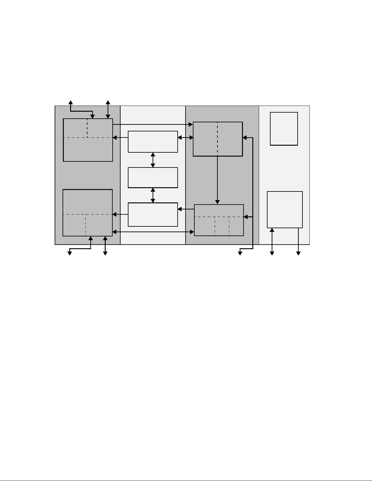
1.4 Processor Core Organization
The processor core consists of a 5-stage pipeline, separate instruction and data cache units, virtual
memory management unit (MMU), three timers, debug, and interfaces to other functions.
Figure 1-1 illustrates the logical organization of the PPC405.
PLB Master Instruction
Interface OCM
I-Cache I-Cache
ControllerArray
Instruction
Cache
Unit
Cache Units
Data
Cache
Unit
D-Cache D-Cache
ControllerArray
PLB Master Data
Interface OCM
MMU
Instruction Shadow
TLB
(4 Entry)
Unified TLB
(64 Entry)
Data Shadow
TLB
(8 Entry)
405 CPU
Fetch
Decode
Logic
Execute Unit (EXU)
32 x 32
GPR
3-Element
and
ALU
Figure 1-1. PPC405 Block Diagram
Fetch
Queue
(PFB1,
PFB0,
DCD)
MAC
APU/FPU
Timers
(FIT,
PIT,
Watchdog)
Timers
&
Debug
Debug Logic
(4 IAC,
2 DAC,
2 DVC)
JTAG Instruction
Trace
1.4.1 Instruction and Data Cache Controllers
The instruction cache unit (ICU) and data cache unit (DCU) enable concurrent accesses and
minimize pipeline stalls. The storage capacity of the cache units, which can range from 0KB–32KB,
depends upon the implementation. Both cache units are two-way set-associative, use a 32-byte line
size. The instruction set provides a rich assortment of cache control instructions, including
instructions to read tag information and data arrays. See Chapter 4, “Cache Operations,” for detailed
information about the ICU and DCU.
The cache units are PLB-compliant for use in the IBM Core+ASIC program.
1.4.1.1 Instruction Cache Unit
The ICU provides one or two instructions per cycle to the execution unit (EXU) over a 64-bit bus. A
line buffer (built into the output of the array for manufacturing test) enables the ICU to be accessed
only once for every four instructions, to reduce power consumption by the array.
The ICU can forward any or all of the words of a line fill to the EXU to minimize pipeline stalls caused
by cache misses. The ICU aborts speculative fetches abandoned by the EXU, eliminating
1-4 PPC405 Core User’s Manual
Page 29

unnecessary line fills and enabling the ICU to handle the next EXU fetch. Aborting abandoned
requests also eliminates unnecessary external bus activity to increase external bus utilization.
1.4.1.2 Data Cache Unit
The DCU transfers 1, 2, 3, 4, or 8 bytes per cycle, depending on the number of byte enables
presented by the CPU.The DCU contains a single-element command and store data queue to reduce
pipeline stalls; this queue enables the DCU to independently process load/store and cache control
instructions. Dynamic PLB request prioritization reduces pipeline stalls evenfurther.When the DCU is
busy with a low-priority request while a subsequent storage operation requested by the CPU is
stalled, the DCU automatically increases the priority of the current request to the PLB.
The DCU uses a two-line flush queue to minimize pipeline stalls caused by cache misses. Line
flushes are postponed until after a line fill is completed. Registers comprise the first position of the
flush queue; the line buffer built into the output of the array for manufacturing test serves as the
second position of the flush queue. Pipeline stalls are further reduced by forwarding the requested
word to the CPU during the line fill. Single-queued flushes are non-blocking. When a flush operation
is pending, the DCU can continue to access the array to determine subsequent load or store hits.
Under these conditions, load hits can occur concurrently with store hits to write-back memory without
stalling the pipeline. Requests abandoned by the CPU can also be aborted by the cache controller.
Additional DCU features enable the programmer to tailor performance for a given application. The
DCU can function in write-back or write-through mode, as controlled by the Data Cache Write-through
Register (DCWR) or the translation look-aside buffer (TLB). DCU performance can be tuned to
balance performance and memory coherency.Store-without-allocate, controlled by the SWOA field of
the Core Configuration Register 0 (CCR0), can inhibit line fills caused by store misses to further
reduce potential pipeline stalls and unwanted external bus traffic. Similarly, load-without-allocate,
controlled by CCR0[LWOA], can inhibit line fills caused by load misses.
1.4.2 Memory Management Unit
The 4GB address space of the PPC405 is presented as a flat address space.
The MMU provides address translation, protection functions, and storage attribute control for
embeddedembedded applications. The MMU supports demand paged virtual memory and other
management schemes that require precise control of logical to physical address mapping and flexible
memory protection. Working with appropriate system level software, the MMU provides the following
functions:
• Translation of the 4GB logical address space into physical addresses
• Independent enabling of instruction and data translation/protection
• Page level access control using the translation mechanism
• Software control of page replacement strategy
• Additional control over protection using zones
• Storage attributes for cache policy and speculative memory access control
The MMU can be disabled under software control. If the MMU is not used, the PPC405 core provides
other storage control mechanisms.
The translation lookaside buffer (TLB) is the hardware resource that controls translation and
protection. It consists of 64 entries, each specifying a page to be translated. The TLB is fully
Overview 1-5
Page 30

associative; a page entry can be placed anywhere in the TLB. The translation function of the MMU
occurs pre-cache for data accesses. Cache tags and indexing use physical addresses for data
accesses; instruction fetches are virtually indexed and physically tagged.
Software manages the establishment and replacement of TLB entries. This gives system software
significant flexibility in implementing a custom page replacement strategy. For example, to reduce
TLB thrashing or translation delays, software can reserve several TLB entries for globally accessible
static mappings. The instruction set provides several instructions to manage TLB entries. These
instructions are privileged and require the software to be executingin supervisor state. Additional TLB
instructions are provided to move TLB entry fields to and from GPRs.
The MMU divides logical storage into pages. Eight page sizes (1KB, 4KB, 16KB, 64KB, 256KB, 1MB,
4MB, 16MB) are simultaneously supported, so that, at any given time, the TLB can contain entries for
any combination of page sizes. For a logical to physical translation to occur, a valid entry for the page
containing the logical address must be in the TLB. Addresses for which no TLB entry exists cause
TLB-Miss exceptions.
To improve performance, 4 instruction-side and 8 data-side TLB entries are kept in shadow arrays.
The shadow arrays prevent TLB contention. Hardware manages the replacement and invalidation of
shadow-TLB entries; no system software action is required. The shadow arrays can be thought of as
level 1 TLBs, with the main TLB serving as a level 2 TLB.
When address translation is enabled, the translation mechanism provides a basic level of protection.
Physical addresses not mapped by a page entry are inaccessible when translation is enabled. Read
access is implied by the existence of the valid entry in the TLB. The EX and WR bits in the TLB entry
further define levels of access for the page, by permitting execute and write access, respectively.
The Zone Protection Register (ZPR) enables the system software to override the TLB access
controls. For example, the ZPR provides a way to deny read access to application programs. The
ZPR can be used to classify storage by type; access by type can be changed without manipulating
individual TLB entries.
The PowerPC Architecture provides WIU0GE (write-back/write through, cachability, user-defined 0,
guarded, endian) storage attributes that control memory accesses, using bits in the TLB or, when
address translation is disabled, storage attribute control registers.
When address translation is enabled (MSR[IR, DR] = 1), storage attribute control bits in the TLB
control the storage attributes associated with the current page. When address translation is disabled
(MSR[IR, DR] = 0), bits in each storage attribute control register control the storage attributes
associated with storage regions. Each storage attribute control register contains 32 fields. Each field
sets the associated storage attribute for a 128MB memory region. See “Real-Mode Storage Attribute
Control” on page 7-17 for more information about the storage attribute control registers.
1.4.3 Timer Facilities
The processor core contains a time base and three timers:
• Programmable Interval Timer (PIT)
• Fixed Interval Timer (FIT)
• Watchdog timer
1-6 PPC405 Core User’s Manual
Page 31

The time base is a 64-bit counter incremented either by an internal signal equal to the CPU clock rate
or by a separate external timer clock signal. No interrupts are generated when the time base rolls
over.
The PIT is a 32-bit register that is decremented at the same rate as the time base is incremented. The
user loads the PIT register with a value to create the desired delay. When a decrement occurs on a
PIT count of 1, the timer stops decrementing, a bit is set in the Timer Status Register (TSR), and a
PIT interrupt is generated. Optionally, the PIT can be programmed to reload automatically the last
value written to the PIT register, after which the PIT begins decrementing again.The Timer Control
Register (TCR) contains the interrupt enable for the PIT interrupt.
The FIT generates periodic interrupts based on selected bits in the time base. Users can select one of
four intervals for the timer period by setting the appropriate bits in the TCR. When the selected bit in
the time base changes from 0 to 1, a bit is set in the TSR and a FIT interrupt is generated. The FIT
interrupt enable is contained in the TCR.
The watchdog timer generates a periodic interrupt based on selected bits in the time base. Users can
select one of four time periods for the interval and the type of reset generated if the watchdog timer
expires twice without an intervening clear from software.
1.4.4 Debug
The processor core debug facilities include debug modes for the various types of debugging used
during hardware and software development. Also included are debug events that allow developers to
control the debug process. Debug modes and debug events are controlled using debug registers in
the chip. The debug registers are accessed either through software running on the processor, or
through the JTAG port. The JTAG port can also be used for board test.
The debug modes, events, controls, and interfaces provide a powerful combination of debug facilities
for hardware and software development tools.
1.4.4.1 Development Tool Support
The PPC405 supports a wide range of hardware and software development tools.
An operating system debugger is an example of an operating system-aware debugger, implemented
using software traps.
RISCWatch is an example of a development tool that uses the external debug mode, debug events,
and the JTAG port to support hardware and software development and debugging.
The RISCTrace™ feature of RISCWatch is an example of a development tool that uses the real-time
trace capability of the processor core.
1.4.4.2 Debug Modes
The internal, external,real-time-trace, and debug wait modes support a variety of debug tool used in
embedded systems development. These debug modes are described in detail in “Debug Modes” on
page 8-1.
1.4.5 Core Interfaces
The core provides a range of I/O interfaces that simplify the attachment of on-chip and off-chip
devices.
Overview 1-7
Page 32

1.4.5.1 Processor Local Bus
The PLB-compliant interface provides separate 32-bit address and 64-bit data buses for the
instruction and data sides.
1.4.5.2 Device Control Register Bus
The Device Control Register (DCR) bus supports the attachment of on-chip registers for device
control.
These registers are accessed using the mfdcr and mtdcr instructions.
1.4.5.3 Clock and Power Management
This interface supports several methods of clock distribution and power management.
1.4.5.4 JTAG
The JTAG port is enhanced to support the attachment of a debug tool such as the RISCWatch
product from IBM Microelectronics. Through the JTAG test access port, a debug tool can single-step
the processor and interrogate internal processor state to facilitate software debugging. The
enhancements comply with the IEEE 1149.1 specification for vendor-specific extensions, and are
therefore compatible with standard JTAG hardware for boundary-scan system testing.
1.4.5.5 Interrupts
The processor core provides an interface to an on-chip interrupt controller that is logically outside the
core. The interrupt controller combines asynchronous interrupt inputs from on-chip and off-chip
sources and presents them to the core using a pair of interrupt signals: critical and non-critical. The
sources of asynchronous interrupts are external signals, the JTAG/debug unit, and any implemented
peripherals.
1.4.5.6 Auxiliary Processor Unit
The auxiliary processor unit (APU) interface supports the attachment of auxiliary processor hardware
and the implementation of the associated instructions for improved performance in specialized
applications.
1.4.5.7 On-Chip Memory
The on-chip memory (OCM) interface supports the implementation of instruction- and data-side
memory that can be accessed at performance levels matching the cache arrays.
1.4.6 Data Types
Processor core operands are bytes, halfwords, and words. Multiple words or strings of bytes can be
transferredusing the load/store multiple and load/store string instructions. Data is represented in twos
complement notation or in unsigned fixed-point format.
The address of a multibyte operand is always the lowest memory address occupied by that operand.
Byte ordering can be selected as big endian (the lowest memory address of an operand contains its
most significant byte) or as little endian (the lowest memory address of an operand contains its least
1-8 PPC405 Core User’s Manual
Page 33

significant byte). See “Byte Ordering” on page 2-17 for more information about big and little endian
operation.
1.4.7 Processor Core Register Set Summary
The processor core registers can be grouped into basic categories based on function and access
mode: general purpose registers (GPRs), special purpose registers (SPRs), the machine state
register (MSR), the condition register (CR), and, in Core+ASIC implementations, device control
registers (DCRs).
Chapter 10, “Register Summary,” provides a register diagram and a register field description table for
each register.
1.4.7.1 General Purpose Registers
The processor core contains 32 GPRs; each register contains 32 bits. The contents of the GPRs can
be transferred from memory using load instructions and stored to memory using store instructions.
GPRs, which are specified as operands in many instructions, can also receive instruction results and
the contents of other registers.
1.4.7.2 Special Purpose Registers
Special Purpose Registers (SPRs), which are part of the PowerPC Architecture, are accessed using
the mtspr and mfspr instructions. SPRs control the use of the debug facilities, timers, interrupts,
storage control attributes, and other architected processor resources.
All SPRs are privileged (unavailable to user-mode programs), except the Count Register (CTR), the
Link Register (LR), SPR General Purpose Registers (SPRG4–SPRG7, read-only), and the Fixedpoint Exception Register (XER). Note that access to the Time Base Lower (TBL) and Time Base
Upper (TBU) registers, when addressed as SPRs, is write-only and privileged. However, when
addressed as Time Base Registers (TBRs), read access to these registers is not privileged. See
“Time Base Registers” on page 10-4 for more information.
1.4.7.3 Machine State Register
The PPC405 contains a 32-bit Machine State Register (MSR). The contents of a GPR can be written
to the MSR using the mtmsr instruction, and the MSR contents can be read into a GPR using the
mfmsr instruction. The MSR contains fields that control the operation of the processor core.
1.4.7.4 Condition Register
The PPC405 contains a 32-bit Condition Register (CR). These bits are grouped into eight 4-bit fields,
CR[CR0]–CR[CR7]. Instructions are provided to perform logical operations on CR fields and bits
within fields and to test CR bits within fields. The CR fields, which are set by compare instructions,
can be used to control branches. CR[CR0] can be set implicitly by arithmetic instructions.
1.4.7.5 Device Control Registers
DCRs, which are architecturally outside of the processor core, are accessed using the mtdcr and
mfdcr instructions. DCRs are used to control, configure, and hold status for various functional units
that are not part of the processor core. Although the PPC405 does not contain DCRs, the mtdcr and
mfdcr instructions are provided.
Overview 1-9
Page 34

The mtdcr and mfdcr instructions are privileged, for all DCRs. Therefore, all accesses to DCRs are
privileged. See “Privileged Mode Operation” on page 2-30.
All DCR numbers are reserved, and should be neither read nor written, unless they are part of an IBM
Core+ASIC implementation.
1.4.8 Addressing Modes
The processor core supports the following addressing modes, which enable efficient retrieval and
storage of data in memory:
• Base plus displacement addressing
• Indexed addressing
• Base plus displacement addressing and indexed addressing, with update
In the base plus displacement addressing mode, an effective address (EA) is formed by adding a
displacement to a base address contained in a GPR (or to an implied base of 0). The displacement is
an immediate field in an instruction.
In the indexed addressing mode, the EA is formed by adding an index contained in a GPR to a base
address contained in a GPR (or to an implied base of 0).
The base plus displacement and the indexed addressing modes also have a “with update” mode. In
“with update” mode, the effective address calculated for the current operation is saved in the base
GPR, and can be used as the base in the next operation. The “with update” mode relieves the
processor from repeatedly loading a GPR with an address for each piece of data, regardless of the
proximity of the data in memory.
1-10 PPC405 Core User’s Manual
Page 35

Chapter 2. Programming Model
The programming model of the PPC405 embedded processor core describes the following features
and operations:
• Memory organization and addressing, starting on page 2-1
• Registers, starting on page 2-2
• Data types and alignment, starting on page 2-16
• Byte ordering, starting on page 2-17
• Instruction processing, starting on page 2-23
• Branching control, starting on page 2-24
• Speculative accesses, starting on page 2-27
• Privileged mode operation, starting on page 2-30
• Synchronization, starting on page 2-33
• Instruction set, starting on page 2-36
2.1 User and Privileged Programming Models
The PPC405 executes programs in two modes, also referred to as states. Programs running in
privileged mode
instruction. These instructions and registers comprise the privileged programming model. In
, certain registers and instructions are unavailable to programs. This is also called the problem
mode
state. Those registers and instructions that are available comprise the user programming model.
Privileged mode provides operating system software access to all processor resources. Because
access to certain processor resources is denied in user mode, application software runs in user
mode. Operating system software and other application software is protected from the effects of an
errant application program.
Throughout this book, the terms user program and privileged programs are used to associate
programs with one of the programming models. Registers and instructions are described as user or
privileged. Privileged mode operation is described in detail in “Privileged Mode Operation” on
page 2-30.
(also referred to as the supervisor state) can access any register and execute any
user
2.2 Memory Organization and Addressing
The PowerPC Architecture defines a 32-bit, 4-gigabyte (GB) flat address space for instructions and
data
User’s manuals for standard products containing a PPC405 core describe the memory organizations
and physical address maps of the standard products.
Programming Model 2-1
Page 36

2.2.1 Storage Attributes
The PowerPC Architecture defines storage attributes that control data and instruction accesses.
Storage attributes are provided to control cache write-through policy (the W storage attribute),
cachability (the I storage attribute), memory coherency in multiprocessor environments (the M
storage attribute), and guarding against speculative memory accesses (the G storage attribute). The
IBM PowerPC Embedded Environment defines additional storage attributes for storage compression
(the U0 storage attribute) and byte ordering (the E storage attribute).
The PPC405 core provides two control mechanisms for the W, I, U0, G, and E attributes.Because the
PPC405 core does not provide hardware support for multiprocessor environments, the M storage
attribute, when present, has no effect.
When the PPC405 core operates in virtual mode (address translation is enabled), each storage
attribute is controlled by the W, I, U0, G, and E fields in the translation lookaside buffer (TLB) entry for
each memory page. The size of memory pages, and hence the size of storage attribute control
regions, is variable. Multiple sizes can be in effect simultaneously on different pages.
When the PPC405 core operates in real mode (address translation is disabled), storage attribute
control registers control the corresponding storage attributes. These registers are:
• Data Cache Write-through Register (DCWR)
• Data Cache Cachability Register (DCCR)
• Instruction Cache Cachability Register (ICCR)
• Storage Guarded Register (SGR)
• Storage Little-Endian Register (SLER)
• Storage User-defined 0 Register (SU0R)
Each storage attribute control register contains 32 bits; each bit controls one of thirty-two 128MB
storage attribute control regions. Bit 0 of each register controls the lowest-order region, with
ascending bits controlling ascending regions in memory. The storage attributes in each storage
attribute region are set independently of each other and of the storage attributes for other regions.
2.3 Registers
All PPC405 registers are listed in this section. Some of the frequently-used registers are described in
detail. Other registers are covered in their respective topic chapters (for example, the cache registers
are described in Chapter 4, “Cache Operations”). All registers are summarized in Chapter 10,
“Register Summary.”
The registers are grouped into categories: General Purpose Registers (GPRs), Special Purpose
Registers (SPRs), Time Base Registers (TBRs), the Machine State Register (MSR), the Condition
Register (CR), and, in standard products, Device Control Registers (DCRs). Different instructions are
used to access each category of registers.
For all registers with fields marked as
undefined
When reading from a register with a reserved field, ignore that field.
. That is, when writing to a register with a reserved field, write a 0 to the reserved field.
reserved
, the reserved fields should be written as 0 and read as
2-2 PPC405 Core User’s Manual
Page 37

Programming Note: A good coding practice is to perform the initial write to a register with
reserved fields as described, and to perform all subsequent writes to the register using a readmodify-write strategy: read the register, use logical instructions to alter defined fields, leaving
reserved fields unmodified, and write the register.
Figure 2-1 on page 2-4 illustrates the registers in the user and supervisor programming models.
Programming Model 2-3
Page 38

User Model
General-Purpose Registers
GPR0
GPR1
•
•
•
GPR31
SPR General Registers (read-only)
SPRG4
SPRG5
SPRG5
SPRG7
User SPR General Register 0 (read/write)
SPR 0x104
SPR 0x105
SPR 0x106
SPR 0x107
Supervisor Model
Machine State Register
MSR
Core Configuration Register
CCR0
SPR General Registers
SPRG0
SPRG1
SPRG2
SPRG3
SPRG4
SPRG5
SPRG6
SPR 0x3B3
SPR 0x110
SPR 0x111
SPR 0x112
SPR 0x113
SPR 0x114
SPR 0x115
SPR 0x116
Processor Version Register
PVR
Timer Facilities
Time Base Registers
TBL
TBU
Timer Control Register
TCR
Timer Status Register
TSR
Programmable Interval Timer
PIT
SPR 0x11F
SPR 0x11C
SPR 0x11D
SPR 0x3DA
SPR 0x3D8
SPR 0x3DB
USPRG0
Condition Register
CR
Fixed-Point Exception Register
XER
Link Register
LR
Count Register
CTR
Time Base Registers (read-only)
TBL
TBU
Storage Attribute Control Registers
DCCR
DCWR
ICCR
SGR
SLER
SU0R
SPR 0x100
SPR 0x001
SPR 0x008
SPR 0x009
TBR 0x10C
TBR 0x10D
SPR 0x3FA
SPR 0x3BA
SPR 0x3FB
SPR 0x3B9
SPR 0x3BB
SPR 0x3BC
Figure 2-1. PPC405 Programming Model—Registers
SPRG7
Exception Handling Registers
Exception Vector Prefix Register
EVPR
Exception Syndrome Register
ESR
Data Exception Address Register
DEAR SPR 0x3D5
Save/Restore Registers
SRR0
SRR1
SRR2
SRR3
Memory Management Registers
Process ID
PID
Zone Protection Register
ZPR
SPR 0x117
SPR 0x3D5
SPR 0x3D4
SPR 0x01A
SPR 0x01B
SPR 0x3DE
SPR 0x3DF
SPR 0x3B1
SPR 0x3B0
Debug Registers
Debug Status Register
DBSR
Debug Control Registers
DBCR0
DBCR1
Data Address Compares
DAC1
DAC2
Data Value Compares
DVC1
DVC2
Instruction Address Compares
IAC1
IAC2
IAC3
IAC4
Instruction Cache Debug Data Register
ICDBR SPR 0x3D3
SPR 0x3F0
SPR 0x3F2
SPR 0x3BD
SPR 0x3F6
SPR 0x3F7
SPR 0x3B6
SPR 0x3B7
SPR 0x3F4
SPR 0x3F5
SPR 0x3B4
SPR 0x3B5
2-4 PPC405 Core User’s Manual
Page 39

2.3.1 General Purpose Registers (R0-R31)
The PPC405 core contains thirty-two 32-bit general purpose registers (GPRs). Data from memory
can be read into GPRs using load instructions and the contents of GPRs can be written to memory
using store instructions. Most integer instructions use GPRs for source and destination operands.
See Table 10, “Register Summary,” on page 10-1 for the numbering of the GPRs.
0 31
Figure 2-2. General Purpose Registers (R0-R31)
0:31 General Purpose Register data
2.3.2 Special Purpose Registers
Special purpose registers (SPRs), which are part of the PowerPC Architecture and the IBM PowerPC
Embedded Environment, are accessed using the mtspr and mfspr instructions.
SPRs control the operation of debug facilities, timers, interrupts, storage control attributes, and other
architected processor resources. Table 10, “Register Summary,” on page 10-1 shows the mnemonic,
name, and number for each SPR. Table 2-1, “PPC405 SPRs,” on page 2-6 lists the PPC405 SPRs by
function and indicates the pages where the SPRs are described more fully.
Except for the Link Register (LR), the Count Register (CTR), the Fixed-point Exception Register
(XER), User SPR General 0 (USPRG0, and read access to SPR General 4–7 (SPRG4–SPRG7), all
SPRs are privileged. As SPRs, the registers TBL and TBU are privileged write-only; as TBRs, these
registers can be read in user mode. Unless used to access non-privileged SPRs, attempts to execute
mfspr and mtspr instructions while in user mode cause privileged violation program interrupts. See
“Privileged SPRs” on page 2-32.
Programming Model 2-5
Page 40

Table 2-1. PPC405 SPRs
Function Register Access Page
Configuration CCR0
Branch Control
Debug
Fixed-point Exception XER
General-Purpose SPR
Interrupts and Exceptions
Processor Version PVR
Privileged 4-11
CTR
LR
DAC1 DAC2
DBCR0 DBCR1
DBSR
DVC1 DVC2
IAC1 IAC2 IAC3 IAC4 Privileged 8-9
ICDBDR
SPRG0 SPRG1 SPRG2 SPRG3 Privileged 2-9
SPRG4 SPRG5 SPRG6 SPRG7 User read, privileged write 2-9
USPRG0
DEAR
ESR
EVPR
SRR0 SRR1
SRR2 SRR3
User 2-6
User 2-7
Privileged 8-9
Privileged 8-4
Privileged 8-7
Privileged 8-10
Privileged 4-14
User 2-7
User 2-9
Privileged 5-13
Privileged 5-11
Privileged 5-10
Privileged 5-9
Privileged 5-9
Privileged, read-only 2-10
Storage Attribute Control
Timer Facilities
Zone Protection ZPR
DCCR
DCWR
ICCR
SGR
SLER
SU0R
TBL TBU
PIT
TCR
TSR
Privileged 7-17
Privileged 7-17
Privileged 7-17
Privileged 7-17
Privileged 7-17
Privileged 7-17
Privileged, write-only 6-1
Privileged 6-4
Privileged 6-9
Privileged 6-8
Privileged 7-14
2.3.2.1 Count Register (CTR)
The CTR is written from a GPR using mtspr. The CTR contents can be used as a loop count that is
decremented and tested by some branch instructions. Alternatively, the CTR contents can specify a
target address for the bcctr instruction, enabling branching to any address.
The CTR is in the user programming model.
2-6 PPC405 Core User’s Manual
Page 41

0 31
Figure 2-3. Count Register (CTR)
0:31 Count Used as count for branch conditional with
decrement instructions, or as address for
branch-to-counter instructions.
2.3.2.2 Link Register (LR)
The LR is written from a GPR using mtspr, and by branch instructions that have the LK bit set to 1.
Such branch instructions load the LR with the address of the instruction following the branch
instruction. Thus, the LR contents can be used as the return address for a subroutine that was called
using the branch.
The LR contents can be used as a target address for the bclr instruction. This allows branching to any
address.
When the LR contents represent an instruction address, LR
are assumed to be 0, because all
30:31
instructions must be word-aligned. However, when LR is read using mfspr, all 32 bits are returned as
written.
The LR is in the user programming model.
0 31
Figure 2-4. Link Register (LR)
0:31 Link Register contents If (LR) represents an instruction address,
LR
should be 0.
30:31
2.3.2.3 Fixed Point Exception Register (XER)
The XER records overflow and carry conditions generated by integer arithmetic instructions.
The Summary Overflow(SO) field is set to 1 when instructions cause the Overflow (OV) field to be set
to 1. The SO field does not necessarily indicate that an overflow occurred on the most recent
arithmetic operation, but that an overflow occurred since the last clearing of XER[SO]. mtspr(XER)
sets XER[SO, OV] to the value of bit positions 0 and 1 in the source register, respectively.
Programming Model 2-7
Page 42

Once set, XER[SO] is not reset until an mtspr(XER) is executed with data that explicitly puts a 0 in
the SO bit, or until an mcrxr instruction is executed.
XER[OV] is set to indicate whether an instruction that updates XER[OV] produces a result that
“overflows” the 32-bit target register. XER[OV] = 1 indicates overflow. For arithmetic operations, this
occurs when an operation has a carry-in to the most-significant bit of the result that does not equal
the carry-out of the most-significant bit (that is, the exclusive-or of the carry-in and the carry-out is 1).
The following instructions set XER[OV] differently. The specific behavior is indicated in the instruction
descriptions in Chapter 9, “Instruction Set.”
• Move instructions:
mcrxr, mtspr(XER)
• Multiply and divide instructions:
mullwo, mullwo., divwo, divwo., divwuo, divwuo
The Carry (CA) field is set to indicate whether an instruction that updates XER[CA] produces a result
that has a carry-out of the most-significant bit. XER[CA] = 1 indicates a carry.
The following instructions set XER[CA] differently.The specific behavior is indicated in the instruction
descriptions in Chapter 9, “Instruction Set.”
• Move instructions
mcrxr, mtspr(XER)
• Shift-algebraic operations
sraw, srawi
The Transfer Byte Count (TBC) field is the byte count for load/store string instructions.
The XER is part of the user programming model.
CA
SO
0123 24 25 31
OV
TBC
Figure 2-5. Fixed Point Exception Register (XER)
0 SO Summary Overflow
0 No overflow has occurred.
1 Overflow has occurred.
1 OV Overflow
0 No overflow has occurred.
0 Overflow has occurred.
2 CA Carry
0 Carry has not occurred.
1 Carry has occurred.
Can be
instructions; can be
mcrxr.
Can be
instructions; can be
mcrxr, or “o” form instructions.
Can be
instructions that update the CA field; can
be
arithmetic instructions that update the CA
field.
set
by mtspr or by using “o” form
reset
set
by mtspr or by using “o” form
reset
set
by mtspr or arithmetic
reset
by mtspr, by mcrxr, or by
by mtspr or by
by mtspr, by
2-8 PPC405 Core User’s Manual
Page 43

3:24 Reserved
25:31 TBC Transfer Byte Count Used by lswx and stswx; written by mtspr.
Table 2-2 and Table 2-3 list the PPC405 instructions that update the XER. In the tables, the syntax
“[o]” indicates that the instruction has an “o” form that updates XER[SO,OV], and a “non-o” form. The
syntax “[.]” indicates that the instruction has a “record” form that updates CR[CR0] (see “Condition
Register (CR)” on page 2-10), and a “non-record” form.
Table 2-2. XER[CA] Updating Instructions
Integer Arithmetic
Add Subtract
Integer
Shift
Shift
Right
Algebraic
Processor
Control
Register
Management
addc[o][.]
adde[o][.]
addic[.]
addme[o][.]
addze[o][.]
subfc[o][.]
subfe[o][.]
subfic
subfme[o][.]
subfze[o][.]
Table 2-3. XER[SO,OV] Updating Instructions
Integer Arithmetic Auxiliary Processor
Add Subtract Multiply Divide Negate
addo[.]
addco[.]
addeo[.]
addmeo[.]
addzeo[.]
subfo[.]
subfco[.]
subfeo[.]
subfmeo[.]
subfzeo[.]
mullwo[.] divwo[.]
divwuo[.]
nego[.] macchwo[.]
sraw[.]
srawi[.]
Accumulate
macchwso[.]
macchwsuo[.]
macchwuo[.]
machhwo[.]
machhwso[.]
machhwsuo[.]
machhwuo[.]
maclhwo[.]
maclhwso[.]
maclhwsuo[.]
maclhwuo[.]
mtspr
mcrxr
Multiply-
Negative
Multiply-
Accumulate
nmacchwo[.]
nmacchwso[.]
nmachhwo[.]
nmachhwso[.]
nmaclhwo[.]
nmaclhwso[.]
Processor
Control
Register
Management
mtspr
mcrxr
2.3.2.4 Special Purpose Register General (SPRG0–SPRG7)
USPRG0 and SPRG0–SPRG7 are provided for general purpose software use. For example, these
registers are used as temporary storage locations. For example, an interrupt handler might save the
contents of a GPR to an SPRG, and later restore the GPR from it. This is faster than a save/restore to
a memory location. These registers are written using mtspr and read using mfspr.
Access to USPRG0 is non-privileged for both read and write.
Programming Model 2-9
Page 44

SPRG0–SPRG7 provide temporary storage locations. For example, an interrupt handler might save
the contents of a GPR to an SPRG, and later restore the GPR from it. This is faster than performing a
save/restore to memory. These registers are written by mtspr and read by mfspr.
Access to SPRG0–SPRG7 is privileged, except for read access to SPRG4–SPRG7. See “Privileged
SPRs” on page 2-32 for more information.
0 31
Figure 2-6. Special Purpose Register General (SPRG0–SPRG7)
0:31 General data Software value; no hardware usage.
2.3.2.5 Processor Version Register (PVR)
The PVR is a read-only register that uniquely identifies a standard product or Core+ASIC
implementation. Software can examinethe PVR to recognize implementation-dependent featuresand
determine available hardware resources.
Access to the PVR is privileged. See “Privileged SPRs” on page 2-32 for more information.
OWN
0 1112 1516 2122 2526 31
UDEF
CAS
PCL
AID
Figure 2-7. Processor Version Register (PVR)
0:11 OWN Owner Identifier Identifies the owner of a core
12:15 PCF Processor Core Family Identifies the processor core family.
16:21 CAS Cache Array Sizes Identifies the cache array sizes.
22:25 PCL Processor Core Version Identifies the core version for a specific
combination of PVR[PCF] and PVR[CAS]
26:31 AID ASIC Identifier Assigned sequentially; identifies an ASIC
function, version, and technology
2.3.3 Condition Register (CR)
The CR contains eight 4-bit fields (CR0–CR7), as shown in Figure 3-8. The fields contain conditions
detected during the executionof integer or logical compare instructions, as indicated in the instruction
2-10 PPC405 Core User’s Manual
Page 45

descriptions in Chapter 9, “Instruction Set.” The CR contents can be used in conditional branch
instructions.
The CR can be modified in any of the following ways:
• mtcrf sets specified CR fields by writing to the CR from a GPR, under control of a mask specified
as an instruction field.
• mcrf sets a specified CR field by copying another CR field to it.
• mcrxr copies certain bits of the XER into a designated CR field, and then clears the corresponding
XER bits.
• The “with update” forms of integer instructions implicitly update CR[CR0].
• Integer compare instructions update a specified CR field.
• Auxiliary processor instructions can update a specified CR field (including the implicit update of
CR[CR1] by certain floating-point operations).
• The CR-logical instructions update a specified CR bit with the result of a logical operation on a
specified pair of CR bit fields.
• Conditional branch instructions can test a CR bit as one of the branch conditions.
If a CR field is set by a compare instruction, the bits are set as described in “CR Fields after Compare
Instructions.”
The CR is part of the user programming model.
CR0
0 3 4 7 8 1112 1516 1920 2324 2728 31
CR1
CR2
CR3
CR4
CR5
CR6
CR7
Figure 2-8. Condition Register (CR)
0:3 CR0 Condition Register Field 0
4:7 CR1 Condition Register Field 1
8:11 CR2 Condition Register Field 2
12:15 CR3 Condition Register Field 3
16:19 CR4 Condition Register Field 4
20:23 CR5 Condition Register Field 5
24:27 CR6 Condition Register Field 6
28:31 CR7 Condition Register Field 7
2.3.3.1 CR Fields after Compare Instructions
Compare instructions compare the values of two registers. The two types of compare instructions,
arithmetic
and
logical
, are distinguished by the interpretation given to the 32-bit values. For
Programming Model 2-11
arithmetic
Page 46

compares, the values are considered to be signed, where 31 bits represent the magnitude and the
logical
most-significant bit is a sign bit. For
compares, the values are considered to be unsigned, so
all 32 bits represent magnitude. There is no sign bit. As an example, consider the comparison of 0
with 0xFFFFFFFF. In an
logical
compare, 0xFFFFFFFF is larger.
arithmetic
compare, 0 is larger, because 0xFFFF FFFF represents –1; in a
A compare instruction can direct its CR update to any CR field. The first data operand of a compare
instruction specifies a GPR. The second data operand specifies another GPR, or immediate data
derived from the IM field of the immediate instruction form. The contents of the GPR specified by the
first data operand are compared with the contents of the GPR specified by the second data operand
(or with the immediate data). See descriptions of the compare instructions (page 9-34 through
page 9-37) for precise details.
After a compare, the specified CR field is interpreted as follows:
LT (bit 0) The first operand is less than the second operand.
GT (bit 1) The first operand is greater than the second operand.
EQ (bit 2) The first operand is equal to the second operand.
SO (bit 3) Summary overflow; a copy of XER[SO].
2.3.3.2 The CR0 Field
After the execution of compare instructions that update CR[CR0], CR[CR0] is interpreted as
described in “CR Fields after Compare Instructions” on page 2-11. The “dot” forms of arithmetic and
logical instructions also alter CR[CR0]. After most instructions that update CR[CR0], the bits of CR0
are interpreted as follows:
LT (bit 0) Less than 0; set if the most-significant bit of the 32-bit result is 1.
GT (bit 1)
Greater than 0; set if the 32-bit result is non-zero and the most-
significant bit of the result is 0.
EQ (bit 2) Equal to 0; set if the 32-bit result is 0.
SO (bit 3) Summary overflow; a copy of XER[SO] at instruction completion.
The CR[CR0]
LT, GT, EQ
subfields are set as the result of an algebraic comparison of the instruction
result to 0, regardless of the type of instruction that sets CR[CR0]. If the instruction result is 0, the EQ
subfield is set to 1. If the result is not 0, either LT or GT is set, depending on the value of the mostsignificant bit of the result.
When updating CR[CR0], the most significant bit of an instruction result is considered a sign bit, even
for instructions that produce results that are not usually thought of as signed. For example, logical
instructions such as and., or.,and nor.update CR[CR0]
LT, GT, EQ
using such an arithmetic comparison
to 0, although the result of such a logical operation is not actually an arithmetic result.
If an arithmetic overflow occurs, the “sign” of an instruction result indicated in CR[CR0]
LT, GT, EQ
might
not represent the “true” (infinitely precise) algebraic result of the instruction that set CR0. For
example, if an add. instruction adds two large positive numbers and the magnitude of the result
cannot be represented as a twos-complement number in a 32-bit register, an overflow occurs and
CR[CR0]
are set, although the infinitely precise result of the add is positive.
LT, SO
2-12 PPC405 Core User’s Manual
Page 47

Adding the largest 32-bit twos-complement negative number, 0x8000 0000, to itself results in an
arithmetic overflow and 0x0000 0000 is recorded in the target register. CR[CR0]
EQ, SO
is set,
indicating a result of 0, but the infinitely precise result is negative.
The CR[CR0]
cause an overflow, but even for these instructions CR[CR0]
subfield is a copy of XER[SO]. Instructions that do not alter the XER[SO] bit cannot
SO
is a copy of XER[SO].
SO
Some instructions set CR[CR0] differently or do not specifically set any of the subfields. These
instructions include:
• Compare instructions
cmp, cmpi, cmpl, cmpli
• CR logical instructions
crand, crandc, creqv, crnand, crnor, cror, crorc, crxor, mcrf
• Move CR instructions
mtcrf, mcrxr
• stwcx.
The instruction descriptions provide detailed information about how the listed instructions alter
CR[CR0].
2.3.4 The Time Base
The PowerPC Architecture provides a 64-bit time base. “Time Base” on page 6-1 describes the
architected time base. Access to the time base is through two 32-bit time base registers (TBRs). The
least-significant 32 bits of the time base are read from the Time Base Lower (TBL) register and the
most-significant 32 bits are read from the Time Base Upper (TBU) register.
User-mode access to the time base is read-only, and there is no explicitly privileged read access to
the time base.
The mftb instruction reads from TBL and TBU. Writing the time base is accomplished by moving the
contents of a GPR to a pair of SPRs, which are also called TBL and TBU, using mtspr.
Table 2-4 shows the mnemonics and names of the TBRs.
Table 2-4. Time Base Registers
Mnemonic Register Name Access
TBL Time Base Lower (Read-only) Read-only
TBU Time Base Upper (Read-only) Read-only
2.3.5 Machine State Register (MSR)
The Machine State Register (MSR) controls processor core functions, such as the enabling or
disabling of interrupts and address translation.
The MSR is written from a GPR using the mtmsr instruction. The contents of the MSR can be read
into a GPR using the mfmsr instruction. MSR[EE] is set or cleared using the wrtee or wrteei
instructions.
Programming Model 2-13
Page 48

The MSR contents are automatically saved, altered, and restored by the interrupt-handling
mechanism. See “Machine State Register (MSR)” on page 5-7.
APE
CE
PR
DWE
FE1
DRME
0 567 11 12 13 14 15 16 17 18 19 20 21 22 23 24 25 26 27 28 31
AP
WE
EE
FP
FE0
DE
IR
Figure 2-9. Machine State Register (MSR)
0:5 Reserved
6 AP Auxiliary Processor Available
0 APU not available.
1 APU available.
7:11
12 APE APU Exception Enable
13 WE Wait State Enable
14 CE Critical Interrupt Enable
Reserved
0 APU exception disabled.
1 APU exception enabled.
0 The processor is not in the wait state.
1 The processor is in the wait state.
0 Critical interrupts are disabled.
1 Critical interrupts are enabled.
If MSR[WE] = 1, the processor remains in
the wait state until an interrupt is taken, a
reset occurs, or an external debug tool
clears WE.
Controls the critical interrupt input and
watchdog timer first time-out interrupts.
15
Reserved
16 EE External Interrupt Enable
0 Asynchronous interruptsare disabled.
1 Asynchronous interrupts are enabled.
17 PR Problem State
0 Supervisor state (all instructions
allowed).
1 Problem state (some instructions not
allowed).
18 FP Floating Point Available
0 The processor cannot execute floating-
point instructions
1 The processor can execute floating-point
instructions
19 ME Machine Check Enable
0 Machine check interrupts are disabled.
1 Machine check interrupts are enabled.
Controls the non-critical external interrupt
input, PIT, and FIT interrupts.
2-14 PPC405 Core User’s Manual
Page 49

20 FE0 Floating-point exception mode 0
0 If MSR[FE1] = 0, ignore exceptions
mode; if MSR[FE1] = 1, imprecise
nonrecoverable mode
1 If MSR[FE1] = 0, imprecise recoverable
mode; if MSR[FE1] = 1, precise mode
21 DWE Debug Wait Enable
0 Debug wait mode is disabled.
1 Debug wait mode is enabled.
22 DE Debug Interrupts Enable
0 Debug interrupts are disabled.
1 Debug interrupts are enabled.
23 FE1 Floating-point exception mode 1
0 If MSR[FE0] = 0, ignore exceptions
mode; if MSR[FE0] = 1, imprecise
recoverable mode
1 If MSR[FE0] = 0, imprecise non-
recoverable mode; if MSR[FE0]= 1,
precise mode
24:25
26 IR Instruction Relocate
27 DR Data Relocate
28:31
Reserved
0 Instruction address translation is
disabled.
1 Instruction address translation is
enabled.
0 Data address translation is disabled.
1 Data address translation is enabled.
Reserved
2.3.6 Device Control Registers
Device Control Registers (DCRs), on-chip registers that exist architecturally outside the processor
core, are not part of the IBM PowerPC Embedded Environment. The Embedded Environment simply
defines the existence of a DCR address space and the instructions that access the DCRs, but does
not define any DCRs. The instructions that access the DCRs are mtdcr (move to device control
register) and mfdcr (move from device control register).
DCRs are used to control the operations of on-chip buses, peripherals, and some processor behavior.
Programming Model 2-15
Page 50

2.4 Data Types and Alignment
The data types consist of bytes (eight bits), halfwords (two bytes), words (four bytes), and strings (1 to
128 bytes). Figure 2-10 shows the byte, halfword, and word data types and their bit and byte
definitions for big endian representations of values. Note that PowerPC bit numbering is reversed
from industry conventions; bit 0 represents the most significant bit of a value.
Byte
Bit
0
0
0
0
0
0
1
1
15
Byte
7
2
Halfword
3
Word
31
Figure 2-10. PPC405 Data Types
Data is represented in either twos-complement notation or in an unsigned integer format; data
representation is independent of alignment issues.
The address of a data object is always the lowest address of any byte comprising the object.
All instructions are words, and are word-aligned (the lowest byte address is divisible by 4).
2.4.1 Alignment for Storage Reference and Cache Control Instructions
The storage reference instructions (loads and stores; see Table 2-12, “Storage Reference
Instructions,” on page 2-37) move data to and from storage. The data cache control instructions listed
in Table 2-21, “Cache Management Instructions,” on page 2-41, control the contents and operation of
the data cache unit (DCU). Both types of instructions form an effective address (EA). The method of
calculating the EA for the storage reference and cache control instructions is detailed in the
description of those instructions. See Chapter 9, “Instruction Set,” for more information.
Cache control instructions ignore the five least significant bits of the EA; no alignment restrictions
exist in the DCU because of EAs. However, storage control attributes can cause alignment
exceptions. When data address translation is disabled and a dcbz instruction references a storage
region that is non-cachable, or for which write-through caching is the write strategy, an alignment
exception is taken. Such exceptions result from the storage control attributes, not from EA alignment.
The alignment exception enables system software to emulate the write-through function.
Alignment requirements for the storage reference instructions and the dcread instruction depend on
the particular instruction. Table 2-5, “Alignment Exception Summary,” on page 2-17, summarizes the
instructions that cause alignment exceptions.
The data targets of instructions are of types that depend upon the instruction. The load/store
instructions have the following “natural” alignments:
• Load/store word instructions have word targets, word-aligned.
• Load/ store halfword instructions have halfword targets, halfword-aligned.
• Load/store byte instructions have byte targets, byte-aligned (that is, any alignment).
2-16 PPC405 Core User’s Manual
Page 51

Misalignments are addresses that are not naturally aligned on data type boundaries. An address not
divisible by four is misaligned with respect to word instructions. An address not divisible by two is
misaligned with respect to halfword instructions. The PPC405 core implementation handles
misalignments within and across word boundaries, but there is a performance penalty because
additional cycles are required.
2.4.2 Alignment and Endian Operation
The endian storage control attribute does not affect alignment behavior. In little endian storage
regions, the alignment of data is treated as it is in big endian storage regions; no special alignment
exceptions occur when accessing data in little endian storage regions. Note that the alignment
exceptions that apply to big endian region accesses also apply to little endian storage region
accesses.
2.4.3 Summary of Instructions Causing Alignment Exceptions
Table 2-5 summarizes the instructions that cause alignment exceptions and the conditions under
which the alignment exceptions occur.
Table 2-5. Alignment Exception Summary
Instructions Causing Alignment
Exceptions Conditions
dcbz EA in non-cachable or write-through storage
dcread, lwarx, stwcx. EA not word-aligned
APU load/store halfword EA not halfword-aligned
APU load/store word EA not word-aligned
APU load/store doubleword EA not word-aligned
2.5 Byte Ordering
The following discussion describes the “endianness” of the PPC405, which, by default and in normal
use is “big endian.”
If scalars (individual data items and instructions) were indivisible, “byte ordering” would not be a
concern. It is meaningless to consider the order of bits or groups of bits within a byte, the smallest
addressable unit of storage; nothing can be observed about such order.Only when scalars, which the
programmer and processor regard as indivisible quantities, can comprise more than one addressable
unit of storage does the question of byte order arise.
For a machine in which the smallest addressable unit of storage is the 32-bit word, there is no
question of the ordering of bytes within words. All transfers of individual scalars between registers and
storage are of words, and the address of the byte containing the high-order eight bits of a scalar is the
same as the address of any other byte of the scalar.
For the PowerPC Architecture, as for most computer architectures currently implemented, the
smallest addressable unit of storage is the 8-bit byte. Other scalars are halfwords, words, or
doublewords, which consist of groups of bytes. When a word-length scalar is moved from a register to
Programming Model 2-17
Page 52

storage, the scalar is stored in four consecutive byte addresses. It thus becomes meaningful to
discuss the order of the byte addresses with respect to the value of the scalar: that is, which byte
contains the highest-order eight bits of the scalar, which byte contains the next-highest-order eight
bits, and so on.
Given a scalar that contains multiple bytes, the choice of byte ordering is essentially arbitrary. There
are 4! = 24 ways to specify the ordering of four bytes within a word, but only two of these orderings
are commonly used:
• The ordering that assigns the lowest address to the highest-order (“leftmost”) eight bits of the
scalar, the next sequential address to the next-highest-order eight bits, and so on.
This ordering is called
number, comes first in storage.
• The ordering that assigns the lowest address to the lowest-order (“rightmost”) eight bits of the
scalar, the next sequential address to the next-lowest-order eight bits, and so on.
This ordering is called
number, comes first in storage.
big endian
little endian
because the “big end” of the scalar, considered as a binary
because the “little end” of the scalar, considered as a binary
2.5.1 Structure Mapping Examples
The following C language structure,s, contains an assortment of scalars and a character string. The
comments show the value assumed to be in each structure element; these values show how the
bytes comprising each structure element are mapped into storage.
struct {
int a; /* 0x1112_1314 word */
long long b; /* 0x2122_2324_2526_2728 doubleword */
char *c; /* 0x3132_3334 word */
char d[7]; /* 'A','B','C','D','E','F','G' array of bytes */
short e; /* 0x5152 halfword */
int f; /* 0x6162_6364 word */
} s;
C structure mapping rules permit the use of padding (skipped bytes) to align scalars on desirable
boundaries. The structure mapping examples show each scalar aligned at its natural boundary. This
a
alignment introduces padding of four bytes between
e
bytes between
mappings.
2-18 PPC405 Core User’s Manual
andf. The same amount of padding is present in both big endian and little endian
andb, one byte betweend ande, and two
Page 53

2.5.1.1 Big Endian Mapping
The big endian mapping of structures follows. (The data is highlighted in the structure mappings.
Addresses, in hexadecimal, are below the data stored at the address. The contents of each byte, as
s
defined in structure
, is shown as a (hexadecimal) number or character (for the string elements).
11 12 13 14
0x00 0x01 0x02 0x03 0x04 0x05 0x06 0x07
21 22 23 24 25 26 27 28
0x08 0x09 0x0A 0x0B 0x0C 0x0D 0x0E 0x0F
31 32 33 34 'A' 'B' 'C' 'D'
0x10 0x11 0x12 0x13 0x14 0x15 0x16 0x17
'E' 'F' 'G' 51 52
0x18 0x19 0x1A 0x1B 0x1C 0x1D 0x1E 0x1F
61 62 63 64
0x20 0x21 0x22 0x23 0x24 0x25 0x26 0x27
2.5.1.2 Little Endian Mapping
Structures is shown mapped little endian.
14 13 12 11
0x00 0x01 0x02 0x03 0x04 0x05 0x06 0x07
28 27 26 25 24 23 22 21
0x08 0x09 0x0A 0x0B 0x0C 0x0D 0x0E 0x0F
34 33 32 31 'A' 'B' 'C' 'D'
0x10 0x11 0x12 0x13 0x14 0x15 0x16 0x17
'E' 'F' 'G' 52 51
0x18 0x19 0x1A 0x1B 0x1C 0x1D 0x1E 0x1F
64 63 62 61
0x20 0x21 0x22 0x23 0x24 0x25 0x26 0x27
2.5.2 Support for Little Endian Byte Ordering
This book describes the processor as if it operated only in a big endian fashion. In fact, the IBM
PowerPC Embedded Environment also supports little endian operation.
The PowerPC little endian mode, defined in the PowerPC Architecture, is not implemented.
2.5.3 Endian (E) Storage Attribute
The endian (E) storage attribute supports direct connection of the PPC405 core to little endian
peripherals and to memory containing little endian instructions and data. For every storage reference
(instruction fetch or load/store access), an E storage attribute is associated with the storage region of
the reference. The E attribute specifies whether that region is organized as big endian (E = 0) or little
endian (E = 1).
Programming Model 2-19
Page 54

When address translation is enabled (MSR[IR] = 1 or MSR[DR] = 1), the E field in the corresponding
TLB entry controls the endianness of a memory region. When address translation is disabled
(MSR[IR] = 0 or MSR[DR] = 0), the SLER controls the endianness of a memory region.
Bytes in storage that are accessed as little endian are arranged in true little endian format. The
PPC405 does not support the little endian mode defined in the PowerPC architecture and used in
PPC401xx and PPC403xx processors. Furthermore, no address modification is performed when
accessing storage regions programmed as little endian. Instead, the PPC405 reorders the bytes as
they are transferred between the processor and memory.
The on-the-fly reversal of bytes in little endian storage regions is handled in one of two ways,
depending on whether the storage access is an instruction fetch or a data access (load/store). The
following sections describe byte reordering for the two kinds of storage accesses.
2.5.3.1 Fetching Instructions from Little Endian Storage Regions
Instructions are words (four bytes) that are aligned on word boundaries in memory. As such,
instructions in a big endian memory region are arranged with the most significant byte (MSB) of the
instruction word at the lowest address.
p
Consider the big endian mapping of instruction
p
= add r7, r7, r4:
MSB LSB
0x00 0x01 0x02 0x03
at address 00, where, for example,
p
On the other hand, in the little endian mapping instruction
is arranged with the least significant byte
(LSB) of the instruction word at the lowest numbered address:
LSB MSB
0x00 0x01 0x02 0x03
When an instruction is fetched from memory, the instruction must be placed in the instruction queue in
the proper order. The execution unit assumes that the MSB of an instruction word is at the lowest
address. Therefore, when instructions are fetched from little endian storage regions, the four bytes of
an instruction word are reversed before the instruction is decoded. In the PPC405 core, the byte
reversal occurs between memory and the instruction cache unit (ICU). The ICU always stores
instructions in big endian format, regardless of whether the memory region containing the instruction
is programmed as big endian or little endian. Thus, the bytes are already in the proper order when an
instruction is transferred from the ICU to the decode stage of the pipeline.
If a storage region is reprogrammed from one endian format to the other, the storage region must be
reloaded with program and data structures in the appropriate endian format. If the endian format of
instruction memory changes, the ICU must be made coherent with the updates. The ICU must be
invalidated and the updated instruction memory using the new endian format must be fetched so that
the proper byte ordering occurs before the new instructions are placed in the ICU.
2-20 PPC405 Core User’s Manual
Page 55

2.5.3.2 Accessing Data in Little Endian Storage Regions
Unlike instruction fetches from little endian storage regions, data accesses from little endian storage
not
regions are
depends on the data type (byte, halfword, or word) of a specific data item. It is only when moving a
data item
required. Therefore, byte reversal during load/store accesses is performed between the DCU and the
GPR.
When accessing data in a little endian storage region:
• For byte loads/stores, no reordering occurs.
• For halfword loads/stores, bytes are reversed within the halfword.
• For word loads/stores, bytes are reversed within the word.
Note that this applies, regardless of data alignment.
The big endian and little endian mappings of the structure
on page 2-18, demonstrate how the size of an item determines its byte ordering. For example:
• The word
byte-reversed between memory and the DCU. Data byte ordering, in memory,
of a specific type
a
has its four bytes reversed within the word spanning addresses 0x00–0x03.
from or to a GPR that it becomes known what type of byte reversal is
s
, shown in “Structure Mapping Examples”
• The halfword
Note that the array of bytes
little endian mappings are compared. For example, the character 'A' is located at address 0x14 in
both the big endian and little endian mappings.
In little endian storage regions, the alignment of data is treated as it is in big endian storage regions.
Unlike PowerPC little endian mode, no special alignment exceptions occur when accessing data in
little endian storage regions.
e
has its two bytes reversed within the halfword spanning addresses 0x1C–0x1D.
d
, where each data item is a byte, is not reversed when the big endian and
2.5.3.3 PowerPC Byte-Reverse Instructions
For big endian storage regions, normal load/store instructions move the more significant bytes of a
register to and from the lower-numbered memory addresses. The load/store with byte-reverse
instructions move the more significant bytes of the register to and from the higher numbered memory
addresses.
As Figure 2-11 through Figure 2-14 illustrate, a normal store to a big endian storage region is the
same as a byte-reverse store to a little endian storage region. Conversely, a normal store to a little
endian storage region is the same as a byte-reverse store to a big endian storage region.
Programming Model 2-21
Page 56

Figure 2-11 illustrates the contents of a GPR and memory (starting at address 00) after a normal
load/store in a big endian storage region.
MSB
11 12 13 14
11 12 13 14
0x00 0x01 0x02 0x03
LSB
GPR
Memory
Figure 2-11. Normal Word Load or Store (Big Endian Storage Region)
Note that the results are identical to the results of a load/store with byte-reverse in a little endian
storage region, as illustrated in Figure 2-12.
MSB
11 12 13 14
11 12 13 14
0x00 0x01 0x02 0x03
LSB
GPR
Memory
Figure 2-12. Byte-Reverse Word Load or Store (Little Endian Storage Region)
Figure 2-13 illustrates the contents of a GPR and memory (starting at address 00) after a load/store
with byte-reverse in a big endian storage region.
MSB
11 12 13 14
14 13 12 11
0x00 0x01 0x02 0x03
LSB
GPR
Memory
Figure 2-13. Byte-Reverse Word Load or Store (Big Endian Storage Region)
2-22 PPC405 Core User’s Manual
Page 57

Note that the results are identical to the results of a normal load/store in a little endian storage region,
as illustrated in Figure 2-14.
MSB
11 12 13 14
14 13 12 11
0x00 0x01 0x02 0x03
LSB
GPR
Memory
Figure 2-14. Normal Word Load or Store (Little Endian Storage Region)
The E storage attribute augments the byte-reverse load/store instructions in two important ways:
• The load/store with byte-reverse instructions do not solve the problem of fetching instructions from
a storage region in little endian format.
Only the endian storage attribute mechanism supports the fetching of little endian program images.
• Typical compilers cannot make general use of the byte-reverse load/store instructions, so these
instructions are ordinarily used only in device drivers written in hand-coded assembler.
Compilers can, however, take full advantage of the endian storage attribute mechanism, enabling
application programmers working in a high-level language, such as C, to compile programs and
data structures into little endian format.
2.6 Instruction Processing
The instruction pipeline, illustrated in Figure 2-15, contains three queue locations: prefetch buffer 1
(PFB1), prefetch buffer 0 (PFB0), and decode (DCD). This queue implements a pipeline with the
following functional stages: fetch, decode, execute, write-back and load write-back. Instructions are
fetched from the instruction cache unit (ICU), placed in the instruction queue, and eventually
dispatched to the execution unit (EXU).
Instructions are fetched from the ICU at the request of the EXU. Cachable instructions are forwarded
directly to the instruction queue and stored in the ICU cache array. Non-cachable instructions are also
forwarded directly to the instruction queue, but are not stored in the ICU cache array. Fetched
instructions drop to the empty queue location closest to the EXU. When there is room in the queue,
instructions can be returned from the ICU two at a time. If the queue is empty and the ICU is returning
two instructions, one instruction drops into DCD while the other drops into PFB0. PFB1 buffers
instructions when the pipeline stalls.
Programming Model 2-23
Page 58

Branch instructions are examined in DCD and PFB0 while all other instructions are decoded in DCD.
All instructions must pass through DCD before entering the EXU. The EXU contains the execute,
write-back and load write-back stages of the pipe. The results of most instructions are calculated
during the execute stage and written to the GPR file during the write back stage. Load instructions
write the GPR file during the load write-back stage.
ICU
Fetch
PFB1
Instruction
Queue
PFB0
DCD
Dispatch
EXU
Figure 2-15. PPC405 Instruction Pipeline
2.7 Branch Processing
The PPC405, which provides a variety of conditional and unconditional branching instructions, uses
the branch prediction techniques described in “Branch Prediction” on page 3-35.
2.7.1 Unconditional Branch Target Addressing Options
The unconditional branches (b, ba, bl, bla) carry the displacement to the branch target address as a
signed 26-bit value (the 24-bit LI field right-extended with 0b00). The displacement enables
unconditional branches to cover an address range of ±32MB.
For the relative (AA = 0) forms (b, bl), the target address is the current instruction address (CIA, the
address of the branch instruction) plus the signed displacement.
For the absolute (AA = 1) forms (ba, bla), the target address is 0 plus the signed displacement. If the
sign bit (LI[0]) is 0, the displacement is the target address. If the sign bit is 1, the displacement is a
negative value and wraps to the highest memory addresses. For example, if the displacement is
0x3FF FFFC (the 26-bit representation of –4), the target address is 0xFFFF FFFC (0 – 4B, or 4 bytes
below the top of memory).
2.7.2 Conditional Branch Target Addressing Options
The conditional branches (bc, bca, bcl, bcla) carry the displacement to the branch target address as
a signed 16-bit value (the 14-bit BD field right-extended with 0b00). The displacement enables
conditional branches to cover an address range of ±32KB.
2-24 PPC405 Core User’s Manual
Page 59

For the relative (AA = 0) forms (bc, bcl), the target address is the CIA plus the signed displacement.
For the absolute (AA = 1) forms (bca, bcla), the target address is 0 plus the signed displacement. If
the sign bit (BD[0]) is 0, the displacement is the target address. If the sign bit is 1, the displacement is
negative and wraps to the highest memory addresses. For example, if the displacement is 0xFFFC
(the 16-bit representation of –4), the target address is 0xFFFF FFFC (0 – 4B, or 4 bytes from the top
of memory).
2.7.3 Conditional Branch Condition Register Testing
Conditional branch instructions can test a CR bit. The value of the BI field specifies the bit to be tested
(bit 0–31). The BO field controls whether the CR bit is tested, as described in the following section.
2.7.4 BO Field on Conditional Branches
The BO field of the conditional branch instruction specifies the conditions used to control branching,
and specifies how the branch affects the CTR.
Conditional branch instructions can test one bit in the CR. This option is selected when BO[0] = 0; if
BO[0] = 1, the CR does not participate in the branch condition test. If this option is selected, the
condition is satisfied (branch can occur) if CR[BI] = BO[1].
Conditional branch instructions can decrement the CTR by one, and after the decrement, test the
CTR value. This option is selected when BO[2] = 0. If this option is selected, BO[3] specifies the
condition that must be satisfied to allow a branch to be taken. If BO[3] = 0, CTR ≠ 0 is required for a
branch to occur. If BO[3] = 1, CTR = 0 is required for a branch to occur.
If BO[2] = 1, the contents of the CTR are left unchanged, and the CTR does not participate in the
branch condition test.
Table 2-6 summarizes the usage of the bits of the BO field. BO[4] is further discussed in “Branch
Prediction.”
Table 2-6. Bits of the BO Field
BO Bit Description
BO[0] CR Test Control
0 Test CR bit specified by BI field for value specified by BO[1]
1 Do not test CR
BO[1] CR Test Value
0 Test for CR[BI] = 0.
1 Test for CR[BI] = 1.
BO[2] CTR Test Control
0 Decrement CTR by one and test whether CTR satisfies the
condition specified by BO[3].
1 Do not change CTR, do not test CTR.
BO[3] CTR Test Value
0 Test for CTR ≠ 0.
1 Test for CTR = 0.
BO[4] Branch Prediction Reversal
0 Apply standard branch prediction.
1 Reverse the standard branch prediction.
Programming Model 2-25
Page 60

Table 2-7 lists specific BO field contents, and the resulting actions;zrepresents a mandatory value of
y
0, and
is a branch prediction option discussed in “Branch Prediction.”
Table 2-7. Conditional Branch BO Field
BO
Value Description
0000
y
Decrement the CTR, then branch if the decremented CTR ≠ 0 and CR[BI]=0.
0001
y
Decrement the CTR, then branch if the decremented CTR = 0 and CR[BI] = 0.
001
0100
0101
011
1
z00y
1
z01y
1
z1zz
zy
zy
Branch if CR[BI] = 0.
y
Decrement the CTR, then branch if the decremented CTR ≠ 0 and CR[BI] = 1.
y
Decrement the CTR, then branch if the decremented CTR=0 and CR[BI] = 1.
Branch if CR[BI] = 1.
Decrement the CTR, then branch if the decremented CTR ≠ 0.
Decrement the CTR, then branch if the decremented CTR = 0.
Branch always.
2.7.5 Branch Prediction
Conditional branches present a problem to the instruction fetcher. A branch might be taken. The
branch EXU attempts to predict whether or not a branch is taken before all information necessary to
determine the branch direction is available. This decision is called a
branch prediction
can then prefetch instructions starting at the predicted branch target address. If the prediction is
correct, time is saved because the branched-to instruction is available in the instruction queue.
Otherwise, the instruction pipeline stalls while the correct instruction is fetched into the instruction
queue. To be effective, branch prediction must be correct most of the time.
. The fetcher
The PowerPCArchitecture enables software to reversethe default branch prediction, which is defined
as follows:
Predict that the branch is to be taken if ((BO[0]
s
where
is the sign bit of the displacement for conditional branch (bc) instructions, and 0 for bclr and
∧ BO[2]) ∨
s
)= 1
bcctr instructions.
(BO[0]
∧ BO[2]) = 1 only when the conditional branch tests nothing (the “branch always” condition).
Obviously, the branch should be predicted taken for this case.
If the branch tests anything, (BO[0]
∧ BO[2]) = 0, and
s
entirely controls the prediction. The default
prediction for this case was decided by considering the relative form of bc, which is commonly used at
the end of loops to control the number of times that a loop is executed. The branch is taken every time
the loop is executed except the last, so it is best if the branch is predicted taken. The branch target is
s
the beginning of the loop, so the branch displacement is negative and
s
If branch displacements are positive (
= 0), the branch is predicted not taken. If the branch
instruction is any form of bclr or bcctr except the “branch always” forms, then
=1.
s
= 0, and the branch is
predicted not taken.
There is a peculiar consequence of this prediction algorithm for the absolute forms of bc (bca and
bcla). As described in “Unconditional Branch Target Addressing Options” on page 2-24, if the
s
algebraic sign of the displacement is negative (
= 1), the branch target address is in high memory. If
2-26 PPC405 Core User’s Manual
Page 61

the algebraic sign of the displacement is positive (s = 0), the branch target address is in low memory.
Because these are absolute-addressing forms, there is no reason to treat high and low memory
differently. Nevertheless, for the high memory case the default prediction is taken, and for the low
memory case the default prediction is not taken.
BO[4] is the
reverse of the standard prediction is applied. For the cases in Table 3-17 where BO[4] =
can reverse the default prediction. This should only be done when the default prediction is likely to be
wrong. Note that for the “branch always” condition, reversal of the default prediction is not allowed.
The PowerPC Architecture requires assemblers to provide a way to conveniently control branch
prediction. For any conditional branch mnemonic, a suffix may be added to the mnemonic to control
prediction, as follows:
+ Predict branch to be taken
− Predict branch to be not taken
For example, bcctr+ causes BO[4] to be set appropriately to force the branch to be predicted taken.
prediction reversal bit
. If BO[4] = 0, the default prediction is applied. If BO[4] = 1, the
y
, software
2.8 Speculative Accesses
The PowerPC Architecture permits implementations to perform speculative accesses to memory,
either for instruction fetching, or for data loads. A speculative access is defined as any access which
is not required by a sequential execution model.
For example, prefetching instructions beyond an undetermined conditional branch is a speculative
fetch; if the branch is not in the predicted direction, the program, as executed, never needs the
instructions from the predicted path.
Sometimes speculative accesses are inappropriate. For example, attempting to fetch instructions
from addresses that cannot contain instructions can cause problems.To protect against errant
accesses to “sensitive” memory or I/O devices, the PowerPC Architecture provides the G (guarded)
storage attribute, which can be used to specify memory pages from which speculative accesses are
prohibited. (Actually, speculative accesses to guarded storage are allowed in certain limited
circumstances; if an instruction in a cache block will be executed, the rest of the cache block can be
speculatively accessed.)
2.8.1 Speculative Accesses in the PPC405
The PPC405 does not perform speculative loads.
Two methods control speculative instruction fetching. If instruction address translation is enabled
(MSR[IR] = 1), the G (guarded) field in the translation lookaside buffer (TLB) entries controls
speculative accesses.
If instruction address translation is disabled (MSR[IR] = 0), the Storage Guarded Register (SGR)
controls speculative accesses for regions of memory. When a region is guarded (speculative fetching
is disallowed), instruction prefetching is disabled for that region. A fetch request must be completely
resolved (no longer speculative) before it is issued. There is a considerable performance penalty for
fetching from guarded storage, so guarding should be used only when required.
Note that, following any reset, the PPC405 core operates with all of storage guarded.
Programming Model 2-27
Page 62

Note that when address translation is enabled, attempts to fetch from guarded storage result in
instruction storage exceptions. Guarded memory is in most often needed with peripheral status
registers that are cleared automatically after being read, because an unintended access resulting
from a speculative fetch would cause the loss of status information. Because the MMU provides 64
pages with a wide range of page sizes as small as 1KB, fetching instructions from guarded storage
should be unnecessary.
2.8.1.1 Prefetch Distance Down an Unresolved Branch Path
The fetcher will speculatively access up to 19 instructions down a predicted branch path, whether
taken or sequential, regardless of cachability.
2.8.1.2 Prefetch of Branches to the CTR and Branches to the LR
When the instruction fetcher predicts that a bctr or blr instruction will be taken, the fetcher does not
attempt to fetch an instruction from the target address in the CTR or LR if an executing instruction
updates the register ahead of the branch. (See “Instruction Processing” on page 2-23 for a
description of the instruction pipeline). The fetcher recognizes that the CTR or LR contains data left
from an earlier use and that such data is probably not valid.
In such cases, the fetcher does not fetch the instruction at the target address until the instruction that
is updating the CTR or LR completes. Only then are the “correct” CTR or LR contents known. This
prevents the fetcher from speculatively accessing a completely “random” address. After the CTR or
LR contents are known to be correct, the fetcher accesses no more than five instructions down the
sequential or taken path of an unresolved branch, or at the address contained in the CTR or LR.
2.8.2 Preventing Inappropriate Speculative Accesses
A memory-mapped I/O peripheral, such as a serial port having a status register that is automatically
reset when read provides a simple example of storage that should not be speculatively accessed. If
code is in memory at an address adjacent to the peripheral (for example, code goes from
0x0000 0000 to 0x0000 0FFF, and the peripheral is at 0x0000 1000), prefetching past the end of the
code will read the peripheral.
Guarding storage also prevents prefetching past the end of memory.If the highest memory address is
left unguarded, the fetcher could attempt to fetch past the last valid address, potentially causing
machine checks on the fetches from invalid addresses. While the machine checks do not actually
cause an exception until the processor attempts to execute an instruction at an invalid address, some
systems could suffer from the attempt to access such an invalid address. For example, an external
memory controller might log an error.
System designers can avoid problems from speculative fetching without using the guarded storage
attributes. The rest of this section describes ways to prevent speculative instruction fetches to
sensitive addresses in unguarded memory regions.
2.8.2.1 Fetching Past an Interrupt-Causing or Interrupt-Returning Instruction
Suppose a bctr or blr instruction closely follows an interrupt-causing or interrupt-returning instruction
(sc, rfi, or rfci). The fetcher does not prevent speculatively fetching past one of these instructions. In
other words, the fetcher does not treat the interrupt-causing and interrupt-returning instructions
specially when deciding whether to predict down a branch path. Instructions after an rfi, for example,
are considered to be on the determined branch path.
2-28 PPC405 Core User’s Manual
Page 63

To understand the implications of this situation, consider the code sequence:
handler: aaa
bbb
rfi
subroutine: bctr
When executingthe interrupt handler, the fetcher does not recognize the rfi as a break in the program
flow, and speculatively fetches the target of the bctr, which is really the first instruction of a subroutine
that has not been called. Therefore, the CTR might contain an invalid pointer.
To protect against such a prefetch, the software must insert an unconditional branch hang (b $) just
after the rfi. This prevents the hardware from prefetching the invalid target address used by bctr.
Consider also the above code sequence, with the rfi instruction replaced by an sc instruction used to
initialize the CTR with the appropriate value for the bctr to branch to, upon return from the system
call. The sc handler returns to the instruction following the sc, which can’t be a branch hang. Instead,
software could put a mtctr just before the sc to load a non-sensitive address into the CTR. This
address will be used as the prediction address before the sc executes. An alternative would be to put
a mfctr or mtctr between the sc and the bctr; the mtctr prevents the fetcher from speculatively
accessing the address contained in the CTR before initialization.
2.8.2.2 Fetching Past tw or twi Instructions
The interrupt-causing instructions, tw and twi, do not require the special handling described in
“Fetching Past an Interrupt-Causing or Interrupt-Returning Instruction” on page 2-28. These
instructions are typically used by debuggers, which implement software breakpoints by substituting a
trap instruction for the instruction originally at the breakpoint address. In a code sequence mtlr
followedby blr (or mtctr followedby bctr), replacement of mtlr/mtctr by tw or twi leavesthe LR/CTR
uninitialized. It would be inappropriate to fetch from the blr/bctr target address. This situation is
common, and the fetcher is designed to prevent the problem.
2.8.2.3 Fetching Past an Unconditional Branch
When an unconditional branch is in DCD in the instruction queue, the fetcher recognizes that the
sequential instructions following the branch are unnecessary. These sequential addresses are not
accessed. Addresses at the branch target are accessed instead.
Therefore, placing an unconditional branch just before the start of a sensitive address space (for
example, at the “end” of a memory area that borders an I/O device) guarantees that addresses in the
sensitive area will not be speculatively fetched.
2.8.2.4 Suggested Locations of Memory-Mapped Hardware
The preferred method of protecting memory-mapped hardware from inadvertent access is to use
address translation, with hardware isolated to guarded pages (the G storage attribute in the
associated TLB entry is set to 1.) The pages can be as small as 1KB. Code should never be stored in
such pages.
If address translation is disabled, the preferred protection method is to isolate memory-mapped
hardware into regions guarded using the SGR. Code should never be stored in such regions. The
disadvantage of this method, compared to the preferred method, is that each region guarded by the
SGR consumes 128MB of the address space.
Programming Model 2-29
Page 64

Table 2-8 shows two address regions of the PPC405 core. Suppose a system designer can map all
I/O devices and all ROM and SRAM devices into any location in either region. The choices made by
the designer can prevent speculative accesses to the memory-mapped I/O devices.
Table 2-8. Example Memory Mapping
0x7800 0000 – 0x7FFF FFFF (SGR bit 15) 128MB Region 2
0x7000 0000 – 0x77FF FFFF (SGR bit 14) 128MB Region 1
A simple wayto avoid the problem of speculative reads to peripherals is to map all storage containing
code into Region 2, and all I/O devices into Region 1. Thus, accesses to Region 2 would only be for
code and program data. Speculative fetches occuring in Region 2 would never access addresses in
Region 1. Note that this hardware organization eliminates the need to use of the G storage attribute to
protect Region 1. However, Region 1 could be set as guarded with no performance penalty, because
there is no code to execute or variable data to access in Region 1.
The use of these regions could be reversed (code in Region 1 and I/O devices in Region 2), if Region
2 is set as guarded. Prefetching from the highest addresses of Region 1 could cause an attempt to
speculatively access the bottom of Region 2, but guarding prevents this from occurring. The
performance penalty is slight, under the assumption that code infrequently executes the instructions
in the highest addresses of Region 1.
2.8.3 Summary
Software should take the following actions to prevent speculative accesses to sensitive data areas, if
the sensitive data areas are not in guarded storage:
• Protect against accesses to “random” values in the LR or CTR on blr or bctr branches followingrfi,
rfci, or sc instructions by putting appropriate instructions before or after the rfi, rfci, or sc
instruction. See “Fetching Past an Interrupt-Causing or Interrupt-Returning Instruction” on
page 2-28.
• Protect against “running past” the end of memory into a bordering I/O device by putting an
unconditional branch at the end of the memory area. See “Fetching Past an Unconditional Branch”
on page 2-29.
• Recognize that a maximum of 19 words can be prefetched past an unresolved conditional branch,
either down the target path or the sequential path. See “Prefetch Distance Down an Unresolved
Branch Path” on page 2-28.
Of course, software should not code branches with known unsafe targets (either relative to the
instruction counter, or to addresses contained in the LR or CTR), on the assumption that the targets
are “protected” by code guaranteeing that the unsafe direction is not taken. The fetcher assumes that
if a branch is predicted to be taken, it is safe to fetch down the target path.
2.9 Privileged Mode Operation
In the PowerPC Architecture, several terms describe two operating modes that have different
instruction execution privileges. When a processor is in “privileged mode,” it can execute all
instructions in the instruction set. This mode is also called the “supervisor state.” The other mode, in
2-30 PPC405 Core User’s Manual
Page 65

which certain instructions cannot be executed, is called the “user mode,” or “problem state.” These
terms are used in pairs:
Privileged Non-privileged
Privileged Mode User Mode
Supervisor State Problem State
The architecture uses MSR[PR] to control the execution mode. When MSR[PR] = 1, the processor is
in user mode (problem state); when MSR[PR] = 0, the processor is in privileged mode (supervisor
state).
After a reset, MSR[PR] = 0.
2.9.1 MSR Bits and Exception Handling
The current value of MSR[PR] is saved, along with all other MSR bits, in the SRR1 (for non-critical
interrupts) or SRR3 (for critical interrupts) upon any interrupt, and MSR[PR] is set to 0. Therefore, all
exception handlers operate in privileged mode.
Attempting to execute a privileged instruction while in user mode causes a privileged violation
program exception (see “Program Interrupt” on page 5-20). The PPC405 core does not execute the
instruction, and the program counter is loaded with EVPR[0:15] || 0x0700, the address of an
exception processing routine.
The PRR field of the Exception Syndrome Register (ESR) is set when an interrupt was caused by a
privileged instruction program exception. Software is not required to clear ESR[PPR].
2.9.2 Privileged Instructions
The instructions listed in Table 2-9 are privileged and cannot be executed while in user mode
(MSR[PR] = 1).
Table 2-9. Privileged Instructions
dcbi
dccci
dcread
iccci
icread
mfdcr
mfmsr
mfspr
mtdcr
mtmsr
mtspr
For all SPRs except CTR, LR, SPRG4–SPRG7, and XER. See
“Privileged SPRs” on page 2-32
For all SPRs except CTR, LR, XER. See “Privileged SPRs” on page 2-32
rfci
rfi
Programming Model 2-31
Page 66

Table 2-9. Privileged Instructions (continued)
tlbia
tlbre
tlbsx
tlbsync
tlbwe
wrtee
wrteei
2.9.3 Privileged SPRs
All SPRs are privileged, except for the LR, the CTR, the XER, USPRG0, and read access to SPRG4–
SPRG7. Reading from the time base registers Time Base Lower (TBL) and Time Base Upper (TBU)
is not privileged. These registers are read using the mftb instruction, rather than the mfspr
instruction. TBL and TBU are written (with different addresses) using mtspr, which is privileged for
these registers. Except for moves to and from non-privileged SPRs, attempts to execute mfspr and
mtspr instructions while in user mode result in privileged violation program exceptions.
In a mfspr or mtspr instruction, the 10-bit SPRN field specifies the SPR number of the source or
destination SPR. The SPRN field contains two five-bit subfields, SPRN
and SPRN
0:4
assembler handles the unusual register number encoding to generate the SPRF field. In the
for the mfspr and mtspr instructions, the SPRN subfields are
code
and SPRF
) for compatibility with the POWER Architecture.
0:4
reversed
(ending up as SPRF
5:9
. The
machine
5:9
In the PowerPCArchitecture, SPR numbers havinga1inthemost-significant bit of the SPRF field are
privileged.
The following example illustrates how SPR numbers appear in assembler language coding and in
machine coding of the mfspr and mtspr instructions.
In assembler language coding, SRR0 is SPR 26. Note that the assembler handles the unusual
register number encoding to generate the SPRF field.
mfspr r5,26
When the SPR number is considered as a binary number (0b0000011010), the most-significant bit is
0. However, the machine code for the instruction reverses the subfields, resulting in the following
SPRF field: 0b1101000000. The most-significant bit is 1; SRR0 is privileged.
When an SPR number is considered as a hexadecimal number, the second digit of the three-digit
hexadecimalnumber indicates whether an SPR is privileged. If the second digit is odd (1, 3, 5, 7, 9, B,
D, F), the SPR is privileged.
For example, the SPR number of SRR0 is 26 (0x01A). The second hexadecimal digit is odd; SRR0 is
privileged. In contrast, the LR is SPR 8 (0x008); the second hexadecimal digit is not odd; the LR is
non-privileged.
2.9.4 Privileged DCRs
The mtdcr and mfdcr instructions themselves are privileged, in all cases. All DCRs are privileged.
2-32 PPC405 Core User’s Manual
Page 67

2.10 Synchronization
The PPC405 core supports the synchronization operations of the PowerPC Architecture. The
following book, chapter, and section numbers refer to related information in
Architecture: A Specification for a New Family of RISC Processors
• Book II, Section 1.8.1, “Storage Access Ordering” and “Enforce In-order Execution of I/O”
• Book III, Section 1.7, “Synchronization”
• Book III, Chapter 7, “Synchronization Requirements for Special Registers and Lookaside Buffers”
:
2.10.1 Context Synchronization
The context of a program is the environment (for example, privilege and address translation) in which
the program executes. Context is controlled by the content of certain registers, such as the Machine
State Register (MSR), and includes the content of all GPRs and SPRs.
An instruction or event is context synchronizing if it satisfies the following requirements:
The PowerPC
1. All instructions that
existed
2. All instructions that
exists
Such instructions and events are called “context synchronizing operations.” In the PPC405 core,
these include any interrupt, except a non-recoverable instruction machine check, and the isync, rfci,
rfi, and sc instructions.
However, context specifically excludes the contents of memory. A context synchronizing operation
does not guarantee that subsequent instructions observe the memory context established by
previous instructions. To guarantee memory access ordering in the PPC405 core, one must use
either an eieio instruction or a sync instruction. Note that for the PPC405 core, the eieio and sync
instructions are implemented identically. See “Storage Synchronization” on page 2-35.
The contents of DCRs are not considered as part of the processor “context” managed by a context
synchronizing operation. DCRs are not part of the processor core, and are analogous to memorymapped registers. Their context is managed in a manner similar to that of memory contents.
Finally, implementations of the PowerPC Architecture can exempt the machine check exception from
context synchronization control. If the machine check exception is exempted, an instruction that
precedes
synchronizing operation occurs and additional instructions have completed.
before
after
the context synchronizing operation.
a context synchronizing operation can cause a machine check exception
precede
the context synchronizing operation.
follow
a context synchronizing operation must complete in the context that
a context synchronizing operation must complete in the context that
after
the context
The following scenarios use pseudocode examples to illustrate these limitations of context
synchronization. Subsequent text explains how software can further guarantee “storage ordering.”
1. Consider the following instruction sequence:
STORE non-cachable to address XYZ
isync
XYZ instruction
Programming Model 2-33
Page 68

In this sequence, the isync instruction does not guarantee that the XYZ instruction is fetched after
the STORE has occurred to memory. There is no guarantee which XYZ instruction will execute;
either the old version or the new (stored) version might.
2. Consider the following instruction sequence, which assumes that a PPC405 core is part of a
standard product that uses DCRs to provide bus region control:
STORE non-cachable to address XYZ
isync
MTDCR to change a bus region containing XYZ
In this sequence, there is no guarantee that the STORE will occur before the mtdcr changing the
bus region control DCR. The STORE could fail because of a configuration error.
Consider an interrupt that changes privileged mode. An interrupt is a context synchronizing operation,
because interrupts cause the MSR to be updated. The MSR is part of the processor context; the
context synchronizing operation guarantees that all instructions that precede the interrupt complete
using the preinterrupt value of MSR[PR], and that all instructions that follow the interrupt complete
using the postinterrupt value.
Consider, on the other hand, some code that uses mtmsr to change the value of MSR[PR], which
changes the privileged mode. In this case, the MSR is changed, changing the context. It is possible,
for example, that prefetched privileged instructions expect to execute after the mtmsr has changed
the operating mode from privileged mode to user mode. To prevent privileged instruction program
exceptions, the code must execute a context synchronization operation, such as isync, immediately
after the mtmsr instruction to prevent further instruction execution until the mtmsr completes.
eieio or sync can ensure that the contents of memory and DCRs are synchronized in the instruction
stream. These instructions guarantee storage ordering because all memory accesses that precede
eieio or sync are completed before subsequent memory accesses. Neither eieio nor sync guarantee
that instruction prefetching is delayed until the eieio or sync completes. The instructions do not cause
the prefetch queues to be purged and instructions to be refetched. See “Storage Synchronization” on
page 2-35 for more information.
Instruction cache state is part of context. A context synchronization operation is required to guarantee
instruction cache access ordering.
3. Consider the following instruction sequence, which is required for creating self-modifying code:
STORE Change data cache contents
dcbst Flush the new data cache contents to memory
sync Guarantee that dcbst completes before subsequent instructions begin
icbi Context changing operation; invalidates instruction cache contents.
isync Context synchronizing operation; causes refetch using new instruction cache context
text and new memory context, due to the previous sync.
If software wishes to ensure that all storage accesses are complete before executing a mtdcr to
change a bus region (Example 2), the software must issue a sync after all storage accesses and
before the mtdcr. Likewise, if the software is to ensure that all instruction fetches after the mtdcr use
the new bank register contents, the software must issue an isync, after the mtdcr and before the first
instruction that should be fetched in the new context.
2-34 PPC405 Core User’s Manual
Page 69

isync guarantees that all subsequent instructions are fetched and executed using the context
established by all previous instructions. isync is a context synchronizing operation; isync causes all
subsequently prefetched instructions to be discarded and refetched.
The following example illustrates the use of isync with debug exceptions:
mtdbcr0 Enable an instruction address compare (IAC) event
isync Wait for the new Debug Control Register 0 (DBCR0) context to be established
XYZ This instruction is at the IAC address; an isync was necessary to guarantee that the
IAC event occurs at the execution of this instruction
2.10.2 Execution Synchronization
For completeness, consider the definition of execution synchronizing as it relates to context
synchronization. Execution synchronization is architecturally a subset of context synchronization.
Execution synchronization guarantees that the following requirement is met:
All instructions that
that existed
The following requirement need not be met:
All instructions that
exists
Execution synchronization ensures that preceding instructions execute in the old context; subsequent
instructions might executein either the new or old context (indeterminate). The PPC405 core provides
three execution synchronizing operations: the eieio, mtmsr, and sync instructions.
Because mtmsr is execution synchronizing, it guarantees that previous instructions complete using
the old MSR value. (For example, using mtmsr to change the endian mode.) However, to guarantee
that subsequent instructions use the new MSR value, we have to insert a context synchronization
operation, such as isync.
Note that the PowerPC Architecture requires MSR[EE] (the external interrupt bit) to be, in effect,
execution synchronizing: if a mtmsr sets MSR[EE] = 1, and an external interrupt is pending, the
exception must be taken before the instruction that follows mtmsr is executed. However, the mtmsr
instruction is not a context synchronizing operation, so the PPC405 core does not, for example,
discard prefetched instructions and refetch. Note that the wrtee and wrteei instructions can change
the value of MSR[EE], but are not execution synchronizing.
Finally, while sync and eieio are execution synchronizing, they are also more restrictive in their
requirement of memory ordering. Stating that an operation is execution synchronizing does not imply
storage ordering. This is an additional specific requirement of sync and eieio.
before
after
the execution synchronizing operation.
precede
the execution synchronizing operation.
follow
an execution synchronizing operation must complete in the context
an execution synchronizing operation must complete in the context that
2.10.3 Storage Synchronization
The sync instruction guarantees that all previous storage references complete with respect to the
PPC405 core before the sync instruction completes (therefore, before any subsequent instructions
begin to execute). The sync instruction is execution synchronizing.
Consider the following use of sync:
Programming Model 2-35
Page 70

stw Store to peripheral
sync Wait for store to actually complete
mtdcr Reconfigure device
The eieio instruction guarantees the order of storage accesses. All storage accesses that precede
eieio complete before any storage accesses that follow the instruction, as in the following example:
stb X Store to peripheral, address X; this resets a status bit in the device
eieio Guarantee stb X completes before next instruction
lbz Y Load from peripheral, address Y; this is the status register updated by stb X.
eieio was necessary, because the read and write addresses are different, but
affect each other
The PPC405 core implements both sync and eieio identically, in the manner described above for
sync. In the PowerPC Architecture, sync can function across all processors in a multiprocessor
environment; eieio functions only within its executing processor. The PPC405 does not provide
hardware support for multiprocessor memory coherency, so sync does not guarantee memory
ordering across multiple processors.
2.11 Instruction Set
The PPC405 instruction set contains instructions defined in the PowerPC Architecture and
instructions specific to the IBM PowerPC 400 family of embedded processors.
Chapter 9, “Instruction Set,” contains detailed descriptions of each instruction.
Appendix A, “Instruction Summary,” alphabetically lists each instruction and extended mnemonic and
provides a short-form description. Appendix B, “Instructions by Category,” provides short-form
descriptions of instructions, grouped by the instruction categories listed in Table 2-10, “PPC405
Instruction Set Summary,” on page 2-36.
Table 2-10 summarizes the PPC405 instruction set functions by categories. Instructions within each
category are described in subsequent sections.
Table 2-10. PPC405 Instruction Set Summary
Storage Reference load, store
Arithmetic add, subtract, negate, multiply, multiply-accumulate, multiply halfword, divide
Logical and, andc, or, orc, xor, nand, nor, xnor, sign extension, count leading zeros
Comparison compare, compare logical, compare immediate
Branch branch, branch conditional, branch to LR, branch to CTR
CR Logical crand, crandc, cror, crorc, crnand, crnor, crxor, crxnor, move CR field
Rotate rotate and insert, rotate and mask, shift left, shift right
Shift shift left, shift right, shift right algebraic
Cache Management invalidate, touch, zero, flush, store, read
Interrupt Control write to external interrupt enable bit, move to/from MSR, return from interrupt,
return from critical interrupt
Processor Management system call, synchronize, trap, move to/from DCRs, move to/from SPRs, move
to/from CR
2-36 PPC405 Core User’s Manual
Page 71

2.11.1 Instructions Specific to the IBM PowerPC Embedded Environment
To support functions required in embedded real-time applications, the IBM PowerPC 400 family of
embedded processors defines instructions that are not defined in the PowerPC Architecture.
Table 2-11 lists the instructions specific to IBM PowerPC embedded processors. Programs using
these instructions are not portable to PowerPCimplementations that are not part of the IBM PowerPC
400 family of embedded processors.
In the table, the syntax [s] indicates that the instruction has a signed form. The syntax [u] indicates
that the instruction has an unsigned form. The syntax “[.]” indicates that the instruction has a “record”
form that updates CR[CR0], and a “non-record” form.
Table 2-11. Implementation-specific Instructions
dccci
dcread
iccci
icread
macchw[s][u]
machhw[s][u]
maclhw[s][u]
nmacchw[s]
nmachhw[s]
nmaclhw[s]
mulchw[u]
mulhhw[u]
mullhw[u]
mfdcr
mtdcr
rfci
tlbre
tlbsx[.]
tlbwe
wrtee
wrteei
2.11.2 Storage Reference Instructions
Table 2-12 lists the PPC405 storage reference instructions. Load/store instructions transfer data
between memory and the GPRs. These instructions operate on bytes, halfwords, and words. Storage
reference instructions also support loading or storing multiple registers, character strings, and bytereversed data.
In the table, the syntax “[u]” indicates that an instruction has an “update” form that updates the RA
addressing register with the calculated address, and a “non-update” form. The syntax “[x]” indicates
that an instruction has an “indexed” form, which forms the address by adding the contents of the RA
and RB GPRs and a “base + displacement” form, in which the address is formed by adding a 16-bit
signed immediate value (included as part of the instruction word) to the contents of RA GPR.
Table 2-12. Storage Reference Instructions
Loads Stores
Byte Halfword Word Multiple/String Byte Halfword Word Multiple/String
lbz[u][x] lha[u][x]
lhbrx
lhz[u][x]
lwarx
lwbrx
lwz[u][x]
lmw
lswi
lswx
stb[u][x] sth[u][x]
sthbrx
Programming Model 2-37
stw[u][x]
stwbrx
stwcx.
stmw
stswi
stswx
Page 72

2.11.3 Arithmetic Instructions
Arithmetic operations are performed on integer operands stored in GPRs. Instructions that perform
operations on two operands are defined in a three-operand format; an operation is performed on the
operands, which are stored in two GPRs. The result is placed in a third, operand, which is stored in a
GPR. Instructions that perform operations on one operand are defined using a two-operand format;
the operation is performed on the operand in a GPR and the result is placed in another GPR. Several
instructions also have immediate formats in which an operand is contained in a field in the instruction
word.
Most arithmetic instructions have versions that can update CR[CR0] and XER[SO, OV], based on the
result of the instruction. Some arithmetic instructions also update XER[CA] implicitly. See “Condition
Register (CR)” on page 2-10 and “Fixed Point Exception Register (XER)” on page 2-7 for more
information.
Table 2-13 lists the PPC405 arithmetic instructions. In the table, the syntax “[o]” indicates that an
instruction has an “o” form that updates XER[SO,OV], and a “non-o” form. The syntax “[.]” indicates
that the instruction has a “record” form that updates CR[CR0], and a “non-record” form.
Table 2-13. Arithmetic Instructions
Add Subtract Multiply Divide Negate
add[o][.]
addc[o][.]
adde[o][.]
addi
addic[.]
addis
addme[o][.]
addze[o][.]
subf[o][.]
subfc[o][.]
subfe[o][.]
subfic
subfme[o][.]
subfze[o][.]
mulhw[.]
mulhwu[.]
mulli
mullw[o][.]
divw[o][.]
divwu[o][.]
neg[o][.]
2-38 PPC405 Core User’s Manual
Page 73

Table 2-14 lists additional arithmetic instructions for multiply-accumulate and multiply halfword
operations. In the table, the syntax “[o]” indicates that an instruction has an “o” form that updates
XER[SO,OV], and a “non-o” form. The syntax “[.]” indicates that the instruction has a “record” form
that updates CR[CR0], and a “non-record” form.
Table 2-14. Multiply-Accumulate and Multiply Halfword Instructions
Negative-
Multiply-
Accumulate
Multiply-
Accumulate
Multiply
Halfword
macchw[o][.]
macchws[o][.]
macchwsu[o][.]
macchwu[o][.]
machhw[o][.]
machhws[o][.]
machhwsu[o][.]
machhwu[o][.]
maclhw[o][.]
maclhws[o][.]
maclhwsu[o][.]
maclhwu[o][.]
nmacchw[o][.]
nmacchws[o][.]
nmachhw[o][.]
nmachhws[o][.]
nmaclhw[o][.]
nmaclhws[o][.]
mulchw[.]
mulchwu[.]
mulhhw[.]
mulhhwu[.]
mullhw[.]
mullhwu[.]
2.11.4 Logical Instructions
Table 2-15 lists the PPC405 logical instructions. In the table, the syntax “[.]” indicates that the
instruction has a “record” form that updates CR[CR0], and a “non-record” form.
Table 2-15. Logical Instructions
And
and[.]
andi.
andis.
And with
complement Nand Or
andc[.] nand[.] or[.]
ori
oris
Or with
complement Nor Xor Equivalence Extend sign
orc[.] nor[.] xor[.]
xori
xoris
eqv[.] extsb[.]
extsh[.]
Count
leading
zeros
cntlzw[.]
2.11.5 Compare Instructions
These instructions perform arithmetic or logical comparisons between two operands and update the
CR with the result of the comparison.
Table 2-16 lists the PPC405 core compare instructions.
Table 2-16. Compare Instructions
Arithmetic Logical
cmp
cmpi
cmpl
cmpli
Programming Model 2-39
Page 74

2.11.6 Branch Instructions
These instructions unconditionally or conditionally branch to an address. Conditional branch
instructions can test condition codes set by a previous instruction and branch accordingly.Conditional
branch instructions can also decrement and test the CTR as part of branch determination, and can
save the return address in the LR.The target address for a branch can be a displacement from the
current instruction address (a relative address), an absolute address, or contained in the CTR or LR.
See “Branch Processing” on page 2-24 for more information on branch operations.
Table 2-17 lists the PPC405 branch instructions. In the table, the syntax “[l]” indicates that the
instruction has a “link update” form that updates LR with the address of the instruction after the
branch, and a “non-link update” form. The syntax “[a]” indicates that the instruction has an “absolute
address” form, in which the target address is formed directly using the immediate field specified as
part of the instruction, and a “relative” form, in which the target address is formed by adding the
immediate field to the address of the branch instruction).
Table 2-17. Branch Instructions
Branch
b[l][a]
bc[l][a]
bcctr[l]
bclr[l]
2.11.6.1 CR Logical Instructions
These instructions perform logical operations on a specified pair of bits in the CR, placing the result in
another specified bit. These instructions can logically combine the results of several comparisons
without incurring the overhead of conditional branch instructions. Software performance can
significantly improve if multiple conditions are tested at once as part of a branch decision.
Table 2-18 lists the PPC405 condition register logical instructions.
Table 2-18. CR Logical Instructions
crand
crandc
creqv
crnand
crnor
cror
crorc
crxor
mcrf
2.11.6.2 Rotate Instructions
These instructions rotate operands stored in the GPRs. Rotate instructions can also mask rotated
operands.
Table 2-19 lists the PPC405 rotate instructions. In the table, the syntax “[.]” indicates that the
instruction has a “record” form that updates CR[CR0], and a “non-record” form.
Table 2-19. Rotate Instructions
Rotate and Insert Rotate and Mask
rlwimi[.] rlwinm[.]
2-40 PPC405 Core User’s Manual
rlwnm[
.]
Page 75

2.11.6.3 Shift Instructions
These instructions rotate operands stored in the GPRs.
Table 2-20 lists the PPC405 shift instructions. Shift right algebraic instructions implicitly update
XER[CA]. In the table, the syntax “[.]” indicates that the instruction has a “record” form that updates
CR[CR0], and a “non-record” form.
Table 2-20. Shift Instructions
Shift Right
Shift Left Shift Right
slw[.] srw[.] sraw[.]
Algebraic
srawi[.]
2.11.6.4 Cache Management Instructions
These instructions control the operation of the ICU and DCU. Instructions are provided to fill or
invalidate instruction cache blocks. Instructions are also provided to fill, flush, invalidate, or zero data
cache blocks, where a block is defined as a 32-byte cache line.
Table 2-21 lists the PPC405 core cache management instructions.
Table 2-21. Cache Management Instructions
DCU ICU
dcba
dcbf
dcbi
dcbst
dcbt
dcbtst
dcbz
dccci
dcread
icbi
icbt
iccci
icread
2.11.7 Interrupt Control Instructions
mfmsr and mtmsr read and write data between the MSR and a GPR to enable and disable
interrupts. wrtee and wrteei enable and disable external interrupts. rfi and rfci return from interrupt
handlers. Table 2-22 lists the PPC405 core interrupt control instructions.
Table 2-22. Interrupt Control Instructions
mfmsr
mtmsr
rfi
rfci
wrtee
wrteei
Programming Model 2-41
Page 76

2.11.8 TLB Management Instructions
The TLB management instructions read and write entries of the TLB array in the MMU, search the
TLB array for an entry which will translate a given address, and invalidate all TLB entries. There is
also an instruction for synchronizing TLB updates with other processors, but because the PPC405
core is for use in uniprocessor environments, this instruction performs no operation.
Table 2-23 lists the TLB management instructions. In the table, the syntax “[.]” indicates that the
instruction has a “record” form that updates CR[CR0], and a “non-record” form.
Table 2-23. TLB Management Instructions
tlbia
tlbre
tlbsx[.]
tlbsync
tlbwe
2.11.9 Processor Management Instructions
These instructions move data between the GPRs and SPRs, the CR, and DCRs in the PPC405 core,
and provide traps, system calls, and synchronization controls.
Table 2-24 lists the processor management instructions in the PPC405 core.
Table 2-24. Processor Management Instructions
eieio
isync
sync
mcrxr
mfcr
mfdcr
mfspr
mtcrf
mtdcr
mtspr
sc
tw
twi
2.11.10 Extended Mnemonics
In addition to mnemonics for instructions supported directly by hardware, the PowerPC Architecture
defines numerous
extended mnemonics
An extended mnemonic translates directly into the mnemonic of a hardware instruction, typically with
carefully specified operands. For example, the PowerPC Architecture does not define a “shift right
word immediate” instruction, because the “rotate left word immediate then AND with mask,” (rlwinm)
instruction can accomplish the same result:
rlwinm RA,RS,32–n,n,31
However, because the required operands are not obvious, the PowerPC Architecture defines an
extended mnemonic:
srwi RA,RS,n
Extended mnemonics transfer the problem of remembering complex or frequently used operand
combinations to the assembler, and can more clearly reflect a programmer’s intentions. Thus,
programs can be more readable.
2-42 PPC405 Core User’s Manual
.
Page 77

Refer to the following chapter and appendixes for lists of the extended mnemonics:
• Chapter 9, “Instruction Set,” lists extended mnemonics under the associated hardware instruction
mnemonics.
• Appendix A, “Instruction Summary,” lists extended mnemonics alphabetically, along with the
hardware instruction mnemonics.
• Table B-5 in Appendix B, “Instructions by Category,” lists all extended mnemonics.
Programming Model 2-43
Page 78

2-44 PPC405 Core User’s Manual
Page 79

Chapter 3. Initialization
This chapter describes reset operations, the initial state of the PPC405 core after a reset, and an
exampleof the initialization code required to begin executing application code. Initialization of external
system components or system-specific chip facilities may also be performed, in addition to the basic
initialization described in this chapter.
Reset operations affect the PPC405 at power on time as well as during normal operation, if
programmed to do so. To understand how these operations work it is necessary to first understand
the signal pins involved as well as the terminology of core, chip and system resets.Three types of
reset, each with different scope, are possible in the PPC405. A core reset affects only the processor
core. Chip resets affect the processor core and all on-chip peripherals. System resets affect the
processor core, all on-chip peripherals, and any off-chip devices connected to the chip reset net. Only
the processor core can request a core or chip reset.
The processor core can request three types of processor resets: core, chip,and system. Each type of
reset can be generated by a JTAG debug tool, by the second expiration of the watchdog timer, or by
writing a non-zero value to the Reset (RST) field of Debug Control Register 0 (DBCR0). In
Core+ASIC and system on chip (SOC) designs, reset signals from on-chip and external peripherals
can initiate system resets.
Core reset Resets the processor core, including the data cache unit (DCU) and instruction
cache unit (ICU).
Chip reset Resets the processor core, including the DCU and ICU. This type of reset is
provided in the IBM PowerPC 400 Series Embedded controllers as a means of
resetting on-chip peripherals, and is provided on the PPC405 for compatibility.
System reset Resets the entire chip. The reset signal is driven active by the PPC405 during
system reset.
The effects of core and chip resets on the processor core are identical. To determine which reset type
occurred, the most-recent reset (MRR) field of the Debug Status Register (DBSR) can be examined.
3.1 Processor State After Reset
After a reset, the contents of the Machine State Register (MSR) and the Special Purpose Registers
(SPRs) control the initial processor state. The contents of Device Control Registers (DCRs) control
the initial states of on-chip devices. Chapter 10, “Register Summary,” contains descriptions of the
registers.
In general, the contents of SPRs are undefined after a reset. Reset initializes the minimum number of
SPR fields required for allow successful instruction fetching. “Contents of Special Purpose Registers
after Reset” on page 3-3 describes these initial values. System software fully configures the
processor.
“Machine State Register Contents after Reset” on page 3-2 describes the MSR contents.
The MCI field of the Exception Syndrome Register (ESR) is cleared so that it can be determined if
there has been a machine check during initialization, before machine check exceptions are enabled.
Initialization 3-1
Page 80

Two SPRs contain status on the type of reset that has occurred. The Debug Status Register (DBSR)
contains the most recent reset type. The Timer Status Register (TSR) contains the most recent
watchdog reset.
3.1.1 Machine State Register Contents after Reset
After all resets, all fields of the Machine State Register (MSR) contain zeros. Table 3-1 shows how
this affects core operation.
Table 3-1. MSR Contents after Reset
Core
Register Field
MSR AP 0 0 0 APU unavailable
APE 0 0 0 Auxiliary processor exception disabled
WE 0 0 0 Wait state disabled
CE 0 0 0 Critical interrupts disabled
EE 0 0 0 External interrupts disabled
PR 0 0 0 Supervisor mode
FP 0 0 0 Floating point unavailable
ME 0 0 0 Machine check exceptions disabled
Reset
Chip
Reset
System
Reset Comment
FE0 0 0 0 Floating point exception disabled
DWE 0 0 0 Debug wait mode disabled
DE 0 0 0 Debug interrupts disabled
FE1 0 0 0 Floating point exceptions disabled
DR 0 0 0 Data translation disabled
IR 0 0 0 Instruction translation disabled
3-2 PPC405 Core User’s Manual
Page 81

3.1.2 Contents of Special Purpose Registers after Reset
In general, the contents of Special Purpose Registers (SPRs) are undefined after a core, chip, or
system reset. Some SPRs retain the contents they had before a reset occurred.
Table 3-2 shows the contents of SPRs that are defined or unchanged after core, chip, and system
resets.
Table 3-2. SPR Contents After Reset
Register Bits/Fields Core Reset Chip Reset System Reset Comment
CCR0 0:31 0x00700000 0x00700000 0x00700000 Sets ICU and DCU PLB
priorities
DBCR0 EDM 0 0 0 External debug mode
disabled
RST 00 00 00 No reset action.
DBCR1 0:31 0x00000000 0x00000000 0x00000000 Data compares disabled
DBSR MRR 01 10 11 Most recent reset
DCCR S0:S31 0x00000000 0x00000000 0x00000000 Data cache disabled
DCWR W0:W31 0x00000000 0x00000000 0x00000000 Data cache write-through
disabled
ESR 0:31 0x00000000 0x00000000 0x00000000 No exception syndromes
ICCR S0:S31 0x00000000 0x00000000 0x00000000 Instruction cache disabled
PVR 0:31 Processor version
SGR G0:G31 0xFFFFFFFF 0xFFFFFFFF 0xFFFFFFFF Storage is guarded
SLER S0:S31 0x00000000 0x00000000 0x00000000 Storage is big endian
SU0R K0:K31 0x00000000 0x00000000 0x00000000 Storage is uncompressed
TCR WRC 00 00 00 Watchdog timer reset disabled
TSR WRS Copy of
TCR[WRC]
PIS Undefined Undefined Undefined After POR
FIS Unchanged Unchanged Unchanged If reset not caused by
Copy of
TCR[WRC]
Copy of
TCR[WRC]
Watchdog reset status
watchdog timer
3.2 PPC405 Initial Processor Sequencing
After any reset, the processor core fetches the word at address 0xFFFFFFFC and attempts to
execute it. The instruction at 0xFFFFFFFC is typically a branch to initialization code. Unless the
instruction at 0xFFFFFFFC is an unconditional branch, fetching can wrap to address 0x00000000
and attempt to execute the instruction at this location.
Initialization 3-3
Page 82

Because the processor is initially in big endian mode, initialization code must be in big endian format
until the endian storage attribute for the addressed region is changed, or until code branches to a
region defined as little endian storage.
Before a reset operation begins, the system must provide non-volatile memory, or memory initialized
by some mechanism external to the processor. This memory must be located at address
0xFFFFFFFC.
3.3 Initialization Requirements
When any reset is performed, the processor is initialized to a minimum configuration to start executing
initialization code. Initialization code is necessary to complete the processor and system
configuration.
The initialization code example in this section performs the configuration tasks required to prepare the
PPC405 core to boot an operating system or run an application program.
Some portions of the initialization code work with system components that are beyond the scope of
this manual.
Initialization code should perform the following tasks to configure the processor resources.
To improve instruction fetching performance: initialize the SGR appropriately for guarded or
unguarded storage. Since all storage is initially guarded and speculative fetching is inhibited to
guarded storage, reprogramming the SGR will improve performance for unguarded regions.
1. Before executing instructions as cachable:
– Invalidate the instruction cache.
– Initialize the ICCR to configure instruction cachability.
2. Before using storage access instructions:
– Invalidate the data cache.
– Initialize CRRO to determine if a store miss results in a line fill (SWOA).
– Initialize the DCWR to select copy-back or write-through caching.
– Initialize the DCCR to configure data cachability.
3. Before allowing interrupts (synchronous or asynchronous):
– Initialize the EVPR to point to vector table.
– Provide vector table with branches to interrupt handlers.
4. Before enabling asynchronous interrupts:
– Initialize timer facilities.
– Initialize MSR to enable appropriate interrupts.
5. Initialize other processor features, such as the MMU, APU (if implemented), debug, and trace.
6. Initialize non-processor resources.
– Initialize system memory as required by the operating system or application code.
– Initialize off-chip system facilities.
7. Start the execution of operating system or application code.
3-4 PPC405 Core User’s Manual
Page 83

3.4 Initialization Code Example
The following initialization code illustrates the steps that should be taken to initialize the processor
before an operating system or user programs begin execution. The example is presented in pseudocode; function calls are named similarly to PPC405 mnemonics where appropriate. Specific
implementations may require different ordering of these sections to ensure proper operation.
/*—————————————————————————————————————— */
/* PPC405 Initialization Pseudo Code */
/*—————————————————————————————————————— */
@0xFFFFFFFC: /* initial instruction fetch from 0xFFFFFFFC */
ba(init_code); /* branch to initialization code */
@init_code:
/* ———————————————————————————————————— */
/* Configure guarded attribute for performance. */
/* ———————————————————————————————————— */
mtspr(SGR, guarded_attribute);
/* ———————————————————————————————————— */
/* Configure endianness and compression. */
/* ———————————————————————————————————— */
mtspr(SLER, endianness);
mtspr(SU0R, compression_attribute);
/* —————————————————————————*/
/* Invalidate the instruction cache and enable cachability —*/
/* —————————————————————————*/
iccci; /* invalidate i-cache */
mtspr(ICCR, i_cache_cachability); /* enable I-cache*/
isync;
/* ———————————————————————————————————— */
/* Invalidate the data cache and enable cachability */
/* ———————————————————————————————————— */
address = 0; /* start at first line */
for (line = 0; line <m_lines; line++) /* D-cache has m_lines congruence classes */
{
dccci(address); /* invalidate congruence class */
address += 32; /* point to the next congruence class */
}
mtspr(CCR0, store-miss_line-fill);
mtspr(DCWR, copy-back_write-thru);
mtspr(DCCR, d_cache_cachability); /* enable D-cache */
isync;
/* ———————————————————————————————————— */
/* Prepare system for synchronous interrupts. */
/* ———————————————————————————————————— */
Initialization 3-5
Page 84

mtspr(EVPR, prefix_addr); /* initialize exception vector prefix */
/* Initialize vector table and interrupt handlers if not already done */
/* Initialize and configure timer facilities */
mtspr(PIT, 0); /* clear PIT so no PIT indication after TSR cleared*/
mtspr(TSR, 0xFFFFFFFF); /* clear TSR */
mtspr(TCR, timer_enable); /* enable desired timers */
mtspr(TBL, 0); /* reset time base low first to avoid ripple */
mtspr(TBU, time_base_u); /* set time base, hi first to catch possible ripple */
mtspr(TBL, time_base_l); /* set time base, low */
mtspr(PIT, pit_count); /* set desired PIT count */
/* Initialize the MSR */
/*———————————————————————————————————— */
/* Exceptions must be enabled immediately after timer facilities to avoid missing a */
/* timer exception. */
/* */
/* The MSR also controls privileged/user mode, translation, and the wait state. */
/* These must be initialized by the operating system or application code. */
/* If enabling translation, code must initialize the TLB. */
/*———————————————————————————————————— */
mtmsr(machine_state);
/*———————————————————————————————————— */
/* Initialization of other processor facilities should be performed at this time. */
/*———————————————————————————————————— */
/*———————————————————————————————————— */
/* Initialization of non-processor facilities should be performed at this time. */
/*———————————————————————————————————— */
/*———————————————————————————————————— */
/* Branch to operating system or application code can occur at this time. */
/*———————————————————————————————————— */
3-6 PPC405 Core User’s Manual
Page 85

Chapter 4. Cache Operations
The PPC405 core incorporates two internal cache units, an instruction cache unit (ICU) and a data
cache unit (DCU). Instructions and data can be accessed in the caches much faster than in main
memory, if instruction and data cache arrays are implemented. The PPC405B3 core has a 16KB
instruction cache array and an 8KB data cache array.
The ICU controls instruction accesses to main memory and, if an instruction cache array is
implemented, stores frequently used instructions to reduce the overhead of instruction transfers
between the instruction pipeline and external memory. Using the instruction cache minimizes access
latency for frequently executed instructions.
The DCU controls data accesses to main memory and, if a data cache array is implemented, stores
frequently used data to reduce the overhead of data transfers between the GPRs and external
memory. Using the data cache minimizes access latency for frequently used data.
The ICU features:
• Programmable address pipelining and prefetching for cache misses and non-cachable lines
• Support for non-cachable hits from lines contained in the line fill buffer
• Programmable non-cachable requests to memory as 4 or 8 words (or half line or line)
• Bypass path for critical words
• Non-blocking cache for hits during fills
• Flash invalidate (one instruction invalidates entire cache)
• Programmable allocation for fetch fills, enabling program control of cache contents using the icbt
instruction
• Virtually indexed, physically tagged cache arrays
• A rich set of cache control instructions
The DCU features:
• Address pipelining for line fills
• Support for load hits from non-cachable and non-allocated lines contained in the line fill buffer
• Bypass path for critical words
• Non-blocking cache for hits during fills
• Write-back and write-through write strategies controlled by storage attributes
• Programmable non-cachable load requests to memory as lines or words.
• Handling of up to two pending line flushes.
• Holding of up to three stores before stalling the core pipeline
• Physically indexed, physically tagged cache arrays
• A rich set of cache control instructions
Cache Operations 4-1
Page 86

The PPC405 core can include an instruction cache array and a data cache array. The size of the
cache arrays can vary by core implementation, as shown in Table 4-1.
Table 4-1. Available Cache Array Sizes
ICU Cache Array Size DCU Cache Array Size
0KB 0KB
4KB 4KB
8KB 8KB
16KB 16KB
32KB 32KB
Programming Note: If the ICU cache array or the DCU cache array is not present (0KB), the I
(cachability) storage attribute must be turned off for instruction-side or data-side memory,
respectively.
“ICU and DCU Organization and Sizes” describes the organization and sizes of the ICU and the DCU.
“ICU Overview” on page 4-3 and “DCU Overview” on page 4-6 provide overviews of the ICU and
DCU.
4.1 ICU and DCU Organization and Sizes
The ICU and DCU contain control logic and, in some implementations, cache arrays. The control
logic, which handles data transfers between the cache units, main memory,and the RISC core, differs
significantly between the ICU and DCU. The ICU and DCU cache arrays, which (when implemented)
store instructions and data from main memory, respectively, are almost identical. (The DCU array
adds a “dirty” bit to mark modified lines.)
The ICU and DCU cache arrays are two-way set-associative. In both cache units, a cache line can be
in one of two locations in the cache array. The two locations are members of a set of locations. Each
set is divided into two ways, way A and way B; a cache line can be located in either way. Each way is
n
organized as
lines of eight words each, wherenis the cache size, in kilobytes, multiplied by 16. For
example, a 4KB cache array contains 64 lines.
Cache lines are addressed using a tag field and an index. The tag fields are also two-way set-
associative. As shown in Table 4-2, the tag fields in ways A and B store address bits A
0:21
for each
4-2 PPC405 Core User’s Manual
Page 87

cache line. The remaining address bits (A
) serve as an index to the cache array. The two cache
22
:27
lines that correspond with the same line index are called a congruence class.
Table 4-2. ICU and DCU Cache Array Organization
Tags (Two-way Set) Cache Lines (Two-way Set)
Way AWay BWay AWay B
A
A
A
0:
A
0:
Table 4-3 shows the values of
Line 0 A
0:
m
–1
Line 1 A
0:
m
–1
•
•
•
Linen–2 A
m
–1
m
Linen–1 A
–1
Line 0 Line 0 Line 0
0:
m
–1
Line 1 Line 1 Line 1
0:
m
–1
•
•
•
Linen– 2 Linen– 2 Linen–2
0:
m
–1
Linen– 1 Linen– 1 Linen–1
0:
m
–1
m
andn for various cache array sizes.
•
•
•
•
•
•
Table 4-3. Cache Sizes, Tag Fields, and Lines
Instruction Cache Array Data Cache Array
Array Size
0KB————
4KB 22 (0:21) 64 20 (0:19) 64
8KB 22 (0:21) 128 20 (0:19) 128
16KB 22 (0:21) 256 20 (0:19) 256
32KB 22 (0:21) 512 20 (0:19) 512
m
(Tag Field Bits)
n
(Lines)
m
(Tag Field Bits)
n
(Lines)
When the ICU or DCU requests a cache line from main memory (an operation called a cache line fill),
a least-recently-used (LRU) policy determines which cache line way will receive the requested line.
The index, determined by the instruction or data address, selects a congruence class. Within a
congruence class, the most recently accessed line (in either way A or way B) is retained and the LRU
bit in the associated tag array marks the other line as LRU. The LRU line then receives the requested
instruction or data words. After the cache line fill, the LRU bit is set to identify as LRU the line opposite
the line just filled.
4.2 ICU Overview
The ICU manages instruction transfers between external cachable memory and the instruction queue
in the execution unit.
Cache Operations 4-3
Page 88

Figure 4-1 shows the relationships between the ICU and the instruction pipeline.
Instructions
Addresses
Bypass Path
Instruction Queue
Addresses from Fetcher
Tag
Arrays
Instruction
Arrays
PFB1
PFB0
Decode
Execute
Figure 4-1. Instruction Flow
4.2.1 ICU Operations
Instructions from cachable memory regions are copied into the instruction cache array, if an array is
present. The fetcher can access instructions much more quickly from a cache array than from
memory. Cache lines can be loaded either target-word-first or sequentially, or in any order. Targetword-first fills start at the requested word, continue to the end of the line, and then wrap to fill the
remaining words at the beginning of the line. Sequential fills start at the first word of the cache line
and proceed sequentially to the last word of the line.
The bypass path handles instructions in cache-inhibited memory and improves performance during
line fill operations. If a request from the fetcher obtains an entire line from memory, the queue does
not have to wait for the entire line to reach the cache. The target word (the word requested by the
fetcher) is sent on the bypass path to the queue while the line fill proceeds, evenif the selected line fill
order is not target-word-first.
Cache line fills always run to completion, even if the instruction stream branches awayfrom the rest of
the line. As requested instructions are received, they go to the fetcher from the fill register before the
line fills in the cache. The filled line is always placed in the ICU; if an external memory subsystem
error occurs during the fill, the line is not written to the cache. During a clock cycle, the ICU can send
two instruction to the fetcher.
4-4 PPC405 Core User’s Manual
Page 89

4.2.2 Instruction Cachability Control
When instruction address translation is enabled (MSR[IR] = 1), instruction cachability is controlled by
the I storage attribute in the translation lookaside buffer (TLB) entry for the memory page. If
TLB_entry[I] = 1, caching is inhibited; otherwise caching is enabled. Cachability is controlled
separately for each page, which can range in size from 1KB to 16MB. “Translation Lookaside Buffer
(TLB)” on page 7-2 describes the TLB.
When instruction address translation is disabled (MSR[IR] = 0), instruction cachability is controlled by
the Instruction Cache Cachability Register (ICCR). Each field in the ICCR (ICCR[S0:S31]) controls
the cachability of a 128MB region (see “Real-Mode Storage Attribute Control” on page 7-17). If
n
ICCR[S
] = 1, caching is enabled for the specified region; otherwise, caching is inhibited.
The performance of the PPC405 core is significantly lower while fetching instructions from cacheinhibited regions.
Following system reset, address translation is disabled and all ICCR bits are reset to 0 so that no
memory regions are cachable. Before regions can be designated as cachable, the ICU cache array
must be invalidated, if an array is present. The iccci instruction must execute before the cache is
enabled. Address translation can then be enabled, if required, and the TLB or the ICCR can then be
configured for the required cachability
.
4.2.3 Instruction Cache Synonyms
The following information applies only if instruction address translation is enabled (MSR[IR] = 1) and
1KB or 4KB page sizes are used. See Chapter 7, “Memory Management,” for information about
address translation and page sizes.
An instruction cache synonym occurs when the instruction cache array contains multiple cache lines
from the same real address. Such synonyms result from combinations of:
• Cache array size
• Cache associativity
• Page size
• The use of effective addresses (EAs) to index the cache array
For example, the instruction cache array has a "way size" of 8KB (16KB array/2 ways). Thus, 11 bits
(EA
the low order 8 bits (EA
) are needed to select a word (instruction) in each way. For the minimum page size of 1KB,
19:29
) address a word in a page. The high order address bits (EA
22:29
0:21
) are
translated to form a real address (RA), which the ICU uses to perform the cache tag match. Cache
synonyms could occur because the index bits (EA
pages, overlap in EA
19:21
and RA
could result in as many as 8 synomyms. In other words, data
19:21
) overlap the translated RA bits. For 1KB
19:29
from the same RA could occur as many as 8 locations in the cache array. Similarly, for 4KB pages,
are translated. Differences in EA19 and RA19 could result in as many as 2 synonyms. For the
EA
0:19
next largest page size (16KB), only EA
EA
, synonyms do not occur.
19:21
are translated. Because there is no overlap with index bits
0:17
Cache Operations 4-5
Page 90

In practice, cache synonyms occur when a real instruction page having multiple virtual mappings
exists in multiple cache lines. For 1KB pages, all EAs differing in EA
using an icbi instruction for each such EA (up to 8 per cache line in the page). For 4KB pages, all EAs
differing in EA
pages, cache synonyms do not occur, and casting out any of the multiple EAs removes the physical
information from the cache.
Programming Note: To prevent the occurrence of cache synonyms, use only page sizes greater
than the cache way size (8KB), if possible.For the PPC405, the minimum such page size is 16KB.
must be cast out in the same manner (up to 2 per cache line in the page). For larger
19
must be cast out of cache,
19:21
4.2.4 ICU Coherency
The ICU does not “snoop” external memory or the DCU. Programmers must follow special
procedures for ICU synchronization when self-modifying code is used or if a peripheral device
updates memory containing instructions.
The following code example illustrates the necessary steps for self-modifying code. This example
addr1
assumes that
stw regN, addr1 # the data in regN is to become an instruction at addr1
dcbst addr1 # forces data from the data cache to memory
sync # wait until the data actually reaches the memory
icbi addr1 # the previous value at addr1 might already be in
isync # the previous value at addr1 may already have been
is both data and instruction cachable.
the instruction cache; invalidate it in the cache
pre-fetched into the queue; invalidate the queue
so that the instruction must be re-fetched
4.3 DCU Overview
The DCU manages data transfers between external cachable memory and the general-purpose
registers in the execution unit.
A bypass path handles data operations in cache-inhibited memory and improves performance during
line fill operations.
4.3.1 DCU Operations
Data from cachable memory regions are copied from external memory into lines in the data cache
array so that subsequent cache operations result in cache hits. Loads and stores that hit in the DCU
are completed in one cycle. For loads, GPRs receive the requested byte, halfword, or word of data
from the data cache array. The DCU supports byte-writeability to improvethe performance of byte and
halfword store operations.
Cache operations require a line fill when they require data from cachable memory regions that are not
currently in the DCU. A line fill is the movement of a cache line (eight words) from external memory to
the data cache array. Eight words are copied from external memory into the fill buffer, either targetword-first or sequentially, or in any other order. Loading order is controlled by the PLB slave. Targetword-first fills start at the requested word, continue to the end of the line, and then wrap to fill the
remaining words at the beginning of the line. Sequential fills start at the first word of the cache line
4-6 PPC405 Core User’s Manual
Page 91

and proceed sequentially to the last word of the line. In both types of fills, the fill buffer, when full, is
transferred to the data cache array. The cache line is marked valid when it is filled.
Loads that result in a line fill, and loads from non-cachable memory, are sent to a GPR. The
requested byte, halfword, or word is sent from the DCU to the GPR from the fill buffer, using a cache
bypass mechanism. Additional loads for data in the fill buffer can be bypassed to the GPR until the
data is moved into the data array.
Stores that result in a line fill have their data held in the fill buffer until the line fill completes. Additional
stores to the line being filled will also have their data placed in the fill buffer before being transferred
into the data cache array.
To complete a line fill, the DCU must access the tag and data arrays. The tag array is read to
determine the tag addresses, the LRU line, and whether the LRU line is dirty. A dirty cache line is one
that was accessed by a store instruction after the line was established, and can be inconsistent with
external memory. If the line being replaced is dirty, the address and the cache line must be saved so
that external memory can be updated. During the cache line fill, the LRU bit is set to identify the line
opposite the line just filled as LRU.
When a line fill completes and replaces a dirty line, a line flush begins. A flush copies updated data in
the data cache array to main storage. Cache flushes are always sequential, starting at the first word
of the cache line and proceeding sequentially to the end of the line.
Cache lines are always completely flushed or filled, even if the program does not request the rest of
the bytes in the line, or if a bus error occurs after a bus interface unit accepts the request for the line
fill. If a bus error occurs during a line fill, the line is filled and the data is marked valid. However, the
line can contain invalid data, and a machine check exception occurs.
4.3.2 DCU Write Strategies
DCU operations can use write-back or write-through strategies to maintain coherency with external
cachable memory.
The write-back strategy updates only the data cache, not external memory, during store operations.
Only modified data lines are flushed to external memory, and then only when necessary to free up
locations for incoming lines, or when lines are explicitly flushed using dcbf or dcbst instructions. The
write-back strategy minimizes the amount of external bus activity and avoids unnecessary contention
for the external bus between the ICU and the DCU.
The write-back strategy is contrasted with the write-through strategy, in which stores are written
simultaneously to the cache and to external memory. A write-through strategy can simplify
maintaining coherency between cache and memory.
When data address translation is enabled (MSR[DR] = 1), the W storage attribute in the TLB entry for
the memory page controls the write strategy for the page. If TLB_entry[W] = 0, write-back is selected;
otherwise, write-through is selected. The write strategy is controlled separately for each page.
“Translation Lookaside Buffer (TLB)” on page 7-2 describes the TLB.
When data address translation is disabled (MSR[DR] = 0), the Data Cache Write-through Register
(DCWR) sets the storage attribute. Each bit in the DCWR (DCWR[W0:W31]) controls the write
strategy of a 128MB storage region (see “Real-Mode Storage Attribute Control” on page 7-17). If
n
DCWR[W
] = 0, write-back is enabled for the specified region; otherwise, write-through is enabled.
Programming Note: The PowerPC Architecture does not support memory models in which
Cache Operations 4-7
Page 92

write-through is enabled and caching is inhibited.
4.3.3 DCU Load and Store Strategies
The DCU can control whether a load receives one word or one line of data from main memory.
For cachable memory, the load without allocate (LWOA) field of the CCR0 controls the type of load
resulting from a load miss. If CCR0[LWOA] = 0, a load miss causes a line fill. If CCR0[LWOA] = 1,
load misses do not result in a line fill, but in a word load from external memory. For infrequent reads of
non-contiguous memory, setting CCR0[LWOA] = 1 may provide a small performance improvement.
For non-cachable memory and for loads misses when CCR0[LWOA] = 1, the load word as line (LWL)
field in the CCR0 affects whether load misses are satisfied with a word, or with eight words (the
equivalent of a cache line) of data. If CCR0[LWL] = 0, only the target word is bypassed to the core. If
CCR0[LWL] = 1, the DCU saves eight words (one of which is the target word) in the fill buffer and
bypasses the target data to the core to satisfy the load word request. The fill buffer is not written to the
data cache array.
Setting CCR0[LWL] = 1 provides the fastest accesses to sequential non-cachable memory.
Subsequent loads from the same line are bypassed to the core from the fill buffer and do not result in
additional external memory accesses. The load data remains valid in the fill buffer until one of the
following occurs: the beginning of a subsequent load that requires the fill buffer, a store to the target
address, a dcbi or dccci instruction issued to the target address, or the execution of a sync
instruction. Non-cachable loads to guarded storage never cause a line transfer on the PLB even if
CCR0[LWL] = 1. Subsequent loads to the same non-cachable storage are always requested again
from the PLB.
For cachable memory, the store without allocate (SWOA) field of the CCR0 controls the type of store
resulting from a store miss. If CCR0[SWOA] = 0, a store miss causes a line fill. If CCR0[SWOA] = 1,
store misses do not result in a line fill, but in a single word store to external memory.
4.3.4 Data Cachability Control
When data address translation is disabled (MSR[DR] = 0), data cachability is controlled by the Data
Cache Cachability Register (DCCR). Each bit in the DCCR (DCCR[S0:S31]) controls the cachability
n
of a 128MB region (see “Real-Mode Storage Attribute Control” on page 7-17). If DCCR[S
caching is enabled for the specified region; otherwise, caching is inhibited.
When data address translation is enabled (MSR[DR] = 1), data cachability is controlled by the I bit in
the TLB entry for the memory page. If TLB_entry[I] = 1, caching is inhibited; otherwise caching is
enabled. Cachability is controlled separately for each page, which can range in size from 1KB to
16MB. “Translation Lookaside Buffer (TLB)” on page 7-2 describes the TLB.
Programming Note: The PowerPC Architecture does not support memory models in which
write-through is enabled and caching is inhibited.
The performance of the PPC405 core is significantly lower while accessing memory in cacheinhibited regions.
Following system reset, address translation is disabled and all DCCR bits are reset to 0 so that no
memory regions are cachable. If an array is present, the dccci instruction must execute
before regions can be designated as cachable. This invalidates all congruence classes before
]=1,
n
times
4-8 PPC405 Core User’s Manual
Page 93

enabling the cache. Address translation can then be enabled, if required, and the TLB or the DCCR
can then be configured for the desired cachability
Programming Note: If a data block corresponding to the effective address (EA) exists in the
cache, but the EA is non-cachable, loads and stores (including dcbz) to that address are
considered programming errors (the cache block should previously have been flushed). The only
instructions that can legitimately access such an EA in the data cache are the cache
management instructions dcbf, dcbi, dcbst, dcbt, dcbtst, dccci, and dcread.
.
4.3.5 DCU Coherency
The DCU does not provide snooping. Application programs must carefully use cache-inhibited
regions and cache control instructions to ensure proper operation of the cache in systems where
external devices can update memory.
4.4 Cache Instructions
For detailed descriptions of the instructions described in the following sections, see Chapter 9,
“Instruction Set.”
In the instruction descriptions, the term “block” is synonymous with cache line. A block is the unit of
storage operated on by all cache block instructions.
4.4.1 ICU Instructions
The following instructions control instruction cache operations:
icbi Instruction Cache Block Invalidate
Invalidates a cache block.
icbt Instruction Cache Block Touch
Initiates a block fill, enabling a program to begin a cache block fetch before the
program needs an instruction in the block.
The program can subsequently branch to the instruction address and fetch the
instruction without incurring a cache miss.
This is a privileged instruction.
iccci Instruction Cache Congruence Class Invalidate
Invalidates the instruction cache array.
This is a privileged instruction.
icread Instruction Cache Read
Reads either an instruction cache tag entry or an instruction word from an
instruction cache line, typically for debugging. Fields in CCR0 control instruction
behavior (see “Cache Control and Debugging Features” on page 4-11).
This is a privileged instruction.
Cache Operations 4-9
Page 94

4.4.2 DCU Instructions
Data cache flushes and fills are triggered by load, store and cache control instructions. Cache control
instructions are provided to fill, flush, or invalidate cache blocks.
The following instructions control data cache operations.
dcba Data Cache Block Allocate
Speculatively establishes a line in the cache and marks the line as modified.
If the line is not currently in the cache, the line is established and marked as
modified without actually filling the line from external memory.
If dcba references a non-cachable address, dcba is treated as a no-op.
If dcba references a cachable address, write-through required (which would
otherwise cause an alignment exception), dcba is treated as a no-op.
dcbf Data Cache Block Flush
Flushes a line, if found in the cache and marked as modified, to external memory;
the line is then marked invalid.
If the line is found in the cache and is not marked modified, the line is marked invalid
but is not flushed.
This operation is performed regardless of whether the address is marked cachable.
dcbi Data Cache Block Invalidate
Invalidates a block, if found in the cache, regardless of whether the address is
marked cachable. Any modified data is not flushed to memory.
This is a privileged instruction.
dcbst Data Cache Block Store
Stores a block, if found in the cache and marked as modified, into external memory;
the block is not invalidated but is no longer marked as modified.
If the block is marked as not modified in the cache, no operation is performed.
This operation is performed regardless of whether the address is marked cachable.
dcbt Data Cache Block Touch
Fills a block with data, if the address is cachable and the data is not already in the
cache. If the address is non-cachable, this instruction is a no-op.
dcbtst Data Cache Block Touch for Store
Implemented identically to the dcbt instruction for compatibility with compilers and
other tools.
4-10 PPC405 Core User’s Manual
Page 95

dcbz Data Cache Block Set to Zero
Fills a line in the cache with zeros and marks the line as modified.
If the line is not currently in the cache (and the address is marked as cachable and
non-write-through), the line is established, filled with zeros, and marked as modified
without actually filling the line from external memory. If the line is marked as either
non-cachable or write-through, an alignment exception results.
dccci Data Cache Congruence Class Invalidate
Invalidates a congruence class (both cache ways).
This is a privileged instruction.
dcread Data Cache Read
Reads either a data cache tag entry or a data word from a data cache line, typically
for debugging. Bits in CCR0 control instruction behavior (see “Cache Control and
Debugging Features” on page 4-11).
This is a privileged instruction.
4.5 Cache Control and Debugging Features
Registers and instructions are provided to control cache operation and help debug cache problems.
For ICU debug, the icread instruction and the Instruction Cache Debug Data Register (ICDBDR) are
provided. See “ICU Debugging” on page 4-14 for more information. For DCU debug, the dcread
instruction is provided. See “DCU Debugging” on page 4-15 for more information.
CCR0 controls the behavior of the icread and the dcread instructions.
LWL
SWOA
0 56789101112 13 14 15 16 19 20 21 22 23 24 26 27 28 30 31
LWOA
IPP
U0XE
LBDE
PFNC FWOA
PFC
NCRSDPP1
CIS
Figure 4-2. Core Configuration Register 0 (CCR0)
0:5 Reserved
6 LWL Load Word as Line
0 The DCU performs load misses or non-
cachable loads as words, halfwords, or
bytes, as requested
1 For load misses or non-cachable loads,
the DCU moves eight words (including
the target word) into the line fill buffer
7 LWOA Load Without Allocate
0 Load misses result in line fills
1 Load misses do not result in a line fill, but
in non-cachable loads
CWS
Cache Operations 4-11
Page 96

8 SWOA Store Without Allocate
0 Store misses result in line fills
1 Store misses do not result in line fills, but
in non-cachable stores
9 DPP1 DCU PLB Priority Bit 1
0 DCU PLB priority 0 on bit 1
1 DCU PLB priority 1 on bit 1
10:11 IPP ICU PLB Priority Bits 0:1
00 Lowest ICU PLB priority
01 Next to lowest ICU PLB priority
10 Next to highest ICU PLB priority
11 Highest ICU PLB priority
12:13
14 U0XE Enable U0 Exception
15 LDBE Load Debug Enable
16:19
20 PFC ICU Prefetching for Cachable Regions
21 PFNC ICU Prefetching for Non-Cachable Regions
Reserved
0 Disables the U0 exception
1 Enables the U0 exception
0 Load data is invisible on data-side (on-
chip memory (OCM)
1 Load data is visible on data-side OCM
Reserved
0 Disables prefetching for cachable
regions
1 Enables prefetching for cachable regions
0 Disables prefetching for non-cachable
regions
1 Enables prefetching for non-cachable
regions
Note:DCU logic dynamically controls DCU
priority bit 0.
22 NCRS Non-cachable ICU request size
0 Requests are for four-word lines
1 Requests are for eight-word lines
23 FWOA Fetch Without Allocate
0 An ICU miss results in a line fill.
1 An ICU miss does not cause a line fill,
but results in a non-cachable fetch.
24:26
27 CIS Cache Information Select
28:30
31 CWS Cache Way Select
4-12 PPC405 Core User’s Manual
Reserved
0 Information is cache data.
1 Information is cache tag.
Reserved
0 Cache way is A.
1 Cache way is B.
Page 97

4.5.1 CCR0 Programming Guidelines
Several fields in CCR0 affect ICU and DCU operation. Altering these fields while the cache units are
involved in PLB transfers can cause errant operation, including a processor hang.
To guarantee correct ICU and DCU operation, specific code sequences must be followed when
altering CCR0 fields.
CCR0[IPP, FWOA] affect ICU operation. When these fields are altered, execution of the following
code sequence (Sequence 1) is required.
! SEQUENCE 1 Altering CCR0[IPP, FWOA]
! Turn off interrupts
mfmsr RM
addis RZ,r0,0x0002 ! CE bit
ori RZ,RZ,0x8000 ! EE bit
andc RZ,RM,RZ ! Turn off MSR[CE,EE]
mtmsr RZ
! sync
sync
! Touch code sequence into i-cache
addis RX,r0,seq1@h
ori RX,RX,seq1@l
icbt r0,RX
! Call function to alter CCR0 bits
b seq1
back:
! Restore MSR to original value
mtmsr RM
•
•
•
! The following function must be in cacheable memory
.align 5 ! Align CCR0 altering code on a cache line boundary.
seq1:
icbt r0,RX ! Repeat ICBT and execute an ISYNC to guarantee CCR0
isync ! altering code has been completely fetched across the PLB.
mfspr RN,CCR0 ! Read CCR0.
andi/ori RN,RN,0xXXXX ! Execute and/or function to change any CCR0 bits.
! Can use two instructions before having to touch
! in two cache lines.
mtspr CCR0, RN ! Update CCR0.
isync ! Refetch instructions under new processor context.
b back ! Branch back to initialization code.
CCR0[DPP1, U0XE] affect DCU operation. When these fields are altered, execution of the following
code sequence (Sequence 2) is required. Note that Sequence 1 includes Sequence 2, so Sequence
1 can be used to alter any CCR0 fields.
Cache Operations 4-13
Page 98

In the following sample code, registers RN, RM, RX, and RZ are any available GPRs.
! SEQUENCE 2 Alter CCR0[DPP1, U0XE)
! Turn off interrupts
mfmsr RM
addis RZ,r0,0x0002 ! CE bit
ori RZ,RZ,0x8000 ! EE bit
andc RZ,RM,RZ ! Turn off MSR[CE,EE]
mtmsr RZ
! sync
sync
! Alter CCR0 bits
mfspr RN,CCR0 ! Read CCR0.
andi/ori RN,RN,0xXXXX ! Execute and/or function to change any CCR0 bits.
mtspr CCR0, RN ! Update CCR0.
isync ! Refetch instructions under new processor context.
! Restore MSR to original value
mtmsr RM
CCR0[CIS, CWS] do not require special programming.
4.5.2 ICU Debugging
The icread instruction enables the reading of the instruction cache entries for the congruence class
specified by EA
, unless no cache array is present. The cache information is read into the
18:26
ICDBDR; from there it can subsequently be moved, using a mfspr instruction, into a GPR.
0 31
Figure 4-3. Instruction Cache Debug Data Register (ICDBDR)
0:31 Instruction cache information See icread, page -68.
4-14 PPC405 Core User’s Manual
Page 99

ICU tag information is placed into the ICDBDR as shown:
0:21 TAG Cache Tag
22:26
27 V Cache Line Valid
28:30
31 LRU Least Recently Used (LRU)
If CCR0[CIS] = 0, the data is a word of ICU data from the addressed line, specified by EA
Reserved
0 Not valid
1 Valid
Reserved
0 A-way LRU
1 B-way LRU
27:29
. If
CCR0[CWS] = 0, the data is from the A-way; otherwise; the data from the B-way.
If CCR0[CIS] = 1, the cache information is the cache tag. If CCR0[CWS] = 0, the tag is from the A-
way; otherwise, the tag is from the B-way.
Programming Note: The instruction pipeline does not wait for data from an icread instruction to
arrive before attempting to use the contents the ICDBDR. The following code sequence ensures
proper results:
icread r5,r6# read cache information
isync # ensure completion of icread
mficdbdr r7# move information to GPR
4.5.3 DCU Debugging
The dcread instruction provides a debugging tool for reading the data cache entries for the
congruence class specified by EA
read into a GPR.
If CCR0[CIS] = 0, the data is a word of DCU data from the addressed line, specified by EA
EA
are not 00, an alignment exception occurs. If CCR0[CWS] = 0, the data is from the A-way;
30:31
otherwise; the data is from the B-way.
If CCR0[CIS] = 1, the cache information is the cache tag. If CCR0[CWS] = 0, the tag is from the A-
way; otherwise the tag is from the B-way.
, unless no cache array is present. The cache information is
18:26
27:29
. If
Cache Operations 4-15
Page 100

DCU tag information is placed into the GPR as shown:
0:19 TAG Cache Tag
20:25
26 D Cache Line Dirty
27 V Cache Line Valid
28:30
31 LRU Least Recently Used (LRU)
Reserved
0 Not dirty
1 Dirty
0 Not valid
1 Valid
Reserved
0 A-way LRU
1 B-way LRU
Note: A “dirty” cache line is one which has been accessed by a store instruction after it was
established, and can be inconsistent with external memory.
4.6 DCU Performance
DCU performance depends upon the application and the design of the attached external bus
controller, but, in general, cache hits complete in one cycle without stalling the CPU pipeline. Under
certain conditions and limitations of the DCU, the pipeline stalls (stops executinginstructions) until the
DCU completes current operations.
Several factors affect DCU performance, including:
• Pipeline stalls
• DCU priority
• Simultaneous cache operations
• Sequential cache operations
4.6.1 Pipeline Stalls
The CPU issues commands for cache operations to the DCU.If the DCU can immediately perform the
requested cache operation, no pipeline stall occurs. In some cases, however, the DCU cannot
immediately perform the requested cache operation, and the pipeline stalls until the DCU can perform
the pending cache operation.
In general, the DCU, when hitting in the cache array, can execute a load/store every cycle. If a cache
miss occurs, the DCU must retrieve the line from main memory. For cache misses, the DCU stores
the cache line in a line fill buffer until the entire cache line is received. The DCU can accept new DCU
commands while the fill progresses. If the instruction causing the line fill is a load, the target word is
bypassed to the GPR during the cycle after it becomes available in the fill buffer. When the fill bufferis
full, it must be moved into the tag and data arrays. During this time, the DCU cannot begin a new
cache operation and stalls the pipeline if new DCU commands are presented. Storing a line in the line
fill buffer takes 3 cycles, unless the line being replaced has been modified. In that case, the operation
takes 4 cycles.
4-16 PPC405 Core User’s Manual
 Loading...