

Page 1

EM78P809N
8-BIT
Microcontroller
Product
Specification
DOC. VERSION 1.0
ELAN MCCROELECTRONICS CORP.
July 2005
Page 2

d
Trademark Acknowledgments:
IBM is a registered trademark and PS/2 is a trademark of IBM.
Windows is a trademark of Microsoft Corporation.
ELAN and ELAN logo
are trademarks of ELAN Microelectronics Corporation.
Copyright © 2005 by ELAN Microelectronics Corporation
All Rights Reserved
Printed in Taiwan
The contents of this specification are subject to change without further notice. ELAN Microelectronics assumes
no responsibility concerning the accuracy, adequacy, or completeness of this specification. ELAN
Microelectronics makes no commitment to update, or to keep current the information and material contained in
this specification. Such information and material may change to conform to each confirmed order.
In no event shall ELAN Microelectronics be made responsible for any claims attributed to errors, omissions, or
other inaccuracies in the information or material contained in this specification. ELAN Micro electronics shall not
be liable for direct, indirect, special inciden tal, or co nsequential damages arising from th e use of su ch inform ation
or materia l .
The software (if any) described in this specification is furnished under a license or nondisclosure agreement, and
may be used or copied only in accordance with the terms of such agreement.
ELAN Microelectronics products are not intended for use in life support appliances, devices, or systems. Use of
ELAN Microelectronic s product in such applications is not supported and is prohibit ed.
NO PART OF THIS SPECIFICATION MA Y BE REPRODUCED OR TRANSMITTED IN ANY FORM OR BY
ANY MEANS WITHOUT THE E XPRESSED WRITTEN PERMISSION OF ELAN MICROELECTRONI CS .
ELAN MICROELECTRONICS CORP ORATION
Headquarters:
No. 12, Innovation Road 1
Hsinchu Science Park
Hsinchu, Taiwan 30077
Tel: +886 3 563-9977
Fax: +886 3 563-9966
http://www.emc.com.tw
Europe:
Elan Microelectronics Corp.
(Europe)
Siewerdtstrasse 105
8050 Zurich, SWITZERLAND
Tel: +41 43 299-4060
Fax: +41 43 299-4079
http://www.elan-europe.com
Hong Kong:
Elan (HK) Microelectroni cs
Corporation, Ltd.
Rm. 1005B, 10/F Empire Centre
68 Mody Road, Tsimshatsui
Kowloon , HONG KONG
Tel: +852 2723-3376
Fax: +852 2723-7780
elanhk@emc.com.hk
Shenzhen:
Elan Microelectronics
Shenzhen, Ltd.
SSMEC Bldg., 3F, Gaoxin S. Ave.
Shenzhen Hi-Tech Industrial Park
Shenzhen, Guandong, CHINA
Tel: +86 755 2601-0565
Fax: +86 755 2601-050 0
USA:
Elan Information
Technology Group
1821 Saratoga Ave., Suite 250
Saratoga, CA 95070
USA
Tel: +1 408 36 6-8223
Fax: +1 408 366-8220
Shanghai:
Elan Microelectronics
Shanghai Corporation, Ltd.
23/Bldg. #115 Lane 572, Bibo Roa
Zhangjiang Hi-Tech Park
Shanghai, CHINA
Tel: +86 021 5080-3866
Fax: +86 021 5080-4600
Page 3

Contents
Contents
1 General Description ··············· ·· ······················ ········································· ··········· 1
2 Features ·············································································································· 1
2.1 CPU ········································································································································ 1
2.2 Applications ···························································································································· 2
3 Pin Assignment ························ ··· ··· ··· ····················· ······················ ··· ··················· 3
4 Pin Description ··································································································· 3
4 Function Description·························································································· 5
4.1 Functional Block Diagram ······································································································ 5
4.2 Operating Registers ··············································································································· 6
4.3 Special Purpose Registers··································································································· 23
4.4 CPU Operation Mode ··········································································································· 27
4.5 AD Converter························································································································ 29
4.6 Time Base Timer and Keytone Generator············································································ 31
4.7 UART (Universal Asynchronous Receiver/Transmitter)······················································· 33
4.8 SPI (Serial Peripheral Interface) ·························································································· 36
4.9 Timer/Counter 2 ··················································································································· 40
4.10 Timer/Counter 3 ··················································································································· 42
4.11 Timer/Counter 4 ··················································································································· 44
4.12 TCC/WDT & Prescaler ········································································································· 46
4.13 I/O Ports ······························································································································· 47
4.14 RESET and Wake-up ··········································································································· 47
4.15 Interrupt································································································································ 54
4.16 Oscillator ······························································································································ 55
4.17 Code Option Register··········································································································· 58
4.18 Power-on Considerations····································································································· 59
4.19 Instruction Set ······················································································································ 61
Product Specification (V1. 0) 07.26.2005 • iii
Page 4

Contents
5 Absolute Maximum Ratings ·········· ··· ····················· ········································· · 63
5.1 Absolute Maximum Ratings ································································································· 63
5.2 Recommended Operating Conditions·················································································· 63
6 Electrical Characteristics··············· ··· ·· ··· ······················ ······················ ·············· 64
6.1 DC Electrical Characteristics································································································ 64
6.2 AC Electrical Characteristic·································································································· 67
6.3 Timing Diagram ··················································································································· 68
APPENDIX ·············································································································· 69
Package Types:······························································································································ 69
Specificati o n Re vis ion Hi st o r y
Version Revision Description Date
Preliminary
0.9
1.0
Initial Version
2004/03/04
2005/07/26
iv • Product Specification (V1.0) 07.26.2005
Page 5

1 General Description
The EM78P809N is an 8-bit microprocessor with low-power, high-speed CMOS
technology and high noise immunity. It has a built-in 8K×13-bits Electrical One Time
Programmable Read Only Memory (OTP-ROM). It provides multi-protection bits to
prevent intrusion of user’s OTP memory codes. Seven Option bits are also available to
meet user’s requirements.
With its OTP-ROM feature, the EM78P809N is able to offer a convenient way of
developing and verifying user’s programs. Moreover, user can take advantage of
ELAN Writer to easily program his development code.
2 Features
2.1 CPU
Operating voltage: 2.5V~5.5V
EM78P809N
8-Bit Microcontroller
Operating temperature range: -40°C~85°C
Operating frequency range (base on 2 clocks)
z Crystal mode: 1MHz ~ 8MHz at 4.5V, 1MHz ~ 4MHz at 2.5V
z RC mode: 1MHz ~ 4MHz at 2.5V
Low power consumption:
z Typically 0.8 μA, during sleep mode
8K × 13 bits on-chip ROM
Multi-security bits to prevent intrusion of OTP memory codes
One configuration register accommodates user’s requirements
144 × 8 bits on-chip registers (SRAM, general purpose register)
4 bi-directional I/O ports (22 pins)
z High sink current output pin: 14 pins
z 10 programmable pull high I/O pins
z 10 programmable pull low I/O pins
8 level stacks for subroutine nesting
High performance MCU: Two clocks per instruction cycle
15 interrupts (External: 9, Internal: 6)
Programmable free running watchdog timer
Product Specification ( V 1 . 0) 07 . 2 6 . 2 005
(This specification is subject to change without further notice)
• 1
Page 6

EM78P809N
8-Bit Microcontroller
16 bits Counter/Timer
8 bits Timer/Counter
Time Base Timer: (1Hz ~16kHz at 8MHz)
Key tone output: (1kHz ~ 8kHz at 8MHz)
Serial transmitter/receiver interface
AD converter
z TC2: Timer/Counter/Window
z TCC: 8-bit real time clock/counter with overflow interrupt
z TC3: Timer/Counter/Capture
z TC4: Timer/Counter/ PWM (pulse width modulation)/PDO (Programmable
divider output)
z Serial Peripheral Interface (SPI): Three-wire synchronous communication
z Universal asynchronous receiver transmitter interface (UART): Two wire
asynchronous communication
z 8 channel 10 bits resolution AD converter
Operating mode:
z Normal mode: Oscillation circuit turned on, CPU and Peripheral circuit in
operation
z Idle mode: Oscillation circuit turned on, CPU halt and Peripheral circuit in
operation
z Sleep mode: Oscillation circuit turned off, CPU and Peripheral circuit halt
Package types:
z 28-pin DIP 600 mil: EM78P809NP
z 28-pin SOP 300 mil: EM78P809NM
z 28-pin SSOP 209 mil: EM78P809NS
99.9% single instruction cycle commands
2.2 Applications
General purpose
Product Specification (V1.0) 07.26.2005
2 •
(This specification is subject to change without further notice)
Page 7
3 Pin Assignment
EM78P809N
8-Bit Microcontroller
(ACLK) OSCO
OSCI
TEST
(AD0) P90
(AD1) P91
(AD2) P92
(AD3) P93
(AD4) P94
(AD5) P95
(AD6) P96
(AD7/VREF) P97
(TC3, INT3) P80
(TC4, /PWM, /PDO) P81
VSS
1
2
3
4
5
6
7
8
9
10
11
12
13
14 15
28
27
26
25
24
23
22
21
20
19
18
17
16
EM78P809N
Fig. 1. Pin Assignment
4 Pin Description
Table 1
Symbol Pin No. Type Function
VDD 28 - * Power supply
OSCI 2 I
OSCO 1 I/O
/RESET 27 I
P60~P67 19~26 I/O
P70~P73 15~18 I/O
* Crystal type: Crystal input terminal
* RC type: RC oscillator input pin
* Crystal type: Output terminal for crystal oscillator
* RC type: Instruction clock output
* External clock signal input
* Input pin with Schmitt trigger. If this pin remains at logic low, the
controller will also remain in reset condition.
* P60~P67 are bi-directional I/O pins
* P60 can be used as external interrupt 0 (/INT0)
* P61 can be used as external interrupt 1 (INT1)
* P62 can be used as 16-bit Timer/Counter 2 (TC2)
* P63 can be used as divider output (/TONE)
* P64 slave mode enable (/SS)
* P60 ~ P63 can be used as pull high or pull low pins
* P70~P77 are bi-directional I/O pins
* P70 can be used as SPI serial clock input/output (/SCK)
* P71 can be used as SPI serial data input (SI) or UART data receive
input (RX)
* P72 can be used as SPI serial data output (SO) or UART data
transmit output (TX)
* P73 can be used as SLEEP mode release input (/SLEEP) or external
interrupt input 5 (/INT5)
* P70 ~ P73 can be used as pull high or pull low pins
VDD
/RESET (VPP)
P67 (DINCK)
P66 (DATAIN)
P65 (PGMB)
P64 (/SS)(OEB)
P63 (/TONE)
P62 (TC2)
P61 (INT1)
P60 (/INT0)
P73 (/SLEEP, /INT5)
P72 (TX,SO)
P71(RX,SI)
P70 (/SCK)
Product Specification ( V 1 . 0) 07 . 2 6 . 2 005
(This specification is subject to change without further notice)
• 3
Page 8
EM78P809N
8-Bit Microcontroller
Symbol Pin No. Type Function
P80~P81 12~13 I/O
P90~P97 4~11 I/O
VSS 14 - * Ground
NC 3 - * No connection
VPP 27 I Programming voltage input
ACLK 1 I CLK for OTP memory address increment
DATAIN 25 I/O ROM code series input and series output pin
DINCK 26 I ROM code input clock
PGMB 24 I Program write enable pin. Active low.
OEB 23 I Output enable pin. Active low.
* P80~P83 are bi-directional I/O pins
* P80 can be used as 8-bit Timer/Counter 3 (TC3) or external Interrupt
Input 3 (INT3)
* P81 can be used as 8-bit Timer/Counter 4 (TC4) or programmable
divider output (PDO)
* P80 ~ P81 can be used as pull high or pull low pins
* P90~P97 are bi-directional I/O pins
* P90~P97 can be used as 8 channel 10-bit resolution A/D converter
* P97 can be used as AD reference power supply input (VREF)
OTP Programming Pins
Product Specification (V1.0) 07.26.2005
4 •
(This specification is subject to change without further notice)
Page 9
4 Function Description
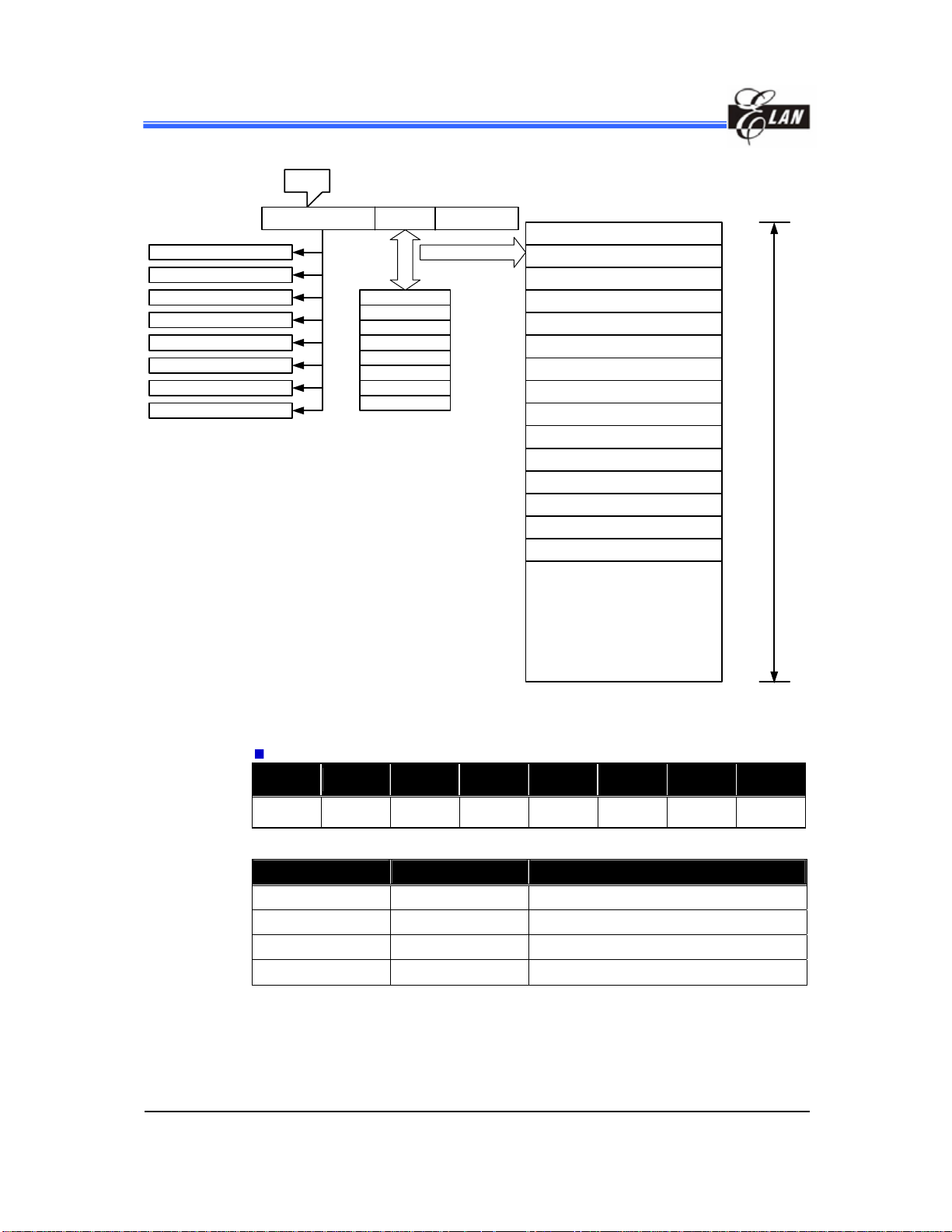
4.1 Functional Block Diagram
OSCI OSCO
WDT timer
Oscillator
Timing Control
R1 (TCC)
Control Sleep and
Wake-up I/O Port
WDT Prescaler
TCC Prescaler
General RAM
R4
DATA a nd CONTRO L BU S
Interrupt
Control
ROM
Instruction
Register
Instruction
Decoder
EM78P809N
8-Bit Microcontroller
Stack
R2
ALU
R3
ACC
R5
TC 2 (16-bit Timer/Counte r)
TC 3 (8-bit Timer/Counter, Capture Mode)
TC 4 (8-bit Timer/Counter, PWM, PDO)
SPI (Serial Periphera l Interface)
UART (Universal Asynchronous
Receiver/Transmitter)
8 channel 10 bit ADC
Keytone
TBT (Time Base Timer)
PORT6
IOC6 R6
P60 ~ P67 P70 ~ P73 P80 ~ P81 P90 ~ P97
PORT7
IOC7 R7
PORT8
IOC8 R8
PORT9
IOC9 R9
Fig. 2. Functional Block Diagram
Product Specification ( V 1 . 0) 07 . 2 6 . 2 005
(This specification is subject to change without further notice)
• 5
Page 10
EM78P809N
8-Bit Microcontroller
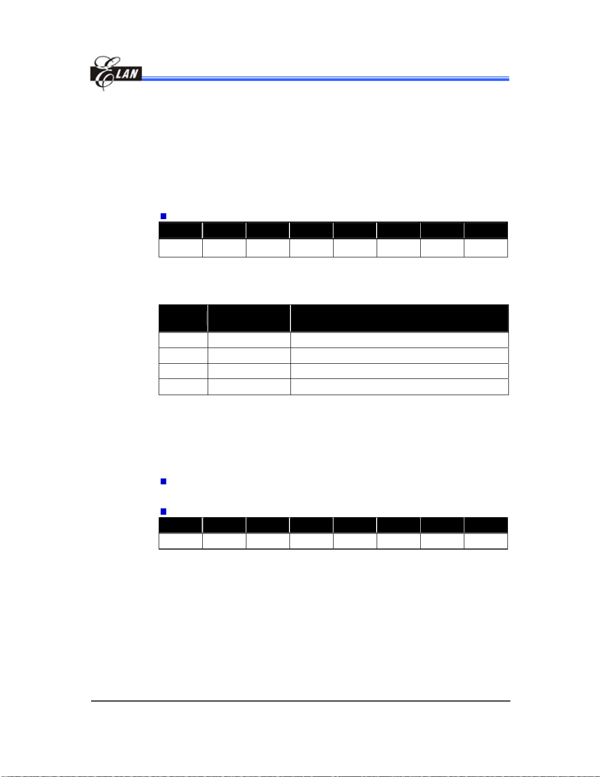
4.2 Operating Registers
Address
00
01
02
03
04
05
06
07
08
09
0A
0B
0C
0D
0E
0F
10
:
1F
REGISTER
BANK 0
R0/ IAR
R1/ TCC
R2/ PC
R3/ SR
R4/ RSR
SCR
PORT6
PORT7
PORT8
PORT9
Reserved
TC4CR
TC4D
ISFR0
ISFR1
ISFR2
16 Byte
Common Register
REGISTER
BANK 1
R3 (7,6)= (0,1)
TC3CR
TC3DA
TC3DB
TC2CR/ ADDL
TC2DH
TC2DL
ADCR
ADIC
ADDH
TBKTC
Reserved
REGISTER
BANK 2
R3 (7,6)= (1,0) R3 (7,6)= (1,1)
URC1
URC2
URS
URRD
URTD
Reserved
Reserved
Reserved
Reserved
Reserved
Reserved
REGISTER
BANK 3
SPIC1
SPIC2
Reserved
Reserved
Reserved
Reserved
SPID
PHC1
PLC1
PHC2
PLC2
CONTROL
REGISTER
Reserved
IOC6
IOC7
IOC8
IOC9
Reserved
INTCR
ADOSCR
Reserved
IMR1
IMR2
20
:
3F
BANK 0
R4 (7,6) = (0,0)
32 Byte
Common Register
BANK 1
R4 (7,6) = (0,1)
32 Byte
Common Register
BANK2
R4 (7,6) = (1,0)
32 Bytes
Common Register
BANK 3
R4 (7,6) = (1,1)
32 Bytes
Common Register
Fig. 3. Operating Registers
Product Specification (V1.0) 07.26.2005
6 •
(This specification is subject to change without further notice)
Page 11

EM78P809N
8-Bit Microcontroller
R0/IAR − Indirect Addressing Register ( Address: 00h )
R0 is not a physically implemented register. Its major function is to act as an indirect
addressing pointer. Any instruction using R0 as a pointer actually accesses data
pointed by the RAM Select Register (R4).
R1/TCC − Time Cloc k /Counter ( Address: 01h )
This register is writable and readable just like the other registers. The contents of the
prescaler counter are cleared only when a value is written into the TCC register.
R2/PC − Program Counter & Stack ( Address: 02h )
Depending on the device type, R2 and hardware stack are 10-bit wide. The
structure is depicted in Fig.4.
Generates 8192 ×13 bits on-chip OTP ROM addresses to the relative
programming instruction codes. One program page is 1024 words long.
R2 is set as all "0"s when under RESET condition
"JMP" instruction allows direct loading of the lower 10 program counter bits.
Thus, "JMP" allows the PC to go to any location within a page.
"CALL" instruction loads the lower 10 bits of the PC, and then PC+1 is
pushed into the stack. Thus, the subroutine entry address can be located
anywhere within a page.
"RET" ("RETL k", "RETI") instruction loads the program counter with the
contents of the top-level stack.
All instructions are single instruction cycle (fclk/2 or fclk/4) except for the
instruction that would change the contents of R2. Such instruction will need
one more instruction cycle.
For an interrupt trigger, the program ROM will jump to individual interrupt
vector at Page 0. The CPU will store ACC, R3 status and R5 PAGE
automatically, it will restore after instruction RETI.
Product Specification ( V 1 . 0) 07 . 2 6 . 2 005
(This specification is subject to change without further notice)
• 7
Page 12
EM78P809N
8-Bit Microcontroller
R5
PC
A12
000 : PAGE0 0000~03FF
001 : PAGE1 0400~07FF
010 : PAGE2 0800~0BFF
011 : PAGE3 0C00~0FFF
100 : PAGE4 1000~13FF
101 : PAGE5 1400~17FF
110 : PAGE6 1800~1BFF
111 : PAGE7 1C00~1FFF
A11 A10 A9 A8 A7 ~ A0
CALL
RET
RETL
RETI
STACK LEVEL 1
STACK LEVEL 2
STACK LEVEL 3
STACK LEVEL 4
STACK LEVEL 5
STACK LEVEL 6
STACK LEVEL 7
STACK LEVEL 8
Store ACC, R3, R5
Reset Vector
WDT Timer Overflow
External INT0 Pin Interrupt Occurs
TCC Overflow
External INT1 pin Interrupt Occurs
Time Base Timer Interrupt
UART Transmit Data Buffer Empty
UART Receive Data Buffer Full
UART Receive Error
TC3 Interrupt
SPI Interrupt
TC4 Interrupt
External INT3 Pin Interrupt Occurs
AD Conversion Complete
External INT5 Pin Interrupt Occurs
On-chip Program Memory
0000h
0003h
0006h
0009h
000Fh
0012h
0015h
0018h
001Bh
0021h
0024h
0027h
0030h
0033h
0036h
User Memory Space
1FFFh
Fig. 4. Program Counter Organiz ation
R3/SR − Status Reg ister ( Address: 03h )
Bit 7 Bit 6 Bit 5 Bit 4 Bit 3 Bit 2 Bit 1 Bit 0
RBS1 RBS0 0 T P Z DC C
Bit 7 ~ Bit 6 (RBS1 ~ RBS0) : R-Register page select
RBS1 RBS0 Register Bank (Address 05H ~ 0FH)
0 0 Bank 0
0 1 Bank 1
1 0 Bank 2
1 1 Bank 3
Bit 5 : Not used
Bit 4 (T) : Time-out bit. Set to “1” with the "SLEP" and "WDTC" commands, or
during power up, and reset to “0” with the WDT time-out.
Product Specification (V1.0) 07.26.2005
8 •
(This specification is subject to change without further notice)
Page 13
EM78P809N
8-Bit Microcontroller
Bit 3 (P) : Power down bit. Set to “1” during power on or by a "WDTC" command
and reset to “0” by a "SLEP" command.
Bit 2 (Z) : Zero flag. Set to "1" if the result of an arithmetic or logic operation is
zero.
Bit 1 (DC) : Auxiliary carry flag
Bit 0 (C) : Carry flag
R4/RSR − RAM Select Register ( Address: 04h )
Bit 7 Bit 6 Bit 5 Bit 4 Bit 3 Bit 2 Bit 1 Bit 0
GRBS1 RBS0 RSR5 RSR4 RSR3 RSR2 RSR1 RSR0
Bit 7: 6 ( GRBS1 : GRBS0 ) : determine which general purpose banks are
activated among the 4 banks. Use BANK instruction (e.g. BABK 1) to
change bank.
GRBS1 GRBS0 General Purpose Register Bank (Address 20H ~ 3FH)
0 0 Bank 0
0 1 Bank 1
1 0 Bank 2
1 1 Bank 3
Bit 5: 0 ( RS R5 : RSR0 ) : are used to select the registers (address: 00h~3Fh) in
the indirect addressing mode. If no indirect addressing is used, the RSR
can be used as an 8-bit general-purpose read/write register. See the
data memory configuration in Fig. 3.
Register Bank 0 ( R3 bits (7, 6) = (0, 0) )
SCR − System Control Register, Program ROM Page Select ( Address: 05h )
Bit 7 Bit 6 Bit 5 Bit 4 Bit 3 Bit 2 Bit 1 Bit 0
0 PS2 PS1 PS0 0 1 SIS REM
Bit 6 (PS2 ) ~ 4 (PS 0) : ROM Page select bits. User can use PAGE instruction (e.g.
PAGE 1) or set PS2~PS0 bits to change the ROM page. When
executing a "JMP", "CALL", or other instructions which cause the
program counter to change (e.g. MOV R2, A), PS2~PS0 are loaded into
the 13th to 11th bits of the program counter and select one of the
available program memory pages. Note that RET (RETL, RETI)
instruction does not change the PS2~PS0 bits. That is, return will
always be to the page from where the subroutine was called, regardless
of the PS2~PS0 bits current setting.
Product Specification ( V 1 . 0) 07 . 2 6 . 2 005
(This specification is subject to change without further notice)
• 9
Page 14
EM78P809N
8-Bit Microcontroller
PS2 PS1 PS0 Program Memory Page [Address]
0 0 0 Page 0 [0000~03FF]
0 0 1 Page 1 [0400~07FF]
0 1 0 Page 2 [0800~0BFF]
0 1 1 Page 3 [0C00~0FFF]
1 0 0 Page 4 [1000~13FF]
1 0 1 Page 5 [1400~17FF]
1 1 0 Page 6 [1800~1BFF]
1 1 1 Page 7 [1C00~1FFF]
Bit 1 ( SIS ) : SLEEP and IDLE mode select.
SIS = “0” : IDLE mode
SIS = “1” : SLEEP mode
Bit 0 ( REM ) : Release method for sleep mode.
REM = “0” : /SLEEP pin input rising edge release
REM = “1” : /SLEEP pin input “H” level release
PORT6 − Port 6 I/O Data Register ( Address: 06h )
Bit 7 Bit 6 Bit 5 Bit 4 Bit 3 Bit 2 Bit 1 Bit 0
P67 P66 P65 P64 P63 P62 P61 P60
Bit 7 ~ Bit 0 ( P67 ~ P60 ) : 8-bits Port 6 I/O data register
User can use IOC6 register to define each bit whether input or output.
PORT7 — Port 7 I/O Data Register ( Address: 07h )
Bit 7 Bit 6 Bit 5 Bit 4 Bit 3 Bit 2 Bit 1 Bit 0
0 0 0 0 P73 P72 P71 P70
Bit 3 ~ Bit 0 ( P73 ~ P70 ) : Port 73 ~ Port 70 I/O data register
User can use IOC7 register to define each bit whether input or output.
PORT8 − Port 8 I/O Data Register ( Address: 08h )
Bit 7 Bit 6 Bit 5 Bit 4 Bit 3 Bit 2 Bit 1 Bit 0
0 0 0 0 0 0 P81 P80
Bit 1 ~ Bit 0 ( P81 ~ P80 ) : Port 81 ~ Port 80 I/O data register
User can use IOC8 register to define input or output each bit.
Product Specification (V1.0) 07.26.2005
10 •
(This specification is subject to change without further notice)
Page 15
EM78P809N
8-Bit Microcontroller
PORT9 − Port 9 I/O Data Register ( Address: 09h )
Bit 7 Bit 6 Bit 5 Bit 4 Bit 3 Bit 2 Bit 1 Bit 0
P97 P96 P95 P94 P93 P92 P91 P90
Bit 7 ~ Bit 0 ( P97 ~ P90 ) : 8-bit Port 97 ~ Port 90 I/O data register
User can use IOC9 register to define each bit whether input or output.
TC4CR — Timer/Counter 4 Control Register ( Address: 0Bh )
Bit 7 Bit 6 Bit 5 Bit 4 Bit 3 Bit 2 Bit 1 Bit 0
TC4FF1 TC4FF0 TC4S TC4CK2 TC4CK1 TC4CK0 TC4M1 TC4M0
Bit 7 ~ Bit 6 ( TC4FF1 ~ TC4FF0 ) : Timer/Counter4 flip-flop control.
TC4FF1 TC4FF0 Operating Mode
0 0 Clear
0 1 Toggle
1 0 Set
1 1 Reserved
Bit 5 ( TC4S ) : Timer/Counter 4 start control.
TC4S = “0” : Stop and clear counter
TC4S = “1” : Start
Bit 4 ~ Bit 2 ( TC4CK2 ~ TC4CK 0 ) : Timer/Counter 4 Clock Source Select
TC4CK2 TC4CK1 TC4CK0
0 0 0 Fc/2^11 250uS 64mS
0 0 1 Fc/2^7 16uS 4mS
0 1 0 Fc/2^5 4uS 1mS
0 1 1 Fc/2^3 1uS 255uS
1 0 0 Fc/2^2 500nS 127.5uS
1 0 1 Fc/2^1 250nS 63.8uS
1 1 0 Fc 125nS 31.9uS
1 1 1 External clock (TC4 pin) -- --
Clock Source
( Normal, Idle )
Resolution
( Fosc=8M )
Max. Time
( Fosc=8M )
Bit 1 ~ Bit 0 ( TC4M1 ~ TC4M0 ) : Timer/Counter 4 Operating Mode Select
TC4M1 TC4M0 Operating Mode
0 0 Timer/Counter
0 1 Reserved
1 0 Programmable Divider output
1 1 Pulse Width Modulation output
Product Specification ( V 1 . 0) 07 . 2 6 . 2 005
(This specification is subject to change without further notice)
• 11
Page 16
EM78P809N
8-Bit Microcontroller
TC4D − Timer 4 Data Buffer ( Address: 0Ch )
Bit 7 Bit 6 Bit 5 Bit 4 Bit 3 Bit 2 Bit 1 Bit 0
TC4D7 TC4D6 TC4D5 TC4D4 TC4D3 TC4D2 TC4D1 TC4D0
ISFR0 − Interrupt Status Flag Register 0 and INT3 Edge Detect Flag.
Bit 7 Bit 6 Bit 5 Bit 4 Bit 3 Bit 2 Bit 1 Bit 0
Bit 7 ~ Bit 0 ( TC4D7 ~ TC4D0 ) : Data buffer of 8-bit Timer/Counter 4.
( Address : 0Dh )
0 0 INT3F INT3R 0 0 WDTIF EXIF0
Bit 5 ( INT3F ) : External interrupt 3 falling edge detect flag.
INT3F = “0” : Falling edge is not detected
INT3F = “1” : Falling edge is detected
Bit 4 ( INT3R ) : External interrupt 3 rising edge detect flag.
INT3 R = “0” : Rising edge is not detected
INT3 R = “1” : Rising edge is detected
Bit 1 ( WDTIF ) : WDT time-out flag, flag cleared by software.
Bit 0 ( EXIF0 ) : External interrupt flag (INT0). Flag cleared by software. If the
INT0EN is reset to “0”, the flag is cleared.
ISFR1 − Interrupt Status Flag Register 1 ( Address: 0Eh )
Bit 7 Bit 6 Bit 5 Bit 4 Bit 3 Bit 2 Bit 1 Bit 0
EXIF5 TCIF2 ADIF 0 EXIF3 TCIF4 SPIF TCIF3
Bit 7 ( EXIF5 ) : External Interrupt Flag (/INT5), flag cleared by software.
Bit 6 ( TCIF2 ) : 16-bit Timer/Counter 2 Interrupt Flag, flag cleared by software.
Bit 5 ( ADIF ) : AD conversion complete flag, flag cleared by software.
Bit 3 ( EXIF3 ) : External Interrupt Flag (/INT3), flag cleared by software.
Bit 2 ( TCIF4 ) : 8-bit Timer/Counter 4 Interrupt Flag, flag cleared by software.
Bit 1 ( SPIF ) : SPI Mode Interrupt Flag, flag cleared by software.
Bit 0 ( TCIF3 ) : 8-bit Timer/Counter 3 interrupt flag, flag cleared by software.
"1" means interrupt request, "0" means non-interrupt
ISFR1 can be cleared by instruction, but cannot be set by instruction
IMR1 is the interrupt mask register
Note that reading ISFR1 will obtain the result of the ISFR1 "logic AND" and
IMR1.
Product Specification (V1.0) 07.26.2005
12 •
(This specification is subject to change without further notice)
Page 17

EM78P809N
8-Bit Microcontroller
ISFR2 − Interrupt Status Flag Register 2 ( Address: 0Fh )
Bit 7 Bit 6 Bit 5 Bit 4 Bit 3 Bit 2 Bit 1 Bit 0
0 UERRIF RBFF TBEF TBIF EXIF1 0 TCIF0
Bit 6 (UERRIF) : UART Receiving Error Interrupt, cleared by software or UART
disabled.
Bit 5 (RBFF) : UART Receive Mode Data Buffer Full Interrupt Flag. Flag cleared
by software.
Bit 4 (TBEF) : UART Transmit Mode Data Buffer Empty Interrupt Flag. Flag
cleared by software.
Bit 3 (TBIF) : Time Base Timer Interrupt Flag. Flag cleared by software.
Bit 2 (EXIF1) : External Interrupt Flag (INT1). Flag cleared by software.
Bit 0 (TCIF0) : TCC Overflow Interrupt Flag. Set as TCC overflows; flag cleared
by software.
"1" means interrupt request, "0" means non-interrupt
ISFR2 can be cleared by instruction, but cannot be set by instruction
IMR2 is the interrupt mask register
Note that reading ISFR2 will obtain the result of the ISFR2 "logic AND" and
IMR2
Register Bank 1 ( R3 bits ( 7,6) = (0,1) )
TC3CR − Timer/Counter 3 Control Register ( Address: 05h )
Bit 7 Bit 6 Bit 5 Bit 4 Bit 3 Bit 2 Bit 1 Bit 0
TC3CAP TC3S TC3CK1 TC3CK0 TC3M 0 0 0
Bit 7 ( TC3CAP ) : Software capture control
TC3CAP = “0” : -
TC3CAP = “1” : Software capture
Bit 6 ( TC3S ) : Timer/Counter 3 start control
TC3S = “0” : Stop and counter clear
TC3S = “1” : Start
Product Specification ( V 1 . 0) 07 . 2 6 . 2 005
(This specification is subject to change without further notice)
• 13
Page 18
EM78P809N
8-Bit Microcontroller
TC3CK1 TC3CK0
TC3DA − Timer 3 Data Buffer A ( Address: 06h )
Bit 7 Bit 6 Bit 5 Bit 4 Bit 3 Bit 2 Bit 1 Bit 0
TC3DA7 TC3DA6 TC3DA5 TC3DA4 TC3DA3 TC3DA2 TC3DA1 TC3DA0
Bit 5 ~ Bit 4 ( TC3CK1 ~ TC3CK0 ) : Timer/Counter3 Clock Source Select
Clock source
( Normal, Idle )
0 0 Fc/212 512μS 131.1mS
0 1 Fc/210 128μS 32.6mS
1 0 Fc/27 16μS 4.1mS
1 1 External clock (TC3 pin) - -
Resolution
( Fc=8M )
Max. time
( Fc=8M )
Bit 3 ( TC3M ) : Timer/Counter 3 mode select
TC3M = “0” : Timer/Counter3 mode
TC3M = “1” : Capture mode
Bit 7 ~ Bit 0 ( TC3DA7 ~ TC3DA0 ) : Data buffer of 8-bit Timer/Counter 3.
Reset does not affect this register.
TC3DB − Timer 3 Data Buffer B ( Addres s: 07h )
Bit 7 Bit 6 Bit 5 Bit 4 Bit 3 Bit 2 Bit 1 Bit 0
TC3DB7 TC3DB6 TC3DB5 TC3DB4 TC3DB3 TC3DB2 TC3DB1 TC3DB0
Bit 7 ~ Bit 0 ( TC3DB7 ~ TC3DB0 ) : Data buffer of 8-bit Timer/Counter 3
Reset does not affect this register.
TC2CR/ ADDL — Timer/Counter 2 Control Register, AD Low 2 bits Data
Buffer ( A d dress: 08h )
Bit 7 Bit 6 Bit 5 Bit 4 Bit 3 Bit 2 Bit 1 Bit 0
ADD1 ADD0 0 TC2M TC2S TC2CK2 TC2CK1 TC2CK0
Bit 7 ~ Bit 6 ( ADD1 ~ ADD0 ) : AD low 2-bit data buffer
Bit 4 ( TC2M ) : Timer/Counter 2 mode select
TC2M = “0” : Timer/counter mode
TC2M = “1” : Window mode
Bit 3 ( TC2S ) : Timer/Counter 2 start control
TC2S = “0” : Stop and counter clear
TC2S = “1” : Start
Product Specification (V1.0) 07.26.2005
14 •
(This specification is subject to change without further notice)
Page 19
EM78P809N
8-Bit Microcontroller
Bit 2 ~ Bit 0 ( TC2CK2 ~ TC2CK0 ) : Timer/Counter 2 Clock Source Select
TC2CK2 TC2CK1 TC2CK0
0 0 0 Fc/223 1.05s 19.1h
0 0 1 Fc/213 1.02ms 1.1min
0 1 0 Fc/28 32μs 2.1s
0 1 1 Fc/23 1μs 65.5ms
1 0 0 Fc 125ns 7.9ms
1 0 1 - - -
1 1 0 - - -
1 1 1 External clock (TC2 pin)
Clock Source
( Normal, Idle )
Resolution
( Fc=8M )
Max. Time
( Fc=8M )
TC2DH − Timer 2 Data Buffer High Byte ( Address: 09h )
Bit 7 Bit 6 Bit 5 Bit 4 Bit 3 Bit 2 Bit 1 Bit 0
TC2D15 TC2D14 TC2D13 TC2D12 TC2D11 TC2D10 TC2D9 TC2D8
Bit 7 ~ Bit 0 ( TC2D15 ~ TC2D8 ) : 16-bit Timer/Counter 2 data buffer high byte.
TC2DL − Timer 2 Data Buffer Low Byte ( Address: 0Ah )
Bit 7 Bit 6 Bit 5 Bit 4 Bit 3 Bit 2 Bit 1 Bit 0
TC2D7 TC2D6 TC2D5 TC2D4 TC2D3 TC2D2 TC2D1 TC2D0
Bit 7 ~ Bit 0 ( TC2D7 ~ TC2D0 ) : 16-bit Timer/Counter 2 data buffer low byte.
ADCR − AD Control Register ( Address: 0Bh )
Bit 7 Bit 6 Bit 5 Bit 4 Bit 3 Bit 2 Bit 1 Bit 0
ADREF ADRUN ADCK1 ADCK0 ADP ADIS2 ADIS1 ADIS0
Bit 7 ( ADREF ) : AD reference voltage input select.
ADREF = “0” : Internal VDD, P97 is used as IO.
ADREF = “1” : External reference pin, P97 is used as reference input pin.
Bit 6 ( ADRUN ) : AD Conversion start
ADRUN = “0” : Reset on completion of the conversion by hardware, this bit
cannot be reset by software.
ADRUN = “1” : Conversion starts
Product Specification ( V 1 . 0) 07 . 2 6 . 2 005
(This specification is subject to change without further notice)
• 15
Page 20
EM78P809N
8-Bit Microcontroller
Bit 5~ Bit 4 ( ADCK1 ~ ADCK0 ) : AD Conversion Time Select
ADCK1 ADCK0
0 0 Fc/4 1MHz
0 1 Fc/16 4MHz
1 0 Fc/32 8MHz
1 1 Reserved -
Clock Source
( Normal, Idle )
Max. Op erating
Frequency (Fc)
Bit 3 ( ADP ) : AD power control
ADP = “0” : Power on
ADP = “1” : Power down
Bit 2 ~ Bit 0 ( ADIS2 ~ ADIS0 ) : Analog Input Pin Select
ADIS2 ADIS1 ADIS0 Analog Input Pin
0 0 0 AD0
0 0 1 AD1
0 1 0 AD2
0 1 1 AD3
1 0 0 AD4
1 0 1 AD5
1 1 0 AD6
1 1 1 AD7
ADIC − AD Input Pin Control ( Address: 0Ch )
Bit 7 Bit 6 Bit 5 Bit 4 Bi t 3 Bit 2 Bit 1 Bit 0
ADE7 ADE6 ADE5 ADE4 ADE3 ADE2 ADE1 ADE0
Bit 7 ~ Bit 0 ( ADE7 ~ ADE0 ) : AD input pin enable control.
ADEx = “0” : PORT9.x act as I/O pin.
ADEx = “1” : PORT9.x act as analog input pin.
ADDH − AD High 8-bit Data Buffer ( Address: 0Dh )
Bit 7 Bit 6 Bit 5 Bit 4 Bit 3 Bit 2 Bit 1 Bit 0
ADD9 ADD8 ADD7 ADD6 ADD5 ADD4 ADD3 ADD2
Bit 7 ~ Bit 0 ( ADD9 ~ ADD2 ) : AD high 8-bit data buffer.
Product Specification (V1.0) 07.26.2005
16 •
(This specification is subject to change without further notice)
Page 21
EM78P809N
8-Bit Microcontroller
TBKTC − TBT/Keytone Control ( Address: 0Eh )
Bit 7 Bit 6 Bit 5 Bit 4 Bit 3 Bit 2 Bit 1 Bit 0
TEN TCK1 TCK0 0 TBTEN TBTCK2 TBTCK1 TBTCK0
Bit 7 ( TEN ) : Keytone enable control
TEN = “0” : Disable
TEN = “1” : Enable
Bit 6 ~ Bit 5 ( TCK1 ~ TCK0 ) : Keytone Output Clock Source Select
TCK1 TCK0
0 0 Fc/213 0.976kHz
0 1 Fc/212 1.953kHz
1 0 Fc/211 3.906kHz
1 1 Fc/210 7.812kHz
Clock Source
( Normal, Idle )
Bit 3 ( TBTEN ) : Time Base Timer Enable Control
TBTEN = “0” : Disable
Keytone Output Frequency
( Fc = 8MHz )
TBTEN = “1” : Enable
Bit 2 ~ Bit 0 ( TBTCK2 ~ TBTCK0 ) : Time Base Timer Clock Source Select
TBTCK2 TBTCK1 TBTCK0
0 0 0 Fc/223 0.95Hz
0 0 1 Fc/221 3.81Hz
0 1 0 Fc/216 122.07Hz
0 1 1 Fc/214 488.28Hz
1 0 0 Fc/213 976.56Hz
1 0 1 Fc/212 1953.12Hz
1 1 0 Fc/211 3906.25Hz
1 1 1 Fc/29 15625Hz
Register Bank 2 ( R3 bits (7, 6) = (1, 0) )
URC1 − UART Control Register 1 ( Address: 05h )
Bit 7 Bit 6 Bit 5 Bit 4 Bit 3 Bit 2 Bit 1 Bit 0
URTD8 UMODE1 UMODE0 BRATE2 BRATE1 BRATE0 UTBE TXE
Clock Source
( Normal, Idle )
Interrupt Frequency
( Fc = 8MHz )
Bit 7 ( URTD8 ) : Transmission data bit 8
Product Specification ( V 1 . 0) 07 . 2 6 . 2 005
(This specification is subject to change without further notice)
• 17
Page 22
EM78P809N
8-Bit Microcontroller
Bit 6 ~ Bit 5 ( UMODE1 ~ UMODE0 ) : UART Transmission Mode Select Bit
UMODE1 UMODE0 UART Mode
0 0 Mode1: 7-bits
0 1 Mode2: 8-bits
1 0 Mode3: 9-bits
1 1 Reserved
Bit 4 ~ Bit 2 ( BRAT E2 ~ BRATE1 ) : Transmit Baud Rate Select
BRATE2 BRATE1 BRATE0 Baud Rate e.g. Fc=8MH z
0 0 0 Fc/13 38400
0 0 1 Fc/26 19200
0 1 0 Fc/52 9600
0 1 1 Fc/104 4800
1 0 0 Fc/208 2400
1 0 1 Fc/416 1200
1 1 0 TC4
1 1 1 Fc/96
Bit 1 ( UTBE ) : UART transfer buffer empty flag. Set to 1 when transfer buffer is
empty. Reset to 0 automatically when writing into the URTD register. UTBE bit will
be cleared by hardware when enabling the transmission. UTBE bit is read-only.
Therefore, writing to the URTD register is necessary when we want to start
transmission shifting.
Bit 0 ( TXE ) : Enable transmission
TXE = “0” : Disable
TXE = “1” : Enable
URC2 − UART Control Register 2 ( Address: 06h )
Bit 7 Bit 6 Bit 5 Bit 4 Bit 3 Bit 2 Bit 1 Bit 0
0 0 SBIM1 SBIM0 UINVEN 0 0 0
Bit 5 ~ Bit 4 ( SBIM1 ~ SBIM0 ) : Serial bus interface operation mode select.
TC2CK1 TC2CK0 Operation Mode
0 0 I/O mode
0 1 SPI mode
1 0 UART mode
1 1 Reserved
Bit 3 ( UINVEN ) : Enable UART TXD and RXD port inverse output.
UINVEN = “0” : Disable TXD and RXD port inverse output.
UINVEN = “1” : Enable TXD and RXD port inverse output.
Product Specification (V1.0) 07.26.2005
18 •
(This specification is subject to change without further notice)
Page 23

EM78P809N
8-Bit Microcontroller
URS − UART Status Register ( Address: 07h )
Bit 7 Bit 6 Bit 5 Bit 4 Bit 3 Bit 2 Bit 1 Bit 0
URRD8 EVEN PRE PRERR OVERR FMERR URBF RXE
Bit 7 ( URRD8 ) : Receiving data bit 8
Bit 6 ( EVEN ) : Select parity check
EVEN = “0” : Odd parity
EVEN = “1” : Even parity
Bit 5 ( PRE ) : Enable parity addition
PRE = “0” : Disable
PRE = “1” : Enable
Bit 4 ( PRERR ) : Parity error flag.
Set to 1 when parity error occurred, and cleared to 0 by software.
Bit 3 ( OVERR ) : Overrun error flag.
Set to 1 when overrun error occurred, and cleared to 0 by software.
Bit 2 ( FMERR ) : Framing error flag.
Set to 1 when framing error occurred, and cleared to 0 by software.
Bit 1 ( URBF ) : UART read buffer full flag.
Set to 1 when one character is received. Reset to 0 automatically when read
from the URS register. URBF will be cleared by hardware when receiving is
enabled. URBF bit is read-only. Therefore, reading the URS register is
necessary to avoid an overrun error.
Bit 0 ( RXE ) : Enable receiving
RXE = “0” : Disable
RXE = “1” : Enable
URRD − UART Receive Data Buffer ( Address: 08h )
Bit 7 Bit 6 Bit 5 Bit 4 Bit 3 Bit 2 Bit 1 Bit 0
URRD7 URRD6 URRD5 URRD4 URRD3 URRD2 URRD1 URRD0
Bit 7 ~ Bit 0 ( URRD7 ~ URRD0 ) : UART receive data buffer. Read only.
Product Specification ( V 1 . 0) 07 . 2 6 . 2 005
(This specification is subject to change without further notice)
• 19
Page 24

EM78P809N
8-Bit Microcontroller
URTD − UART Tr ansmit Data Buffer ( Address: 09h )
Bit 7 Bit 6 Bit 5 Bit 4 Bi t 3 Bit 2 Bit 1 Bit 0
URTD 7 URTD 6 URTD 5 URTD 4 URTD 3 URTD 2 URTD 1 URTD0
Register Bank 3 ( R3 bits ( 7,6) = (1,1) )
SPIC1 − SPI Control Register 1 ( Address: 05h )
Bit 7 Bit 6 Bit 5 Bit 4 Bit 3 Bit 2 Bit 1 Bit 0
SMP DCOL BRS2 BRS1 BRS0 EDS DORD WBE
In using external clock, data input sample is fixed at the middle of data output time.
Bit 7 ~ Bit 0 ( UR TD 7 ~ URTD 0) : UART transmit data buffer. Write only.
Bit 7 ( SMP ) : SPI data input sample phase.
SMP = “0” : Input data sampled at middle of data output time
SMP = “1” : Input data sampled at the end of data output time
Bit 6 ( DCOL ) : SPI Data collision.
DCOL = “0” : Data collision didn’t occur
DCOL = “1” : Data collision occurred. It should be cleared by software.
Bit 5 ~ Bit 3 ( BRS0 ~ BRS2 ) : SPI Clock Source Select
BRS2 BRS1 BRS0
0 0 0 Fc/213 0.95Kbit/s
0 0 1 Fc/211 3.8Kbit/s
0 1 0 Fc/210 7.6Kbit/s
0 1 1 Fc/28 30.5Kbit/s
1 0 0 Fc/26 122Kbit/s
1 0 1 Fc/25 244Kbit/s
1 1 0 External clock (/SCK pin) -
1 1 1 External clock (/SCK pin) -
Clock Source
( Normal, Idle )
Max. Transfer Rate
( Fc = 8MHz )
Bit 2 ( EDS ) : Data shift out edge select.
EDS = “0” : Rising edge
EDS = “1” : Falling edge
Bit 1 ( DORD ) : Data transmission order.
DORD = “0” : Shift left (MSB first)
DORD = “1” : Shift right (LSB first)
Product Specification (V1.0) 07.26.2005
20 •
(This specification is subject to change without further notice)
Page 25

EM78P809N
8-Bit Microcontroller
Bit 0 ( WBE ) : Write buffer empty flag. Read only.
WBE = “0” : Write buffer empty
WBE = “1” : Not empty, set to “1” automatically when writing data to the data
buffer.
SPIC2 − SPI Control Register 2 (Address : 06h )
Bit 7 Bit 6 Bit 5 Bit 4 Bit 3 Bit 2 Bit 1 Bit 0
SPIS 0 0 0 0 SPIM1 SPIM0 RBF
Bit 7 ( SPIS ) : SPI start shift, set the bit to “1” and shift register starts to shift. It is
cleared by hardware when shifting is finished. In transferring the
next data, it must be set to “1” again.
S PIS = “0” : Shift finish
S PIS = “1” : Shift starts
Bit 2 ~ Bit 1 ( SPIM1 ~ SPIM0) : SPI Transfer Mode Select
TC2CK1 TC2CK0 Transfer Mode
0 0 8-bit Transmit/Receive mode
0 1 8-bit Transmit mode
1 0 8-bit Receive mode
1 1 Reserved
Bit 0 ( RBF ) : Set to 1 by Buffer Full Detector, and cleared to 0 automatically when
reading data from the SPID register. RBF bit will be cleared by
hardware when enabling SPI. And RBF bit is read-only. Therefore,
reading the SPRL register is necessary to avoid data collision to
occur (DCOL).
SPID (SPI Data Buffer ( Address: 07h )
Bit 7 Bit 6 Bit 5 Bit 4 Bit 3 Bit 2 Bit 1 Bit 0
SPID7 SPID6 SPID5 SPID4 SPID3 SPID2 SPID1 SPID0
Bit 7 ~ Bit 0 ( SPID7 ~ SPID0 ) : SPI data buffer.
PHC1 − Pull High Control Register 1 ( Address: 0Ah )
Bit 7 Bit 6 Bit 5 Bit 4 Bit 3 Bit 2 Bit 1 Bit 0
- - /PHE81 /PHE80 /PHE63 /PHE62 /PHE61 /PHE60
Bit 5 ~ 4 ( /PHE81 ~ /PHE80 ) : bits 1, 0 of Port 8 Pull high enable bit
/PHE8x = “0” : Enable P8x pull high
/PHE8x = “1” : Disable P8x pull high
Product Specification ( V 1 . 0) 07 . 2 6 . 2 005
(This specification is subject to change without further notice)
• 21
Page 26

EM78P809N
8-Bit Microcontroller
PLC1 (Pull Low Control Register 1 ( Address : 0Bh )
Bit 7 Bit 6 Bit 5 Bit 4 Bit 3 Bit 2 Bit 1 Bit 0
Bit 3 ~ 0 ( /PHE63 ~ /PHE60 ) : bit 3 ~ 0 of Port 6 Pull high enable bit
/PHE6x = “0” : Enable P6x pull high
/PHE6x = “1” : Disable P6x pull high
- - /PLE81 /PLE80 /PLE63 /PLE62 /PLE61 /PLE60
Bit 5 ~ 4 ( /PLE81 ~ /PLE80 ) : bits 1, 0 of Port 8 Pull low enable bit
/PLE8x = “0” : Enable P8x pull low
/PLE8x = “1” : Disable P8x pull low
Bit 3 ~ 0 ( /PLE 63 ~ /PLE60 ) : bits 3 ~ 0 of Port 6 Pull low enable bit
/PLE6x = “0” : Enable P6x pull low
/PLE6x = “1” : Disable P6x pull low
PHC2 − Pull High Control Register 2 ( Address: 0Ch )
Bit 7 Bit 6 Bit 5 Bit 4 Bit 3 Bit 2 Bit 1 Bit 0
- - - - /PHE73 /PHE72 /PHE71 /PHE70
Bit 3 ~ 0 ( /PHE73 ~ /PHE70 ) : bits 3 ~ 0 of Port 7 Pull high enable bit
/PHE7x = “0” : Enable P7x pull high
/PHE7x = “1” : Disable P7x pull high
PLC2 − Pull Low Control 2 ( Address: 0Dh )
Bit 7 Bit 6 Bit 5 Bit 4 Bit 3 Bit 2 Bit 1 Bit 0
- - - - /PLE73 /PLE72 /PLE71 /PLE70
Bit 3 ~ 0 ( /PLE 73 ~ /PLE70 ) : bits 3 ~ 0 of Port 7 Pull low enable bit
/PLE7x = “0” : Enable P7x pull low
/PLE7x = “1” : Disable P7x pull low
R10~R1F and R20~R3F (including Banks 0~3) are General Purpose Register
Product Specification (V1.0) 07.26.2005
22 •
(This specification is subject to change without further notice)
Page 27

4.3 Special Purpose Registers
A (Accumulator)
Internal data transfer, or instruction operand holding.
It cannot be addressed.
CONT (Control Register)
Bit 7 Bit 6 Bit 5 Bit 4 Bit 3 Bit 2 Bit 1 Bit 0
WDTO /INT WDTP1 WDTP0 WDTE PSR2 PSR1 PSR0
CONT register is both readable and writable.
Bit 7 ( WDTO ) : WDT output select
WDTO = “0” : Interrupt request
WDTO = “1” : Internal reset
Bit 6 ( /INT ) : Interrupt enable flag
/INT = “0” : masked by DISI or hardware interrupt
EM78P809N
8-Bit Microcontroller
/INT = “1” : enabled by ENI/RETI instructions
Bit 5 ~ Bit 4 ( WDTP1 ~ WDTP0 ) : WDT prescaler bits.
WDTP1 WDTP0 Operating Mode
0 0 1:4
0 1 1:16
1 0 1:64
1 1 1:256
Bit 3 ( WDTE ) : WDT enable control.
WDTE = “0” : Disable
WDTE = “1” : Enable
Bit 2 ( PSR2 ) ~ Bit 0 ( PSR0 ) : TCC prescaler bits.
PSR2 PSR1 PSR0 Operating Mode
0 0 0 1:2
0 0 1 1:4
0 1 0 1:8
0 1 1 1:16
1 0 0 1:32
1 0 1 1:64
1 1 0 1:128
1 1 1 1:256
Product Specification ( V 1 . 0) 07 . 2 6 . 2 005
(This specification is subject to change without further notice)
• 23
Page 28

EM78P809N
8-Bit Microcontroller
IOC6 ~ IOC9 − I/ O Port Control Register
INTCR − INT Control Register ( Address : 0Bh )
Bit 7 Bit 6 Bit 5 Bit 4 Bit 3 Bit 2 Bit 1 Bit 0
INT1NR INT0EN 0 INT3ES1 INT3ES0 0 INT1ES TC2ES
"1" puts the relative I/O pin into high impedance, while "0" defines the relative
I/O pin as output.
IOC6 and IOC9 registers are both readable and writable.
Bit 7 ( INT 1NR ) : INT1 noise reject time select
INT1NR = “0” : Pulses less than 63/fc are eliminated as noise
INT1NR = “1” : Pulses less than 15/fc are eliminated as noise
Bit 6 ( INT0EN ) : INT0 enable control
INT0EN = “0” : General I/O
INT0EN = “1” : /INT0 pin
Bit 5 : Reserved
Bit 4 ~ Bit 3 ( INT3ES1 ~ IN T3ES0) : INT3 edge select
INT3ES1 INT3ES0 Edge Select
0 0 Rising
0 1
1 0
1 1
Falling
Both edge
Reserved
Bit 2 : Reserved
Bit 1 ( INT1ES ) : INT1 edge select
INT1ES = “0” : Rising edge
INT1ES = “1” : Falling edge
Bit 0 (TC2ES) : Timer/Counter 2 edge select.
TC2ES = “0” : Rising edge
TC2ES = “1” : Falling edge
Product Specification (V1.0) 07.26.2005
24 •
(This specification is subject to change without further notice)
Page 29

EM78P809N
8-Bit Microcontroller
External Interrupt
INT Pin
/INT0 P60 ENI + INT0EN (IOCB) Falling -
INT1 P61 ENI + EXIE1 (IMR2) Rising or Falling 15/Fc, 63/Fc
INT3 P80, TC3 ENI + EXIE3 (IMR2)
/INT5 P73, /SLEEP ENI + EXIE5 (IMR2)
Secondary
Function Pin
Enable Condition Edge
Rising or Falling or
Rising/Falling
-
ADOSCR − AD Offset Control Register ( Address : 0Ch )
Bit 7 Bit 6 Bit 5 Bit 4 Bit 3 Bit 2 Bit 1 Bit 0
CALI SIGN VOF[2] VOF[1] VOF[0] 0 0 0
Bit 7 (CALI) : Calibration enable bit for A/D offset
CALI = “0” : Calibration disable
CALI = “1” : Calibration enable
Bit 6 ( SIGN ) : Polarity bit of offset voltage
Digital Noise
Reject
7/Fc
SIGN = “0” : Negative voltage
SIGN = “1” : Positive voltage
Bit 5 ~ Bit 3 ( VOF[2] ~ VOF[0] ) : Offset voltage bits
IMR1 − Interrupt Mask Register 1 ( Address : 0Eh )
Bit 7 Bit 6 Bit 5 Bit 4 Bit 3 Bit 2 Bit 1 Bit 0
EXIE5 TCIE2 ADIE 0 EXIE3 TCIE4 SPIE TCIE3
Bit 7 ( EXIE5 ) : External/INT5 pin Interrupt enable bit.
EXIE5 = “0” : disable EXIF5 interrupt
EXIE5 = “1” : enable EXIF5 interrupt
Bit 6 ( TCIE2 ) : Timer/Counter 2 Interrupt enable bit.
TCIE2 = “0” : disable TCIF2 interrupt
TCIE2 = “1” : enable TCIF2 interrupt
Bit 5 ( ADIE ) : ADC complete interrupt enable bit.
ADIE = “0” : disable ADIF interrupt
ADIE = “1” : enable ADIF interrupt
Product Specification ( V 1 . 0) 07 . 2 6 . 2 005
(This specification is subject to change without further notice)
• 25
Page 30

EM78P809N
8-Bit Microcontroller
Bit 3 ( EXIE3 ) : External INT3 pin Interrupt enable bit.
EXIE3 = “0” : disable EXIF3 interrupt
EXIE3 = “1” : enable EXIF3 interrupt
Bit 2 ( TCIE4 ) : Timer/Counter 4 Interrupt enable bit.
TCIE4 = “0” : disable TCIF4 interrupt
TCIE4 = “1” : enable TCIF4 interrupt
Bit 1 ( SPIE ) : SPI Interrupt enable bit.
SPIE = “0” : disable SPIF interrupt
SPIE = “1” : enable SPIF interrupt
Bit 0 ( TCIE3 ) : Timer/Counter 3 Interrupt enable bit.
TCIE3 = “0” : disable TCIF3 interrupt
TCIE3 = “1” : enable TCIF3 interrupt
Individual interrupt is enabled by setting its associated control bit in the IMR1
to "1".
Global interrupt is enabled by the ENI instruction and is disabled by the DISI
instruction.
IMR1 register is both readable and writable.
IMR2 − Interrupt Mask Register 2( Address: 0Fh )
Bit 7 Bit 6 Bit 5 Bit 4 Bit 3 Bit 2 Bit 1 Bit 0
0 UERRIE URIE UTIE TBIE EXIE1 0 TCIE0
Bit 6 ( UERRIE ) : UART receive error interrupt enable bit.
UERRIE = “0” : disable UERRIF interrupt
UERRIE = “1” : enable UERRIF interrupt
Bit 5 ( URIE ) : UART receive mode interrupt enable bit.
URIE = “0” : disable RBFF interrupt
URIE = “1” : enable RBFF interrupt
Bit 4 ( UTIE ) : UART transmit mode interrupt enable bit.
UTIE = “0” : disable TBEF interrupt
UTIE = “1” : enable TBEF interrupt
Product Specification (V1.0) 07.26.2005
26 •
(This specification is subject to change without further notice)
Page 31

EM78P809N
8-Bit Microcontroller
Bit 3 ( TBIE ) : Time base timer interrupt enable bit.
TBIE = “0” : disable TBIF interrupt
TBIE = “1” : enable TBIF interrupt
Bit 2 ( EXIE1 ) : External INT 1 Interrupt enable bit.
EXIE1 = “0” : disable EXIF1 interrupt
EXIE1 = “1” : enable EXIF1 interrupt
Bit 0 ( TCIE0 ) : TCC Interrupt enable bit.
TCIE0 = “0” : disable TCIF0 interrupt
TCIE0 = “1” : enable TCIF0 interrupt
Individual interrupt is enabled by setting its associated control bit in the IMR2
to "1".
Global interrupt is enabled by the ENI instruction and is disabled by the DISI
instruction.
IMR2 register is both readable and writable.
4.4 CPU Operation Mode
Registers for CPU operation mode
R_BANK Address NAME Bit 7 Bit 6 Bit 5 Bit 4 Bit 3 Bit 2 Bit 1 Bit 0
BANK 0 0X05 SCR 0 PS2 PS1 PS0 0 1 SIS REM
-- R/W R/W R/W -- -- R/W R/W
* R_BANK: Register Bank (bits 7, 6 of R3), R/W: Read/Write
SIS=0 + SLEP
IDLE MODE
CPU : Halts
Fosc: Oscillates
Interrupt
Fig 5. Operation Mod e and S wit ch in g
Reset Occurs
NORMAL MODE
CPU : Operating
Fosc: Oscillates
SIS=1 + SLEP
SLEEP MODE
CPU : Halts
Fosc: Stops
/SLEEP Pin Input
Product Specification ( V 1 . 0) 07 . 2 6 . 2 005
(This specification is subject to change without further notice)
• 27
Page 32

EM78P809N
8-Bit Microcontroller
Table 2. Mode Switching Control
Table 3. Operation Mode
Signal
Clock
In NORMAL mode, the CPU core and on-chip peripherals operate in oscillator
frequency.
In IDLE mode, the CPU core halts, but the on-chip peripheral and oscillator circuit
remain active. IDLE mode is released to NORMAL mode by any interrupt source. If the
ENI instruction is set, an interrupt will be serviced first followed by executing the next
instruction which is after the IDLE mode is released and the interrupt service is finished.
If the ENI instruction is not set, the next instruction will be executed which is after the
IDLE mode start instruction. IDLE mode can also be released by setting the /RESET
pin to low and executing a reset operation.
Mode Switch Switch Method Note
Normal Æ Sleep Set SIS = 1, execute SLEP instruction
Sleep Æ Normal /SLEEP pin wake up
Normal Æ Idle Set SIS = 0, execute SLEP instruction
Idle Æ Normal Interrupt
Operation Mode Frequency CPU Code
Reset Reset Reset
Normal Fosc
Idle
Sleep Turn off
Turn on
Halt
On-chip
Peripherals
Fosc
Halt
In SLEEP mode, the internal oscillator is turned off and all system operation is halted.
SLEEP mode is released by /SLEEP pin (level sensitive or edge sensitive can be set by
System Control Register (SCR) bit 0 (REM)). After a warm-up period, the next
instruction will be executed which is after the SLEEP mode start instruction. SLEEP
mode can also be released by setting the /RESET pin to low and executing a reset
operation. In level sensitive mode, the /SLEEP pin must be confirmed in low level
before entering SLEEP mode. In edge sensitive mode, SLEEP mode is started even
when the /SLEEP pin is in high level.
Table 4. Wake-up Methods
SLEEP Mode
Wake-up Signal
1. Individual interrupt source
in IMR1, IMR2
2. WDT interrupt request
3. /INT0
4. ENI instruction is not
executed
Product Specification (V1.0) 07.26.2005
28 •
(This specification is subject to change without further notice)
R5 (SIS) = 1+SLEP
Instruction
No effect
(**)
IDLE Mode
R5 (SIS)= 0 + SLEP
Instruction
1. Wake-up
2. Jump to the next
instruction or enter
IDLE mode
NORMAL
Mode
R5 (SIS)=(*)
No effect
(**)
Page 33

EM78P809N
8-Bit Microcontroller
Wake-up Signal
1. Individual interrupt source
in IMR1, IMR2
2. WDT interrupt request
3. /INT0
4. Execute ENI instruction
/SLEEP pin
/RESET pin Reset Reset Reset
WDT time out Reset Reset Reset
*→ Don’t care
** → Interrupt request flag will be recorded
4.5 AD Converter
Registers for AD Converter Circuit
R_BANK Address NAME Bit 7 Bit 6 Bit 5 Bit 4 Bit 3 Bit 2 Bit 1 Bit 0
BANK 1 0X0B ADCR ADREF ADRUN ADCK1 ADCK0 ADP ADIS2 ADIS1 ADIS0
R/W R/W R/W R/W R/W R/W R/W R/W
BANK 1 0X0C ADIC ADE7 ADE6 ADE5 ADE4 ADE3 ADE2 ADE1 ADE0
R/W R/W R/W R/W R/W R/W R/W R/W
BANK 1 0X0D ADDH ADD9 ADD8 ADD7 ADD6 ADD5 ADD4 ADD3 ADD2
R R R R R R R R
BANK 1 0X08 ADDL ADD1 ADD0 0 TC2M TC2S
R R -- R/W R/W R/W R/W R/W
BANK 0 0x0E ISFR1 EXIF5 TCIF2 ADIF 0 EXIF3 TCIF4 SPIF TCIF3
R/W R/W R/W 0 R/W R/W R/W R/W
SPR 0x0C ADOSCR CALI SIGN VOF[2] VOF[1] VOF[0] 0 0 0
R/W R/W R/W R/W R/W -- -- --
SPR 0x0E IMR1 EXIE5 TCIE2 ADIE 0 EXIE3 TCIE4 SPIE TCIE3
R/W R/W R/W 0 R/W R/W R/W R/W
SLEEP Mode
R5 (SIS) = 1+SLEP
Instruction
No effect
(**)
1. Wake-up
2. Jump to the next
instruction or
enter SLEEP
mode
IDLE Mode
R5 (SIS)= 0 + SLEP
Instruction
NORMAL
Mode
R5 (SIS)=(*)
1. Wake-up
2. Jump to an Interrupt
vector after RETI
instruction, then jump
Interrupt
to the next instruction
or enter IDLE mode
No effect No effect
TC2CK2 TC2CK1 TC2CK
0
* R_BANK : Register Bank (bits 7, 6 of R3), R/W: Read / Write
* SPR : Special Purpose Registers
Product Specification ( V 1 . 0) 07 . 2 6 . 2 005
(This specification is subject to change without further notice)
• 29
Page 34

EM78P809N
8-Bit Microcontroller
AD7 (P97)
AD6 (P96)
AD5 (P95)
AD4 (P94)
AD3 (P93)
AD2 (P92)
AD1 (P91)
AD0 (P90)
8 to 1 Analog swi tch
ADC
Fosc/4
Fosc/16
Fosc/32
4 to 1
MUX
(Successive Appro ximation)
VDD
VREF
Power Down
Start to Convert
7 - 0 2 1 0
5 4
5 5 9 8 7 6 5 4 3 2 1 0
IMR1ISFR1ADCRADCRADIC
DATA BUS
6 3 7
ADCR
Fig. 6. AD Converter
It is a 10-bit successive approximation type AD converter. The upper side of analog
reference voltage can select either internal VDD or external input pin P97 (VREF) by
setting the ADREF bit in ADCR.
ADC Data Register :
When the A/D conversion is complete, the result is loaded to the ADDH (8 bit) and
ADDL (2 bit). The START/END bit is cleared, and the ADIF is set.
A/D Sampling Time:
The accuracy, linearity, and speed of the successive approximation A/D converter are
dependent on the properties of the ADC. The source impedance and the internal
sampling impedance directly affect the time required to charge the sample holding
capacitor. The application program controls the length of the sample time to meet the
specified accuracy. Generally speaking, the program should wait for 2 μs for each KΩ
of the analog source impedance and at least 2 μs for the low-impedance source. The
maximum recommended impedance for the analog source is 10KΩ at V
DD =5V. After
the analog input channel is selected, this acquisition time must be done before A/D
conversion can be started.
A/D Conversion Time:
ADCK0 and ADCK1 select the conversion time (Tct), in terms of instruction cycles.
This allows the MCU to run at maximum frequency without sacrificing accuracy of A/D
conversion. For the EM78P809N, the conversion time per bit is about 4μs. Table 5
shows the relationship between Tct and the maximum operating frequencies.
Product Specification (V1.0) 07.26.2005
30 •
(This specification is subject to change without further notice)
Page 35

Table 5
ADCK1:0 Operation Mode
Max. Frequency
(Fc)
0 0 Fc/4 1MHz 250kHz (4μs) 48us(20.8kHz)
0 1 Fc/16 4MHz 250kHz (4μs) 48us(20.8kHz)
1 0 Fc/32 8MHz 250kHz (4μs) 8us(20.8kHz)
1 1 Reserved - - -
Max. Conversion
Rate per Bit
4.6 Time Base Timer and Keytone Generator
Registers for AD Converter Circuit
R_BANK Address NAME Bit 7 Bit 6 Bit 5 Bit 4 Bit 3 Bit 2 Bit 1 Bit 0
BANK 1 0X0E TBKTC TEN TCK1 TCK0 0 TBTEN TBTCK2 TBTCK1 TBTCK 0
R/W R/W R/W -- R/W R/W R/W R/W
BANK 0 0x0F ISFR2 0 UERRIF RBFF TBEF TBIF EXIF1 0 TCIF0
0 R/W R/W R/W R/W R/W 0 R/W
SPR 0x0F IMR2 0 UERRIE URIE UTIE TBIE EXIE1 0 TCIE0
0 R/W R/W R/W R/W R/W 0 R/W
EM78P809N
8-Bit Microcontroller
Max. Conversion
Rate
Output Enable (P63)
/TONE Pin
Fosc/2
Fosc/2
Fosc/2
Fosc/2
Data Output
13
12
11
10
TCK1:0
MUX
2
Output Latch
D Q
TEN
TBKTC
Fig. 7. TONE Output Pin Configuration
Keytone output can generate 50% duty pulse for driving a piezo-electric buzzer. The
P63 must be set to “1” before keytone enable and it can be halted by setting P63 to “0”.
Product Specification ( V 1 . 0) 07 . 2 6 . 2 005
(This specification is subject to change without further notice)
• 31
Page 36

EM78P809N
8-Bit Microcontroller
P63
TEN
TONE Pin
Fig. 8. TONE Output Pin Timing Chart
23
Fosc/2
21
Fosc/2
16
Fosc/2
14
Fosc/2
Fosc/2
Fosc/2
Fosc/2
Fosc/2
13
12
11
9
MUX
Falling Edge
Detector
TBTEN
TBTCK2:0
3
TBKTC
Fig. 9. TBT Configur a tion
Time Base Timer is used to generate the base time for key scan or dynamic display
processing. The interrupt is generated in the first falling edge of the source clock after
TBTEN is set to “1”.
TBT
Interrupt
Source Clock
TBTEN
TBT Interrupt
Fig. 10. Time Base Timer Timing Chart
Product Specification (V1.0) 07.26.2005
32 •
(This specification is subject to change without further notice)
Page 37

EM78P809N
8-Bit Microcontroller
4.7 UART (Universal Asynchronous Receiver/Transmitter)
Registers for UART Circuit
R_BANK Address NAME Bit 7 Bit 6 Bit 5 Bit 4 Bit 3 Bit 2 Bit 1 Bit 0
BANK 2 0X05 URC1 URTD8 UMODE1 UMODE0 BRATE2 BRATE1 BRATE0 UTBE TXE
R/W R/W R/W R/W R/W R/W R R/W
BANK 2 0X06 URC2 0 0 SBIM1 SBIM0 UINVEN 0 0 0
-- -- R/W R/W R/W -- -- --
BANK 2 0X07 URS URRD8 EVEN PRE PRERR OVERR FMERR URBF RXE
R/W R/W R/W R/W R/W R/W R R/W
BANK 2 0X08 URRD URRD7 URRD6 URRD5 URRD4 URRD3 URRD2 URRD1 URRD0
R R R R R R R R
BANK 2 0X09 URTD URTD 7 URTD 6 URTD 5 URTD 4 URTD 3 URTD 2 URTD 1 URTD0
W W W W W W W W
BANK 0 0x0F ISFR2 0 UERRIF RBFF TBEF TBIF EXIF1 0 TCIF0
-- R/W R/W R/W R/W R/W -- R/W
SFR 0x0F IMR2 0 UERRIE URIE UTIE TBIE EXIE1 0 TCIE0
-- R/W R/W R/W R/W R/W -- R/W
TC4
Selector
Fsystem
RXE
RX
RX shift register
UINVEN
Baud rate
generator
RX Control TX ControlInterrupt
Control
Parity control
URRD
Error flag
Data Bus
URTD8
TXE
TX
URTDURRD8
UINVEN
Fig. 11. Function Block Diagram
Product Specification ( V 1 . 0) 07 . 2 6 . 2 005
(This specification is subject to change without further notice)
• 33
Page 38

EM78P809N
8-Bit Microcontroller
In Universal Asynchronous Receiver Transmitter (UART), each transmitted or received
character is individually synchronized by framing it with a start bit and stop bit.
Full duplex data transfer is possible since the UART has independent transmit and
receive sections. Double buffering for both sections allows the UART to be
programmed for continuous data transfer.
The figure below shows the general format of one character sent or received. The
communication channel is normally held in the marked state (high). Character
transmission or reception starts with a transition to the space state (low).
The first bit transmitted or received is the start bit (low). It is followed by the data bits, in
which the least significant bit (LSB) comes first. The data bits are followed by the parity
bit. If present, then the stop bit or bits (high) confirm the end of the frame.
In receiving, the UART synchronizes on the falling edge of the start bit. When two or
three “0” are detected during three samples, it is recognized as normal start bit and the
receiving operation is started.
START
bit
D0 D1 D2 Dn
Parity
bit
STOP
bit
Idle state
(mark)
1 bit 7 or 8 bits
One character or frame
1 bit 1 bits
Fig. 12. DATA Format in UART
4.7.1 UART MODE:
There are three UART modes. Mode 1 (7 bits data) and Mode 2 (8 bits data) allow the
addition of a parity bit. The parity bit addition is not available in Mode 3. The Figure
below shows the data format in each mode.
12345 11109876
START
START
START
START
START
7 bits DATA
7 bits DATA Parity
8 bits DATA
8 bits DATA Parity
9 bits DATA
Fig. 13. UART Mode
STOP
STOP
STOP
STOP
STOP
Mode 1
Mode 2
Mode 3
UMODE PRE
0 0 0
0 0 1
0 1 0
0 1 1
1 0 X
Product Specification (V1.0) 07.26.2005
34 •
(This specification is subject to change without further notice)
Page 39

EM78P809N
8-Bit Microcontroller
4.7.2 Transmitting:
In transmitting serial data, the UART operates as follows:
1. Set the TXE bit of the URC1 register to enable the UART transmission function.
2. Write data into the URTD register and the UTBE bit of the URC1 register will be set
by hardware.
3. Then start transmitting.
4. Serially transmitted data are transmitted in the following order from the TX pin.
5. Start bit: one “0” bit is output.
6. Transmit data: 7, 8 or 9 bits data are output from the LSB to the MSB.
7. Parity bit: one parity bit (odd or even selectable) is output.
8. Stop bit: one “1” bit (stop bit) is output.
Mark state: output “1” continues until the start bit of the next transmitted data.
After transmitting the stop bit, the UART generates a TBEF interrupt (if enabled).
4.7.3 Receiving:
In receiving, the UART operates as follows:
1. Set RXE bit of the URS register to enable the UART receiving function.
The UART monitors the RX pin and synchronizes internally when it detects a start
bit.
2. Receive data is shifted into the URRD register in the order from LSB to MSB.
3. The parity bit and the stop bit are received.
After one character received, the UART generates a RBFF interrupt (if enable).
And URBF bit of URS register will be set to 1.
4. The UART makes the following checks:
(a) Parity check: The number of 1 of the received data must match the even or
odd parity setting of the EVEN bit in the URS register.
(b) Frame check: The start bit must be 0 and the stop bit must be 1.
(c) Overrun check: The URBF bit of the URS register must be cleared (that
means the URRD register should be read out) before next received data is loaded
into the URRD register.
If any checks failed, the UERRIF interrupt will be generated (if enabled), and an
error flag is indicated in PRERR, OVERR or FMERR bit. The error flag should be
cleared by software else the UERRIF interrupt will occur when the next byte is
received.
5. Read received data from URRD register. And URBF bit will be clear by hardware.
Product Specification ( V 1 . 0) 07 . 2 6 . 2 005
(This specification is subject to change without further notice)
• 35
Page 40

EM78P809N
8-Bit Microcontroller
4.7.4 Baud Rate Generator:
The baud rate generator is comprised of a circuit that generates a clock pulse to
determine the transfer speed for transmission/reception in the UART.
The BRATE2~BRATE0 bits of the URC1 register can determine the desired baud rate.
4.8 SPI (Serial Peripheral Interface)
Registers for the SPI Circuit
R_BANK Address NAME Bit 7 Bit 6 Bit 5 Bit 4 Bit 3 Bi t 2 Bit 1 Bit 0
BANK 3 0X05 SPIC1 SMP DCOL BRS2 BRS1 BRS0 EDS DORD WBE
R/W R/W R/W R/W R/W R/W R/W R
BANK 3 0X06 SPIC2 SPIS 0 0 0 0 SPIM1 SPIM0 RBF
R/W -- -- -- -- R/W R/W R
BANK 3 0X07 SPID SPID7 SPID6 SPID5 SPID4 SPID3 SPID2 SPID1 SPID0
R/W R/W R/W R/W R/W R/W R/W R/W
BANK 0 0x0E ISFR1 EXIF5 TCIF2 ADIF 0 EXIF3 TCIF4 SPIF TCIF3
R/W R/W R/W -- R/W R/W R/W R/W
SFR 0x0E IMR1 EXIE5 TCIE2 ADIE 0 EXIE3 TCIE4 SPIE TCIE3
R/W R/W R/W -- R/W R/W R/W R/W
SDI
SDO
/SS
Tsystem
DCOL
Collision
Detector
BRS2~0
/SS enable
4, 16, 64, 256,1024
TC1/2
RBFI
Prescaler
Set to 1
Buffer Full
Detector
3
RBF
BRS2~0
SE
Tx Empty
Detector
SHIFT Register
SPID reg
(8 bits)
DORD
3
Clear
SMP
Master/Slave
Edge
Select
EDS
SE
TLS0~1
2
Edge
Select
EDS
SCK
Fig. 14. SPI Block Diagram
Product Specification (V1.0) 07.26.2005
36 •
(This specification is subject to change without further notice)
Page 41

EM78P809N
8-Bit Microcontroller
The serial interface are connected to external devices via P70 (/SCK), P71 (SI), P72
(SO). The serial interface can also be used as I/O port. In the transmit mode, P71 can
be used as normal I/O port and in receive mode, P72 and P71 can be used as normal
I/O ports.
4.8.1 Serial Clock:
Six internal clocks can be selected by setting BRS0 ~ BRS2 and the clock output to the
outside from /SCK (P70) pin. The External clock can also be used and connected to
/SCK (P70) pin.
4.8.2 Shift Direction and Sample Phase:
Setting up the DORD bit of the SPIC1 register can determine the shift direction. Setting
up the EDS bit of the SPIC1 register can select the rising edge or falling edge and latch
the data. Setting up the SMP bit of the SPIC2 register can select the sample phase at
the middle or at the end of the data output time.
4.8.3 Transfer Mode:
The transmit, receive, transmit/receive mode can be selected by setting SPIM0 ~
SPIM1.
(a) 8-bit Transmit Mode:
Set SPIM0 ~ SPIM12 to transmit mode and write data to the data buffer SPID.
Set SPIS to “1” to start transmission. The data are output sequentially to the SO
pin in synchronous with the serial clock. When the final bit of transfer data has
been transferred, the SPI interrupt is generated and SPIS is cleared to “0” by
hardware. In order to transmit the next data, the SPIS must be set to “1” again by
software. If the next data is not written to the data buffer, the transfer is not
started when using the internal clock.
shi f t st art shi f t st art
SPI S
RBF
WBE
SO pi n
a0 a1 a2 a3 a4 a5 a6 a7
shi f t f i ni sh
b0 b1 b2 b3 b4 b5 b6 b7
SPI F
SPI D
ab
write data
Fig. 15. Transmit Mode (8-bit, 1 word)
Product Specification ( V 1 . 0) 07 . 2 6 . 2 005
(This specification is subject to change without further notice)
• 37
write data
Page 42

EM78P809N
8-Bit Microcontroller
(b) 8-bit Receive Mode:
Setting SPIM0 ~ SPIM1 to receive mode and setting SPIS to “1” to start receiving.
The data are input sequentially from the SI pin in synchronous with the serial
clock. When the final bit of transfer data has been received, the SPI interrupt is
generated and SPIS is cleared to “0” by hardware. In order to receive the next
data, the SPIS must be set to “1” again by software. If the current data is not read
out from the data buffer, receiving is not started when using internal clock.
RBF
shift start
shift finish
shi f t st ar t
WBE
/SCK pin
SI p i n
a0 a1 a2 a3 a4 a5 a6 a7
b0 b1 b2 b3 b4 b5 b6 b7
SPI F
SPI D
a
r ead da t a
b
r ead d at a
Fig. 16. Receive Mode (8-bit, 1 word)
(c) 8-bit Transmit/Receive Mode:
Set SPIM0 ~ SPIM1 to transmit/receive mode and write data to data buffer SPID.
Set SPIS to “1” to start transferring. The data are output to the SO pin and input
from the SI pin sequentially in synchronous with the serial clock. When the
number of data words specified has been transferred, the SPI interrupt is
generated and SPIS is cleared to “0” by hardware. In order to receive the next
data, the SPIS must be set to “1” again by software. Writing data in transmit
mode and reading data in receive mode use the same data buffer. If the current
data is not read out from the data buffer and then write the data to data buffer, the
transfer is not started when using internal clock. Always write the data to be
transmitted after reading the received data.
Product Specification (V1.0) 07.26.2005
38 •
(This specification is subject to change without further notice)
Page 43

SPI S
shift start shift start
EM78P809N
8-Bit Microcontroller
RBF
WBE
shift finish
shift finish
/SCK pin
SO pi n
SI p i n
a0 a1 a2 a3 a4 a5 a6 a7
c0 c1 c2 c3 c4 c5 c6 c7
b0 b1 b2 b3 b4 b5 b6 b7
d0 d1 d2 d3 d4 d5 d6 d7
SPI F
SPI D
a
wri te data
c
read data
b
write data
d
r ead d at a
Fig. 17. Transmit/Receive Mode (8-bit, 1 wor d)
(d) Multiple Device Connect (/SS):
When selecting external clock for transfer clock source, the /SS function can be
used. This pin (/SS) will be active when the /SS function is enabled, else the /SS
pin is a general purpose I/O. Ignore the data on the SDI and SDO pins while /SS
is high, since the SDO is no longer driven.
SDO
SDI
SCK
/SS
P.67
P67
P66
P 65
P65
P64
P 64
Slave Device 2
SDO
/SS
SCK
/SS
SCK
Slave Device 1
Master
Master
SDO
SDI
SDI
Fig. 18. The SPI C onfiguration E x ample of Single-Master and Multi-Sl aves
Product Specification ( V 1 . 0) 07 . 2 6 . 2 005
(This specification is subject to change without further notice)
• 39
SDI
SDI
/SS
SCK
Slave Device 3
SDO
SDI
SDI
/SS
SCK
Slave Device 4
SDO
SDI
SDI
Page 44

EM78P809N
8-Bit Microcontroller
4.9 Timer/Counter 2
Registers for Timer/Counter 2 Circuit
R_BANK Address NAME Bit 7 Bit 6 Bit 5 Bit 4 Bit 3 Bit 2 Bit 1 Bit 0
BANK 1 0X08 TC2CR ADD1 ADD0 0 TC2M TC2S TC2CK2 TC2CK1 TC2CK0
R R -- R/W R/W R/W R/W R/W
BANK 1 0X09 TC2DH TC2D15 TC2D14 TC2D13 TC2D12 TC2D11 TC2D10 TC2D9 TC2D8
R/W R/W R/W R/W R/W R/W R/W R/W
BANK 1 0X0A TC2DL TC2D7 TC2D6 TC2D5 TC2D4 TC2D3 TC2D2 TC2D1 TC2D0
R/W R/W R/W R/W R/W R/W R/W R/W
BANK 0 0x0E ISFR1 EXIF5 TCIF2 ADIF 0 EXIF3 TCIF4 SPIF TCIF3
R/W R/W R/W -- R/W R/W R/W R/W
SFR 0x0B INTCR INT1NR INT0EN 0 INT3ES1 INT3ES0 0 INT1ES TC2ES
R/W R/W R/W R/W R/W R/W
SFR 0x0E IMR1 EXIE5 TCIE2 ADIE 0 EXIE3 TCIE4 SPIE TCIE3
R/W R/W R/W -- R/W R/W R/W R/W
TC2ES
TC2
Pin
fc/2
fc/2
fc/2
fc/2
M
23
13
8
3
fc
TC2CK
MUX
3
TC2CR
Window
TC2S
16-bit Up-counter
TCR2H
TCR2L
Clear
Comparator
TC2
Interrupt
Fig 19. Configuration of Timer/Counter 2
Product Specification (V1.0) 07.26.2005
40 •
(This specification is subject to change without further notice)
Page 45

EM78P809N
8-Bit Microcontroller
4.9.1 Timer Mode:
In Timer mode, counting up is performed using the internal clock. When the contents of
the up-counter matched with the TCR2 (TCR2H+TCR2L), then interrupt is generated
and the counter is cleared. Counting up resumes after the counter is cleared.
Internal clock
Up-counter
TCR2
TC2 interrupt
01 2 4 n- 1 n
n
5
n-2n- 33
match
0
1
counter
cl ear
23
Fig. 20. Timer Mode Timing Chart
4.9.2 Counter Mode:
In Counter mode, counting up is performed using the external clock input pin (TC2 pin)
and either rising or falling can be selected by setting TC2ES. When the contents of
the up-counter matched with the TCR2 (TCR2H+TCR2L), then interrupt is generated
and the counter is cleared. Counting up resumes after the counter is cleared.
TC2 Pin
Up- counter
TCR2
TC2 i nterrupt
01 2 3 n- 1 n
n
4
n-2
match
Fig. 21. Count er Mode Timing Chart (TC2ES = 1)
0
1
counter
cl ear
23
4.9.3 Window Mode
In Window mode, counting up is performed on the rising or falling edge of the pulse
that is logical AND of an internal clock and the TC2 pin (window pulse). When the
contents of the up-counter matched with the TCR2 (TCR2H+TCR2L), then interrupt is
generated and the counter is cleared. The frequency (window pulse) must be slower
than the selected internal clock.
Writing to the TCR2L, the comparison is inhibited until TCR2H is written.
Product Specification ( V 1 . 0) 07 . 2 6 . 2 005
(This specification is subject to change without further notice)
• 41
Page 46

EM78P809N
8-Bit Microcontroller
TC2 pin
Internal clock
Up- counter
TCR2
TC2 interrupt
4.10 Timer/Counter 3
Registers for Timer/Counter 3 Circuit
R_BANK Address NAME Bit 7 Bit 6 Bit 5 Bit 4 Bit 3 Bit 2 Bit 1 Bit 0
BANK 1 0X05 TC3CR TC3CAP TC3S TC3CK1 TC3CK0 TC3M 0 0 0
R/W R/W R/W R/W R/W -- -- --
BANK 1 0X06 TC3DA TC3DA7 TC3DA6 TC3DA5 TC3DA4 TC3DA3 TC3DA2 TC3DA1 TC3DA0
R/W R/W R/W R/W R/W R/W R/W R/W
BANK 1 0X07 TC3DB TC3DB7 TC3DB6 TC3DB5 TC3DB4 TC3DB3 TC3DB2 TC3DB1 TC3DB0
R/W R/W R/W R/W R/W R/W R/W R/W
BANK 0 0x0E ISFR1 EXIF5 TCIF2 ADIF 0 EXIF3 TCIF4 SPIF TCIF3
R/W R/W R/W -- R/W R/W R/W R/W
SFR 0x0B INTCR INT1NR INT0EN 0 INT3ES1 INT3ES0 0 INT1ES TC2ES
R/W R/W -- R/W R/W -- R/W R/W
SFR 0x0E IMR1 EXIE5 TCIE2 ADIE 0 EXIE3 TCIE4 SPIE TCIE3
R/W R/W R/W -- R/W R/W R/W R/W
01 2 n-3 n-1 n
n
n-2
match
Fig. 22. Window Mode Timing Chart
0
1
counter
cl ear
23
Product Specification (V1.0) 07.26.2005
42 •
(This specification is subject to change without further notice)
Page 47

TC3 pin
INT3ES
M
Edge
Detector
TC3M
Falling
InhibitRising
Capture
Control
EM78P809N
8-Bit Microcontroller
TC3
Interrupt
fc/2
fc/2
fc/2
12
4
,
fs/2
10
2
fs/2
,
7
MUX
TC2CK
2
TC3CR
4.10.1 Timer Mode:
In Timer mode, counting up is performed using the internal clock. When the contents of
the up-counter matched with the TCR3DA, then interrupt is generated and the counter
is cleared. Counting up resumes after the counter is cleared. The current contents of
the up-counter are loaded into the TCR3DB by setting TC3CAP to “1” and the TC3CAP
is cleared to “0” after capture automatically.
TC3S
8-bit Up-counter
CAP
Capture
TCR3B
TCR3A
Fig. 23. Configuration of Tim e r/C ou nter3
Overflow
Comparator
Capture
4.10.2 Counter Mode:
In Counter mode, counting up is performed using the external clock input pin (TC3 pin)
and either rising or falling edge can be selected by INT3ES0 but both edge cannot
be used. When the contents of the up-counter matched with the TCR3DA, then
interrupt is generated and the counter is cleared. Counting up resumes after the
counter is cleared. The current contents of the up-counter are loaded into the TCR3DB
by setting TC3CAP to “1” and the TC3CAP is cleared to “0” after capture automatically.
4.10.3 Capture mode:
In Capture mode, the pulse width, period and duty of the TC3 input pin are measured in
this mode, which can be used in decoding the remote control signal. The counter is
free running by the internal clock. On the rising (falling) edge of TC3 pin input, the
contents of the counter is loaded into TCR3DA, then the counter is cleared and
interrupt is generated. On the falling (rising) edge of TC3 pin input, the contents of the
counter are loaded into TCR3DB. The counter is still counting, on the next rising edge
of the TC3 pin input, the contents of the counter are loaded into TCR3A, counter is
Product Specification ( V 1 . 0) 07 . 2 6 . 2 005
(This specification is subject to change without further notice)
• 43
Page 48

EM78P809N
8-Bit Microcontroller
cleared and interrupt is generated again. If an overflow before the edge is detected,
the FFH is loaded into TCR3DA and an overflow interrupt is generated. During
interrupt processing, it can be determined whether or not there is an overflow by
checking whether the TCR3DA value is FFH. After an interrupt (capture to TCR3DA or
overflow detection) is generated, capture and overflow detection are halted until
TCR3DA is read out.
Source Clock
Up-counter
K-2 K-1 K
0
m-1 m m+1 n-1 n
1
123 FEFF0 123
0
TC3 Pin Input
TCR3DA
TCR3DB
TC3 Interrupt
K
m
Capture Capture
n FF (Overflow)
FE
Overflow
Reading TCR3DA
Fig. 24.Timing Chart of Capture Mode
4.11 Timer/Counter 4
Registers for Timer 4 Circuit
R_BANK Address NAME Bit 7 Bit 6 Bit 5 Bit 4 Bit 3 Bit 2 Bit 1 Bit 0
BANK 0 0X0B TC4CR TC4FF1 TC4FF0 TC4S TC4CK2 TC4CK1 TC4CK0 TC4M1 TC4M0
R/W R/W R/W R/W R/W R/W R/W R/W
BANK 0 0X0C TC4D TC4D7 TC4D6 TC4D5 TC4D4 TC4D3 TC4D2 TC4D1 TC4D0
R/W R/W R/W R/W R/W R/W R/W R/W
BANK 0 0x0E ISFR1 EXIF5 TCIF2 ADIF 0 EXIF3 TCIF4 SPIF TCIF3
R/W R/W R/W -- R/W R/W R/W R/W
SFR 0x0E IMR1 EXIE5 TCIE2 ADIE 0 EXIE3 TCIE4 SPIE TCIE3
R/W R/W R/W -- R/W R/W R/W R/W
Product Specification (V1.0) 07.26.2005
44 •
(This specification is subject to change without further notice)
Page 49

EM78P809N
8-Bit Microcontroller
TC4 pin
11
fc/2
7
fc/2
fc/2
3
TC4CK
MUX
3
TC4S
TC4CR
4.11.1 Timer Mode
In Timer mode, counting up is performed using the internal clock. When the contents of
the up-counter matched with the TCR4, then interrupt is generated and the counter is
cleared. Counting up resumes after the counter is cleared.
4.11.2 Counter Mode
Clear
8-bit Up-counter
TCR4
Fig. 25. Timer /Counter 4 Configuration
TC4M (1,1)
Overflow
Comparator
Match
TC4M(1,*)
TC4FF
TC4 Interrupt
F/F
Clear
Set
Q
Toggle
/PWM, /PDO Pin
In Counter mode, counting up is performed on the rising edge of the external clock
input pin (TC4 pin). When the contents of the up-counter matched with the TCR4, then
interrupt is generated and the counter is cleared. Counting up resumes after the
counter is cleared.
4.11.3 PDO Mode
In Programmable Divider Output (PDO) mode, counting up is performed using the
internal clock. The contents of TCR4 are compared with the contents of the
up-counter. The F/F output is toggled and the counter is cleared each time a match is
found. The F/F output is inverted and output to /PDO pin. This mode can generate
50% duty pulse output. The F/F can be initialized by the program and it is initialized to
Product Specification ( V 1 . 0) 07 . 2 6 . 2 005
(This specification is subject to change without further notice)
“0” during a reset. A TC4 interrupt is generated each time the /PDO output is toggled.
Source Clock
Up-counter
TCR4
21
01 3
n
F/F
/PDO Pin
TC4 Interrupt
Fig. 26.Timing Chart for PD O Mode
• 45
n-1
n
0
n
n-1
01 n-1
n
012
Page 50

EM78P809N
8-Bit Microcontroller
4.11.4 PWM Mode
In Pulse Width Modulation (PWM) Output mode, counting up is performed using the
internal clock. The contents of the TCR4 are compared with the contents of the
up-counter. The F/F is toggled when match is found. The counter is still counting, the
F/F is toggled again when the counter overflows, then the counter is cleared. The F/F
output is inverted and output to the /PWM pin. A TC4 interrupt is generated each time
an overflow occurs. TCR4 is configured as a 2-stage shift register and, during output,
will not switch until one output cycle is completed even if TCR4 is overwritten.
Therefore, the output can be changed continuously. TRC4 is also shifted the first time
by setting TC4S to “1” after data is loaded to TCR4.
Source Clock
Up-counter
TCR4
/PWM
F/F
01
n/n
n-1
Match
n
n+1
n+2
Overflow
FE FF
n-1
0
n/m m/m
Match
Overwrite
n+2
n
n+1
Overflow
FE FF
0
Shift
1
m-1
m
TC4 Interrupt
Fig. 27.Timing Chart for PWM Mode
4.12 TCC/WDT & Prescaler
An 8-bit counter is available as prescaler for the TCC. The PSR0~PSR2 bits determine
the ratio. The prescaler is cleared each time the instruction is written to TCC under
TCC mode.
R1 (TCC) is an 8-bit timer/counter. The clock source of TCC is the internal clock. If the
TCC signal source is from the internal clock, TCC will increase by 1 at every instruction
cycle (without prescaler). CLK=Fosc/2 or CLK=Fosc/4 selection is determined by the
CODE Option bit CLK status. CLK=Fosc/2 is used if CLK bit is "0", and CLK=Fosc/4 is
used if CLK bit is "1".
The watchdog timer is a free running on-chip RC oscillator. During normal operation
mode, a WDT time-out (if enabled) will cause the device to reset or interrupt by setting
WDTO. The WDT can be enabled or disabled any time during normal mode by
software programming. Without prescaler, the WDT time-out period is approximately
18 ms (default). The WDT can also be used as a timer to generate an interrupt at fixed
interval.
1 Period
Product Specification (V1.0) 07.26.2005
46 •
(This specification is subject to change without further notice)
Page 51

4.13 I/O Ports
The I/O registers, Port 6, Port 7, Port 8, and Port 9 are bi-directional tri-state I/O ports.
Each I/O pin can be defined as “input” or “output” pin by the I/O control register (IOC6 ~
IOC9). The I/O registers and I/O control registers are both readable and writable. The
I/O interface circuits for Port 6, Port 7, Port 8, and Port 9 are shown in Fig. 27.
Q
Q
PCRD
P
R
CLK
C
L
EM78P809N
8-Bit Microcontroller
D
PCWR
PORT
0
M
1
Fig. 28.The I/O Port and I/O Control Register Circuit
4.14 RE SET and Wake-up
4.14.1 RESET
A RESET is initiated by one of the following events:
(1) Power-on reset
(2) /RESET pin input “low”
(3) WDT timeout. (if enabled)
The device is kept in a RESET condition for a period of approx. 18ms
start-up timer period) after the reset is detected. Once a RESET occurs, the following
functions are performed.
The oscillator starts or is running
P
Q
D
R
C
Q
L
U
X
CLK
PDWR
PDRD
IOD
1
(one oscillator
The Program Counter (R2) is reset to all “0”.
When power is switched on, the upper 2 bits of R3, the upper 2 bits of R4 and the
bits 6 ~ 4 of R5 are cleared.
All I/O port pins are configured as input mode (high-impedance state).
1
NOTE: VDD = 5V, set up time period = 16.2ms ± 30%
V
DD = 3V, set up time period = 19.6ms ± 30%
Product Specification ( V 1 . 0) 07 . 2 6 . 2 005
(This specification is subject to change without further notice)
• 47
Page 52

EM78P809N
8-Bit Microcontroller
The Watchdog timer and prescaler are cleared.
Upon power on, the upper 2 bits of R3 are cleared.
Upon power on, the upper 2 bits of R4 are cleared.
Upon power on, the upper 3 bits of R5 are cleared.
The bits of CONT register are set to all “1” except bit 6 (INT flag).
ISFR0, ISFR1, ISFR2 register and IMR1, IMR2 registers are cleared.
The controller has two modes for power saving.
(1) SLEEP mode: R5 (SIS) = 1, SLEP instruction.
The internal oscillator is turned off and all system operation is halted.
(2) IDLE mode: R5 (SIS)= 0, SLEP instruction
The CPU core halts but the on-chip peripheral and oscillator circuit remain active.
4.14.2 Wake-up from SLEEP Mode:
(1) External /SLEEP pin
The controller will be waken up and execute the next instruction after entering SLEEP
mode. All the registers will maintain their original values before “SLEP” instruction was
executed.
(2) /RESET pin pull low
This will reset the controller and starts the program at address zero.
(3) WDT time out
This will reset the controller and run the program at address zero.
4.14.3 Wake-up from IDLE mo de:
(1) All interrupt
In all these cases, user should always enable the circuit before entering IDLE mode.
After wake-up, all registers will maintain their original values before entering “SLEP”
instruction, then service an interrupt subroutine or proceed with next instruction by
setting individual interrupt enable bit. After servicing an interrupt sub-routine (“RETI”
instruction), the program will jump from “SLEP” instruction to the next instruction.
(2) /RESET pin pull low
This will reset the controller and run the program at address zero.
(3) WDT time out
This will reset the controller and run the program at address zero.
Product Specification (V1.0) 07.26.2005
48 •
(This specification is subject to change without further notice)
Page 53

EM78P809N
8-Bit Microcontroller
Table 6. Summary of the Initialized Values for Registers
Address Name Reset Type Bi t 7 Bit 6 Bit 5 Bit 4 Bit 3 Bit 2 Bit 1 Bit 0
Bit Name C67 C66 C65 C64 C63 C62 C61 C60
0x06 IOC6
0x07 IOC7
0x08 IOC8
0x09 IOC9
0x0B INTCR
0x0C
0x0E IMR1
0x0F IMR2
N/A CONT
0x00
0x01
0x02
0x03
0x04
Power-On 1 1 1 1 1 1 1 1
/RESET and WDT time out 1 1 1 1 1 1 1 1
Wake-Up from SLEEP, IDLE mode P P P P P P P P
Bit Name X X X X C73 C72 C71 C70
Power-on U U U U 1 1 1 1
/RESET and WDT time out U U U U 1 1 1 1
Wake-Up from SLEEP, IDLE mode U U U U P P P P
Bit Name X X X X X X C81 C80
Power-on U U U U U U 1 1
/RESET and WDT time out U U U U U U 1 1
Wake-Up from SLEEP, IDLE mode U U U U U U P P
Bit Name C97 C96 C95 C94 C93 C92 C91 C90
Power-On 1 1 1 1 1 1 1 1
/RESET and WDT time out 1 1 1 1 1 1 1 1
Wake-Up from SLEEP, IDLE mode P P P P P P P P
Bit Name INT1NR INT0EN X
Power-On 0 0 0 0 0 0 0 0
/RESET and WDT time out 0 0 0 0 0 0 0 0
Wake-Up from SLEEP, IDLE mode P P P P P P P P
Bit Name CALI SIGN VOF2 VOF1 VOF0 X X X
Power-on 0 0 0 0 0 U U U
ADOSC
R
/RESET and WDT time out 0 P P P P U U U
Wake-Up from SLEEP, IDLE mode 0 P P P P U U U
Bit Name EXIE5 TCIE2 ADIE X EXIE3 TCIE4 SPIE TCIE3
Power-on 0 0 0 U 0 0 0 0
/RESET and WDT time out 0 0 0 U 0 0 0 0
Wake-Up from SLEEP, IDLE mode P P P U P P P P
Bit Name X
Power-on U 0 0 0 0 0 U 0
/RESET and WDT time out U 0 0 0 0 0 U 0
Wake-Up from SLEEP, IDLE mode U P P P P P U P
Bit Name WDT0 /INT WDTP1 WDTP0 WDTE PSR2 PSR1 PSR0
Power-on 0 0 0 0 0 0 0 0
/RESET and WDT time out 0 0 0 0 0 0 0 0
Wake-Up from SLEEP, IDLE mode P P P P P P P P
Bit Name - - - - - - - -
Power-on U U U U U U U U
R0
/RESET and WDT time out P P P P P P P P
(IAR)
Wake-Up from SLEEP, IDLE mode
Bit Name - - - - - - - -
Power-on 0 0 0 0 0 0 0 0
R1
(TCC)
/RESET and WDT time out 0 0 0 0 0 0 0 0
Wake-Up from SLEEP, IDLE mode P P P P P P P P
Bit Name - - - - - - - -
Power-on 0 0 0 0 0 0 0 0
R2
(PC)
/RESET and WDT time out 0 0 0 0 0 0 0 0
Wake-Up from SLEEP, IDLE mode Jump to interrupt vector or execute next instruction
Bit Name RBS1 RBS0 X T P Z DC C
R3
Power-on 0 0 0 1 1 U U U
(SR)
/RESET and WDT time out 0 0 0 t t P P P
Wake-Up from SLEEP, IDLE mode P P P t t P P P
Bit Name GRBS1 GRBS0 RSR5 RSR4 RSR3 RSR2 RSR1 RSR0
R4
Power-On 0 0 U U U U U U
(RSR)
/RESET and WDT time out 0 0 P P P P P P
Wake-Up from SLEEP, IDLE mode P P P P P P P P
UERRIE
P P P P P P P P
INT3ES1 INT3ES0
URIE UTIE TBIE EXIE1 X TCIE0
X INT1ES TC2ES
Product Specification ( V 1 . 0) 07 . 2 6 . 2 005
(This specification is subject to change without further notice)
• 49
Page 54

EM78P809N
8-Bit Microcontroller
Register Bank 0
Address Name Re set Type Bit 7 Bit 6 Bit 5 Bit 4 Bit 3 Bit 2 Bit 1 Bit 0
0x05 SCR
0x06 PORT6
0x07 PORT7
0x08 PORT8
0x09 PORT9
0x0B TC4CR
0x0C TC4D
0X0D ISFR0
0X0E ISFR1
0X0F ISFR2
Bit Name X PS2 PS1 PS0 X X SIS REM
Power-On U 0 0 0 U U 0 0
/RESET and WDT time out U 0 0 0 U U 0 0
Wake-Up from SLEEP, IDLE mode U P P P U U P P
Bit Name P67 P66 P65 P64 P63 P62 P61 P60
Power-On 1 1 1 1 1 1 1 1
/RESET and WDT time out 1 1 1 1 1 1 1 1
Wake-Up from SLEEP, IDLE mode P P P P P P P P
Bit Name X X X X P73 P72 P71 P70
Power-On U U U U 1 1 1 1
/RESET and WDT time out U U U U 1 1 1 1
Wake-Up from SLEEP, IDLE mode U U U U P P P P
Bit Name X X X X X X P81 P80
Power-On U U U U U U 1 1
/RESET and WDT time out U U U U U U 1 1
Wake-Up from SLEEP, IDLE mode U U U U U U P P
Bit Name P97 P96 P95 P94 P93 P92 P91 P90
Power-On 1 1 1 1 1 1 1 1
/RESET and WDT time out 1 1 1 1 1 1 1 1
Wake-Up from SLEEP, IDLE mode P P P P P P P P
Bit Name TC4FF1 TC4FF0 TC4S TC 4CK2 TC4 CK1 TC4CK0 TC4M1 TC4M0
Power-On 0 0 0 0 0 0 0 0
/RESET and WDT time out 0 0 0 0 0 0 0 0
Wake-Up from SLEEP, IDLE mode P P P P P P P P
Bit Name TC4D7 TC4D6 TC4D5 TC4D4 TC4D3 TC4D2 TC4D1 TC4D0
Power-On 0 0 0 0 0 0 0 0
/RESET and WDT time out 0 0 0 0 0 0 0 0
Wake-Up from SLEEP, IDLE mode P P P P P P P P
Bit Name X X INT3F INT3R X X WDTIF EXIF0
Power-On U U 0 0 U U 0 0
/RESET and WDT time out U U 0 0 U U 0 0
Wake-Up from SLEEP, IDLE mode U U P P U U P P
Bit Name EXIF5 TCIF2 ADIF X EXIF3 TCIF4 SPIF TCIF3
Power-On 0 0 0 U 0 0 0 0
/RESET and WDT time out 0 0 0 U 0 0 0 0
Wake-Up from SLEEP, IDLE mode U P P U P P P P
Bit Name X UER RIF RBFF TBEF TBIF EXIF1 X TCIF0
Power-On U 0 0 0 0 0 U 0
/RESET and WDT time out U 0 0 0 0 0 U 0
Wake-Up from SLEEP, IDLE mode U P P P P P U P
Product Specification (V1.0) 07.26.2005
50 •
(This specification is subject to change without further notice)
Page 55

EM78P809N
8-Bit Microcontroller
Register Bank 1
Address Name Reset Type Bit 7 Bit 6 Bit 5 Bit 4 Bit 3 Bit 2 Bit 1 Bit 0
Bit Name TC3CAP TC3 S TC3CK1 TC3CK 0 TC3M X X X
0x05 TC3CR
0x06 TC3DA
0x07 TC3DB
0x08
0x09 TC2DH
0x0A TC2DL
0x0B ADCR
0x0C ADIC
0X0D ADDH
0X0E TBKTC
Power-On 0 0 0 0 0 U U U
/RESET and WDT time out 0 0 0 0 0 U U U
Wake-Up from SLEEP, IDLE mode P P P P P U U U
Bit Name TC3DA7 TC3DA6 TC3 DA5 TC3 DA4 TC3DA3 TC3 DA2 TC3 DA1 TC3 DA0
Power-On 0 0 0 0 0 0 0 0
/RESET and W DT time out 0 0 0 0 0 0 0 0
Wake-Up from SLEEP, IDLE mode P P P P P P P P
Bit Name TC3DB7 TC3DB6 TC3 DB5 TC3 DB4 TC3DB3 TC3 DB2 TC3 DB1 TC3DB0
Power-On 0 0 0 0 0 0 0 0
/RESET and W DT time out 0 0 0 0 0 0 0 0
Wake-Up from SLEEP, IDLE mode P P P P P P P P
Bit Name ADD1 ADD0 X TC2M TC2S TC2CK2 TC2CK1 TC2CK 0
TC2CR
Power-On U U U 0 0 0 0 0
/
/RESET and W DT time out P P U 0 0 0 0 0
ADDL
Wake-Up from SLEEP, IDLE mode P P U P 0 P P P
Bit Name TC2D 15 TC2D14 TC2D 13 TC2D12 TC2D11 TC2D10 TC2D9 TC2D8
Power-On 0 0 0 0 0 0 0 0
/RESET and W DT time out 0 0 0 0 0 0 0 0
Wake-Up from SLEEP, IDLE mode P P P P P P P P
Bit Name TC2D7 TC2D6 TC2D5 TC2D4 TC2D3 TC2D 2 TC2D1 TC2D0
Power-On 0 0 0 0 0 0 0 0
/RESET and W DT time out 0 0 0 0 0 0 0 0
Wake-Up from SLEEP, IDLE mode P P P P P P P P
Bit Name ADREF ADRUN ADCK1 ADCK0 ADP ADIS2 ADIS1 ADIS0
Power-On 0 0 0 0 1 0 0 0
/RESET and W DT time out 0 0 0 0 1 0 0 0
Wake-Up from SLEEP, IDLE mode P (*) P P P P P P
Bit Name ADE7 ADE6 ADE5 ADE4 ADE3 ADE2 ADE1 ADE0
Power-On 0 0 0 0 0 0 0 0
/RESET and W DT time out 0 0 0 0 0 0 0 0
Wake-Up from SLEEP, IDLE mode P P P P P P P P
Bit Name ADD9 ADD8 ADD7 ADD6 ADD5 ADD4 ADD3 ADD2
Power-On U U U U U U U U
/RESET and WDT time out P P P P P P P P
Wake-Up from SLEEP, IDLE mode P P P P P P P P
Bit Name TEN TCK1 TCK0 X TBTEN TB TCK2 TBT CK1 TB TCK0
Power-On 0 0 0 0 0 0 0 0
/RESET and W DT time out 0 0 0 0 0 0 0 0
Wake-Up from SLEEP, IDLE mode 0 P P P 0 P P P
Product Specification ( V 1 . 0) 07 . 2 6 . 2 005
(This specification is subject to change without further notice)
• 51
Page 56

EM78P809N
8-Bit Microcontroller
Register Bank 2
Address Name Reset Type Bit 7 Bit 6 Bit 5 Bit 4 Bit 3 Bit 2 Bit 1 Bit 0
Bit Name URTD8 UMODE1 UMODE0 BRATE2 BRATE1 BRATE0 UTBE TXE
0x05 URC1
0x06 URC2
0x07 URS
0x08 URRD
0x09 URTD
Register Bank 3
Address Name Reset Type Bit 7 Bit 6 Bit 5 Bit 4 Bit 3 Bit 2 Bit 1 Bit 0
0x05 SPIC1
0x06 SPIC2
0x07 SPID1
0x0A PHC1
0x0B PLC2
0x0C PHC2
0x0D PLC2
Power-On U 0 0 0 0 0 0 0
/RESET and WDT time out P P P P P P 0 0
Wake-Up from SLEEP, IDLE mode P 0 P P P P P 0
Bit Name X X SBIM1 SBIM0 UINVEN
Power-On U U 0 0 0 U U U
/RESET and WDT time out U U P P P U U U
Wake-Up from SLEEP, IDLE mode U U P P P U U U
Bit Name URRD8 EVEN PRE PRERR OVERR FMERR URBF RXE
Power-On U 0 0 0 0 0 0 0
/RESET and WDT time out P P P 0 0 0 0 0
Wake-Up from SLEEP, IDLE mode P P P P P P P 0
Bit Name URRD7 URRD6 URRD5 URRD4 URRD3 URRD2 URRD1 URRD0
Power-On U U U U U U U U
/RESET and WDT time out P P P P P P P P
Wake-Up from SLEEP, IDLE mode P P P P P P P P
Power-On U U U U U U U U
/RESET and WDT time out P P P P P P P P
Wake-Up from SLEEP, IDLE mode P P P P P P P P
Bit Name SMP DCOL BRS2 BRS1 BRS0 EDS DORD WBE
Power-On 0 0 0 0 0 0 0 0
/RESET and WDT time out P P P P P P P 0
Wake-Up from SLEEP, IDLE mode P P P P P P P P
Bit Name SPIS X X X X SPIM1 SPIM0 RBF
Power-On 0 0 0 0 0 0 0 0
/RESET and WDT time out 0 0 0 0 0 P P 0
Wake-Up from SLEEP, IDLE mode 0 P P P P P P P
Bit Name SPID17 SPID16 SPID15 SPID14 SPID13 SPID12 SPID11 SPID10
Power-On U U U U U U U U
/RESET and WDT time out P P P P P P P P
Wake-Up from SLEEP, IDLE mode P P P P P P P P
Bit Name X X /PHE81 /PHE80 /PHE63 /PHE62 /PHE61 /PHE60
Power-On U U 1 1 1 1 1 1
/RESET and WDT time out U U 1 1 1 1 1 1
Wake-Up from SLEEP, IDLE mode U U P P P P P P
Bit Name X X /PLE81 /PLE80 /PLE63 /PLE62 /PLE61 /PLE60
Power-On U U 1 1 1 1 1 1
/RESET and WDT time out U U 1 1 1 1 1 1
Wake-Up from SLEEP, IDLE mode U U P P P P P P
Bit Name X X X X /PHE73 /PHE72 /PHE71 /PHE70
Power-On U U U U 1 1 1 1
/RESET and WDT time out U U U U 1 1 1 1
Wake-Up from SLEEP, IDLE mode U U U U P P P P
Bit Name X X X X /PLE73 /PLE72 /PLE71 /PLE70
Power-On U U U U 1 1 1 1
/RESET and WDT time out U U U U 1 1 1 1
Wake-Up from SLEEP, IDLE mode U U U U P P P P
X X X
Bit Name URTD 7 URTD 6 URTD 5 URTD 4 URTD 3 URTD 2 URTD 1 URTD0
Product Specification (V1.0) 07.26.2005
52 •
(This specification is subject to change without further notice)
Page 57

EM78P809N
8-Bit Microcontroller
General Purpose Registers
Address Name Reset Type Bit 7 Bit 6 Bit 5 Bit 4 Bit 3 Bit 2 Bit 1 Bit 0
0x10
~
0x3F
Bit Name - - - - - - - -
R10
Power-On U U U U U U U U
~
/RESET and WDT time out P P P P P P P P
R3F
Wake-Up from SLEEP, IDLE mode P P P P P P P P
X: Not used. U: Unknown or don’t care. P: Previous value before reset. t: Check Table 7
(*) 0: Wake-Up from SLEEP P: Wake-Up from IDLE
4.14.4 The Status of RST, T, and P of STATUS Register
The values of T and P are used to verify the event that triggered the processor to wake
up. Table 7 shows the events that may affect the status of T and P.
Table 7. The Values of RST, T and P after RESET
Reset Type T P
Power on 1 1
/RESET during Operation mode *P *P
/RESET wake-up during SLEEP mode *P *P
/RESET wake-up during IDLE mode *P *P
WDT during Operation mode 0 *P
WDT wake-up during SLEEP mode 0 *P
WDT wake-up during IDLE mode 0 *P
*P: Previous status before reset
Table 8 The Events that may Affect the T and P Status
Event T P
Power on 1 1
WDTC instruction 1 1
WDT time-out 0 *P
SLEP instruction 1 0
Wake-Up during SLEEP mode *P *P
*P: Previous value before reset
Product Specification ( V 1 . 0) 07 . 2 6 . 2 005
(This specification is subject to change without further notice)
• 53
Page 58

EM78P809N
8-Bit Microcontroller
VDD
WDTE
4.15 Interrupt
Power-on
Reset
Voltage
Detector
/RESET
Oscillator
WDT
WDT Timeout
DQ
CLK
CLR
Setup Time
RESET
CLK
Fig. 29.Controller Reset Block Diagram
The EM78P809N has 15 interrupts (9 external, 6 internal) listed below:
Table 9.. Interrupt Vector
Interrupt Source Enable Condition Int. Flag Int. Vector Priority
Internal /
External
Internal WDT WDTEN WDTIF 0003 1
External INT0 ENI + INT0EN=1 EXIEF0 0006 2
Internal TCC ENI + TCIE0=1 TCIF0 0009 3
External INT1 ENI + EXIE1=1 EXIF1 000F 4
Internal TBT ENI + TBIE=1 TBIF 0012 5
External UART Transmit ENI + UTIE=1 TBEF 0015 6
External UART Receive ENI + URIE=1 TBFF 0018 7
External UART Receive error ENI+UERRIE=1 UERRIF 001B 8
Internal TC3 ENI + TCIE3=1 TCIF3 0021 9
External SPI ENI + SPIE=1 SPIF 0024 10
Internal TC4 ENI + TCIE4=1 TCIF4 0027 11
External INT3 ENI + EXIE3=1 EXIF3 002A 12
External AD ENI + ADIE=1 ADIF 0030 13
Internal TC2 ENI + TCIE2=1 TCIF2 0033 14
External INT5 ENI + EXIE5=1 EXIF5 0036 Low 15
Reset - - 0000 High 0
ISFR0, ISFR1 and ISFR2 are the interrupt status registers that record the interrupt
requests in the relative flags/bits. IMR1 and IMR2 are the interrupt mask registers. The
global interrupt is enabled by the ENI instruction and is disabled by the DISI instruction.
Product Specification (V1.0) 07.26.2005
54 •
(This specification is subject to change without further notice)
Page 59

4.16 Oscillator
4.16.1 Oscillator Modes
EM78P809N
8-Bit Microcontroller
When one of the interrupts (enabled) occurs, the next instruction will be fetched from
individual address. The interrupt flag bit must be cleared by instructions before leaving
the interrupt service routine and before interrupts are enabled to avoid recursive
interrupts.
The flag (except ICIF bit) in the Interrupt Status Register (ISFR 2) is set regardless of
the status of its mask bit or the execution of ENI. The RETI instruction ends the
interrupt routine and enables the global interrupt (the execution of ENI).
The EM78P809N can operate in two different oscillator modes, i.e., Crystal oscillator
mode and External RC oscillator mode (ERC) oscillator mode. User can select which
mode by Code Option Register. The maximum limit for operational frequencies of the
crystal/resonator under different VDDs is listed below.
Table 10 Oscillator Modes Defined by SDCS and OSC
Mode OSC Oscillator
Single Clock
1 High frequency oscillator
0 ERC
Table 11 The Summary of Maximum Operating Speeds
Condition VDD Max . Fxt. (MHz)
High frequency oscillator
3.0 4.0
5.0 10.0
4.16.2 Crystal Oscillator/Ceramic Resonators (Crystal)
EM78P809N has a clock generator. i.e. Fc (high frequency) which can be driven by an
external clock signal through the OSCI pin.
In most applications, Pin OSCI and Pin OSCO can be connected with a crystal or
ceramic resonator to generate oscillation. Table 12 provides the recommended values
of C1 and C2. Since each resonator has its own attribute, user should refer to its
specification for appropriate values of C1 and C2. A serial resistor Rs may be
necessary for AT strip cut crystal.
Product Specification ( V 1 . 0) 07 . 2 6 . 2 005
(This specification is subject to change without further notice)
• 55
Page 60

EM78P809N
8-Bit Microcontroller
OSCI
Ext. Clock
OSCO
EM78P809N
Fig. 30. Crystal/Resonator Circuit
C1
OSCI
EM78P809N
XTAL
OSCO
RS
C2
Fig. 31. Crystal/Resonator Circuit
Table12. Capacitor Selection Guide for Crystal Oscillator or Ceramic Resonator
Oscillator Type Frequency Mode Frequency C1 (pF) C2 (pF)
Ceramic Resonator HXT
Crystal Oscillator HXT
2.0 MHz 20~40 20~40
4.0 MHz 10~30 10~30
1.0MHz 15~30 15~30
2.0MHz 15 15
4.0MHz 15 15
33
0
33
0
C
OSCI
740
4
740
4
740
4
EM78P809N
XTAL
Fig. 32. Crystal/Resonator-Series Mode Circuit
Product Specification (V1.0) 07.26.2005
56 •
(This specification is subject to change without further notice)
Page 61

EM78P809N
8-Bit Microcontroller
OSCI
EM78P809N
740
4
10
4.7
K
740
4
K
XTAL
C1
C2
10
K
Vdd
Fig. 33. Crystal/Resonator-Parallel Mode Circuit
4.16.3 Extern al RC Oscill ato r Mode
For applications that do not need very precise timing calculation, the RC oscillator
offers a lot of cost savings. Nevertheless, it should be noted that the frequency of the
RC oscillator is influenced by the supply voltage, the values of the resistor (Rext), the
capacitor (Cext), and even by the operation temperature. Moreover, the frequency
also varies slightly from one chip to another due to the manufacturing process variation.
In order to maintain a stable system frequency, the values of the Cext should not be
less than 20pF, and the value of Rext should not be greater than 1 M
frequency is easily affected by noise, humidity, and leakage.
, otherwise, the
The smaller the Rext in the RC oscillator, the faster its frequency will be. On the
contrary, for very low Rext values, for instance, 1 K
because the NMOS cannot correctly discharge the current of the capacitance.
Hence, it must be noted that the supply voltage, the operation temperature, the RC
oscillator components, the package types, and the PCB layout, will affect the system
frequency.
OSCI
EM78P809N
Fig. 34. External RC Oscillator Mode Circuit
Product Specification ( V 1 . 0) 07 . 2 6 . 2 005
(This specification is subject to change without further notice)
• 57
Ω, the oscillator becomes unstable
Vdd
Rext
Cext
Page 62

EM78P809N
8-Bit Microcontroller
Table13. RC Oscillator Frequencies
Note: 1. Measured on DIP packages.
2. For design reference only.
Cext Rext Average Fosc 5V, 25°C Average Fosc 3V, 25°C
3.3k 4.32 MHz 3.56 MHz
20 pF
100 pF
300 pF
5.1k 2.83 MHz 2.8 MHz
10k 1.62 MHz 1.57 MHz
100k 184kHz 187kHz
3.3k 1.39 MHz 1.35 MHz
5.1k 950kHz 930kHz
10k 500kHz 490kHz
100k 54kHz 55kHz
3.3k 580kHz 550kHz
5.1k 390kHz 380kHz
10k 200kHz 200kHz
100k 21kHz 21kHz
4.17 Code Option Register
The EM78P809N has one CODE option word that is not part of the normal program
memory. The option bits cannot be accessed during normal program execution.
Code Option Register and Customer ID Register arrangement distribution:
Word 0 Word 1 Word 2
Bit 12~Bit 0 Bit 12~Bit 0 Bit 12~Bit 0
4.17.1 Code Option Register (Word 0)
Bit 12 ~ 9 Bit 8 Bit 7 Bit 6 Bit 5 Bit 4 Bit 3 Bit 2 Bit 1 Bit 0
CLKS ENWDTB CYES - OSC HLP PR2 PR1 PR0
Bit 12 ~ 9 : Not used
Bit 8 (CLKS) : Instruction period option bit.
CLKS = “0” : two oscillator periods.
CLKS = “1” : four oscillator periods.
Refer to the Instruction Set section.
Bit 7 (ENWDTB) : Watchdog timer enable bit.
Word 0
ENWDTB = “0” : Enable
ENWDTB = “1” : Disable
• Product Specification (V1.0) 07.26.2005
58
(This specification is subject to change without further notice)
Page 63

Bit 6 (CYES) : Cycle selection for JMP, CALL instruction
CYES = “0” : One cycle
CYES = “1” : Two cycles
Bit 4 (OSC) : Oscillator type selection.
OSC = “0” : RC type
OSC = “1” : Crystal type
Bit 3 (HLP) : Power selection.
HLP = “0” : Low power
HLP = “1” : High power
Bit 2~0 (PR2~PR0) : Protect Bit
PR2~PR0 are write-protect bits, configured as follow s:
PR2 PR1 PR0 Protect
Others Enable
1 1 1 Disable
EM78P809N
8-Bit Microcontroller
4.17.2 Customer ID Register
Bits 12 ~ 0: Customer’s ID code
4.18 Power-on Considerations
Any microcontroller is not guaranteed to start and operate properly before the power
supply maintains at its steady state. The EM78P809N has a built-in Power On Voltage
Detector (POVD) with a detecting level of 2.1V. It will work well if V
(10 ms or less). In many critical applications, however, additional components are
required to provide solutions on probable power-up problems.
4.18.1 External Power-on Reset Circui t
Word 1
Bit 12~Bit 0
XXXXXXXXXXXXX
Word 2
Bit 12~Bit 0
XXXXXXXXXXXXX
DD rises fast enough
The circuit shown in Fig. 34 use an external RC to produce the reset pulse. The pulse
width (time constant) should be kept long enough for V
voltage. This circuit is used when the power supply has slow rise time. Because the
Product Specification
(This specification is subject to change without further notice)
(V1.0) 07 . 26.20 05 • 59
DD to reach minimum operation
Page 64

EM78P809N
8-Bit Microcontroller
current leakage from the /RESET pin is about ±5μA, it is recommended that R should
not be greater than 40K. In this way, the /RESET pin voltage is held below 0.2V. The
diode (D) acts as a short circuit at the moment of power down. The capacitor C will
discharge rapidly and fully. Rin, the current-limited resistor, will prevent high current or
ESD (electrostatic discharge) from flowing to pin /RESET.
Vdd
/RESET
R
D
EM78P809N
Rin
C
Fig. 35. External Power-Up Reset Circuit
4.18.2 Residue-Voltage Protection
When battery is replaced, device power (VDD) is taken off but residue-voltage remains.
The residue-voltage may trip below V
cause a poor power-on reset. Fig.35 and Fig.36 show how to build the residue-voltage
protection circuit.
Vdd
EM78P809N
/RESET
DD minimum, but not to zero. This condition may
33K
Q1
10K
Vdd
40K
1N4684
Fig. 36. Residue Voltage Protection Circuit 1
• Product Specification (V1.0) 07.26.2005
60
(This specification is subject to change without further notice)
Page 65

EM78P809N
8-Bit Microcontroller
Vdd
EM78P809N
/RESET
4.19 Instruction Set
Each instruction in the instruction set is a 13-bit word divided into an OP code and one
or more operands. Normally, all instructions are executed within one single instruction
cycle (one instruction consists of 2 oscillator periods), unless the program counter is
changed by instruction "MOV R2,A", "ADD R2,A", or by instructions of arithmetic or
logic operation on R2 (e.g. "SUB R2,A", "BS(C) R2,6", "CLR R2",
execution takes two instruction cycles.
In case the instruction cycle specification is not suitable for certain applications, try to
modify the instruction as follows:
R1
Q1
40K
Fig 37. Residue Voltage Protectio n Circuit 2
R2
Vdd
⋅⋅⋅⋅). In this case, the
(A) Change one instruction cycle to consist of 4 oscillator periods.
(B) The following commands are executed within two instruction cycles; "JMP",
"CALL", "RET", "RETL", "RETI", including the conditional skip ("JBS", "JBC", "JZ",
"JZA", "DJZ", "DJZA") instructions. In addition, instructions that are written to the
program counter are executed within two instruction cycles.
Case (A) is selected by the CODE Option bit, called CLK. One instruction cycle
consists of two oscillator clocks if CLK is low, and four oscillator clocks if CLK is high.
Note that once the 4 oscillator periods within one instruction cycle is selected as in
Case (A), the internal clock source to TCC should be CLK=Fosc/4, not Fosc/2.
Furthermore, the instruction set has the following features:
(1) Every bit of any register can be set, cleared, or tested directly.
(2) The I/O register can be regarded as general register. That is, the same instruction
can operate on I/O register.
The symbol "R" represents a register designator that specifies which one of the
registers (including operational registers and general purpose registers) is to be utilized
by the instruction. "b" represents a bit field designator that selects the value for the bit
which is located in the register "R", and affects the operation. "k" represents an 8 or
10-bit constant or literal value.
Product Specification
(This specification is subject to change without further notice)
(V1.0) 07 . 26.20 05 • 61
Page 66

EM78P809N
8-Bit Microcontroller
Binary Instru c tion Hex Mnemonic Operation Status Affected
0 0000 0000 0000 0000 NOP No Operation None
0 0000 0000 0001 0001 DAA Decimal Adjust A C
0 0000 0000 0010 0002 CONTW A → CONT None
0 0000 0000 0011 0003 SLEP 0 → WDT, Stop oscillator T,P
0 0000 0000 0100 0004 WDTC 0 → WDT T,P
0 0000 0000 rrrr 000r IOW R A → IOCR None <Note1>
0 0000 0001 0000 0010 ENI Enable Interrupt None
0 0000 0001 0001 0011 DISI Disable Interrupt None
0 0000 0001 0010 0012 RET [Top of Stack] → PC None
0 0000 0001 0011 0013 RETI
0 0000 0001 0100 0014 CONTR CONT → A None
0 0000 0001 rrrr 001r IOR R IOCR → A None <Note1>
0 0000 01rr rrrr 00rr MOV R, A A → R None
0 0000 1000 0000 0080 CLRA 0 → A Z
0 0000 11rr rrrr 00rr CLR R 0 → R Z
0 0001 00rr rrrr 01rr SUB A, R R-A → A Z,C,DC
0 0001 01rr rrrr 01rr SUB R, A
0 0001 10rr rrrr 01rr DECA R
0 0001 11rr rrrr 01rr DEC R
0 0010 00rr rrrr 02rr OR A, R
0 0010 01rr rrrr 02rr OR R, A
0 0010 10rr rrrr 02rr AND A, R
0 0010 11rr rrrr 02rr AND R, A
0 0011 00rr rrrr 03rr XOR A, R
0 0011 01rr rrrr 03rr XOR R, A
0 0011 10rr rrrr 03rr ADD
0 0011 11rr rrrr 03rr ADD
0 0100 00rr rrrr 04rr MOV
0 0100 01rr rrrr 04rr MOV R,
0 0100 10rr rrrr 04rr COMA
0 0100 11rr rrrr 04rr COM
0 0101 00rr rrrr 05rr INCA
0 0101 01rr rrrr 05rr INC
0 0101 10rr rrrr 05rr DJZA
0 0101 11rr rrrr 05rr DJZ
0 0110 00rr rrrr 06rr RRCA R
0 0110 01rr rrrr 06rr RRC R
0 0110 10rr rrrr 06rr RLCA R
0 0110 11rr rrrr 06rr RLC R
0 0111 00rr rrrr 07rr SWAPA R
0 0111 01rr rrrr 07rr SWAP R
0 0111 10rr rrrr 07rr JZA R
0 0111 11rr rrrr 07rr JZ R
0 100b bbrr rrrr 0xxx BC R, b
0 101b bbrr rrrr 0xxx BS R, b
0 110b bbrr rrrr 0xxx JBC R, b if R(b)=0, skip None
0 111b bbrr rrrr 0xxx JBS R, b if R(b)=1, skip None
1 00kk kkkk kkkk 1kkk CALL k
1 01kk kkkk kkkk 1kkk JMP k
[Top of Stack]
Enable Interrupt
R-A
R-1
R-1
A
A
A & R
A & R
A
A
A, R
R, A
A, R
R
/R → A Z
R
/R → R Z
R
R+1 → A Z
R
R+1 → R Z
R
R-1 → A, skip if zero None
R
R-1 → R, skip if zero None
R
A + R → A Z,C,DC
A + R → R Z,C,DC
R(n)
R(0) → C, C → A(7)
R(n)
→ C, C → R(7)
R(0)
R(n)
→ C, C → A(0)
R(7)
R(n)
→ (C), C → (R(0)
R(7)
R(0-3)
R(4-7)
R(0-3)
→ A, skip if zero
R+1
→ R, skip if zero
R+1
0
1
PC+1
(Page, k)
(Page, k)
→ PC,
→ R
None
Z,C,DC
→ A
→ R
∨ R → A
∨ R → R
→ A
→ R
⊕ R → A
⊕ R → R
R → A Z
R → R Z
→ A(n-1),
→ R(n-1),
→ A(n+1),
→ R(n+1),
→ ( A(4-7),
→ ( A(0-3)
→ ( R(4-7)
→ ( R(b)
→ ( R(b)
→ [SP],
→ (PC)
→ (PC)
None
None
None
None
None
None
None
None
Z
Z
Z
Z
Z
Z
Z
Z
C
C
C
C
• Product Specification (V1.0) 07.26.2005
62
(This specification is subject to change without further notice)
Page 67

EM78P809N
8-Bit Microcontroller
Binary Instru c tion Hex Mnemonic Operation Status Affected
1 1000 kkkk kkkk 18kk MOV A, k
1 1001 kkkk kkkk 19kk OR A, k
1 1010 kkkk kkkk 1Akk AND A, k
1 1011 kkkk kkkk 1Bkk XOR A, k
1 1100 kkkk kkkk 1Ckk RETL k
1 1101 kkkk kkkk 1Dkk SUB A, k
1 1111 kkkk kkkk 1Fkk ADD A, k
1 1110 1000 kkkk 1E8k PAGE k K->R5(6:4) None
1 1110 1001 kkkk 1E9k BANK k K->R4(7:6) None
→ A, [Top of Stack] → PC
k
k
→ A
A v k
A & k
⊕ k → A
A
k-A
k+A
→ A
→ A
→ A
→ A
None
None
Z,C,DC
Z,C,DC
Note1: This instruction is applicable to IOC6 ~ IOCA, IMR1, IMR2 only.
5 Absolute Maximum Ratings
5.1 Absolute Maximum Ratings
Items Rating
Temperature under bias -40°C to 85°C
Storage temperature -65°C to 150°C
Input voltage -0.3V to +6.0V
Output voltage -0.3V to +6.0V
Operating Frequency (2clk) DC to 10MHz
Z
Z
Z
5.2 Recommended Operating Conditions
( Vss = 0V )
Symbol Parameter C ondition Min. Typ. Max. Unit
VDD Supply Voltage
Fc
Crystal: VDD 4.5 to 5.5V 1 10
Crystal: VDD 2.5 to 5.5V
Fc = 10MHz 4.0
Fc = 4MHz 2.5
Two cycles with two clocks
5.5 V
MHz
1 4
Product Specification
(This specification is subject to change without further notice)
(V1.0) 07 . 26.20 05 • 63
Page 68

EM78P809N
8-Bit Microcontroller
6 Electrical Characteristics
6.1 DC Electrical Characteristics
(Ta= 25 °C, VDD= 5.0V ± 5%, VSS= 0V)
Symbol Parameter Condition Min. Typ. Max. Unit
Fc XTAL: 4.5V to VDD Two cycles with two clocks 1 10 MHz
ERC ERC: VDD = 5V R: 5.1KΩ, C: 100 pF 630 900 1170 kHz
VIHRC
Input High Threshold Voltage
(Schmitt trigger )
IRC1 Sink current VI from low to high , VI=5V 15.5 22 28.5 mA
Input Low Threshold Voltage
VILRC
(Schmitt trigger )
IRC2 Sink current VI from high to low , VI=2V 12 17 22 mA
Input Leakage Current for input
IIL
pins
Input High Voltage (Schmitt
VIH1
trigger)
Input Low Voltage (Schmitt
VIL1
trigger)
Input High Threshold Voltage
VIHT1
(Schmitt trigger)
Input Low Threshold Voltage
VILT1
(Schmitt trigger)
VIHX1 Clock Input High Voltage OSCI in crystal mode 0.7VDD VDD+0.3V V
VILX1 Clock Input Low Voltage OSCI in crystal mode -0.3V 0.3VDD V
Output High Voltage
IOH1
(Ports 6, 7, 8, 9)
Output Low Voltage
IOL1
(Port9)
Output Low Voltage
IOL2
(Ports 6,Port7, Port8)
IPH Pull-high current Pull-high active, input pin at VSS -50 -75 -100 μA
IPL Pull-Low current Pull-high active, input pin at VDD 50 75 100 uA
Sleep mode
ISB1
Power down current
Sleep mode
ISB2
Power down current
Idle mode
ICC3
Operating supply current
at two clocks
Normal mode
ICC4
Operating supply current
at two clocks
OSCI in RC mode 2.8 4 4.5 V
OSCI in RC mode 1.3 1.8 2.7 V
VIN = VDD, VSS -1 0 1
Ports 6,7,8,9 0.7V
Ports 6,7,8,9, -0.3V 0.3 V
/RESET, TCC, INT 0.7 V
/RESET, TCC, INT -0.3V 0.3 V
VOH = VDD-0.4V -3.5 -5 -6.5 mA
VOL = VSS+0.4V 3 5 7 mA
VOL = VSS+0.4V 12 15 20 mA
All input and I/O
pins at VDD,
output pin floating
VDD=5V, /RESET= 'High',
Fc=8MHz, CLKS="0", output pin
floating, W DT enabled
WDT
disabled
WDT
enabled
DD VDD +0.3V V
DD VDD +0.3V V
0.8 1.5
6 10
1.1 1.5 mA
3.0 3.5 mA
μA
DD V
DD V
μA
μA
*The typical value is based on characterization results at 25°C
• Product Specification (V1.0) 07.26.2005
64
(This specification is subject to change without further notice)
Page 69
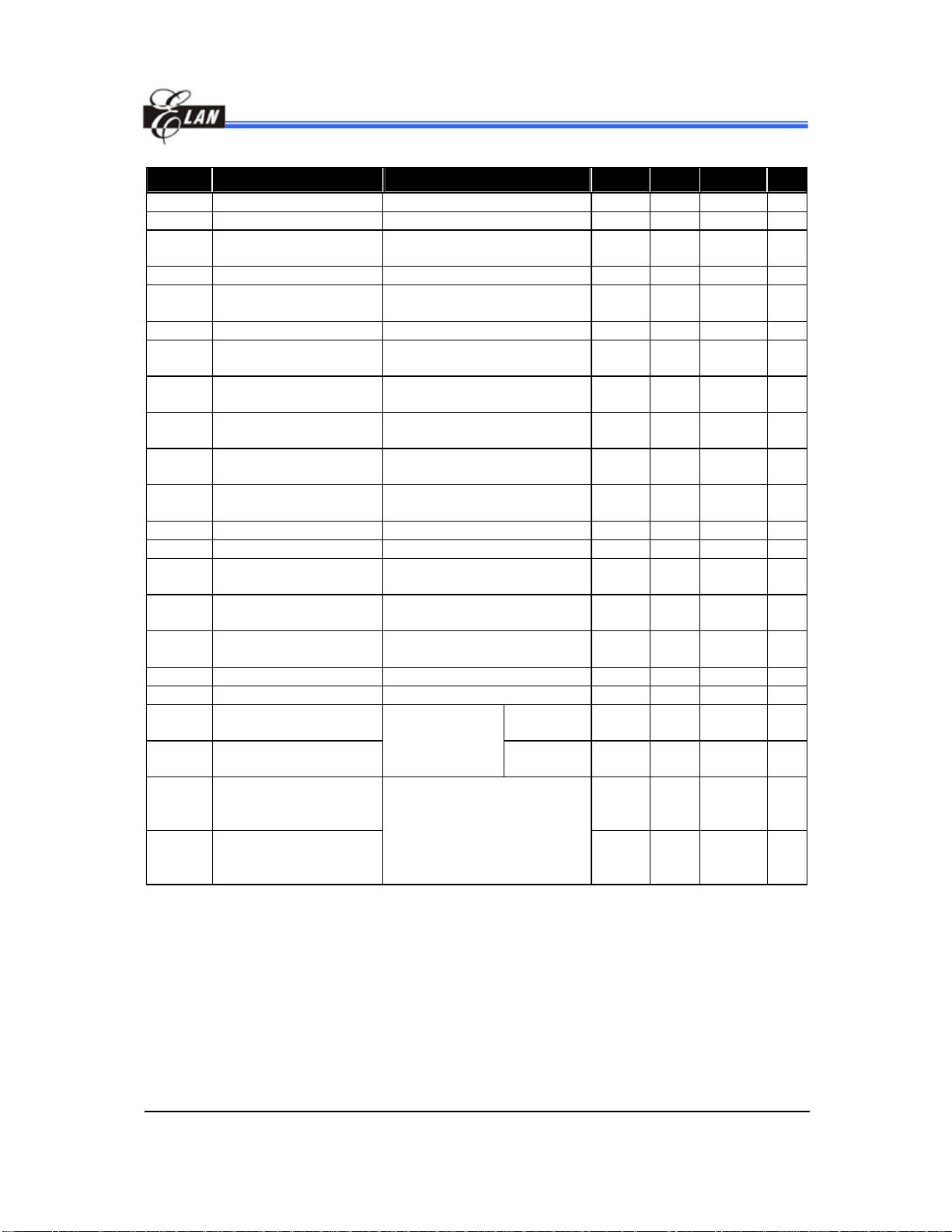
EM78P809N
8-Bit Microcontroller
(Ta= 25 °C, VDD= 3.0V ± 5%, VSS= 0V)
Symbol Parameter Condition Min. Typ. Max. Unit
Fc XTAL: 2.5V to VDD Two cyclea with two clocks 1 4 MHz
ERC ERC: VDD = 3V R: 5.1KΩ, C: 100 pF 600 850 1100 kHz
VIHRC
IRC1 Sink current VI from low to high , VI=5V 7 9.5 12 uA
VILRC
IRC2 Sink current VI from high to low , VI=2V 6 8.5 11 uA
IIL
VIH1
VIL1
VIHT2
VILT2
VIHX1 Clock Input High Voltage LOSCI,OSCI in crystal mode 0.7 VDD VDD +0.3V V
VILX1 Clock Input Low Voltage LOSCI,OSCI in crystal mode -0.3V 0.3 VDD V
IOH1
IOL1
IOL2
IPH Pull-high current Pull-high active, input pin at VSS -15 -23 -31 uA
IPL Pull-low current Pull-low active, input pin at VDD 15 23 30 uA
ISB1
ISB2
ICC3
ICC4
Input High Threshold
Voltage (Schmitt trigger)
Input Low Threshold
Voltage (Schmitt trigger)
Input Leakage Current for
input pins
Input High Voltage
(Schmitt trigger)
Input Low Voltage
(Schmitt trigger)
Input High Threshold
Voltage (Schmitt trigger)
Input Low Threshold
Voltage (Schmitt trigger)
Output High Voltage
(Ports 6, 7, 8, 9)
Output Low Voltage
(Ports9)
Output Low Voltage
(Ports 6,Port7, Port8)
Sleep mode
Power down current
Sleep mode
Power down current
Idle mode
Operating supply current
at two clocks
Normal mode
Operating supply current at
two clocks
OSCI in RC mode 1.6 2.3 2.8 V
OSCI in RC mode 0.7 1 1.3 V
VIN = VDD, VSS -1 0 1 μA
Ports 6,7,8,9,A 0.7VDD VDD+0.3V V
Ports 6,7,8,9,A -0.3V 0.3VDD V
/RESET, TCC 0.7 VDD VDD +0.3V V
/RESET, TCC -0.3V 0.3 VDD V
VOH = VDD-0.4V -2 -3.5 -5 mA
VOL = VSS+0.4V 2 3.5 5 mA
VOL = VSS+0.4V 10 13 16 mA
All input and I/O
pins at VDD,
output pin floating
VDD=3V, /RESET= 'High',
Fc=4MHz, CLKS="0", output pin
floating, WDT enabled
WDT disabled 0.4 0.8 μA
WDT enabled 1.5 3 μA
0.3 0.5 mA
1.1 1.5 mA
*The typical value is based on characterization results at 25°C
Product Specification
(This specification is subject to change without further notice)
(V1.0) 07 . 26.20 05 • 65
Page 70

EM78P809N
8-Bit Microcontroller
A/D Converter Characteristic (VDD =2.5V to 5.5V, Vss=0V, Ta = -40 to 85℃)
Symbol Parameter Condition Min. Typ. Max. Unit
VAREF 2.5 VDD V
VASS
VAI Analog input voltage VASS VAREF V
IAI1
IAI2
RN Resolution VDD =VAREF=5.0V, VASS =0.0V 9 10 Bits
LN Linearity error VDD = 2.5 to 5.5V Ta=25℃ 0 ±1 ±2 LSB
DNL
FSE Full scale error VDD =VAREF=5.0V, VASS =0.0V ±0 ±1 ±2 LSB
OE Offset error VDD =VAREF=5.0V, VASS =0.0V ±0 ±0.5 ±1 LSB
ZAI
TAD A/D clock period VDD =VAREF=5.0V, VASS =0.0V 4 us
TCN A/D conversion time VDD =VAREF=5.0V, VASS =0.0V 14 14 TAD
ADIV A/D input voltage range VDD =VAREF=5.0V, VASS =0.0V 0 VAREF V
ADOV A/D output voltage swing
PSR Power Supply Rejection VDD =5.0V±0.5V ±0 ±2 LSB
Analog reference voltage VAREF - VASS
IVDD 750 850 1000 uA
Analog supply current
Ivref
IVDD 500 600 820 uA
Analog supply current
IVref
Differential nonlinear
error
Recommended
impedance of analog
voltage source
≧2.5V
Vss Vss V
DD =VAREF=5.0V, VASS =0.0V
V
(V reference from V
DD =VAREF=5.0V, VASS =0.0V
V
(V reference from VREF)
DD = 2.5 to 5.5V Ta=25℃ 0 ±0.5 ±0.9 LSB
V
DD)
-10 0 +10 uA
200 250 300 uA
0 8 10 K
DD =VAREF=5.0V, VASS =0.0V,
V
RL=10K
0 0.2 0.3
4.7 4.8 5
V
• Product Specification (V1.0) 07.26.2005
66
(This specification is subject to change without further notice)
Page 71

EM78P809N
8-Bit Microcontroller
6.2 AC Electrical Characteristic
(Ta=- 40°C ~ 85 °C, VDD=5V ± 5%, VSS=0V)
Symbol Parameter Conditions Min Typ Max Unit
Dclk Input CLK duty cycle 45 50 55 %
Tins
Ttcc TCC input period
Tdrh
Trst /RESET pulse width Ta = 25°C 2000 ns
Twdt
Tset Input pin setup time 0 ns
Thold Input pin hold time 20 ns
Tdelay Output pin delay time Cload=20pF 50 ns
Tstup1 SDI data setup time Setup time of SDI data input to SCK↑or SCK↓ - 25 50 ns
Thold1 SDI data hold time Hold time of SDI data input to SCK↓or SCK↑ - 25 50 ns
Tvalid1 SDO output valid time SCK↑or SCK↓to SDO data output - 25 50 ns
Tsckh SCK input high time Slave mode (Fmain=8 MHz) 200 - - ns
Tsckl SCK input low time Slave mode (Fmain=8 MHz) 200 - - ns
Tsetup2 Slave mode setup
Tdelay1 Slave mode unselect
Instruction cycle time
(CLKS="0")
Device reset hold
time
Watchdog timer
period
time
delay time
Crystal type (high frequency) 200 DC ns
RC type 500 DC ns
(Tins+20)/
N*
Ta = 25°C 11.3 16.2 21.6 ms
°C 11.3 16.2 21.6 ms
Ta = 25
↓ to SCK↑or SCK↓(Fmain=8 MHz)
/SS
↑ to SDO output hi-impedance delay time
/SS
400 - - ns
- 25 50 ns
ns
* N= selected prescaler ratio
Product Specification
(This specification is subject to change without further notice)
(V1.0) 07 . 26.20 05 • 67
Page 72

EM78P809N
8-Bit Microcontroller
6.3 Timing Diagram
AC Test Input/Output Waveform
2.4
0.4
AC Testing : Input is driven at 2.4V for logic "1",and 0.4V for logic "0".Timing measurements are
made at 2.0V for logic "1",and 0.8V for logic "0".
2.0
0.8
TEST POINTS
2.0
0.8
RESET Timing (CLK="0")
NOP
CLK
/RESET
Tdrh
Instruction 1
Executed
TCC Input Timing (CLKS="0")
Tins
CLK
TCC
Ttcc
• Product Specification (V1.0) 07.26.2005
68
(This specification is subject to change without further notice)
Page 73

APPENDIX
Package Types:
EM78P809N
8-Bit Microcontroller
OTP MCU Package Type Pin Count Package Size
EM78P809NP DIP 28 600 mil
EM78P809NM SOP 28 300 mil
EM78P809NS SSOP 28 209 mil
Product Specification
(This specification is subject to change without further notice)
(V1.0) 07 . 26.20 05 • 69
Page 74

EM78P809N
8-Bit Microcontroller
CONTENTS.............................................................................................................III
1 General Description ··············· ·· ······················ ········································· ··········· 1
2 Features ·············································································································· 1
2.1 CPU ········································································································································ 1
2.2 Applications ···························································································································· 2
3 Pin Assignment ········ ······················ ··· ····················· ······················ ······················ 3
4 Pin Description ··································································································· 3
4 Function Description·························································································· 5
4.1 Functional Block Diagram ······································································································ 5
4.2 Operating Registers ··············································································································· 6
4.3 Special Purpose Registers··································································································· 23
4.4 CPU Operation Mode ··········································································································· 27
4.5 AD Converter························································································································ 29
4.6 Time Base Timer and Keytone Generator············································································ 31
4.7 UART (Universal Asynchronous Receiver/Transmitter)······················································· 33
4.8 SPI (Serial Peripheral Interface) ·························································································· 36
4.9 Timer/Counter 2 ··················································································································· 40
4.10 Timer/Counter 3 ··················································································································· 42
4.11 Timer/Counter 4 ··················································································································· 44
4.12 TCC/WDT & Prescaler ········································································································· 46
4.13 I/O Ports ······························································································································· 47
4.14 RESET and Wake-up ··········································································································· 47
4.15 Interrupt································································································································ 54
4.16 Oscillator ······························································································································ 55
4.17 Code Option Register··········································································································· 58
4.18 Power-on Considerations····································································································· 59
4.19 Instruction Set ······················································································································ 61
5 Absolute Maximum Ratings ·········· ··· ····················· ········································· · 63
5.1 Absolute Maximum Ratings ································································································· 63
5.2 Recommended Operating Conditions·················································································· 63
6 Electrical Characteristics··············· ··· ·· ··· ······················ ······················ ·············· 64
6.1 DC Electrical Characteristics································································································ 64
6.2 AC Electrical Characteristic·································································································· 67
6.3 Timing Diagram ··················································································································· 68
• Product Specification (V1.0) 07.26.2005
70
(This specification is subject to change without further notice)
Page 75

EM78P809N
8-Bit Microcontroller
APPENDIX ·············································································································· 69
Package Types:······························································································································ 69
Product Specification
(This specification is subject to change without further notice)
(V1.0) 07 . 26.20 05 • 71
 Loading...