

Page 1

EM78P221/2N
8-Bit Microcontroller
with OTP ROM
Product
Specification
DOC. VERSION 1.0
ELAN
MICROELECTRONICS CORP.
October 2007
Page 2

T rademark Acknowledgments:
IBM is a registered trademark and PS/2 is a trademark of IBM.
Windows is a trademark of Microsoft Corporation.
ELAN and ELAN logo are trademarks of ELAN Microelectronics Corporation.
Copyright © 2007 by ELAN Microelectronics Corporation
All Rights Reserved
Printed in Taiwan
The contents of this specification are subject to change without further notice. ELAN Microelectronics assume s no
responsibility concerning the accuracy , adequacy, or completeness of this specification. ELAN Microelectronics
makes no commitment to update, or to keep current the information and material contained in this specification.
Such information and material may change to conform to each confirm ed order.
In no event shall ELAN Microelectronics be made responsible for any claims attributed to errors, omissions, or
other inaccuracies in the informat ion or material contai ned in this specifi cation. ELAN Mi croelectronics shall n ot
be liable for direct, indirect, special incidental, or cons equenti al dama ges arising f rom the us e of such i nformat ion
or material.
The software (if any) described in this specification is furnished under a license or nondisclosure agreement, and
may be used or copied only in accordance with the terms of such agreement.
ELAN Microelectronics products are not intended for use in life support appliances, devices, or systems. Use of
ELAN Microelectronics product in such applications is not supported and is prohib ited.
NO PART OF THIS SPECIFICATION MAY BE REPRODUCED OR TRANSMITTED IN ANY FORM OR BY
ANY MEANS WITHOUT THE EXPRESSED WRITTEN PERMISSION OF ELAN MICROELECTRONICS.
ELAN MICROELECTRONICS CORPORATION
Headquarters:
No. 12, Innovation Road 1
Hsinchu Science Park
Hsinchu, TAIWAN 308
Tel: +886 3 563-9977
Fax: +886 3 563-9966
http://www.emc.com.tw
Hong Kong:
Elan (HK) Microelectronics
Corporation, Ltd.
Flat A, 19F., World Tech Centre 95
How Ming Street, Kwun Tong
Kowloon, HONG KONG
Tel: +852 2723-3376
Fax: +852 2723-7780
elanhk@emc.com.hk
Shenzhen:
Elan Microelectronics
Shenzhen, Ltd.
3F, SSMEC Bldg., Gaoxin S. Ave. I
Shenzhen Hi-tech Industrial Park
(South Area), Shenzhen
CHINA 518057
Tel: +86 755 2601-0565
Fax: +86 755 2601-0500
USA:
Elan Information
Technology Group (U.S.A.)
P.O. Box 601
Cupertino, CA 95015
U.S.A.
Tel: +1 408 366-8225
Fax: +1 408 366-8225
Shanghai:
Elan Microelectronics
Shanghai, Ltd.
#23, Zone 115, Lane 572, Bibo Rd.
Zhangjiang Hi-Tech Park
Shanghai, CHINA 201203
Tel: +86 21 5080-3866
Fax: +86 21 5080-4600
Page 3

Contents
Contents
EM78P221/2N-V Package version.................................................................................... 1
EM78P221/2N-U Package version ................................................................................... 1
1 General Description.................................................................................................. 2
2 Features ..................................................................................................................... 2
3 Pin Assignment......................................................................................................... 3
4 Pin Description.......................................................................................................... 4
4.1 EM78P222N ....................................................................................................... 4
4.2 EM78P221N ....................................................................................................... 5
5 Block Diagram........................................................................................................... 6
6 Function Description ................................................................................................ 7
6.1 Register Configuration........................................................................................ 7
6.2 Registers Description ......................................................................................... 8
6.2.1 A (Accumulator)...................................................................................................8
6.2.2 CONT (Control Register).....................................................................................8
6.2.3 R0 (Indirect Addressing Register) ......................................................................9
6.2.4 R1 (Memory Switch Register) .............................................................................9
6.2.5 R2 (Program Counter and Stack)........................................................................9
6.2.6 R3 (Status Register)..........................................................................................10
6.2.7 R4 (Select Indirect Address) ............................................................................. 11
6.2.8 Bank 0-R5 (Port 5) ............................................................................................11
6.2.9 Bank 0-R6 (Port 6) ............................................................................................11
6.2.10 Bank 0-R7 (Port 7) ............................................................................................11
6.2.11 Bank 0-R8 (Port 8) ............................................................................................11
6.2.12 Bank 0-R9~RD (Reserve) .................................................................................11
6.2.13 Bank 0-RE (WUCR: Wake-up Control Register)...............................................12
6.2.14 Bank 0-RF (Interrupt Status Register)...............................................................12
6.2.15 Bank 1-R5 ~R7 (I/O Port Control Register).......................................................13
6.2.16 Bank 1-R8 (I/O Port Control Register) ..............................................................13
6.2.17 Bank 1-R9 (Reserve).........................................................................................14
6.2.18 Bank 1-RA (CMPCON: Comparator Control Register) .....................................14
6.2.19 Bank 1-RB (Pull-down Control Register)...........................................................15
6.2.20 Bank 1-RC (Open-Drain Control Register) .......................................................15
6.2.21 Bank 1-RD (Pull-high Control Register) ............................................................16
6.2.22 Bank 1-RE (WDT Control Register) ..................................................................16
6.2.23 Bank 1-RF (Interrupt Mask Register) ................................................................17
6.2.24 Bank 2-R5 (HDCR: High Drive Control Register for Port 6)..............................18
6.2.25 Bank 2-R6 (HSCR1: High Sink Control Register for Port 5) .............................18
6.2.26 Bank 2-R7 (HSCR2: High Sink Control Register for Port 6) .............................19
Product Specification (V1.0) 10.19.2007 • iii
(This specification is subject to change without further notice)
Page 4

Contents
6.2.27 Bank 2-R8 (Operating Mode Control Register).................................................19
6.2.28 Bank 2-R9~RF (Reserve)..................................................................................19
6.2.29 Bank 3-R5 (Timer Clock/Counter).....................................................................19
6.2.30 Bank 3-R6 (IRC Control)-only for ICE ...............................................................20
6.2.31 Bank 3-R7 (Noise and LVR Control) - only for ICE ...........................................21
6.2.32 Bank 3-R8~RF (Reserve)..................................................................................21
6.2.33 R10 ~ R1F .........................................................................................................21
6.2.34 Banks 0~3 - R20 ~ R3F ....................................................................................21
6.3 TCC/WDT and Prescaler.................................................................................. 22
6.4 I/O Ports ........................................................................................................... 23
6.4.1 Usage of Port 6 Input Change Wake-up/Interrupt Function..............................25
6.5 Reset and Wake-up.......................................................................................... 26
6.5.1 Reset and Wake-up Operation..........................................................................26
6.5.1.1 Wake-up and Interrupt Modes Operation Summary ..........................28
6.5.1.2 Register Initial Values after Reset ......................................................30
6.5.1.3 Controller Reset Block Diagram........................................................34
6.5.2 The T and P Status under Status Register........................................................35
6.6 Interrupt ............................................................................................................ 36
6.7 Comparator ...................................................................................................... 38
6.7.1 External Reference Signal ................................................................................38
6.7.2 Comparator Outputs..........................................................................................38
6.7.3 Using a Comparator as an Operation Amplifier.................................................39
6.7.3.1 Bank 0-RE (WUCR: Wake-up Control Register)................................39
6.7.3.2 Bank 1-RA (CMPCON: Comparator Control Register) ......................40
6.7.3.3 Bank 1-RE (WDT Control Register) ...................................................40
6.7.4 Comparator Interrupt.........................................................................................40
6.7.5 Wake-up from Sleep Mode................................................................................40
6.8 Oscillator .......................................................................................................... 41
6.8.1 Oscillator Modes................................................................................................41
6.8.2 Crystal Oscillator/Ceramic Resonators (Crystal)...............................................41
6.8.3 External RC Oscillator Mode.............................................................................44
6.8.4 Internal RC Oscillator Mode ..............................................................................45
6.9 Power-on Considerations ................................................................................. 45
6.9.1 External Power-on Reset Circuit .......................................................................45
6.9.2 Residual Voltage Protection ..............................................................................46
6.10 Low Voltage Reset ........................................................................................... 46
6.11 Code Option ..................................................................................................... 47
6.11.1 Code Option Register (Word 0).........................................................................47
6.11.2 Code Option Register (Word 1).........................................................................49
6.11.3 Customer ID Register (Word 2).........................................................................50
6.12 Instruction Set .................................................................................................. 50
iv •
Product Specification (V1.0) 10.19.2007
(This specification is subject to change without further notice)
Page 5

Contents
7 Absolute Maximum Ratings................................................................................... 53
8 DC Electrical Characteristics................................................................................. 53
8.1 Comparator (OP) Characteristic....................................................................... 55
9 AC Electrical Characteristic................................................................................... 55
10 Timing Diagrams..................................................................................................... 56
APPENDIX
A Package Type........................................................................................................... 57
B Packaging Configuration........................................................................................ 58
B.1 24-Lead Plastic Skinny Dual in line (SDIP) — 300 mil ..................................... 58
B.2 24-Lead Plastic Small Outline (SOP) — 300 mil .............................................. 59
B.3 24-Lead Plastic Shrink Small Outline (SSOP) — 209 mil ................................ 60
B.4 28- Lead Plastic Skinny Dual in line (SDIP) — 300 mil .................................... 61
B.5 28-Lead Plastic Small Outline (SOP) — 300 mil .............................................. 62
B.6 28- Lead Plastic Shrink Small Outline (SSOP) — 209 mil ............................... 63
C Quality Assurance and Reliability ........................................................................ 64
C.1 Address Trap Detect......................................................................................... 64
Product Specification (V1.0) 10.19.2007 • v
(This specification is subject to change without further notice)
Page 6

Contents
Specification Revision History
Doc. Version Revision Description Date
0.9 Preliminary version 2007/03/20
1.0 Initial released version 2007/10/19
vi •
Product Specification (V1.0) 10.19.2007
(This specification is subject to change without further notice)
Page 7

EM78P221/2N
8-Bit Microcontroller with OTP ROM
Read Me First !
Comparison between V-Package and U-Package version
This series of microcontrollers comprise of the older V-package version and the newer
U-package version. In the newer U-package version, a Code Option NRM is added
and various features such as Crystal mode Operating frequency range, IRC mode
wake-up time, WDT Time-out time, Comparator function and Pins function have been
modified to favorably meet users’ requirements. The following table is provided for
quick comparison between the two package version and for user convenience in the
choice of the most suitable product for their application.
EM78P221/222N-V EM78P221/222N-U
Crystal mode Operating
frequency range at 0°C~ 70°C
IRC mode wake-up time
Sleep mode → Normal mode
Condition: 5V, 4MHz
P52, P53 Function Output only Input / Output
Comparator Function Comparator only Comparator / OPA
WDT Time-out time
(Prescaler = 1 : 1)
Condition: VDD = 5V
Code Option
DC ~ 12MHz, 4.0V
DC ~ 8MHz, 3.0V
DC ~ 4MHz, 2.1V
64μs 10μs
16.5 ms ± 30 % 15.2 ms ± 30 %
×
DC ~ 16MHz, 4.5V
DC ~ 8MHz, 3.0V
DC ~ 4MHz, 2.1V
Added a Code Option NRM
EM78P221/2N-V Package version EM78P221/2N-U Package version
Product Specification (V1.0) 10.19.2007 • 1
(This specification is subject to change without further notice)
Page 8

EM78P221/2N
8-Bit Microcontroller with OTP ROM
1 General Description
EM78P221N and EM78P222N are 8-bit microprocessors designed and developed with low-power and high-speed CMOS
technology. Each device in the series has as an on-chip 4K×13-bit Electrical One Time Programmable Read Only Memory
(OTP-ROM). Each provides a protection bit to prevent intrusion of user’s OTP memory code. Two Code option bits are
also available to meet user’s requirements.
With its enhanced OTP-ROM features, each device provides a convenient way of developing and verifying user’s
programs. Moreover, this OTP devices offer the advantages of easy and effective program updates, using development
and programming tools. User can avail of the ELAN Writer to easily program his development code.
2 Features
CPU configuration
• 4K×13 bits on-chip OTP-ROM
• 144×8 bits on-chip registers (SRAM)
• 8-level stacks for subroutine nesting
• 3 programmable Level Voltage Reset
(LVR) : 4.0V, 3.0V, 2.5V
• Less than 1.5 mA at 5V/4MHz
• Typically 15 μA, at 3V/32kHz
• Typically 2 μA, during sleep mode
I/O port configuration
• 4 bidirectional I/O ports: P5, P6, P7 and P8
• Wake-up port : P6
• 26 I/O pins
• 8 programmable pull-down I/O pins
• 8 programmable pull-high I/O pins
• 8 programmable open-drain I/O pins
• 16 Programmable high sink current I/O pins
• 8 Programmable high drive current I/O pins
• External interrupt : P77, P71
Operating voltage range:
• OTP version:
Operating voltage range: 2.1V~5.5V (commercial)
Operating voltage range: 2.3V~5.5V (industrial)
Operating temperature range:
Operating temperature range: 0°C~70°C
(commercial)
Operating temperature range: -40°C~85°C
(industrial)
Operating frequency range
• Crystal mode:
DC~16MHz/2 clks @ 4.5V; DC~125ns inst. cycle
@ 4.5V
DC ~ 8MHz/2 clks @ 3V; DC~250ns inst. Cycle
@ 3V
• ERC mode:
DC ~ 16MHz/2 clks @ 4.5V; DC~125ns inst.
cycle @ 5V
DC ~ 8MHz/2 clks @ 3V; DC ~ 250ns inst. Cycle
@ 3V
• IRC mode:
Oscillation mode: 16MHz, 4 MHz, 1 MHz, 455kHz
Process deviation: Typ ± 3%, Max. ± 5%
Temperature deviation: ± 5% (-40°C~85°C)
Product Specification (V1.0) 10.19.2007
2 •
(This specification is subject to change without further notice)
Internal RC
Frequency
4MHz ±5% ±5% ±4% ±14%
16MHz ±5% ±5% ±4% ±14%
1MHz ±5% ±5% ±4% ±14%
455kHz ±5% ±5% ±4% ±14%
All these four main frequencies can be trimmed by
programming with four calibrated bits in the ICE220N
Simulator. OTP is auto trimmed by ELAN Writer
(DWTR).
Fast set-up time requires only 800μs (VDD:5V,
Crystal: 4MHz, C1/C2: 30pF) in HXT2 mode and 10μs in
IRC mode (VDD:5V IRC:4MHz)
Peripheral configuration
• 8-bit real time clock/counter (TCC) with selective
signal sources, trigger edges, and overflow interrupt
• One comparator (can act as an OP).
(offset voltage is smaller than 10mV)
Five available interrupts
• TCC overflow interrupt
• Input-port status changed interrupt (wake up from
sleep mode)
• Two External interrupts
• Comparator high/low interrupt
Special Features
• Programmable free running Watchdog Timer
• Two clocks per instruction cycle
• Power-on voltage detector available (1.8 V± 0.1V)
• High EFT immunity (better performance at 4MHz or
below
• Power saving Sleep mode
• Selectable Oscillation mode
• Package Type:
• 24-pin skinny DIP 300mil : EM78P221NKJ/NKS
• 24 pin SOP 300mil : EM78P221NMJ/NMS
• 24 pin SSOP 209mil : EM78P221NAMJ/NAMS
• 28-pin skinny DIP 300mil : EM78P222NKJ/NKS
• 28 pin SOP 300mil : EM78P222NMJ/NMS
• 28 pin SSOP 209mil : EM78P222NAMJ/NAMS
Temperature
(-40°C+85°C)
Drift Rate
Voltage
(2.1V~5.5V)
Process Total
Page 9

3 Pin Assignment
(1) 28-Pin DIP/SOP/SSOP
8-Bit Microcontroller with OTP ROM
(2) 24-Pin DIP/SOP/SSOP
EM78P221/2N
1
P55
P56/TCC
P77/INT0
VSS
P60
P61
P62
P63
P64
P50
P51
P80
P76
2
3
4
5
EM78P222N
6
7
8
9
10
11
12
13
14
Fig. 3-1 EM78P222NK/AK/M/AM
28
27
26
25
24
23
22
21
20
19
18
17
16
15
P81//RESET
P53/OSCI
P52/OSCOVDD
P70
P71/CO/INT1
P72/CIN+
P73/CIN-
P67
P66
P65
P57
P54
P74
P75
1
P55
VSS
P60
P61
P62
P63
P64
P50
P51
2
3
4
EM78P221N
5
6
7
8
9
10
11
12
P56/TCC
P77/INT0
24
23
22
21
20
19
18
17
16
15
14
13
P81//RESET
P53/OSCI
P52/OSCOVDD
P70
P71/CO/INT1
P72/CIN+
P73/CINP67
P66
P65
P57
P54
Fig. 3-2 EM78P221NK/M/AM
Product Specification (V1.0) 10.19.2007 • 3
(This specification is subject to change without further notice)
Page 10

EM78P221/2N
8-Bit Microcontroller with OTP ROM
4 Pin Description
4.1 EM78P222N
Symbol Pin No. Type Function
1~2
P50~P57
P60~P67
P70~ P77
P80, P81
CINCIN+
CO
OSCI
OSCO
/RESET
INT0~INT1
VDD
VSS
11~12
17~18
26~27
6 ~ 10
19 ~21
5
14 ~ 16
22~25
13, 28 I/O
22
23
24
27 I
26 O
28 I
5, 24 I
3 -
4 -
I/O
I/O
I/O
O
8-bit General purpose input/output pins
Default value at power-on reset
8-bit General purpose input/output pins
Default value at power-on reset
8-bit General purpose input/output pins
Default value at power-on reset.
P72 and P73 are open drain pins when used as output pins in
ICE220N simulator.
2-bit General purpose input or output pin
Default value at power-on reset
P81 is define as General purpose input or output open-drain
pin.
“-“ : input pin of Vin- of the comparator
I
“+” : input pin of Vin+ of the comparator
I
Pin CO is the comparator output
Defined by CMPCON (Bank 1-RA) <3 : 4>
Crystal type: Crystal input terminal
RC type: RC oscillator input pin
Crystal type: Output terminal for crystal oscillator.
RC type: Clock output with a duration of one instruction cycle
time.
External clock signal input.
If it remains at a logic low, the device will be reset
Wake-up from sleep mode when pin status changes
Voltage on /RESET must not exceed Vdd during normal mode
External interrupt pin
Power supply
Ground
Product Specification (V1.0) 10.19.2007
4 •
(This specification is subject to change without further notice)
Page 11

4.2 EM78P221N
Symbol Pin No. Type Function
P50~P57
P60~P67
P70~P73
P77
P81
CINCIN+
CO
OSCI
OSCO
/RESET
INT0~INT1
VDD
VSS
1~2
11~14
22~23
6 ~ 10
15~17
5
21 ~ 18
24 I/O
18
19
20
23 I
22 O
24 I
5, 20 I
3 -
4 -
I/O
I/O
I/O
I
I
O
EM78P221/2N
8-Bit Microcontroller with OTP ROM
8-bit General purpose input/output pins
Default value at power-on reset.
8-bit General purpose input/output pins
Default value at power-on reset
5-bit General purpose input/output pins
Default value at power-on reset
P72 and P73 are open drain pins when used as output pins of
the ICE220N simulator.
1-bit General purpose input or output open-drain pin
Default value at power-on reset
“-“ : input pin of Vin- of the comparator
“+” : input pin of Vin+ of the comparator
Pin CO is the comparator output
Defined by CMPCON (Bank 1-RA) <3 : 4>
Crystal type: Crystal input terminal
RC type: RC oscillator input pin
Crystal type: Output terminal for crystal oscillator
RC type: Clock output with a duration of one instruction cycle
time.
External clock signal input.
If it remains at logic low, the device will be reset
Wake-up from sleep mode when pin status changes
Voltage on /RESET must not exceed Vdd during normal mode
External interrupt pin
Power supply
Ground
Product Specification (V1.0) 10.19.2007 • 5
(This specification is subject to change without further notice)
Page 12
EM78P221/2N
8-Bit Microcontroller with OTP ROM
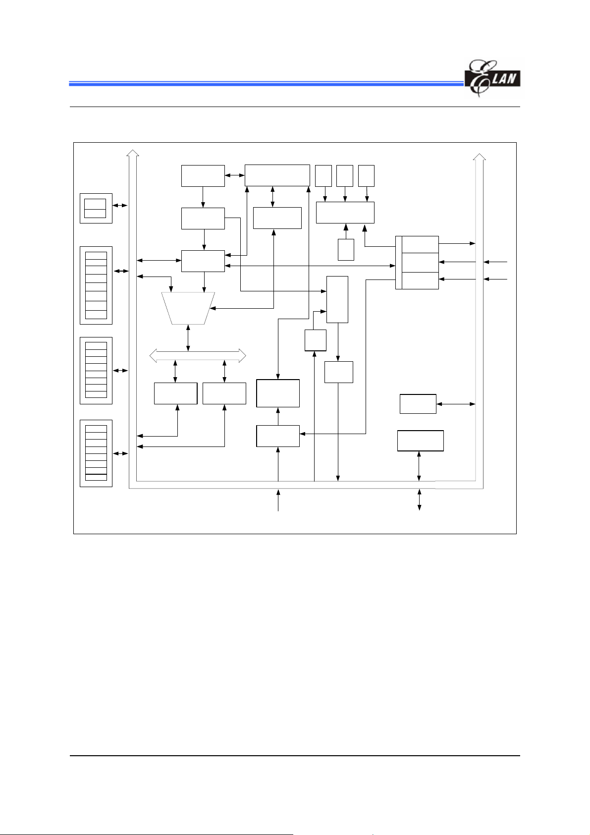
5 Block Diagram
P8
P80
P81
P70
P71
P72
P73
P74
P75
P76
P77
P60
P61
P62
P63
P64
P65
P66
P67
P50
P51
P52
P53
P54
P55
P56
P57
P7
P6
P5
ACC
ROM
Instruction
Register
Instruction
Decoder
ALU
R3 (Status
Reg.)
PC
8-level stack
(13 bit)
Interrupt
Control
Register
Interrupt
Circuit
R4
Ext.
OSC.
Int.
RC
Oscillation
Generation
Reset
Mux
.
RAM
Ext.
RC
WDT
TCC
Port
change
LVR
Comparator
TCC
Port 6
Ext INT
Cin+ Cin- CO
Fig. 5-1 EM78P221/2N Functional Block Diagram
6 •
(This specification is subject to change without further notice)
Product Specification (V1.0) 10.19.2007
Page 13

EM78P221/2N
8-Bit Microcontroller with OTP ROM
6 Function Description
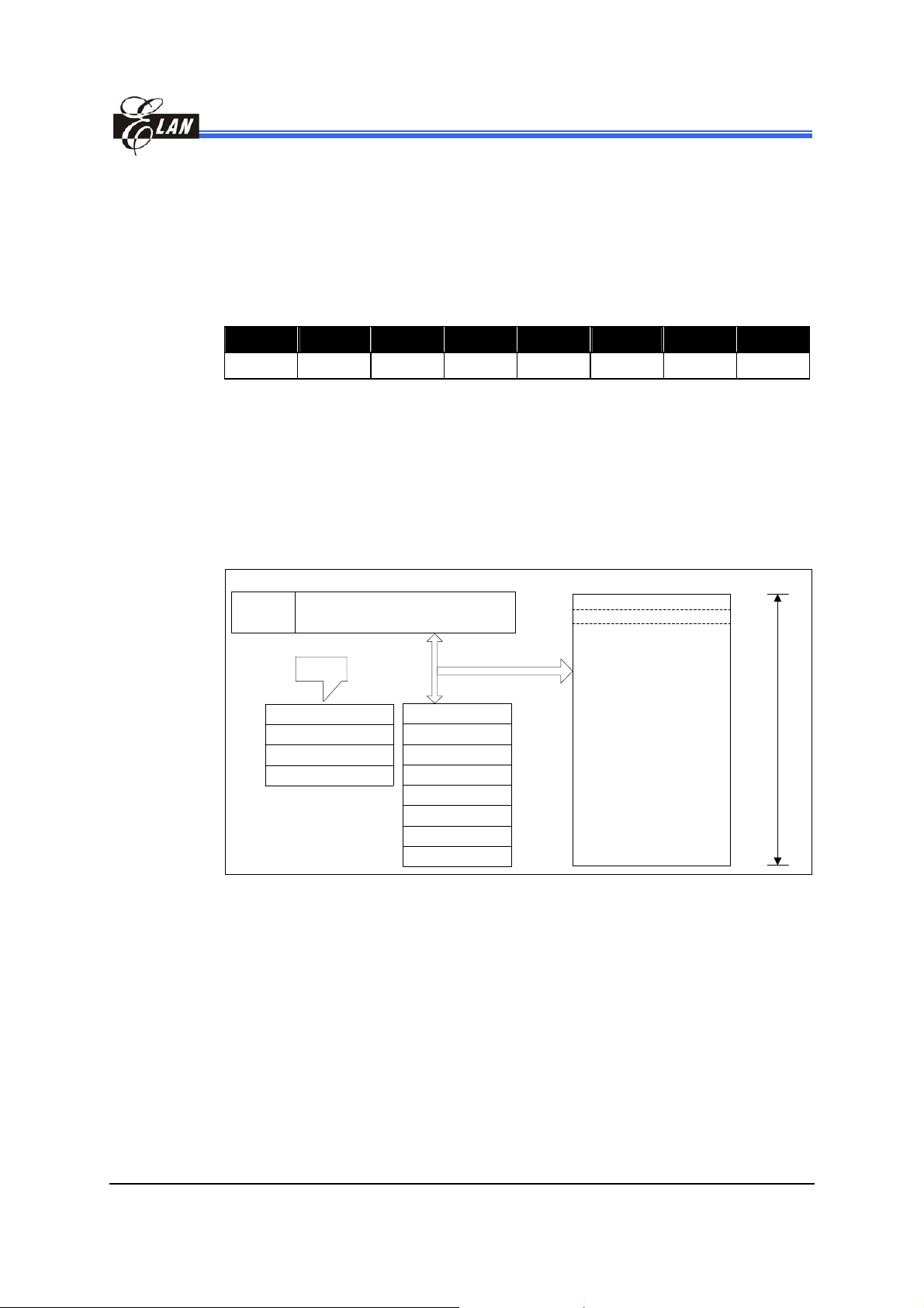
6.1 Register Configuration
Address Bank 0 Registers Bank 1 Registers Bank 2 Registers Bank 3 Registers
00 R0 (Indirect Addressing Register)
01 R1 (Memory switch register)
02 R2 (Program Counter)
03 R3 (Status Register)
04 R4 (Select Indirect Address)
05 R5 (Port 5)
06 R6 (Port 6)
07 R7 (Port 7)
08 R8 (Port 8)
09 Reserve Reserve Reserve Reserve
0A Reserve
0B Reserve
0C Reserve
0D Reserve
0E
0F
10
:
1F
20
:
3F
RE (Wake-up Control
Register)
RF (Interrupt Status
Register)
General Registers (16×8 bits)
General Registers
(32×8 bits)
R5 (I/O Port Control
Register)
R6 (I/O Port Control
Register)
R7 (I/O Port Control
Register)
R8 (I/O Port Control
Register)
RA (Comparator Control
Register)
RB (Pull-down Control
Register)
RC (Open-drain Control
Register)
RD (Pull-high Control
Register)
RE (WDT Control
Register)
RF (Interrupt Mask
Register)
General Registers
(32×8 bits)
R5 (High Drive Control
Register for Port 6)
R6 (High Sink Control
Register for Port 5)
R7 (High Sink Control
Register for Port 6
Reserve Reserve
Reserve Reserve
Reserve Reserve
Reserve Reserve
Reserve Reserve
Reserve Reserve
Reserve Reserve
General Registers
(32×8 bits)
R5 (Timer Clock /
Counter)
Reserve*
Reserve*
General Registers
(32×8 bits)
Note: 1. All registers are 8 bits.
2. When using ICE, some registers code options are set. Refer to Section 6.2 for detailed Registers Description.
3. Registers with * can only be used in ICE220N simulator.
Product Specification (V1.0) 10.19.2007 • 7
(This specification is subject to change without further notice)
Page 14

EM78P221/2N
8-Bit Microcontroller with OTP ROM
6.2 Registers Description
6.2.1 A (Accumulator)
Internal data transfer operation, or instruction operand holding usually involves the
temporary storage function of the Accumulator. The Accumulator is not an
addressable register.
6.2.2 CONT (Control Register)
Bit 7 Bit 6 Bit 5 Bit 4 Bit 3 Bit 2 Bit 1 Bit 0
INTE INT TS TE PSTE PST2 PST1 PST0
Bit 7 (INTE): INT signal edge
0 = interrupt occurs at the rising edge on the INT0 and INT1 pin
1 = interrupt occurs at the falling edge on the INT0 and INT1 pin
Bit 6 (INT): Interrupt enable flag
0 = masked by DISI or hardware interrupt
1 = enabled by the ENI/RETI instructions
This bit is readable only.
Bit 5 (TS): TCC signal source
0 = internal instruction cycle clock. If P56 is used as I/O pin, TS must be 0.
1 = transition on the TCC pin
Bit 4 (TE): TCC signal edge
0 = increment if the transition from low to high takes place on the TCC pin
1 = increment if the transition from high to low takes place on the TCC pin.
Bit 3 (PSTE): Prescaler enable bit for TCC
0 = prescaler disable bit. TCC rate is 1:1
1 = prescaler enable bit. TCC rate is set as Bit 2 ~ Bit 0.
Bit 2 ~ Bit 0 (PST2 ~ PST0): TCC prescaler bits
PST2 PST1 PST0 TCC Rate
0 0 0 1:2
0 0 1 1:4
0 1 0 1:8
0 1 1 1:16
1 0 0 1:32
1 0 1 1:64
1 1 0 1:128
1 1 1 1:256
Note: Tcc time-out period [1/Fosc x prescaler x (256 -Tcc cnt) x 1]
Fosc: Oscillator (Crystal, ERC, IRC) frequency
Product Specification (V1.0) 10.19.2007
8 •
(This specification is subject to change without further notice)
Page 15
EM78P221/2N
8-Bit Microcontroller with OTP ROM
6.2.3 R0 (Indirect Addressing Register)
R0 is not a physically implemented register. Its major function is to perform as an
indirect address pointer. Any instruction using R0 as a pointer, actually accesses the
data pointed by the RAM Select Register (R4).
6.2.4 R1 (Memory Switch Register)
Bit 7 Bit 6 Bit 5 Bit 4 Bit 3 Bit 2 Bit 1 Bit 0
“0” “0” “0” “0” “0” “0” BS1 BS0
Bits 7~2: not used bits, fixed to 0 all the time.
Bits 1~0: used to select Banks 0 ~ 3 for R20~R3F and select Banks 0 ~ 3 for the
control register.
See the table under Section 6.2 Registers Description for the data memory
configuration.
6.2.5 R2 (Program Counter and Stack)
A11 A10
R1(5,4)
00 PAGE0 0000~03FF
01 PAGE1 0400~07FF
10 PAGE2 0800~0BFF
11 PAGE3 0C00~0FFF
A9 ~ A0
CALL
RET
RETL
RETI
Stack Level 1
Stack Level 2
Stack Level 3
Stack Level 4
Stack Level 5
Stack Level 6
Stack Level 7
Stack Level 8
Fig. 6-1 Program Counter Organization
Reset Vector
Interrupt Vector
On-chip Program
Memory
R2 and hardware stacks are 12-bit wide. The structure is depicted in the table under
Section
6.1 Register Configuration.
Generates 4K×13 bits on-chip ROM addresses to the relative programming instruction
codes. One program page is 1024 words long.
000H
008H
User Memory Space
FFFH
The contents of R2 are all set to "0"s when a reset condition occurs.
Product Specification (V1.0) 10.19.2007 • 9
(This specification is subject to change without further notice)
Page 16

EM78P221/2N
8-Bit Microcontroller with OTP ROM
"JMP" instruction allows direct loading of the lower 10 program counter bits. Thus,
"JMP" allows PC to jump to any location within a Page (1K).
"CALL" instruction loads the lower 10 bits of the PC, and then PC+1 is pushed into the
stack. Thus, the subroutine entry address can be located anywhere within a page (1K).
"LJMP" instruction allows direct loading of the lower 11 program counter bits.
Therefore, "LJMP" allows PC to jump to any location within 2K (2
"LCALL" instruction loads the lower 11 bits of the PC, and then PC+1 are pushed onto
the stack. Thus, the subroutine entry address can be located anywhere within 2K (2
12
).
12
).
"RET" ("RETL k", "RETI") instruction loads the program counter with the contents of the
top of stack.
"ADD R2, A" allows a relative address to be added to the current PC, and the ninth and
above bits of the PC will increase progressively.
"MOV R2, A" allows loading of an address from the "A" register to the lower 8 bits of the
PC, and the ninth and above bits of the PC will remain unchanged.
Any instruction (except “ADD R2,A”) that is written to R2 (e.g., "MOV R2, A", "BC R2, 6"
etc.) will cause the ninth bit and above bits of the PC to remain unchanged.
All instructions are single instruction cycle (fclk/2) except “LCALL” and “LJMP”
instructions. The “LCALL” and “LJMP” instructions need two instructions cycle.
6.2.6 R3 (Status Register)
Bit 7 Bit 6 Bit 5 Bit 4 Bit 3 Bit 2 Bit 1 Bit 0
- - - T P Z DC C
Bits 7~5: not used, fixed to 0 all the time.
Bit 4 (T): Time-out bit. Set to 1 by the "SLEP" and "WDTC" commands or during
power on and reset to 0 by WDT time-out.
Bit 3 (P): Power-down bit. Set to 1 during power on or by a "WDTC" command
and reset to 0 by a "SLEP" command.
NOTE
Bit 4 & Bit 3 (T & P) are read only.
Bit 2 (Z): Zero flag. Set to "1" if the result of an arithmetic or logic operation is
zero.
Bit 1 (DC): Auxiliary carry flag
Bit 0 (C): Carry flag
Product Specification (V1.0) 10.19.2007
10 •
(This specification is subject to change without further notice)
Page 17

EM78P221/2N
8-Bit Microcontroller with OTP ROM
6.2.7 R4 (Select Indirect Address)
Bits 7~6: not used, fixed to 0 all the time.
Bit 5 ~ Bit 0: used to select registers (Address: 00 ~ 3F) in indirect addressing mode.
6.2.8 Bank 0-R5 (Port 5)
Bit 7 Bit 6 Bit 5 Bit 4 Bit 3 Bit 2 Bit 1 Bit 0
P57 P56 P55 P54 P53 P52 P51 P50
Bits 7 ~ 0 (P57 ~ P50): I/O data bits
6.2.9 Bank 0-R6 (Port 6)
Bit 7 Bit 6 Bit 5 Bit 4 Bit 3 Bit 2 Bit 1 Bit 0
P67 P66 P65 P64 P63 P62 P61 P60
Bits 7 ~ 0 (P67 ~ P60): I/O data bits
6.2.10 Bank 0-R7 (Port 7)
Bit 7 Bit 6 Bit 5 Bit 4 Bit 3 Bit 2 Bit 1 Bit 0
P77 P76 P75 P74 P73 P72 P71 P70
Bits 7 ~ 0 (P77 ~ P70): I/O data bits
[With Simulator]: P73 ~ P72 are input or open-drain output pins.
[With EM78P221/2N]: P73 ~ P72 are general input or output pins.
6.2.11 Bank 0-R8 (Port 8)
Bit 7 Bit 6 Bit 5 Bit 4 Bit 3 Bit 2 Bit 1 Bit 0
0 0 NREN 0 0 0 P81 P80
Bits 7~6, 4~2, 0: not used, fixed to 0 all the time.
Bit 5 (NREN): Noise rejection enable
0 = disable noise rejection (Default)
1 = enable noise rejection. However in crystal oscillator mode
(LXT2), the noise rejection circuit is always disabled.
Bits 1 ~0 (P81~P80): I/O data bit.
6.2.12 Bank 0-R9~RD (Reserve)
Bits 7~0: not used, fixed to "0" all the time.
Product Specification (V1.0) 10.19.2007 • 11
(This specification is subject to change without further notice)
Page 18

EM78P221/2N
8-Bit Microcontroller with OTP ROM
6.2.13 Bank 0-RE (WUCR: Wake-up Control Register)
Bit 7 Bit 6 Bit 5 Bit 4 Bit 3 Bit 2 Bit 1 Bit 0
EX1IF 0 0 ICWE 0 CMPWE 0 CMPIF
Bit 7 (EX1IF): External interrupt flag. Set by INT1 pin, reset by software.
0 = no interrupt occurs
1 = with interrupt request
Bits 6~5, 3, 1: not used bits, fixed to 0 all the time
Bit 4 (ICWE): Port 6 input change to wake-up status enable bit
0 = Disable Port 6 input change to wake-up status
1 = Enable Port 6 input change wake-up status
When the Port 6 Input Status Change is used to enter interrupt vector or
to wake-up EM78P221N//2N from sleep, the ICWE bit must be set to
“Enable“.
Bit 2 (CMPWE): Comparator wake-up enable bit
0 = Disable Comparator wake-up
1 = Enable Comparator wake-up
When the Comparator output status change is used to enter interrupt
vector or to wake-up from sleep, the CMPWE bit must be set to
“Enable“.
Bit 0 (CMPIF): Comparator interrupt flag. Set when a change occurs in the output of
Comparator. Reset by software.
0 = no interrupt occurs
1 = with interrupt request
NOTE
■ Bank 0-RE <7, 0> can be cleared by instruction but cannot be set.
■ Bank1-RE <0> is an interrupt mask register.
■ Interrupt results from "logic AND" of Bank 0-RE <7, 0> and Bank 1-RE <0>, with
instruction “ENI”.
6.2.14 Bank 0-RF (Interrupt Status Register)
Bit 7 Bit 6 Bit 5 Bit 4 Bit 3 Bit 2 Bit 1 Bit 0
0 0 0 0 0 EX0IF ICIF TCIF
Bits 7~3: not used bits, fixed to 0 all the time
Bit 2 (EX0IF): External interrupt flag. Set by INT0 pin. Reset by software.
0 = no interrupt occurs
1 = with interrupt request
Product Specification (V1.0) 10.19.2007
12 •
(This specification is subject to change without further notice)
Page 19

EM78P221/2N
8-Bit Microcontroller with OTP ROM
Bit 1 (ICIF): Port 6 input status change interrupt flag. Set when Port 6 input changes.
Reset by software.
0 = no interrupt occurs
1 = with interrupt request
Bit 0 (TCIF): TCC overflow interrupt flag. Set when TCC overflows. Reset by software.
0 = no interrupt occurs
1 = with interrupt request
NOTE
■ Bank 0-RF <2, 1, 0> can be cleared by instruction but cannot be set.
■ Bank1-RF <2, 1, 0> is an interrupt mask register.
■ Interrupt results from "logic AND" of Bank 0-RF <2, 1, 0> and Bank 1-RF <2, 1, 0>
with instruction “ENI”.
6.2.15 Bank 1-R5 ~R7 (I/O Port Control Register)
Bits 7~0: 0 = defines the relative I/O pin as output
1 = puts the relative I/O pin into high impedance
Bank 1-R5, R6 and R7 registers are all readable and writable.
6.2.16 Bank 1-R8 (I/O Port Control Register)
Bit 7 Bit 6 Bit 5 Bit 4 Bit 3 Bit 2 Bit 1 Bit 0
0 0 0 0 0 0 C81 C80
Bits 7~2: not used, fixed to 0 all the time
Bits 1~0 (C81~C80): 0 = defines the relative I/O pin as output
1 = puts the relative I/O pin into high impedance
With Simulator]: P80 and P81 are General I/O pins
[With EM78P221/2N]: P80 is General input or output, but P81 is input or open-drain
output pin.
Product Specification (V1.0) 10.19.2007 • 13
(This specification is subject to change without further notice)
Page 20

EM78P221/2N
8-Bit Microcontroller with OTP ROM
6.2.17 Bank 1-R9 (Reserve)
Bits 7~0: not used, fixed to 0 all the time
6.2.18 Bank 1-RA (CMPCON: Comparator Control Register)
Bit 7 Bit 6 Bit 5 Bit 4 Bit 3 Bit 2 Bit 1 Bit 0
EIS1 EIS0 CMPOUT CMPCOS1 CMPCOS0 0 0 0
Bit 7 (EIS1): Control bit used to define the function of the P71 (/INT1) pin
0 = P71, normal I/O pin
1 = /INT1, external interrupt pin. In this case, the I/O control bit of P71
(Bit 1 of Bank 1-R7) must be set to "1"
Bit 6 (EIS0): Control bit used to define the function of the P77 (/INT0) pin
0 = P77, normal I/O pin
1 = /INT0, external interrupt pin. In this case, the I/O control bit of P77
(Bit 7 of Bank 1-R7) must be set to "1"
NOTE
When EIS is "0," the path of /INT is masked. When EIS is "1," the status of /INT
pin can also be read by way of reading Port 7 (Bank 0-R7). Refer to Fig. 6-4 (I/O
Port and I/O Control Register Circuit for P77 (/INT0) and P71 (/INT1) under
Section 6.4 (I/O Ports).
EIS0 and EIS1 are both readable and writable.
The highest priority of P71/INT1/CO2 is INT1. When EIS1=0, the working type
of P71/INT1/CO is determined by CMPCOS1 and CMPCOS0.
Bit 5 (CMPOUT): The result of the comparator output
Bit 4 ~ Bit 3 (CMPCOS1 ~ CMPCOS0): Comparator Select bits
CMPCOS1 CMPCOS0 Function Description
0 0
0 1
1 0
1 1 Used as OP and P71 is OP output pin (CO)
Comparator is not used. P72, P73 and P71 are
normal I/O pins
P72 and P73 are Comparator input pins and P71
is normal I/O pin
P72 and P73 are Comparator input pins and P71
is Comparator output pin (CO)
Bits 2~0: not used, fixed to 0 all the time
Product Specification (V1.0) 10.19.2007
14 •
(This specification is subject to change without further notice)
Page 21

EM78P221/2N
8-Bit Microcontroller with OTP ROM
6.2.19 Bank 1-RB (Pull-down Control Register)
Bit 7 Bit 6 Bit 5 Bit 4 Bit 3 Bit 2 Bit 1 Bit 0
/PD7 /PD6 /PD5 /PD4 /PD3 /PD2 /PD1 /PD0
Bank 1-RB register is both readable and writable
Bit 7 (/PD7): Control bit used to enable the pull-down function of the P67 pin
0 = Enable internal pull-down function
1 = Disable internal pull-down function
Bit 6 (/PD6): Control bit used to enable the pull-down function of the P66 pin.
Bit 5 (/PD5): Control bit used to enable the pull-down function of the P65 pin.
Bit 4 (/PD4): Control bit used to enable the pull-down function of the P64 pin.
Bit 3 (/PD3): Control bit used to enable the pull-down function of the P63 pin.
Bit 2 (/PD2): Control bit used to enable the pull-down function of the P62 pin.
Bit 1 (/PD1): Control bit used to enable the pull-down function of the P61 pin.
Bit 0 (/PD0): Control bit used to enable the pull-down function of the P60 pin.
6.2.20 Bank 1-RC (Open-Drain Control Register)
Bit 7 Bit 6 Bit 5 Bit 4 Bit 3 Bit 2 Bit 1 Bit 0
/OD7 /OD6 /OD3 /OD2 /OD5 /OD4 /OD1 /OD0
Bank 1-RC register is both readable and writable.
Bit 7 (OD7): Control bit used to enable the open-drain output of the P57 pin.
0 = Enable open-drain output
1 = Disable open-drain output
Bit 6 (OD6): Control bit used to enable the open-drain output of the P56 pin.
Bit 5 (OD5): Control bit used to enable the open-drain output of the P55 pin.
Bit 4 (OD4): Control bit used to enable the open-drain output of the P54 pin.
Bit 3 (OD3): Control bit used to enable the open-drain output of the P53 pin.
Bit 2 (OD2): Control bit used to enable the open-drain output of the P52 pin.
Bit 1 (OD1): Control bit used to enable the open-drain output of the P51 pin.
Bit 0 (OD0): Control bit used to enable the open-drain output of the P50 pin.
Product Specification (V1.0) 10.19.2007 • 15
(This specification is subject to change without further notice)
Page 22

EM78P221/2N
8-Bit Microcontroller with OTP ROM
6.2.21 Bank 1-RD (Pull-high Control Register)
Bit 7 Bit 6 Bit 5 Bit 4 Bit 3 Bit 2 Bit 1 Bit 0
/PH7 /PH6 /PH5 /PH4 /PH3 /PH2 /PH1 /PH0
Bank 1-RD register is both readable and writable.
Bit 7 (/PH7): Control bit used to enable the pull-high function of the P67 pin.
0 = Enable internal pull-high
1 = Disable internal pull-high
Bit 6 (/PH6): Control bit used to enable the pull-high function of the P66 pin.
Bit 5 (/PH5): Control bit used to enable the pull-high function of the P65 pin.
Bit 4 (/PH4): Control bit used to enable the pull-high function of the P64 pin.
Bit 3 (/PH3): Control bit used to enable the pull-high function of the P53 pin.
Bit 2 (/PH2): Control bit used to enable the pull-high function of the P52 pin.
Bit 1 (/PH1): Control bit used to enable the pull-high function of the P51 pin.
Bit 0 (/PH0): Control bit used to enable the pull-high function of the P50 pin.
6.2.22 Bank 1-RE (WDT Control Register)
Bit 7 Bit 6 Bit 5 Bit 4 Bit 3 Bit 2 Bit 1 Bit 0
WDTE 0 PSWE PSW2 PSW1 PSW0 0 CMPIE
NOTE
Bank 1-RE <0> register is both readable and writable
Individual interrupt is enabled by setting its associated control bit in the
Bank 1-RF <0 > to "1."
Global interrupt is enabled by the ENI instruction and is disabled by the DISI
instruction. Refer to Fig. 6-8 (Interrupt Input Circuit) under Section 6.6
(Interrupt).
Bit 7 (WDTE): Control bit is used to enable Watchdog Timer
0 = Disable WDT
1 = Enable WDT
WDTE is both readable and writable.
Bits 6, 1: not used, fixed to 0 all the time
Bit 5 (PSWE): Prescaler enable bit for WDT
0 = prescaler disable bit. WDT rate is 1:1
1 = prescaler enable bit. WDT rate is set as Bit 4~Bit 2
Product Specification (V1.0) 10.19.2007
16 •
(This specification is subject to change without further notice)
Page 23

8-Bit Microcontroller with OTP ROM
Bit 4 ~ Bit 2 (PSW2 ~ PSW0): WDT prescaler bits
PSW2 PSW1 PSW0 WDT Rate
0 0 0 1:2
0 0 1 1:4
0 1 0 1:8
0 1 1 1:16
1 0 0 1:32
1 0 1 1:64
1 1 0 1:128
1 1 1 1:256
Bit 0 (CMPIE): CMPIF interrupt enable bit
0 = Disable CMPIF interrupt
1 = Enable CMPIF interrupt
When the Comparator output status change is used to enter an
interrupt vector or to enter next instruction, the CMPIE bit must be set
to “Enable“. But actually the output of the comparator must be read to
latch the status first. Then the output of the comparator is compared
to this latch to produce the information of output status change.
EM78P221/2N
6.2.23 Bank 1-RF (Interrupt Mask Register)
Bit 7 Bit 6 Bit 5 Bit 4 Bit 3 Bit 2 Bit 1 Bit 0
0 0 0 0 0 EXIE ICIE TCIE
NOTE
RF register is both readable and writable.
Individual interrupt is enabled by setting its associated control bit in the RF to "1."
Global interrupt is enabled by the ENI instruction and is disabled by the DISI
instruction. Refer to Fig. 6-8 (Interrupt Input Circuit) under Section 6.6 (Interrupt).
Bits 7~3: not used bits, fixed to 0 all the time
Bit 2 (EXIE): EX0IF and EX1IF interrupts enable bit
0 = Disable EX0IF and EX1IF interrupts
1 = Enable EX0IF and EX1IF interrupts
Bit 1 (ICIE): ICIF interrupt enable bit
0 = Disable ICIF interrupt
1 = Enable ICIF interrupt
If Port 6 Input Status Change Interrupt is used to enter an interrupt
vector or to enter next instruction, the ICIE bit must be set to
“Enable“.
Bit 0 (TCIE): TCIF interrupt enable bit
0 = Disable TCIF interrupt
1 = Enable TCIF interrupt
Product Specification (V1.0) 10.19.2007 • 17
(This specification is subject to change without further notice)
Page 24

EM78P221/2N
8-Bit Microcontroller with OTP ROM
6.2.24 Bank 2-R5 (HDCR: High Drive Control Register for Port 6)
Bit 7 Bit 6 Bit 5 Bit 4 Bit 3 Bit 2 Bit 1 Bit 0
HD67 HD66 HD65 HD64 HD63 HD62 HD61 HD60
[With Simulator]: function nonexistent
[With EM78P221/2N]: General I/O pins
Bit 7 (HD67): Output High Drive Current Select for P67
Bit 6 (HD66): Output High Drive Current Select for P66
Bit 5 (HD65): Output High Drive Current Select for P65
Bit 4 (HD64): Output High Drive Current Select for P64
Bit 3 (HD63): Output High Drive Current Select for P63
Bit 2 (HD62): Output High Drive Current Select for P62
Bit 1 (HD61): Output High Drive Current Select for P61
Bit 0 (HD60): Output High Drive Current Select for P60
HDxx VDD = 5V, Drive Current
0 9mA (in 0.9VDD)
1 27mA (in 0.7VDD)
6.2.25 Bank 2-R6 (HSCR1: High Sink Control Register for Port 5)
Bit 7 Bit 6 Bit 5 Bit 4 Bit 3 Bit 2 Bit 1 Bit 0
HS57 HS56 HS55 HS54 HS53 HS52 HS51 HS50
[With Simulator]: function nonexistent
[With EM78P221/2N]: General I/O pins
Bit 7 (HS57): Output High Sink Current Select for P57
Bit 6 (HS56): Output High Sink Current Select for P56
Bit 5 (HS55): Output High Sink Current Select for P55
Bit 4 (HS54): Output High Sink Current Select for P54
Bit 3 (HS53): Output High Sink Current Select for P53
Bit 2 (HS52): Output High Sink Current Select for P52
Bit 1 (HS51): Output High Sink Current Select for P51
Bit 0 (HS50): Output High Sink Current Select for P50
HDxx VDD = 5V, Sink Current
0 18mA (in 0.1VDD)
1 75mA (in 0.3VDD)
Product Specification (V1.0) 10.19.2007
18 •
(This specification is subject to change without further notice)
Page 25

EM78P221/2N
8-Bit Microcontroller with OTP ROM
6.2.26 Bank 2-R7 (HSCR2: High Sink Control Register for Port 6)
Bit 7 Bit 6 Bit 5 Bit 4 Bit 3 Bit 2 Bit 1 Bit 0
HS67 HS66 HS65 HS64 HS63 HS62 HS61 HS60
[With Simulator]: function nonexistent
[With EM78P221/2N]: General I/O pins.
Bit 7 (HS67): Output High Sink Current Select for P67
Bit 6 (HS66): Output High Sink Current Select for P66
Bit 5 (HS65): Output High Sink Current Select for P65
Bit 4 (HS64): Output High Sink Current Select for P64
Bit 3 (HS63): Output High Sink Current Select for P63
Bit 2 (HS62): Output High Sink Current Select for P62
Bit 1 (HS61): Output High Sink Current Select for P61
Bit 0 (HS60): Output High Sink Current Select for P60
HDxx VDD = 5V, Sink Current
0 18 mA (in 0.1VDD)
1 75 mA (in 0.3VDD)
6.2.27 Bank 2-R8 (Operating Mode Control Register)
Bit 7 Bit 6 Bit 5 Bit 4 Bit 3 Bit 2 Bit 1 Bit 0
0 1 1 0 0 0 0 0
Bits 7, 4~0: not used, fixed to "0" all the time.
Bits 6~5: not used, fixed to "1" all the time.
NOTE
■ If user wants the MCU to work normally, user must set Bit 6 and Bit 5 of the R8
register to “1” and clear Bit 4 of R8 register to “0”.
6.2.28 Bank 2-R9~RF (Reserve)
Bits 7~0: not used, fixed to "0" all the time
6.2.29 Bank 3-R5 (Timer Clock/Counter)
Incremented by an external signal edge through the TCC pin, or by the instruction
cycle clock.
External signal of TCC trigger pulse width must be greater than one instruction.
The signals to increase the counter are determined by Bit 4 and Bit 5 of the CONT
register.
Writable and readable as any other registers.
Product Specification (V1.0) 10.19.2007 • 19
(This specification is subject to change without further notice)
Page 26

EM78P221/2N
8-Bit Microcontroller with OTP ROM
6.2.30 Bank 3-R6 (IRC Control)-only for ICE
Bit 7 6 5 4 3 2 1 0
EM78P221/2N ‘0’ ‘0’ ‘0’ ‘0’ ‘0’ ‘0’ ‘0’ ‘0’
ICE220N C3 C2 C1 C0 RCM1 RCM0 ‘0’ ‘0’
Bits 7 ~ 2:
[With Simulator (C3~C0, RCM1~RCM0)]: IRC calibration bits in IRC oscillator mode.
[With EM78P221/2N]: Unimplemented, read as ‘0’.
Bits 7 ~ 4 (C3 ~ C0): Calibrator of internal RC mode
In IRC oscillator mode of ICE220N simulator, these are the
IRC mode selection bits and IRC calibration bits.
C3 C2 C1 C0 Frequency (MHz)
0 0 0 0 (1-36%) × F
0 0 0 1 (1-31.5%) × F
0 0 1 0 (1-27%) × F
0 0 1 1 (1-22.5%) × F
0 1 0 0 (1-18%) × F
0 1 0 1 (1-13.5%) × F
0 1 1 0 (1-9%) × F
0 1 1 1 (1-4.5%) × F
1 1 1 1 F (default)
1 1 1 0 (1+4.5%) × F
1 1 0 1 (1+9%) × F
1 1 0 0 (1+135%) × F
1 0 1 1 (1+18%) × F
1 0 1 0 (1+22.5%) × F
1 0 0 1 (1+27%) × F
1 0 0 0 (1+31.5%) × F
1. Frequency values shown are theoretical and taken at an instance of
a high frequency mode. Hence, frequency values are shown for
reference only. Definite values depend on the actual process.
2. Similar way of calculation is also applicable to low frequency mode.
Bits 3 ~ 2 (RCM1 ~ RCM0): IRC mode selection bits
RCM 1 RCM 0 Frequency (MHz)
1 1 4 (default)
1 0 16
0 1 1
0 0 455kHz
Bits 1 ~ 0: are not used, fixed to "0" all the time.
Product Specification (V1.0) 10.19.2007
20 •
(This specification is subject to change without further notice)
Page 27

EM78P221/2N
8-Bit Microcontroller with OTP ROM
6.2.31 Bank 3-R7 (Noise and LVR Control) - only for ICE
Bit 7 6 5 4 3 2 1 0
EM78P221/2N ‘0’ ‘0’ ‘0’ ‘0’ ‘0’ ‘0’ ‘0’ ‘0’
ICE220N “0” “0” “0” “0” NRHL NRE LVR1 LVR0
Bits 7 ~ 4: not used, fixed to "0" all the time.
Bits 3 ~ 0:
[With EM78P221/2N]: Unimplemented, read as ‘0’.
[With Simulator]:
Bit 3 (NRHL): Noise rejection high/low pulses define bit. The INT pin is a falling
edge trigger
0 = Pulses equal to 8/fc [s] are regarded as signal.
1 = Pulses equal to 32/fc [s] are regarded as signal (default)
NOTE
The noise rejection function is turned off in the LXT2 and sleep mode.
Bit 2 (NRE): Noise rejection enable
0 = disable noise rejection
1 = enable noise rejection (default). However in Low Crystal
oscillator (LXT) mode, the noise rejection circuit is always
disabled.
Bits 1 ~ 0 (LVR1 ~ LVR0): Low Voltage Reset enable bits. If Vdd has crossover at
Vdd reset level as Vdd changes, the system will be reset.
LVR1, LVR0 VDD Reset Level VDD Release Level
11 NA (Power-on Reset) (default)
10 2.5V 2.7V
01 3.0V 3.2V
00 4.0V 4.2V
6.2.32 Bank 3-R8~RF (Reserve)
Bits 7~0: not used, fixed to "0" all the time.
6.2.33 R10 ~ R1F
All of these are 8-bit general-purpose registers.
6.2.34 Banks 0~3 - R20 ~ R3F
All of these are 8-bit general-purpose registers.
Product Specification (V1.0) 10.19.2007 • 21
(This specification is subject to change without further notice)
Page 28

EM78P221/2N
8-Bit Microcontroller with OTP ROM
6.3 TCC/WDT and Prescaler
There are two 8-bit counters available as prescalers for the TCC and WDT. The
PST0~PST2 bits of the CONT register are used to determine the ratio of the TCC
prescaler, and the PWR0~PWR2 bits of the Bank 1-RE register are used to determine
the WDT prescaler. The prescaler counter is cleared by the instructions each time
such instructions are written into TCC. The WDT and prescaler are cleared by the
“WDTC” and “SLEP” instructions. Fig. 6-2 depicts the block diagram of TCC/WDT.
TCC (Bank 3-R5) is an 8-bit timer/counter. The TCC clock source can be internal clock
(Fosc) or external signal input (edge selectable from the TCC pin). If the TCC signal
source is from an external clock input, TCC will be incremented by 1 at every falling
edge or rising edge of the TCC pin. The TCC pin input time length (kept at High or Low
level) must be greater than 1CLK. 1 CLK is always Fosc/2..Refer to Fig. 6-2.
The internal TCC will stop running when in sleep mode.
NOTE
The watchdog timer is a free running on-chip RC oscillator. The WDT will keep on
running even when the oscillator driver has been turned off (i.e., in sleep mode).
During normal operation or sleep mode, a WDT time-out (if enabled) will cause the
device to reset. The WDT can be enabled or disabled at any time during normal mode
through software programming. Refer to WDTE bit of Bank 1-RE register (Section
6.2.10 Bank 1-RE (WDT Control Register). With no prescaler, the WDT time-out
duration is approximately 18ms.
1
1
VDD=5V, WDT Time-out period = 15.2ms ± 30%.
VDD=3V, WDT Time-out period = 18ms ± 30%.
Product Specification (V1.0) 10.19.2007
22 •
(This specification is subject to change without further notice)
Page 29

EM78P221/2N
8-Bit Microcontroller with OTP ROM
CLK (Fosc)
TCC Pin
TE (CONT)
WDTE (Bank 1-RE)
6.4 I/O Ports
The I/O registers (Port 5, Port 6, Port 7, and Port 8) are bidirectional tri-state I/O ports.
The Pull-high, Pull-down, and Open-drain functions can be set internally by Bank 1-RB,
Bank 1-RC, and Bank 1-RD respectively. The High Drive, and High Sink functions can
be set internally by Bank 2-R5, Bank 2-R6, and Bank 2-R7 respectively. Port 6 features
an input status change interrupt (or wake-up) function. Most I/O pin can be defined as
"input" or "output" pin by the I/O control registers (P52, P53 are only used as output
pins). The I/O registers and I/O control registers are both readable and writable.
However, the initial states of these I/O ports (Port 5, Port 6, Port 7 and Port 8) are
unknown input (high impedance). Then, if the I/O pin is pulled to a level at external
circuit, the pin must induce a voltage. Hence, user must take into consideration
whether the induced voltage causes a wrong action in the system. The I/O interface
circuits for Port 5, Port 6, Port 7, and Port 8 are illustrated in Figures 6-3, 6-4, & 6-5
respectively. Port 6 with Input Change Interrupt/Wake-up is shown in Fig. 6-6.
0
MUX
1
TS (CONT)
8-bit CounterWDT
WDT Time out
8-bit Counter
8 to 1 MUX
Prescaler
PSR2~0
(CONT)
Prescaler8 to 1 MUX
PSW2~0
(Bank 1-RE)
Fig. 6-2 TCC and WDT Block Diagram
Data Bus
TCC (R1)
TCC overflow
Interrupt
PCRD
P
R
DDQ
CLK
PCWR
C
L
P
R
CLK
PDWR
C
L
PDRD
IOD
PORT
_
Q
Q
_
Q
M
0
U
X
1
Note: Pull-high and Open-drain are not shown in the figure.
Fig. 6-3 I/O Port and I/O Control Register Circuit for Port 5 , Port 7 and Port 8
Product Specification (V1.0) 10.19.2007 • 23
(This specification is subject to change without further notice)
Page 30

EM78P221/2N
8-Bit Microcontroller with OTP ROM
P77, /INT0
P71, /INT1
PORT
EIS1,EIS0
P
DQ
R
CLK
_
C
Q
L
PCRD
P
R
DQ
CLK
_
Q
_
Q
M
0
U
X
1
PCWR
C
L
P
R
DQ
CLK
PDWR
C
L
IOD
PDRD
INT
Note: CO2, Pull-high and Open-drain are not shown in the figure.
Fig. 6-4 I/O Port and I/O Control Register Circuit for P77 (/INT0) and P71 (/INT1)
PCRD
P
R
DQ
CLK
PCW R
C
L
P
R
DQ
CLK
PDW R
C
L
PDRD
_
Q
IOD
TI n
P60 ~ P67
PORT
_
Q
_
Q
M
0
U
X
1
P
DQ
R
CLK
C
L
Note: Pull-high (down) and Open-drain are not shown in the figure.
Fig. 6-5 I/O Port and I/O Control Register Circuit for Port 6
Product Specification (V1.0) 10.19.2007
24 •
(This specification is subject to change without further notice)
Page 31

EM78P221/2N
8-Bit Microcontroller with OTP ROM
ICIE
P
Q
D
R
T10
T11
T17
/SLEP
CLK
_
C
Q
L
D
CLK
RE.1
P
R
C
L
Q
_
Q
P
Q
R
CLK
_
C
Q
L
Interrupt
ENI Instruction
D
DISI Instruction
Interrupt
(Wake-up from
SLEEP)
ICWE
Next Instruction
(Wake-up from
SLEEP)
Fig. 6-6 Port 6 Block Diagram with Input Change Interrupt/Wake-up
6.4.1 Usage of Port 6 Input Change Wake-up/Interrupt Function
Usage of Port 6 Input Status Change Wake-up/Interrupt
(1) Wake-up (2) Wake-up and Interrupt
(a) Before Sleep (a) Before Sleep
1. Disable WDT 1. Disable WDT
2. Read I/O Port 6 (MOV R6,R6) 2. Read I/O Port 6 (MOV R6,R6)
3. Execute "ENI" or "DISI" 3. Execute "ENI" or "DISI"
4. Enable wake-up bit
(Set Bank 0-RE ICWE =1)
5. Execute "SLEP" instruction
(b) After wake-up 6. Execute "SLEP" instruction
→ Next instruction (b) After wake-up
1. IF "ENI" → Interrupt vector (008H)
2. IF "DISI" → Next instruction
(3) Interrupt
(a) Before Port 6 pin change
1. Read I/O Port 6 (MOV R6,R6)
2. Execute "ENI" or "DISI"
3. Enable interrupt (Set BANK1-RF ICIE =1)
(b) After Port 6 pin changed (interrupt)
1. IF "ENI" → Interrupt vector (008H)
2. IF "DISI" → Next instruction
4. Enable wake-up bit
(Set Bank 0-RE ICWE =1)
5. Enable interrupt (Set BANK1-RF ICIE
=1)
Product Specification (V1.0) 10.19.2007 • 25
(This specification is subject to change without further notice)
Page 32

EM78P221/2N
8-Bit Microcontroller with OTP ROM
6.5 Reset and Wake-up
6.5.1 Reset and Wake-up Operation
A reset is initiated by one of the following events:
1. Power-on reset
2. /RESET pin input "low"
3. WDT time-out (if enabled)
A device is kept in a reset condition for a duration of approximately 18ms
reset is detected. When in LXT mode, the reset time is 500ms. Once a reset occurs,
the following functions are performed (the initial address is 000h):
The oscillator continues running, or will be started (if in sleep mode)
The Program Counter (R2) is set to all "0"
All I/O port pins are configured as input mode (high-impedance state)
2
after the
The Watchdog Timer and prescaler are cleared
When power is switched On, the Memory switch register (R1) is set to 0
The CONT register bits are set to all "0" except for Bit 6 (INT flag)
The Bank 0-RF register bits are set to all "0"
The Bank 1-RB register bits are set to all "1"
The Bank 1-RC register bits are set to all "1"
The Bank 1-RD register bits are set to all "1"
The Bank 1-RE register bits are set to all "0"
The Bank 1-RF register bits are set to all "0"
Executing the “SLEP” instruction will assert the sleep (power down) mode. While
entering sleep mode, the Oscillator and TCC are stopped. The WDT (if enabled) is
cleared but keeps on running.
The controller can be awakened by:
Case 1 External reset input on /RESET pin
Case 2 WDT time-out (if enabled)
Case 3 Port 6 input status changes (if ICWE is enabled)
Case 4 Comparator output status changes (if CMPWE is enabled)
2
VDD=5V, Setup time period = 16.5ms ± 30%.
VDD=3V, Setup time period = 18ms ± 30%.
Product Specification (V1.0) 10.19.2007
26 •
(This specification is subject to change without further notice)
Page 33

EM78P221/2N
8-Bit Microcontroller with OTP ROM
The first two cases (1 & 2) will cause the EM78P221/2N to reset. The T and P flags of
R3 can be used to determine the source of the reset (wake-up). Cases 3 & 4 are
considered the continuation of program execution and the global interrupt ("ENI" or
"DISI" being executed) decides whether or not the controller branches to the interrupt
vector following a wake-up. If ENI is executed before SLEP, the instruction will begin to
execute from Address 0x8 after wake-up. If DISI is executed before SLEP, the
execution will restart from the instruction next to SLEP after wake-up. All sleep mode
wake up time is dependent on the oscillator mode, no matter what the oscillator type or
mode is (except when it’s in LXT2 mode). In LXT2 mode, wake-up time is 2 ~ 3 sec.
Only one of Cases 1 to 4 can be enabled before entering into sleep mode. That is:
Case [a] If WDT is enabled before SLEP, all of the RE bit is disabled. Hence, the
EM78P221/2N can be awakened only with Case 1 or Case 2. Refer to the
section on Interrupt (Section 6.6) for further details.
Case [b] If Port 6 Input Status Change is used to wake -up EM78P221/2N and ICWE
bit of Bank 0-RE register is enabled before SLEP, WDT must be disabled.
Hence, the EM78P221/2N can be awakened only with Case 3. Wake-up
time is dependent on the oscillator mode. In RC mode (VDD: 5V, IRC:
4MHz), wake-up time is 10 μs (for stable oscillators). In HXT2 mode (VDD:
5V, Crystal: 4MHz, C1/C2: 30pF), wake-up time is 800μs (for stable
oscillators), and in LXT2 mode, wake-up time is 2 ~ 3 sec.
Case [c] If the Comparator output status change is used to wake-up the EM78P221/ 2N
and the CMPWE bit of the RE register is enabled before SLEP, WDT must be
disabled by software. Hence, the EM78P221/2N can be awakened only with
Case 4.
Wake-up time is dependent on the oscillator mode. In RC mode (VDD: 5V,
IRC: 4MHz), wake-up time is 10μs (for stable oscillators). In HXT2 mode
(VDD: 5V, Crystal: 4MHz, C1/C2: 30 pF), wake-up time is 800μs (for stable
oscillators), and in LXT2 mode, wake-up time is 2 ~ 3 sec.
Product Specification (V1.0) 10.19.2007 • 27
(This specification is subject to change without further notice)
Page 34

EM78P221/2N
;
o
8-Bit Microcontroller with OTP ROM
If Port 6 Input Status Change Interrupt is used to wake up the EM78P221/2N (as in
Case b above), the following instructions must be executed before SLEP:
MOV A, @000110xxb ; Select WDT prescaler and disable WDT
BANK 1
MOV RE, A
WDTC ; Clear WDT and prescaler
BANK 0
MOV R6, R6 ; Read Port 6
ENI (or DISI) ; Enable (or disable) global interrupt
MOV A, @xxx1xxxxb ; Enable Port 6 input change wake-up bit
MOV RE
MOV A, @00000x1xb ; Enable Port 6 input change interrupt
BANK 1
MOV RF, A
SLEP ; Sleep
Similarly, if the Comparator Interrupt is used to wake up the EM78P221/2N (as in Case
[c] above), the following instructions must be executed before SLEP:
MOV A, @xxx01xxxb
BANK 1
MOV RA, A
MOV A, @000110xxb ; Select WDT prescaler and Disabl e WDT
MOV RE, A
WDTC ; Clear WDT and prescaler
ENI (or DISI) ; Enable (or disable) global interrupt
MOV A, @00000100b
BANK 0
MOV RE, A
BANK 1
MOV A, @0x00000001b
MOV RE, A
SLEP ; Sleep
; Select Comparator and P71 funct ions as
; general I/O pin
Enable comparator output status change
; wake-up bit
; Enable Comparator 1
; interrupt
utput status change
6.5.1.1 Wake-up and Interrupt Modes Operation Summary
All categories under Reset, Wake-up and Interrupt modes are summarized below.
Wake-up Signal Sleep Mode Normal Mode
External interrupt
Port 6 pin change
TCC overflow interrupt
Comparator interrupt
WDT Time out
28 •
(This specification is subject to change without further notice)
Low Voltage Reset
After wake up:
1. If interrupt enable → interrupt+ next instruction
2. If interrupt disable → next instruction
Product Specification (V1.0) 10.19.2007
If enable ICWE bit Wake-up
+ interrupt (if interrupt enable)+ next instruction
If enable CMPWE bit Wake-up
+ interrupt (if interrupt enable) + next instruction
Reset to Normal mode Reset to Normal mode
Reset to Normal mode Reset to Normal mode
x
x
Interrupt (if interrupt enable)
or next instruction
Interrupt (if interrupt enable)
or next instruction
Interrupt (if interrupt enable)
or next instruction
Interrupt (if interrupt enable)
or next instruction
Page 35

EM78P221/2N
8-Bit Microcontroller with OTP ROM
The controller can be awakened from sleep mode and idle mode. The wake-up signals are listed as
follows:
Signal Sleep Mode Normal Mode
DISI + Bank 1-RF (EXIE) Bit 2 = 1
INT0
INT1
Bank 0-RE (ICWE) Bit 4 = 0,
Bank 1-RF (ICIE) Bit 1 = 0
Oscillator, TCC and TCC are stopped.
Port 6 input status changed wake-up is invalid.
Bank 0-RE (ICWE) Bit 4 = 0,
Bank 1-RF (ICIE) Bit 1 = 1
Set Bank 0-RF (ICIF) = 1,
Oscillator and TCC are stopped.
Port 6 input status changed wake-up is invalid.
Bank 0-RE (ICWE) Bit 4 = 1,
Port 6 Input Status Change
TCC Overflow N/A
Comparator
(Comparator Output Status
Change)
WDT Time-out
Bank 1-RE (WDTE) Bit 7=1
Low Voltage Reset
Bank 1-RF (ICIE) Bit 1 = 0
Wake-up+ Next Instruction
Oscillator and TCC are stopped.
Bank 0-RE (ICWE) Bit 4 = 1,
DISI + Bank 1-RF (ICIE) Bit 1 = 1
Wake-up+ Next Instruction+ Set Bank 0-RF
(ICIF) = 1
Oscillator and TCC are stopped.
Bank 0-RE (ICWE) Bit 4 = 1,
ENI + Bank 1-RF (ICIE) Bit 1 = 1
Wake-up+ Interrupt Vector (0x08)+ Set Bank
0-RF (ICIF) = 1
Oscillator, TCC and TIMERX are stopped.
Bank 0-RE (CMPWE) Bit 2 = 0
Bank 1-RE (CMPIE) Bit 0 = 0
Comparator output status changed wake-up is
invalid.
Oscillator and TCC are stopped.
Bank 0-RE (CMPWE) Bit 2 = 0, }
Bank 1-RE (CMPIE) Bit 0 = 1
Set Bank 0-RE (CMPIF) = 1,
Comparator output status changed wake-up is
invalid.
Oscillator and TCC are stopped.
Bank 0-RE (CMPWE) Bit 2 = 1,
Bank 1-RE (CMPIE) Bit 0 = 0
Wake-up+ Next Instruction,
Oscillator and TCC are stopped.
Bank 0-RE (CMPWE) Bit 2 = 1,
DISI + Bank 1-RE (CMPIE) Bit 0 =1
Wake-up+ Next Instruction+ Set Bank 0-RE
(CMPIF) Bit 0 =1,
Oscillator and TCC are stopped.
Bank 0-RE (CMPWE) Bit 2 = 1,
ENI + Bank 1-RE (CMPIE) Bit 0 = 1
Wake-up+ Interrupt Vector (0x08)+ Set Bank 0RE (CMPIF) Bit 0 = 1,
Oscillator and TCC are stopped.
Wake-up+ Reset (Address 0x00) Reset (Address 0x00)
Wake-up+ Reset (Address 0x00) Reset (Address 0x00)
N/A
Product Specification (V1.0) 10.19.2007 • 29
(This specification is subject to change without further notice)
Next Instruction+ Set Bank 0-RF (EX0IF) = 1
or Set Bank 0-RE (EX1IF) = 1
ENI + Bank 1-RF (EXIE) Bit 2 = 1
Interrupt Vector (0x08)+ Set Bank 0-RF
(EX0IF) = 1
Bank 1-RF (ICIE) Bit 1 = 0
Port 6 input status change interrupt is invalid
N/A
N/A
N/A
N/A
DISI + Bank 1-RF (ICIE) Bit 1 = 1
Next Instruction+ Set Bank 0-RF (ICIF) = 1
ENI + Bank 1-RF (ICIE) Bit 1 = 1
Interrupt Vector (0x08)+ Set Bank 0-RF
(ICIF) = 1
DISI + Bank 1-RF (TCIE) Bit 0 = 1
Next Instruction+ Set Bank 0-RF (TCIF) = 1
ENI + Bank 1-RF (TCIE) Bit 0=1
Interrupt Vector (0x08)+ Set Bank 0-RF
(TCIF) = 1
Bank 1-RE (CMPIE) Bit 0 = 0
Comparator output status change interrupt is
invalid.
DISI + Bank 1-RE (CMPIE) Bit 0 = 1
Next Instruction+ Set Bank 0-RE (CMPIF)
Bit 0 = 1
ENI + Bank 1-RE (CMPIE) Bit 0 = 1
Interrupt Vector (0x08)+ Bank 0-RE (CMPIF)
Bit 0 = 1
Page 36

EM78P221/2N
8-Bit Microcontroller with OTP ROM
6.5.1.2 Register Initial Values af ter Reset
The following table summarizes the registers initialized values.
Address Name Reset Type Bit 7 Bit 6 Bit 5 Bit 4 Bit 3 Bit 2 Bit 1 Bit 0
Bit Name INTE INT TS TE PSTE PST2 PST1 PST0
Power-on 0 0 0 0 0 0 0 0
N/A CONT
0x00 R0 (IAR)
0x01 R1 (MSR)
0x02 R2 (PC)
0x03 R3 (SR)
0x04 R4 (RSR)
0x05 Bank 0-R5
0x06 Bank 0-R6
/RESET & WDT 0 0 0 0 0 0 0 0
Wake-up from
Pin Change
Bit Name - - - - - - - -
Power-on U U U U U U U U
/RESET & WDT P P P P P P P P
Wake-up from
Pin Change
Bit Name - - - - - - BS1 BS
Power-on 0 0 0 0 0 0 0 0
/RESET & WDT 0 0 0 0 0 0 0 0
Wake-up from
Pin Change
Bit Name - - - - - - - -
Power-on 0 0 0 0 0 0 0 0
/RESET & WDT 0 0 0 0 0 0 0 0
Wake-up from
Pin Change
Bit Name - - - T P Z DC C
Power-on 0 0 0 1 1 U U U
/RESET & WDT 0 0 0 t t P P P
Wake-up from
Pin Change
Bit Name - - - - - - - -
Power-on 0 0 U U U U U U
/RESET & WDT 0 0 P P P P P P
Wake-up from
Pin Change
Bit Name P57 P56 P55 P54 P53 P52 P51 P50
Power-on U U U U U U U U
/RESET & WDT U U U U U U U U
Wake-up from
Pin Change
Bit Name P67 P66 P65 P64 P63 P62 P61 P60
Power-on U U U U U U U U
/RESET & WDT U U U U U U U U
Wake-up from
Pin Change
P P P P P P P P
P P P P P P P P
P P P P P P P P
Jump to Address 0x08 or continue to execute next instruction
P P P t t P P P
P P P P P P P P
P P P P P P P P
P P P P P P P P
Product Specification (V1.0) 10.19.2007
30 •
(This specification is subject to change without further notice)
Page 37

Address Name
0x07 Bank 0-R7
0x8 Bank 0-R8
0x9
~
0XD
0xE
0xF
Bank 0R9~RD
(Reserve)
Bank 0-
RE
(WUCR)
Bank 0-
RF (ISR)
Reset Type
Bit Name
Power-on
/RESET & WDT
Wake-up from
Pin Change
Bit Name
Power-on
/RESET & WDT
Wake-up from
Pin Change
Bit Name
Power-on
/RESET & WDT
Wake-up from
Pin Change
Bit Name
Power-on
/RESET & WDT
Wake-up from
Pin Change
Bit Name
Power-on
/RESET & WDT
Wake-up from
Pin Change
Bit Name
EM78P221/2N
8-Bit Microcontroller with OTP ROM
Bit 7 Bit 6 Bit 5 Bit 4 Bit 3 Bit 2 Bit 1 Bit 0
P77 P76 P75 P74 P73 P72 P71 P70
U U U U U U U U
U U U U U U U U
P P P P P P P P
- - NREN - - - P81 P80
0 0 0 0 0 0 U U
0 0 0 0 0 0 U U
P P P P P P P P
- - - - - - - -
0 0 0 0 0 0 0 0
0 0 0 0 0 0 0 0
P P P P P P P P
EX1IF - - ICWE - CMPWE - CMPIF
0 0 0 0 0 0 0 0
0 0 0 0 0 0 0 0
P P P P P P P P
- - - - - EX0IF ICIF TCIF
0 0 0 0 0 0 0 0
0 0 0 0 0 0 0 0
P P P P P P P P
C57 C56 C55 C54 C53 C52 C51 C50
Power-on
0x05 Bank 1-R5
0x06 Bank 1-R6
0x07 Bank 1-R7
Product Specification (V1.0) 10.19.2007 • 31
(This specification is subject to change without further notice)
/RESET & WDT
Wake-up from
Pin Change
Bit Name
Power-on
/RESET & WDT
Wake-up from
Pin Change
Bit Name
Power-on
/RESET & WDT
Wake-up from
Pin Change
1 1 1 1 1 1 1 1
1 1 1 1 1 1 1 1
P P P P P P P P
C67 C66 C65 C64 C63 C62 C61 C60
1 1 1 1 1 1 1 1
1 1 1 1 1 1 1 1
P P P P P P P P
C77 C76 C75 C74 C73 C72 C71 C70
1 1 1 1 1 1 1 1
1 1 1 1 1 1 1 1
P P P P P P P P
Page 38

EM78P221/2N
8-Bit Microcontroller with OTP ROM
Address Name Reset Type Bit 7 Bit 6 Bit 5 Bit 4 Bit 3 Bit 2 Bit 1 Bit 0
Bit Name
0x8 Bank 1-R8
Power-on
/RESET & WDT
Wake-up from
Pin Change
Bit Name
ICE
211N
ICE
211N
ICE
- - -
220N
212N
220N
212N
0 0 0 1 0 1 0 1 0 1 1
0 0 0 1 0 1 0 1 0 1 1
P P P P P P P P P P P
- - - - - - - -
220N
211N
C81 C80
212N
0x9
0xA
Bank 1-R9
(Reserve)
Bank 1-RA
(CMPCON)
0xB Bank 1-RB
0xC Bank 1-RC
Power-on
/RESET & WDT
Wake-up from
Pin Change
Bit Name
Power-on
/RESET & WDT
Wake-up from
Pin Change
Bit Name
Power-on
/RESET & WDT
Wake-up from
Pin Change
Bit Name
Power-on
/RESET & WDT
Wake-up from
Pin Change
Bit Name
0 0 0 0 0 0 0 0
0 0 0 0 0 0 0 0
P P P P P P P P
EIS1 EIS0
CMP
OUT
CMP
COS1
CMP
COS0
- - -
0 0 0 0 0 0 0 0
0 0 0 0 0 0 0 0
P P P P P P P P
/PD7 /PD6 /PD5 /PD4 /PD3 /PD2 /PD1 /PD0
1 1 1 1 1 1 1 1
1 1 1 1 1 1 1 1
P P P P P P P P
/OD7 /OD6 /OD5 /OD4 /OD3 /OD2 /OD1 /OD0
1 1 1 1 1 1 1 1
1 1 1 1 1 1 1 1
P P P P P P P P
/PH7 /PH6 /PH5 /PH4 /PH3
/PH2 /PH1 /PH0
0xD Bank 1-RD
0xE Bank 1-RE
Power-on
/RESET & WDT
Wake-up from
Pin Change
Bit Name
Power-on
/RESET & WDT
Wake-up from
Pin Change
1 1 1 1 1 1 1 1
1 1 1 1 1 1 1 1
P P P P P P P P
WDTE - PSWE PSW2 PSW1 PSW0 - CMPIE
0 0 0 0 0 0 0 0
0 0 0 0 0 0 0 0
P P P P P P P P
Product Specification (V1.0) 10.19.2007
32 •
(This specification is subject to change without further notice)
Page 39

Address Name
Reset Type
Bit Name
EM78P221/2N
8-Bit Microcontroller with OTP ROM
Bit 7 Bit 6 Bit 5 Bit 4 Bit 3 Bit 2 Bit 1 Bit 0
-
- - - - EXIE ICIE TCIE
0xF Bank 1-RF
~
Bank 2-R5
(HDCR)
Bank 2-R6
(HSCR1)
Bank 2-R7
(HSCR2)
Bank 2-R8
(OMCR)
Bank 2-R9
(RF)
Bank 3-R5
(TCC)
Bank 3-R6
(IRC)
(only for
ICE) Wake-up from
0x05
0x06
0x07
0x8
0x9
0xF
0x05
0x06
Power-on
/RESET & WDT
Wake-up from
Pin Change
Bit Name
Power-on
/RESET & WDT
Wake-up from
Pin Change
Bit Name
Power-on
/RESET & WDT
Wake-up from
Pin Change
Bit Name
Power-on
/RESET & WDT
Wake-up from
Pin Change
Bit Name
Power-on
/RESET & WDT
Wake-up from
Pin Change
Bit Name
Power-on
/RESET & WDT
Wake-up from
Pin Change
Bit Name
Power-on
/RESET & WDT
Wake-up from
Pin Change
Bit Name
Power-on
/RESET & WDT
Pin Change
0 0 0 0 0 0 0 0
0 0 0 0 0 0 0 0
P P P P P P P P
HD67 HD66 HD65 HD64
0 0 0 0 0 0 0 0
0 0 0 0 0 0 0 0
P P P P P P P P
HS57 HS56 HS55 HS54
0 0 0 0 0 0 0 0
0 0 0 0 0 0 0 0
P P P P P P P P
HS67 HS66 HS65 HS64
0 0 0 0 0 0 0 0
0 0 0 0 0 0 0 0
P P P P P P P P
- - - -
U 1 1 1 U U U U
P 1 1 1 P P P P
P P P P P P P P
- - - -
0 0 0 0 0 0 0 0
0 0 0 0 0 0 0 0
P P P P P P P P
TCC7 TCC6 TCC5 TCC4 TCC3 TCC2 TCC1 TCC0
0 0 0 0 0 0 0 0
0 0 0 0 0 0 0 0
P P P P P P P P
C3 C2 C1 C0 RCM1 RCM0 - -
1 1 1 1 1 1 U U
1 1 1 1 1 1 P P
P P P P P P P P
HD63 HD62 HD61 HD60
HS53 HS52 HS51 HS50
HS63 HS62 HS61 HS60
- - - -
- - - -
Product Specification (V1.0) 10.19.2007 • 33
(This specification is subject to change without further notice)
Page 40

EM78P221/2N
8-Bit Microcontroller with OTP ROM
Address Name
Bank 3-R7
0x07
(only for
ICE)
0x10 ~
0x1F
0x20 ~
0x3F
Legend: “×” = not used “P” = previous value before reset
“u” = unknown or don’t care “t” = check “Reset Type” Table in Section 6.5.2
R10 ~ R1F
Bank 0~3
R20 ~ R3F
Reset Type
Bit Name
Power-on
/RESET & WDT
Wake-up from
Pin Change
Bit Name
Power-on
/RESET & WDT
Wake-up from
Pin Change
Bit Name
Power-on
/RESET & WDT
Wake-up from
Pin Change
Bit 7 Bit 6 Bit 5 Bit 4 Bit 3 Bit 2 Bit 1 Bit 0
- - - - NRHL NRE LVR1 LVR0-
U U U U 1 1 1 1
P P P P 1 1 1 1
P P P P P P P P
- - - - - - - -
U U U U U U U U
P P P P P P P P
P P P P P P P P
- - - - - - - -
U U U U U U U U
P P P P P P P P
P P P P P P P P
6.5.1.3 Controller Reset Block Diagram
VDD
Oscillator
Power-on Reset
Voltage Detector
WTE
WDT Timeout
WDT
/RESET
Fig. 6-7 Controller Reset Block Diagram
D Q
CLK
CLR
Setup time
CLK
Reset
Product Specification (V1.0) 10.19.2007
34 •
(This specification is subject to change without further notice)
Page 41

EM78P221/2N
8-Bit Microcontroller with OTP ROM
6.5.2 The T and P Status under Status Register
A reset condition is initiated by one of the following events:
1. Power-on reset
2. /RESET pin input "low"
3. WDT time-out (if enabled)
The values of T and P as listed in the table below, are used to check how the processor
wakes up.
Reset Type T P
Power-on 1 1
/RESET during Operating mode *P *P
/RESET wake-up during Sleep mode 1 0
LVR during Operating mode, *P *P
LVR wake-up during SLEEP mode 1 0
WDT during Operating mode 0 *P
WDT wake-up during Sleep mode 0 0
Wake-up on pin change during Sleep mode 1 0
* P: Previous status before reset
The following shows the events that may affect the status of T and P.
Event T P
Power-on 1 1
WDTC instruction 1 1
WDT time-out 0 *P
SLEP instruction 1 0
Wake-up on pin changed during Sleep mode 1 0
* P: Previous value before reset
Product Specification (V1.0) 10.19.2007 • 35
(This specification is subject to change without further notice)
Page 42

EM78P221/2N
8-Bit Microcontroller with OTP ROM
6.6 Interrupt
The EM78P221/2N has four interrupts as listed below:
1. TCC overflow interrupt
2. Port 6 Input Status Change Interrupt
3. External interrupt INT0, INT1
4. When the Comparator 1 output status changes
Before the Port 6 Input Status Change Interrupt is enabled, reading Port 6 (e.g., "MOV
R6, R6") is necessary. Each Port 6 pin will have this feature if its status changes. Port 6
Input Status Change Interrupt will wake up the EM78P221/2N from sleep mode if it is
enabled prior to going into sleep mode by executing SLEP. When wake-up occurs, the
controller will continue to execute the succeeding program if the global interrupt is
disabled. If enabled, it will branch out to the interrupt vector 008H.
The external interrupt has a built-in digital noise rejection circuit (if the input pulse is
less than 8-system clock time, it is eliminated as noise. Edge selection is possible with
/INT. Refer to Word 1 Bits 8~7 (Section 6.13.2, Code Option Register (Word 1)) for
digital noise rejection definition.
During a power source unstable situation, like during external power noise interference
or EMS test condition, it will cause the power to vibrate fiercely. While Vdd is still
unsettled, the supply voltage may be below working voltage. When the system supply
voltage Vdd is below the working voltage, the IC kernel must automatically keep all
register status.
Bank 0-RE and Bank 0-RF are the interrupt status register that records the interrupt
requests in the relative flags/bits. Bank 1-RE and Bank 1-RF are interrupt mask
registers. The global interrupt is enabled by the ENI instruction and is disabled by the
DISI instruction. When one of the interrupts (when enabled) occurs, the next instruction
will be fetched from Address 008H. Once in the interrupt service routine, the source of an
interrupt can be determined by polling the flag bits in Bank 0-RE and Bank 0-RF. The
interrupt flag bit must be cleared by instructions before leaving the interrupt service
routine to avoid recursive interrupts.
When interrupt mask bits is “Enable”, the flag in the Interrupt Status Register (RF) is set
regardless of the ENI execution. Note that the result of Bank 0-RE/RF will be the logic
AND of BANK 0-RE/RF and Bank 1-RE/RF (refer to Fig. 6-8). The RETI instruction
ends the interrupt routine and enables the global interrupt (the ENI execution).
When any interrupt occurs, the contents of ACC, R1 (Bits 5, 4, 1, 0), R3 (Bits 2 ~0), R4
registers are pushed to the corresponding stack (Fig 6-9). After the RETI instruction is
executed, the content of the corresponding stack are popped to ACC, R1 (Bits 5, 4, 1, 0),
R3 (Bits 2 ~0), R4 registers.
Product Specification (V1.0) 10.19.2007
36 •
(This specification is subject to change without further notice)
Page 43

BANK0-RE/RF
BANK1-RE/RF
BANK1-RE/RF RD
BANK0-RE/RF RD
BANK1-RE/RF WR
EM78P221/2N
8-Bit Microcontroller with OTP ROM
Interrupt Sources
ENI/DISI
BANK0-RE/RF WR
Fig. 6-8 Interrupt Input Circuit
ACC
R1 (5, 4 ,1 ,0)
R3 (2 ~0)
R4
Fig. 6-9 Interrupt Backup Diagram
Interrupt
occurs
RETI
Stack ACC
Stack R1
Stack R3
Stack R4
Product Specification (V1.0) 10.19.2007 • 37
(This specification is subject to change without further notice)
Page 44

EM78P221/2N
8-Bit Microcontroller with OTP ROM
6.7 Comparator
The EM78P221/2N has one comparator comprising of two analog inputs and one
output. The comparator can be utilized to wake up the EM78P221/2N from sleep
mode. The comparator circuit diagram is depicted in the figure below.
Cin
Cin+
-
-
CO
CMP
+
10mV
Cin
-
Cin+
Output
Fig. 6-10 Comparator Circuit Diagram & Operating Mode
10mV
6.7.1 External Reference Signal
The analog signal presented at Cin– compares to the signal at Cin+, and the digital
output (CO) of the comparator is adjusted accordingly by taking the following notes into
considerations:
NOTE
■ The reference signal must be between Vss and Vdd.
■ The reference voltage can be applied to either pin of the comparator.
■ Threshold detector applications may be of the same reference.
■ The comparator can operate from the same or different reference sources.
6.7.2 Comparator Outputs
The compared result is stored in the CMPOUT of Bank 1-RA.
Bits 3 ~ 4 <CMPCOS1, CMPCOS0> of the Bank 1-RA register. See Section 6.2.18,
Bank 1-RA (CMPCON: Comparator Control Register) for Comparator select bits
function description.
Product Specification (V1.0) 10.19.2007
38 •
(This specification is subject to change without further notice)
Page 45

EM78P221/2N
8-Bit Microcontroller with OTP ROM
NOTE
■ The highest priority of P71/INT1/CO is INT1. When EIS1=0, the working type of
P71/INT1/CO is determined by CMPCOS1 and CMPCOS2.
■ The CO and P71of the P71/CO pins cannot be used at the same time.
■ The P71/CO pin priority is as follows:
High Medium Low
/INT1 CO P71
The following figure shows the Comparator Output block diagram.
P71/INT1/CO Pin Priority
To C0
To CMPOUT
Q
CMRD
Fig. 6-11 Comparator Output Configuration
D
RESET
comparator
Q
From
other
From OP I/
O
CMRD
ENEN
D
To
CMPIF
6.7.3 Using a Comparator as an Operation Amplifier
6.7.3.1 Bank 0-RE (WUCR: Wake-up Control Register)
Bit 7 Bit 6 Bit 5 Bit 4 Bit 3 Bit 2 Bit 1 Bit 0
EX1IF 0 0 ICWE 0 CMPWE 0 CMPIF
Bit 2 (CMPWE): Comparator wake-up enable bit
0 = Disable Comparator wake-up
1 = Enable Comparator wake-up
When the Comparator output status change is used to enter an
interrupt vector or to wake-up the EM78P221/2N from sleep, the
CMPWE bit must be set to “Enable“.
Bit 0 (CMPIF): Comparator interrupt flag. Set when a change occurs in the
Comparator output. Reset by software
Product Specification (V1.0) 10.19.2007 • 39
(This specification is subject to change without further notice)
Page 46

EM78P221/2N
8-Bit Microcontroller with OTP ROM
6.7.3.2 Bank 1-RA (CMPCON: Comparator Control Register)
Bit 7 Bit 6 Bit 5 Bit 4 Bit 3 Bit 2 Bit 1 Bit 0
EIS1 EIS0 CMPOUT CMPCOS1 CMPCOS0 0 0 0
Bit 5 (CMPOUT): The result of the Comparator output
Bit 4 ~ Bit 3 (CMPCOS1 ~ CMPCOS0): Comparator Select bits
CMPCOS1 CMPCOS0 Function Description
0 0 Comparator is not used. P72, P73 and P71 are normal I/O pins
0 1 P72 and P73 are Comparator input pins and P71 is normal I/O pin
1 0
1 1 Used as OP and P71 is OP output pin (CO)
6.7.3.3 Bank 1-RE (WDT Control Register)
Bit 7 Bit 6 Bit 5 Bit 4 Bit 3 Bit 2 Bit 1 Bit 0
WDTE 0 PSWE PSW2 PSW1 PSW0 0 CMPIE
P72 and P73 are Comparator input pins and P71 is Comparator
output pin (CO)
Bit 0 (CMPIE): CMPIF interrupt enable bit
0 = Disable CMPIF interrupt
1 = Enable CMPIF interrupt
When the Comparator output status change is used to enter an
interrupt vector or to enter the next instruction, the CMPIE bit must
be set to “Enable“. But actually the comparator output must be read
to latch the status at first. Then the comparator output is compared
to this latch to produce the information of output status change.
6.7.4 Comparator Interrupt
CMPIE must be enabled for the “ENI” instruction to take effect
Interrupt is triggered whenever a change occurs on the comparator output pin
The actual change on the pin can be determined by reading the Bit CMPOUT
CMPIF the comparator interrupt flag, can only be cleared by software
6.7.5 Wake-up from Sleep Mode
If enabled, the comparator remains active and the interrupt remains functional, even
in Sleep mode.
If a mismatch occurs, the interrupt will wake up the device from Sleep mode.
The power consumption should be taken into consideration for the benefit of energy
conservation.
If the function is unemployed during Sleep mode, turn off the comparator before
entering sleep mode.
Product Specification (V1.0) 10.19.2007
40 •
(This specification is subject to change without further notice)
Page 47

6.8 Oscillator
6.8.1 Oscillator Modes
The EM78P221/2N can be operated in six different oscillator modes, such as High
Crystal oscillator mode (HXT 1, 2), Low Crystal oscillator mode (LXT 1, 2), External RC
oscillator mode (ERC), and RC oscillator mode with Internal RC oscillator (IRC). Select
one of such modes by programming the OSC2, OCS1, and OSC0 in the Code Option
register.
The Oscillator modes defined by OSC2, OCS1, and OSC0 are described below.
ERC1 (External RC oscillator mode); P52/OSCO act as P52 0 0 0
ERC1 (External RC oscillator mode); P52/OSCO act as OSCO 0 0 1
IRC2 (Internal RC oscillator mode); P52/OSCO act as P52 0 1 0
IRC2 (Internal RC oscillator mode); P52/OSCO act as OSCO 0 1 1
LXT13 (Frequency range of XT mode is 1MHz~100kHz) 1 0 0
HXT13 (Frequency range of XT mode is 16MHz~6MHz) 1 0 1
LXT23 (Frequency range of XT mode is 32kHz) 1 1 0
HXT23 (Frequency range of XT mode is 6MHz~1MHz) (Default) 1 1 1
1
In ERC mode, OSCI is used as oscillator pin. OSCO/P52 is defined by code option Word 0 Bit 6 ~ Bit 4.
2
In IRC mode, P53 is normal I/O pin. OSCO/P52 is defined by code option Word 0 Bit 6 ~ Bit 4.
3
In LXT1, LXT2, HXT1 and HXT2 modes; OSCI and OSCO are used as oscillator pins. These pins cannot
and should not be defined as normal I/O pins.
EM78P221/2N
8-Bit Microcontroller with OTP ROM
Oscillator Modes OSC2 OSC1 OSC0
The maximum operating frequency limit of the crystal/resonator at different VDDs, are
as follows:
Conditions VDD Max. Freq. (MHz)
2.1 4
Two clocks
3.0 8
4.5 16
6.8.2 Crystal Oscillator/Ceramic Resonators (Crystal)
The EM78P221/2N can be driven by an external clock signal through the OSCO pin as
illustrated below.
OSCI
Ext.
Clock in
OSCO
Fig. 6-12 External Clock Input Circuit
Clock out
Product Specification (V1.0) 10.19.2007 • 41
(This specification is subject to change without further notice)
Page 48

EM78P221/2N
8-Bit Microcontroller with OTP ROM
In most applications, Pin OSCI and Pin OSCO can be connected with a crystal or
ceramic resonator to generate oscillation. Fig. 6-13 below depicts such a circuit. The
same applies to the HXT 1, 2 modes and the LXT 1, 2 modes.
The following table provides the recommended values for C1 and C2. Since each
resonator has its own attribute, user should refer to the resonator specifications for
appropriate values of C1 and C2. RS, a serial resistor, may be required for AT strip cut
crystal or low frequency mode. Fig 6-13-1 is a recommended PCB layout. When the
system works in Crystal mode (16MHz), a 10KΩ is connected between OSCI and
OSCO.
C1
OSCI
Crystal
OSCO
RS
Fig. 6-13 Crystal/Resonator Circuit
C2
Capacitor selection guide for crystal oscillator or ceramic resonators:
Oscillator Type Frequency Mode Frequency C1 (pF) C2 (pF)
100kHz 67pF 67pF
200kHz 30pF 30pF
455kHz 30pF 30pF
1MHz 30pF 30pF
1.0 MHz 30pF 30pF
2.0 MHz 30pF 30pF
4.0 MHz 30pF 30pF
100kHz 67pF 67pF
200kHz 30pF 30pF
455kHz 30pF 30pF
1MHz 30pF 30pF
455kHz 30pF 30pF
1.0 MHz 30pF 30pF
2.0 MHz 30pF 30pF
4.0 MHz 30pF 30pF
6.0 MHz 30pF 30pF
6.0 MHz 30pF 30pF
8.0 MHz 30pF 30pF
12.0 MHz 30pF 30pF
16.0 MHz 15pF 15pF
Ceramic Resonators
Crystal Oscillator
LXT
(100K~1MHz)
HXT
(1M~6MHz)
LXT2 (32.768kHz) 32.768kHz 20pF 20pF
LXT1
(100K~1MHz)
HXT2
(1~6MHz)
HXT1
(6~16MHz)
Product Specification (V1.0) 10.19.2007
42 •
(This specification is subject to change without further notice)
Page 49

EM78P221/2N
8-Bit Microcontroller with OTP ROM
Fig. 6-13-1 Parallel Mode Crystal/Resonator Circuit Diagram
Product Specification (V1.0) 10.19.2007 • 43
(This specification is subject to change without further notice)
Page 50

EM78P221/2N
8-Bit Microcontroller with OTP ROM
6.8.3 External RC Oscillator Mode
For some applications that do not require
precise timing calculation, the RC
Vcc
oscillator (Fig. 6-14) could offer a
cost-effective oscillator configuration.
Rext
Nevertheless, it should be noted that the
frequency of the RC oscillator is
influenced by the supply voltage, the
OSCI
Cext
values of the resistor (Rext), the capacitor
(Cext), and even by the operation
temperature. Moreover, the frequency
also changes slightly from one chip to
another due to manufacturing process
variations.
Fig. 6-14 External RC Oscillator Mode Circuit
In order to maintain a stable system frequency, the values of the Cext should not be
less than 20pF, and the value of Rext should not be greater than 1MΩ. If the frequency
cannot be kept within this range, the frequency can be easily affected by noise,
humidity, and leakage.
The smaller the Rext in the RC oscillator, the faster its frequency will be. On the
contrary, for very low Rext values, for instance, 1 KΩ, the oscillator will become
unstable because the NMOS cannot discharge the capacitance current correctly.
Based on the above reasons, it must be kept in mind that all the supply voltage, the
operation temperature, the components of the RC oscillator, the package types, and
the PCB is layout, have certain effect on the system frequency.
The RC Oscillator frequencies:
Cext Rext Average Fosc 5V, 25°C Average Fosc 3V, 25°C
3.3k 3.5 MHz 3.2 MHz
20 pF
100 pF
300 pF
1
Note:
: Measured based on DIP packages.
2
: The values are for design reference only.
3
: The frequency drift is ± 30%
5.1k 2.5 MHz 2.3 MHz
10k 1.30 MHz 1.25 MHz
100k 140 kHz 140 kHz
3.3k 1.27 MHz 1.21 MHz
5.1k 850 kHz 820 kHz
10k 450 kHz 450 kHz
100k 48 kHz 50 kHz
3.3k 560 kHz 540 kHz
5.1k 370 kHz 360 kHz
10k 196 kHz 192 kHz
100k 20 kHz 20 kHZ
Product Specification (V1.0) 10.19.2007
44 •
(This specification is subject to change without further notice)
Page 51

EM78P221/2N
8-Bit Microcontroller with OTP ROM
6.8.4 Internal RC Oscillator Mode
The EM78P221/2N offers a versatile internal RC mode with default frequency value of
4MHz. Internal RC oscillator mode has other frequencies (1MHz, 16MHz, and 455kHz)
that can be set by Code Option (Word 1), RCM1, and RCM0. The Table below
describes the EM78P221/2N internal RC drift with the variations on voltage,
temperature, and process.
Internal RC Drift Rate (Ta=25°C, VDD=5.0V ± 5%, VSS=0V)
Internal
RC Frequency
4MHz ±5% ±5% ±4% ±14%
16MHz ±5% ±5% ±4% ±14%
1MHz ±5% ±5% ±4% ±14%
455kHz ±5% ±5% ±4% ±14%
Theoretical values are for reference only. Actual values may vary depending on actual process.
Temperature
(-40°C~+85°C)
Voltage
(2.1V~5.5V)
Drift Rate
Process Total
6.9 Power-on Considerations
Any microcontroller is not warranted to start operating properly before the power supply
stabilizes to a steady state. EM78P221/2N has a built-in Power-on Voltage Detector
(POVD) with detection level range of 1.7V to 1.9V. The circuitry eliminates the extra
external reset circuit. It will work well if Vdd rises quickly enough (50 ms or less).
However, under critical applications, extra devices are still required to assist in solving
power-on problems.
6.9.1 External Power-on Reset Circuit
The circuit shown in the
following figure
implements an external
RC to produce a reset
pulse. The pulse width
(time constant) should
be kept long enough to
allow Vdd to reach the
minimum operating
voltage. This circuit is
used when the power
supply has a slow power rise time. Since the current leakage from the /RESET pin is
about ±5μA, it is recommended that R should not be greater than 40K. This way, the
voltage at Pin /Reset is held below 0.2V. The diode (D) functions as a short circuit at
power-down. The “C” capacitor is discharged rapidly and fully. Rin, the current-limited
resistor, prevents high current discharge or ESD (electrostatic discharge) from flowing
into Pin /RESET.
Product Specification (V1.0) 10.19.2007 • 45
(This specification is subject to change without further notice)
VDD
/RESET
R
Rin
C
Fig. 6-15 External Power on Reset Circuit
D
Page 52

EM78P221/2N
8-Bit Microcontroller with OTP ROM
6.9.2 Residual Voltage Protection
When the battery is replaced, device power Vdd is removed but residual voltage
remains. The residual voltage may trip below Vdd minimum, but not to zero. This
condition may cause a poor power-on reset. Fig. 6-16 and Fig. 6-17 show how to
create a protection circuit against residual voltage.
VDD
33K
Q1
10K
/RESET
100K
Fig. 6-16 Residual Voltage Protection Circuit 1
1N4684
VDD
R1
Q1
/RESET
R3
R2
VDD
VDD
Fig. 6-17 Residual Voltage Protection Circuit 2
6.10 Low Voltage Reset
Low voltage reset (LVR) is designed for unstable power situation, such as external
power noise interference or in EMS test condition.
When LVR is enabled, the system supply voltage (Vdd) drops below Vdd reset level
(V
RESET) and remains at 10μs, system reset will occur and the system will remain at
reset status. The system will remain at reset status until Vdd voltage rises above Vdd
release level. Refer to Fig 6-18.
Product Specification (V1.0) 10.19.2007
46 •
(This specification is subject to change without further notice)
Page 53

EM78P221/2N
8-Bit Microcontroller with OTP ROM
LVR characteristics are set at Code Option Word 0, Bits 10 and 9. Detailed operation
mode is as follows:
Word 0
Bit 12 Bit 11 Bit 10 Bit 9 Bit 8 Bit 7 Bit 6 Bit 5 Bit 4 Bit 3 Bit 2 Bit 1 Bit 0
TYPE1 TYPE0 LV R 1 LV R 0 C L K S ENWDTB OSC2 O S C 1 O S C 0 - PR2 P R 1 P R 0
Bits 10~9 (LVR1 ~ LVR0): Low Voltage Reset enable bits. If Vdd has crossover at Vdd
reset level as Vdd changes, the system will reset.
LVR1, LVR0 VDD Reset Level VDD Release Level
11 NA (Power-on Reset) (default)
10 2.5V 2.7V
01 3.0V 3.2V
00 4.0V 4.2V
Vdd
Internal Reset
6.11 Code Option
EM78P221/2N has two Code Option Words and one Customer ID word that are not a
part of the normal program memory.
Word 0 Word 1 Word 2
Bit 12 ~ Bit 0 Bit 12 ~ Bit 0 Bit 12 ~ Bit 0
<L VR V ol tage drop
Vdd < Vreset not longer than 10us, the system still keeps on opera ti ng
Fig. 6-18 LVR Waveform Situation
>LVR Voltage drop
V
RESET
18ms
System occur reset
6.11.1 Code Option Register (Word 0)
Word 0
Bit 12 Bit 11 Bit 10 Bit 9 Bit 8 Bit 7 Bit 6 Bit 5 Bit 4 Bit 3 Bit 2 Bit 1 Bit 0
TYPE1 TYPE0 LVR1 LVR0 CLKS ENWDTB OSC2 OSC1 OSC0 - PR2 PR1 PR0
Product Specification (V1.0) 10.19.2007 • 47
(This specification is subject to change without further notice)
Page 54

EM78P221/2N
8-Bit Microcontroller with OTP ROM
Bits 12 ~ 11 (Type 1, Type 0): Type selection for EM78P221N or EM78P222N
Type 1, Type 0 MCU Type
00 Not for use
01 Not for use
10 EM78P221N (24 pins)
11 EM78P222N (28 pins)
Note: LVR1 and LVR0 are at Bank 3-R7, when using ICE.
Bits 10 ~ 9 (LVR1 ~ LVR0): Low Voltage Reset control bits
LVR1, LVR0 VDD Reset Level VDD Release Level
11 NA (Power-on Reset) (Default)
10 2.5V 2.7V
01 3.0V 3.2V
00 4.0V 4.2V
Bit 8 (CLKS): Instruction time period option bit
0 = two oscillator time periods
1 = four oscillator time periods (Default)
Refer to Section 6.12 for Instruction Set
Bit 7 (ENWDTB): Watchdog timer enable bit
0 = Enable
1 = Disable (default)
Bits 6, 5 & 4 (OSC2, OSC1 & OSC0): Oscillator Mode Selection bits
Oscillator Modes OSC2 OSC1 OSC0
ERC1 (External RC oscillator mode); P52/OSCO act as P52 0 0 0
ERC1 (External RC oscillator mode); P52/OSCO act as OSCO 0 0 1
IRC2 (Internal RC oscillator mode); P52/OSCO act as P52 0 1 0
IRC2 (Internal RC oscillator mode); P52/OSCO act as OSCO 0 1 1
LXT13 (Frequency range of XT mode is 1MHz~100kHz) 1 0 0
HXT13 (Frequency range of XT mode is 16MHz~6MHz) 1 0 1
LXT23 (Frequency range of XT mode is 32kHz) 1 1 0
HXT23 (Frequency range of XT mode is 6MHz~1MHz) (Default) 1 1 1
1
In ERC mode, OSCI is used as oscillator pin. OSCO/P52 is defined by code option Word 0 Bit 6 ~ Bit 4.
2
In IRC mode, P53 is normal I/O pin. OSCO/P52 is defined by code option Word 0 Bit 6 ~ Bit 4.
3
In LXT1, LXT2, HXT1 and HXT2 modes; OSCI and OSCO are used as oscillator pins. These pins cannot
and should not be defined as normal I/O pins.
Bit 3: Not used (Reserved). This bit is set to 0 all the time
Bits 2 ~ 0 (PR2 ~ PR0): Protect Bits
PR2 ~ PR0 are protect bits. Each protect status is as follows:
PR2 PR1 PR0 Protect
0 0 0 Enable
1 1 1 Disable (Default)
Product Specification (V1.0) 10.19.2007
48 •
(This specification is subject to change without further notice)
Page 55

EM78P221/2N
8-Bit Microcontroller with OTP ROM
6.11.2 Code Option Register (Word 1)
Word 1
Bit 12 Bit 11 Bit 10 Bit 9 Bit 8 Bit 7 Bit 6 Bit 5 Bit 4 Bit 3 Bit 2 Bit 1 Bit 0
- -
RESET
Bit 12: Not used (reserved), fixed to “1” all the time.
Bit 11: Not used (reserved), fixed to “0” all the time.
Bit 10 (RESETENB): P81/RESET pin select bit
Bit 9 (RCOUT): System clock output enable bit in IRC or ERC mode
RCOUT NRHL NRE - C3 C2 C1 C0 RCM1 RCM0
ENB
0 = P81 set as /RESET pin
1 = P81 is general purpose input pin or open drain for output port
(Default)
0 = OSCO pin is open drain
1 = OSCO output instruction clock (Default)
Bit 8 (NRHL): Noise rejection high/low pulse define bit. INT pin has a falling edge
trigger.
0 = Pulses equal to 8/fc are regarded as signal
1 = Pulses equal to 32/fc are regarded as signal (Default)
NOTE
NRHL and NRE are at Bank 3-R7, when using ICE.
Bit 7 (NRE): Noise rejection enable
0 = disable noise rejection
1 = enable noise rejection (default). However in Low Crystal oscillator
(LXT2) mode, the noise rejection circuit is always disabled.
NOTE
The noise rejection function is turned off in LXT2 and sleep mode.
Bit 6: Not used (Reserved). This bit is set to “1” all the time.
NOTE
C3, C2, C1, C0, RCM1 and RCM0 are at Bank 3-R6, when using ICE.
Bits 5~2 (C3~C0): Internal RC mode Calibration bits. These bits must always be set
to “1” only (auto calibration)
Product Specification (V1.0) 10.19.2007 • 49
(This specification is subject to change without further notice)
Page 56

EM78P221/2N
8-Bit Microcontroller with OTP ROM
Bit 1 & Bit 0 (RCM1 & RCM0): RC mode selection bits
RCM 1 RCM 0 Frequency (MHz)
1 1 4 (Default)
1 0 16
0 1 1
0 0 455kHz
6.11.3 Customer ID Register (Word 2)
Bit 12 Bit 11 Bit 10 Bit 9 Bit 8 Bit 7 Bit 6 Bit 5 Bit 4 Bit 3 Bit 2 Bit 1 Bit 0
- NRM - - ID8 ID7 ID6 ID5 ID4 ID3 ID2 ID1 ID0
Bit 12: Not used (reserved), fixed to “0” all the time
Bit 11 (N RM):
0 = Noise reject Mode 2. For multi-time circuit use, such as key scan
and LED output.
Word 2
1 = Noise reject Mode 1. For General input or output use. (Default)
Bits 10~9: Not used (reserved), fixed to “1” all the time
Bits 8 ~ 0: Customer’s ID code
6.12 Instruction Set
Each instruction in the instruction set is a 13-bit word divided into an OP code and one
or more operands. Normally, all instructions are executed within one single instruction
cycle (one instruction consists of 2 oscillator time periods). Note the program counter is
changed by instructions "MOV R2,A," "ADD R2,A," or by instructions of arithmetic or
logic operation on R2 (e.g., "SUB R2,A," "BS(C) R2,6," "CLR R2," etc.). In this case,
these instructions only need one instruction cycles
In addition, the instruction set has the following features:
1. Every bit of any register can be set, cleared, or tested directly.
2. The I/O registers can be regarded as general registers. That is, the same
instruction can operate on I/O registers.
Convention:
R = Register designator that specifies which one of the registers (including operation and general purpose
registers) is to be utilized by the instruction.
b = Bit field designator that selects the value for the bit located in the register R and which affects the
operation.
k = 8 or 10-bit constant or literal value
Product Specification (V1.0) 10.19.2007
50 •
(This specification is subject to change without further notice)
Page 57

EM78P221/2N
8-Bit Microcontroller with OTP ROM
Binary Instruction HEX Mnemonic Operation
0 0000 0000 0000 0000 NOP No Operation None
0 0000 0000 0001 0001 DAA Decimal Adjust A C
0 0000 0000 0010 0002 CONTW A → CONT None
0 0000 0000 0011 0003 SLEP 0 → WDT, Stop oscillator T, P
0 0000 0000 0100 0004 WDTC 0 → WDT T, P
0 0000 0001 0000 0010 ENI Enable Interrupt None
0 0000 0001 0001 0011 DISI Disable Interrupt None
0 0000 0001 0010 0012 RET [Top of Stack] → PC None
0 0000 0001 0011 0013 RETI [Top of Stack] → PC, Enable Interrupt None
0 0000 0001 0100 0014 CONTR CONT → A None
0 0000 01rr rrrr 00rr MOV R,A A → R None
0 0000 1000 0000 0080 CLRA 0 → A Z
0 0000 11rr rrrr 00rr CLR R 0 → R Z
0 0001 00rr rrrr 01rr SUB A,R R-A → A Z, C, DC
0 0001 01rr rrrr 01rr SUB R,A R-A → R Z, C, DC
0 0001 10rr rrrr 01rr DECA R R-1 → A Z
0 0001 11rr rrrr 01rr DEC R R-1 → R Z
0 0010 00rr rrrr 02rr OR A,R A ∨ VR → A Z
0 0010 01rr rrrr 02rr OR R,A A ∨ VR → R Z
0 0010 10rr rrrr 02rr AND A,R A & R → A Z
0 0010 11rr rrrr 02rr AND R,A A & R → R Z
0 0011 00rr rrrr 03rr XOR A,R A ⊕ R → A Z
0 0011 01rr rrrr 03rr XOR R,A A ⊕ R → R Z
0 0011 10rr rrrr 03rr ADD A,R A + R → A Z, C, DC
0 0011 11rr rrrr 03rr ADD R,A A + R → R Z, C, DC
0 0100 00rr rrrr 04rr MOV A,R R → A Z
0 0100 01rr rrrr 04rr MOV R,R R → R Z
0 0100 10rr rrrr 04rr COMA R /R → A Z
0 0100 11rr rrrr 04rr COM R /R → R Z
0 0101 00rr rrrr 05rr INCA R R+1 → A Z
Status
Affected
Product Specification (V1.0) 10.19.2007 • 51
(This specification is subject to change without further notice)
Page 58

EM78P221/2N
8-Bit Microcontroller with OTP ROM
Binary Instruction HEX Mnemonic Operation
0 0101 01rr rrrr 05rr INC R R+1 → R Z
0 0101 10rr rrrr 05rr DJZA R R-1 → A, skip if zero None
0 0101 11rr rrrr 05rr DJZ R R-1 → R, skip if zero None
0 0110 00rr rrrr 06rr RRCA R R(n) → A(n-1), R(0) → C, C → A(7) C
0 0110 01rr rrrr 06rr RRC R R(n) → R(n-1), R(0) → C, C → R(7) C
0 0110 10rr rrrr 06rr RLCA R R(n) → A(n+1), R(7) → C, C → A(0) C
0 0110 11rr rrrr 06rr RLC R R(n) → R(n+1), R(7) → C, C → R(0) C
0 0111 00rr rrrr 07rr SWAPA R R(0-3) → A(4-7), R(4-7) → A(0-3) None
0 0111 01rr rrrr 07rr SWAP R R(0-3) ↔ R(4-7) None
0 0111 10rr rrrr 07rr JZA R R+1 → A, skip if zero None
0 0111 11rr rrrr 07rr JZ R R+1 → R, skip if zero None
0 100b bbrr rrrr 0xxx BC R,b 0 → R(b) None1
0 101b bbrr rrrr 0xxx BS R,b 1 → R(b) None2
0 110b bbrr rrrr 0xxx JBC R,b if R(b)=0, skip None
0 111b bbrr rrrr 0xxx JBS R,b if R(b)=1, skip None
1 00kk kkkk kkkk 1kkk CALL k
1 01kk kkkk kkkk 1kkk JMP k (lower 10 bits of k) → PC None
1 1000 kkkk kkkk 18kk MOV A,k k → A None
1 1001 kkkk kkkk 19kk OR A,k A ∨ k → A Z
1 1010 kkkk kkkk 1Akk AND A,k A & k → A Z
1 1011 kkkk kkkk 1Bkk XOR A,k A ⊕ k → A Z
1 1100 kkkk kkkk 1Ckk RETL k k → A, [Top of Stack] → PC None
1 1101 kkkk kkkk 1Dkk SUB A,k k-A → A Z,C,DC
1 1110 1001 kkkk 1E9k BANK k k → R1(1:0) None
1 1110 1010 kkkk
k kkkk kkkk kkkk
1 1110 1011 kkkk
k kkkk kkkk kkkk
1 1111 kkkk kkkk 1Fkk ADD A,k k+A → A Z, C, DC
1
Note:
This instruction is not recommended for RF operation
2
This instruction cannot operate under RF.
1EAk
1EBk
LCALL k
LJMP k
PC+1 → SP, (lower 10 bits of k ) →
PC
Next instruction: k kkkk kkkk kkkk;
PC+1 → [SP], k → PC
Next instruction: k kkkk kkkk kkkk;
k → PC
Status
Affected
None
None
None
Product Specification (V1.0) 10.19.2007
52 •
(This specification is subject to change without further notice)
Page 59

EM78P221/2N
8-Bit Microcontroller with OTP ROM
7 Absolute Maximum Ratings
Items Rating
Temperature under bias -40°C to 85°C
Storage temperature -65°C to 150°C
Input voltage Vss-0.3V to Vdd+0.5V
Output voltage Vss-0.3V to Vdd+0.5V
Working Voltage 2.3V to 5.5V
Working Frequency DC to 16MHz
8 DC Electrical Characteristics
Ta= 25°C, VDD= 5.0V, VSS= 0V
Symbol Parameter Condition Min. Typ. Max. Unit
FXT
VIHRC
VILRC
IIL
VIH1
VIL1
VIHT1
VILT1
VIHT2
VILT2
VIHX1 Clock Input High Voltage OSCI in crystal mode −
VILX1 Clock Input Low Voltage OSCI in crystal mode −
IOH1
IOH2
IOL1
IOL2
Product Specification (V1.0) 10.19.2007 • 53
(This specification is subject to change without further notice)
Crystal: VDD to 5V Two cycles with two clocks DC − 16 MHz
ERC: VDD to 5V R: 5.1KΩ, C: 100 pF F±30% 850 F±30% kHz
Input High Threshold
Voltage (Schmitt Trigger)
Input Low Threshold Voltage
(Schmitt Trigger)
Input Leakage Current
for input pins
Input High Voltage
(Schmitt Trigger)
Input Low Voltage
(Schmitt Trigger)
Input High Threshold
Voltage (Schmitt Trigger)
Input Low Threshold Voltage
(Schmitt Trigger)
Input High Threshold
Voltage (Schmitt Trigger)
Input Low Threshold Voltage
(Schmitt Trigger)
Output High Voltage
(Ports 5, 6, 7, 8)
Output High Voltage
(Ports 6)
Output Low Voltage
(Ports 5, 6, 7, 8 )
Output Low Voltage
(Ports 5, 6)
OSCI in RC mode −
OSCI in RC mode −
VIN = VDD, VSS –1.0
Ports 5, 6, 7, 8 −
Ports 5, 6, 7, 8 −
/RESET −
/RESET −
TCC, INT −
TCC, INT −
VOH = 0.9VDD − -9 − mA
VOH = 0.7VDD − -27 − mA
VOL = 0.1VDD − 16.8 − mA
VOL = 0.3VDD − 67.2 − mA
3.75
1.25
0
3.75
1.25
1.9
1.2
3.75
1.25
3.75
1.25
− V
− V
1.0 μA
− V
− V
− V
− V
− V
− V
− V
− V
Page 60

EM78P221/2N
8-Bit Microcontroller with OTP ROM
Symbol Parameter Condition Min. Typ. Max. Unit
IPH
IPL
ISB1 Power down current
ISB2 Power down current
ISB3 Power down current
ICC1
ICC2
ICC3
ICC4
Pull-high current
(Ports 50~53, 64~67)
Pull-low current
(Ports 60~67)
Operating supply current
at two clocks (VDD=3V)
Operating supply current
at two clocks (VDD=3V)
Operating supply current
at two clocks (VDD=5V)
Operating supply current
at two clocks (VDD=5V)
Pull-high active, input pin at VSS
Pull-low active, input pin at Vdd
All input and I/O pins at VDD,
Output pin floating, LVR disabled
WDT disabled,
All input and I/O pins at VDD,
Output pin floating, LVR Disabled
WDT enabled,
All input and I/O pins at VDD,
Output pin floating, LVR enabled
WDT disabled
/RESET= 'High', Fosc=32kHz
(Crystal type, CLKS="0"),
Output pin floating,
WDT disabled, LVR disabled
/RESET= 'High', Fosc=32kHz
(Crystal type, CLKS="0"),
Output pin floating,
WDT enabled, LVR disabled
/RESET= 'High', Fosc=4MHz
(Crystal type, CLKS="0"),
Output pin floating,
WDT enabled, LVR disabled
/RESET= 'High', Fosc=10MHz
(Crystal type, CLKS="0"),
Output pin floating,
WDT enabled, LVR disabled
50 − 90 μA
20 − 60 μA
− 2 − μA
− 10 − μA
− 4.0 − μA
− 15 20 μA
− 15 25 μA
− 1.5 1.7 mA
− 2.8 3.0 mA
Internal RC Electrical Characteristics (Ta=25°C, VDD=5 V, VSS=0V)
Internal RC
4MHz 25°C 5V 3.84MHZ 4MHz 4.16MHz
16MHz 25°C 5V 15.36MHz 16MHz 16.64MHz
1MHz 25°C 5V 0.96MHz 1MHz 1.04MHz
455kHz 25°C 5V 436.8kHz 455kHz 473.2kHz
Temperature Voltage Min. Typ. Max.
Drift Rate
Internal RC Electrical Characteristics (Ta=-40 ~85°C, VDD=2.1~5.5 V, VSS=0V)
Internal RC
4MHz -40~85°C 2.1~5.5V 3.44MHz 4MHz 4.56MHz
16MHz -40~85°C 2.1~5.5V 13.76MHz 16MHz 18.24MHz
1MHz -40~85°C 2.1~5.5V 0.86MHz 1MHz 1.14MHz
455kHz -40~85°C 2.1~5.5V 391.3kHz 455kHz 518.7kHz
Product Specification (V1.0) 10.19.2007
54 •
(This specification is subject to change without further notice)
Temperature Voltage Min. Typ. Max.
Drift Rate
Page 61

EM78P221/2N
8-Bit Microcontroller with OTP ROM
8.1 Comparator (OP) Characteristic
Vdd = 5.0V, Vss=0V, Ta=25°C
Symbol Parameter Condition Min. Typ. Max. Unit
VOS Input Offset Voltage RL = 5.1K Note1 − − 10 mV
Vcm
IOS Input Offset Current − − − 50 nA
IBS Input Bias Current − − 25 250 nA
ICO Supply Current of Comparator − − 300 − μA
TRS Response Time
TLRS Large Signal Response Time VRL = 5V, RL = 5.1k
IOL Output Sink Current
VSAT Saturation Voltage Vi (-) =1V, Vi (+) =0V, IOL ≤ 4mA
VS Operating Range − 2.5 − 5.5 V
Note:
Input Common-Mode Voltage
Range
1
. The output voltage is in the unit gain circuitry and over the full input common-mode range.
2
. The input common-mode voltage or either input signal voltage should not be allowed to go negative by more than 0.3V.
The upper end of the common-mode voltage range is VDD-1.
3
. The response time specified is a 100mV input step with 5mV overdrive.
Note 2 GND − VDD-1 V
VREF=1.4V,VRL = 5V,
RL = 5.1k, CL=15p, Note
Vi (-) =1V, Vi (+) =0V,
Vo = GND+0.5V
3
0.5 1.3 3.5
300
−
−
−
12
0.2 0.4 V
−
−
μs
ns
mA
9 AC Electrical Characteristic
Ta=25°C, VDD=5V±5%, VSS=0V
Symbol Parameter Conditions Min Type Max Unit
Dclk Input CLK Duty Cycle − 45 50 55 %
Tins
Ttcc TCC Input Time Period − (Tins+20) × N* − − ns
Tdrh Device Reset Hold Time Ta = 25°C 11.3 16.2 21.6 ms
Trst /RESET Pulse Width Ta = 25°C 2000 − − ns
Twdt Watchdog Timer Duration Ta = 25°C 11.3 16.2 21.6 ms
Tset Input Pin Setup Time − − 0 ns
Thold Input Pin Hold Time − 15 20 25 ns
Tdelay Output Pin Delay Time Cload=20pF 45 50 55 ns
Tdrc ERC Delay Time Ta = 25°C 1 3 5 ns
Note: *N = selected prescaler ratio
Instruction Cycle Time
(CLKS="0")
Crystal type 100 − DC ns
RC type 500 − DC ns
Product Specification (V1.0) 10.19.2007 • 55
(This specification is subject to change without further notice)
Page 62

EM78P221/2N
8-Bit Microcontroller with OTP ROM
10 Timing Diagrams
AC Test Input/Output Waveform
VDD-0.5V
GND+0.5V
AC Testing : Input is driven at VDD-0.5V for logic "1",and GND+0.5V for logic "0".Timing
measurements are m ad e at 0.75VDD fo r logic "1",and 0.25VDD fo r logic "0".
0.75VDD
0.25VDD
TEST POINTS
0.75VDD
0.25VDD
RESET Timing (CLK="0")
NOP
CLK
/RESET
Tdrh
Instruction 1
Executed
TCC Input Timing (CLKS="0")
Tins
CLK
TCC
Ttcc
Product Specification (V1.0) 10.19.2007
56 •
(This specification is subject to change without further notice)
Page 63

A Package Type
OTP MCU Package Type Pin Count Package Size
EM78P221NKS/NKJ Skinny DIP 24 pins 300mil
EM78P221NMS/NMJ SOP 24 pins 300mil
EM78P221NAMS/NAMJ SSOP 24 pins 209mil
EM78P222NKS/NKJ Skinny DIP 28 pins 300mil
EM78P222NMS/NMJ SOP 28 pins 300mil
EM78P222NAMS/NAMJ SSOP 28 pins 209mil
Green products do not contain hazardous substances.
The third edition of Sony SS-00259 standard.
APPENDIX
EM78P221/2N
8-Bit Microcontroller with OTP ROM
Pb contents should be less than 100ppm
Pb contents comply with Sony specs.
Part No. EM78P221/222/NxS/xJ
Electroplate Type Pure Tin
Ingredient (%) Sn: 100%
Melting Point (°C) 232°C
Electrical Resistivity (µΩ-cm)
Hardness (hv) 8~10
Elongation (%) >50%
11.4
Product Specification (V1.0) 10.19.2007 • 57
(This specification is subject to change without further notice)
Page 64

EM78P221/2N
5
8-Bit Microcontroller with OTP ROM
B Packaging Configuration
B.1 24-Lead Plastic Skinny Dual in line (SDIP) — 300 mil
24
1
e
13
12
A2
A1
E
Min Normal Max
Symbal
A
A1
0.381
A2
3.175 3.302 3.429
0.203 0.254 0.356
c
D
31.750 31.801 31. 852
E1
6.426 6.628 6.830
E
7.370 7.620 7.870
e
8.380 8.950 9.520
B
0.356 0.457 0.559
B1
L
e
θ
TITLE:
PDIP-24L SKINNY 300MIL
PACKAGE OUTLINE
DIMENSION
File :
K24
1.520
1.470
3.302 3.556
3.048
2.540(TYP)
01
5.334
1.630
Edtion: A
Unit : mm
Scal e: F r ee
Material:
Sheet:1 of 1
Product Specification (V1.0) 10.19.2007
58 •
(This specification is subject to change without further notice)
Page 65

8-Bit Microcontroller with OTP ROM
0
8
B.2 24-Lead Plastic Small Outline (SOP) — 300 mil
EM78P221/2N
be
Symbal
c
Min Normal Max
A
2.350 2.650
A1
0.102 0.300
b
c
E
H
D
L
e
θ
0.406(TYP)
0.230 0.320
7.400 7.600
10.000 10. 650
15.200 15. 600
0.630 0. 838 1.100
1.27(TYP)
TITL E:
SOP-24L (300M IL ) PA CKA GE
OUTLINE DI MENSION
File :
SO24
Edtion: A
Unit : mm
Scale: Free
Material:
Sheet:1 of 1
Product Specification (V1.0) 10.19.2007 • 59
(This specification is subject to change without further notice)
Page 66

EM78P221/2N
8-Bit Microcontroller with OTP ROM
B.3 24-Lead Plastic Shrink Small Outline (SSOP) — 209 mil
24
1
D
13
12
A2
Symbal Min Normal Max
A
A1
A2
b
c
D
E
E1
e
L
L1
θ
--
0.05
1.65 1.75 1. 85
0.22 - 0.38
0.09 -
7.90
7.400
0.55
File :
SSO24
8.20 8.50
7.80
5.30
5.00
-0.65-
0.75
-1.25-
0°
TITL E:
SSOP-24L( 209MI L) PACK AGE
OUTLINE DIMENSION
2.00
--
0.25
8.200
5.60
0.95
8°
-
Edtion: A
Unit : mm
Scale: Free
Material:
Sheet:1 of 1
Product Specification (V1.0) 10.19.2007
60 •
(This specification is subject to change without further notice)
Page 67

EM78P221/2N
8-Bit Microcontroller with OTP ROM
B.4 28- Lead Plastic Skinny Dual in line (SDIP) — 300 mil
Symbal
A
Min Normal Max
A
A1
0.381
A2
3.175 3. 302 3.429
c
D
E1
E
e
B
B1
L
e
θ
TITLE:
PDIP-28L SKINNY 300MIL
PACKAGE OUTLINE
DIMENSION
File :
K28
0.254
0.152
35.204 35. 255 35. 306
7.213 7. 315 7.417
7.620 7. 874 8.128
8.382 8. 890 9.398
0.457
0.356
1.524
1.422
3.251 3. 302 3.353
2.540(TYP)
010
Edtion: A
Unit : mm
Scale: Free
Material:
Sheet:1 of 1
5.334
0.356
0.559
1.626
Product Specification (V1.0) 10.19.2007 • 61
(This specification is subject to change without further notice)
Page 68

EM78P221/2N
8
8-Bit Microcontroller with OTP ROM
B.5 28-Lead Plastic Small Outline (SOP) — 300 mil
Symbal
Min Normal Max
A
2.370 2. 500 2.630
A1
0.102 0.300
b
0.350 0. 406 0.500
c
E
E1
D
L
L1
e
θ
0.254(TYP)
7.410 7. 500 7.590
10.000 10.325 10. 650
17.700 17.900 18. 100
0.678 0. 881 1.084
1.194 1. 397 1.600
1.27(TYP)
0
TITLE:
SOP-28L(300MIL)
PACKAGE OUTLINE
DIMENSION
File :
SO28
Edtion: A
Unit : mm
Scale: Free
Material:
Sheet:1 of 1
Product Specification (V1.0) 10.19.2007
62 •
(This specification is subject to change without further notice)
Page 69

EM78P221/2N
8
8-Bit Microcontroller with OTP ROM
B.6 28- Lead Plastic Shrink Small Outline (SSOP) — 209 mil
Min Normal Max
A
A1
0.050 0.250
A2
1.620 1. 750 1.880
b
0.220 0.380
0.090
c
E
7.400 7. 800 8.200
E1
5.000 5. 300 5.600
D
9.900 10. 200 10.500
L
0.630 0. 900 1.030
e
θ
0.650(TYP)
04
TITLE:
SSOP-28L(209MIL) OUTLINE
PACKAGE PACKA OUTLINE
DIMENSION
File :
SSO28
Edtion: A
Unit : mm
Scale: Free
Material:
Sheet:1 of 1
2.130
0.200
E
E1
be
A2
Symbal
c
Product Specification (V1.0) 10.19.2007 • 63
(This specification is subject to change without further notice)
Page 70

EM78P221/2N
8-Bit Microcontroller with OTP ROM
C Quality Assurance and Reliability
Test Category Test Conditions Remarks
Solderability
Pre-condition
Temperature cycle test
Solder temperature=245±5°C, for 5 seconds up to the
stopper using a rosin-type flux
Step 1: TCT, 65°C (15 mins)~150°C (15 mins), 10 cycles
Step 2: Bake at 125°C, TD (endurance)=24 hrs
Step 3: Soak at 30°C/60% , TD (endurance)=192 hrs
Step 4: IR flow 3 cycles
(Pkg thickness: 2.5mm or
Pkg volume: 350mm
(Pkg thickness: 2.5mm or
Pkg volume: 350mm
-65°C (15 mins) ~ 150°C (15 mins), 200 cycles −
3
----225±5°C)
3
----240±5°C)
For SMD IC (such as
SOP, QFP, SOJ, etc)
−
Pressure cooker test
High temperature /
High humidity test
High-temperature
storage life
High-temperature
operating life
Latch-up
ESD (HBM)
ESD (MM)
TA =121°C, RH=100%, pressure=2 atm,
TD (endurance)= 96 hrs
TA=85°C, RH=85% , TD (endurance)=168, 500 hrs −
TA=150°C, TD (endurance)=500, 1000 hrs −
TA=125°C, VCC=Max. Operating Voltage,
TD (endurance) =168, 500, 1000 hrs
TA=25°C, VCC=Max. operating voltage, 150mA/20V −
TA=25°C, ± 3KV
TA=25°C, ± 300V
C.1 Address Trap Detect
An address trap detect is one of the MCU embedded fail-safe functions that detects
MCU malfunction caused by noise or the like. Whenever the MCU attempts to fetch an
instruction from a certain section of ROM, an internal recovery circuit is auto started. If
a noise caused address error is detected, the MCU will repeat execution of the program
until the noise is eliminated. The MCU will then continue to execute the next program.
−
−
IP_ND,OP_ND,IO_ND
IP_NS,OP_NS,IO_NS
IP_PD,OP_PD,IO_PD,
IP_PS,OP_PS,IO_PS,
VDD-VSS(+),VDD_VS
S (-) mode
Product Specification (V1.0) 10.19.2007
64 •
(This specification is subject to change without further notice)
 Loading...