

Hyundai pd421 schematic

Hyundai
Plasma Display
PD421 Svc Manual
Plasma Display PD421
. Circuit Service Methods
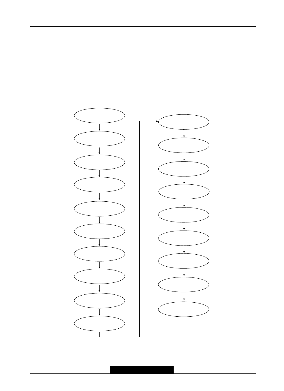
1. White Ba lanc e A djustment
l Refer to adjustment specifications for information on makin g adjustments
m When white balance has to be adjusted during service
- If the module is replaced, it must be readjusted u sing VG -828 equipment,
according to the adjustment spe cifications
- When making progra m upgrades [ ROM (UM04) replacement] or replaci ng A/V
B/D, the values stored i n A/V B /D’s EPROM (UM12) should be written down
and re-ente
The method of white Balane Adjustment before ROM or B/D IS Replaced
red into the new new Rom or A/V Board.
before Rom or B/D is
Replaced
select the Video Mode
Select "Device" from
the menu
Select AD9883
R.G.B-Gain value
R.G.B-Gain value
Factory Mode Exit
Select the pc mode
Enter into the Factory
mode
Select the Device
Select AD9883
R.G.B-Gain value
R.G.B-Gain valye
Enter the Menu+42+
Mute key
Select "White" from the
menu
R.G.B-Gain value
R.G.B-Blas value
Select "Device"
Select FLI2300
Brightness and
Contrast values
Factory Mode Exit
Select the DTV mode
Enter into the Factory
mode
Enter into the
Factory Mode
Separate Record(a)
Separate Record(c)
Separate Record(d)
Separate Record(b)
--1--
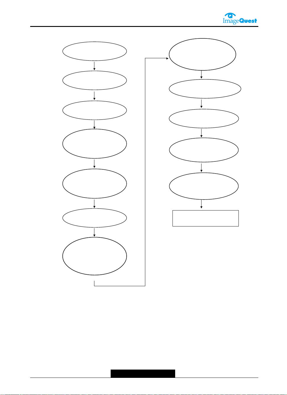
After ROM or B/D
replaced
Select the Video mode
After selecting AD9883
enter(c) Data recorded
in R,G and B-Gain and
Bi as values separately
After exiting from the
Factory select the
PC mode
Enter the Facrory to
select the PC mode
Enter(a) Data recorded
in R.G and B-Gain and
Bias values separately
After selecting AD9883
enter(c) Data recorded in
R.G and B-Gain and Bias
values separately
Completed adjustments of
the White balance
Enter in to the Factory
mode
After selecting "Whte"
enter (a) Data recorded
in Bias values
Separately
After selecting
FLI2300, enter(b) Data
recorded in Brightness
and Contrast values
separately
After exiting from
Factory, select the
DTV mode
After entering into
Factory to select
White enter(a) Data
recorded tn R,G and
B-Gain and Bias
values separately
:When ROM and AV B/D are
replaced without additional
equipment, this is how to
adjust the white balance
--2--

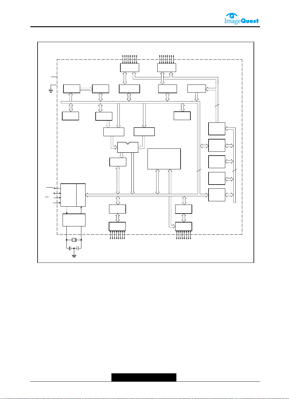
Plasma Display PD421
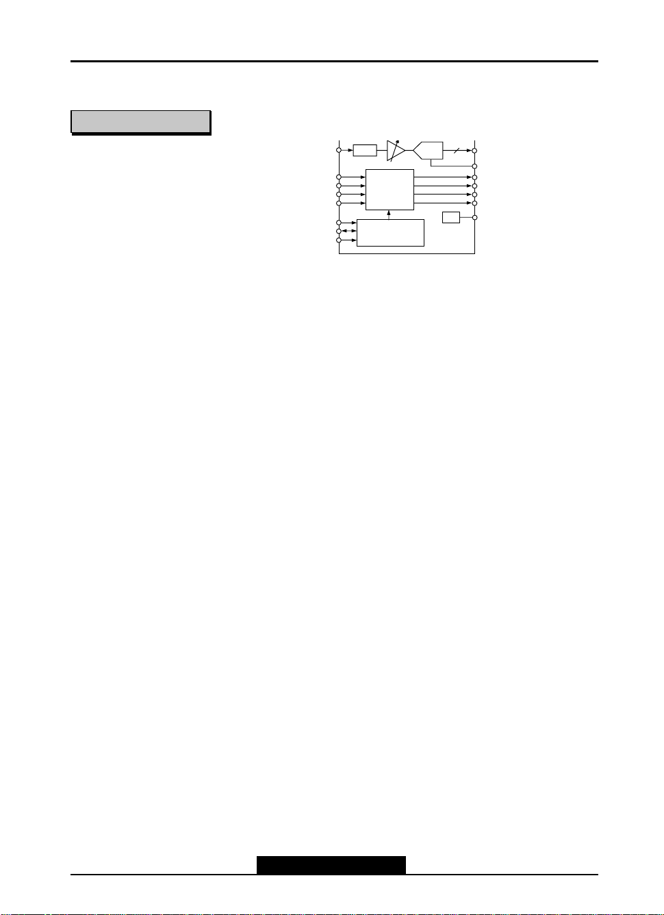
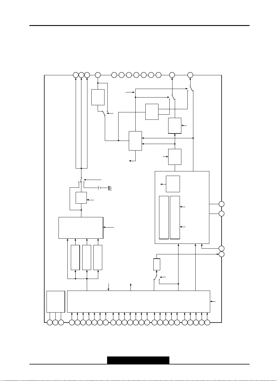
2. A/V Circuit BLOCK Diagram
1) PC Mode
PC inputs, R, G, B, H, and V signals, are entered through D-Sub 15pin
(DSUB1). They are entered into the DTV/ PC sele ction switch, B A7657
(UA01). When PC is selected in M CU, the signals are entered into the AD
converter, AD9883 (UA02).
In AD9883, the signals are c onverted into 24 bits and entered into scaler
ASI500.
BA7657 selec ts PC when pin16 is high and selects DT V when pin 16 is low.
AD9883 is controlled using the SDA/SCL line of pin 57/56.
PC input resolution is fh: 30~70k a nd fv : 50~85Hz, and the ma ximum
resolution is 1080x768 at 85Hz.
If the resolution is above the spe cifications, an out of range message is
displayed on the upper left hand corner of the screen. However, even if the
resolution is within the specified range, if the input timing is different from
the timing indicated on the manual, a ‘not found vesa or out of range ’
message can be displayed. Please check the timing to identify the cause of
the ‘out of range’ message.
PC input sync can rece ive H/V composite or separate, but if DPMS ON is
selected in the PDP menu, DPM S cannot o perate in composite and c an
operate only in separate sync.
The Auto Adjust function, which is used to adjust the picture position and
size, should be carried out in the Windows desktop screen or full cross hatch.
The D TV signals, 480p, 720p, and 1080i, from the set-top box with a D-Sub
out port, can be received through the D-Sub port and displayed in the PC
mode.
DVI Mode
Signals entering through the DVI port (D V101) are converted to 24bits in
the TMDS Receiver, SIL161B (UT02 ), and entered in scalar ASI500.
SIL161B is an output port and is activated when pin number 2 is high.
DTV signa ls 480p, 720p, and 1080i can be displayed through the DVI port .
However, PD421 cannot only display 60Hz DTV signals. It is unable to
display 50Hz DTV signals. PC can support both 50Hz and 60Hz signals.
The resolution of DVI Mode is the same as the PC Mode.
--3--

2) DTV Mode
DTV signals are entered as Y, P b(Cb), and Pr(Cr) component signals,
separated into Y, Cb, Cr , H, and V sync on (xan51AcuxA01) and entered to BA7 657.
If pin 16 is low, DTV signals are entered into ADC9883.
In the AD9883, like the PC signals, the DTV signals are converted to 24 bits
and entered into scalar ASI500.
DTV signa l is composed of 480p (50/60Hz) for SD , 720p (50/60Hz) for HD,
and 1080i (50/ 60Hz). If the video signal, 480i component (DVD component
output), is entered, the screen will not display properly. Also,
because synchronization signal
if the connections are incorrect, it will not operate properly
is in Y singal color Data is in Cr/Cb
3) DVD Mode
DVD signals entered as Y, Pb, and Pr components are applied when entered
as 480i (NT or PAL). 480p DVD signals should be entered through the DTV
component port.
Y, Pb, and P r signals entered through the DVD component port are entered
into the video decoders, Main VPC32 30 (UDM01) and Sub VPC3230 (U DS01),
where they are converted to Y (8bits) and UV (8bits) digital sig nals and sent
to the deinterlacer IC, F L I2310 (UF L1).
UV digital signal means Pb(Cb), and Pr(Cr) signals that have been converted
to digital signals.
The v ideo decoder, VPC3230, automatically detects NTSC and PAL/S ECAM,
identifies them as broadcast signals, converts the interlacer signal into the
progressive signal (fh: 15.7Khz-> 31Khz) in the deinterlacer IC, FLI2310
(UF L1), and sends to the scalar ASI500.
When the PD 421’s main screen is in PC, DVI or DTV mode, the sub-screen
of the PIP or POP function is processed in the Main VI DEO DECODER
(UDM01) and the MODE can be DVD, S-VHS, Video, or Scart.
PIP or POP between video modes is enabled by main video decoder (U DS 01),
sub video decoder (UDS 01), and FIFO memory, MS81V04160 (UF M01). If the
main screen is DVD, then the sub- screen will be S-VHS, Vid eo, or Scart.
Please refer to the table in the back for more information on PIP or POP.
4) S-Video
S-Video signals are entered as Y/ C signals, which is composed of Luminance
--4--

Plasma Display PD421
color signals. The N T S C and P AL /SECAM are automatically detected by the
video decoders, main VPC3230 and sub VPC3230, and converted to Y (8bits)
and UV (8bits) and sent to the deinterla cer IC, FLI2310, as 16bit digital
signal.
S-Video input and co mposite video input share a single audio jack.
Therefore, while the pictures for the two inputs can be viewed at the same
time, only one of the sounds can be heard. PIP/POP operati ons are the same
as described for the DVD mode.
5) Video
Video signal is a composite signal that combines the Luminance (Y) and color
(CHROMA) .
It is entered through the main VPC3230 a nd sub VPC3230 when sele cted in
the input selection switch, TA8851 (UMX01).
If the signal is NTSC, it is first entered into the 3D Comb Filter (filter that
separates the composite to Y/C signal), UPD 64083 (UCF 01) and separated into
Luminance signal Y and color signal, C. The separated signals then enter the
mux switch, TA8851, sent to TA8851 pin44 LU MA IN and pin43 CROMA IN,
and finally sent to Main VPC3230.
When the video input is displayed on the main screen, it passes through the
3D comb filter, but if it is displayed on the s ub- screen (w hen using PIP or
POP), the video input does not pass through the 3D comb filter and i s
displayed using the composite signal.
PAL/SECAM signal cannot be processed by the 3D comb filter. It i s sent as
composite signal to the main VPC3230 and sub VPC3230.
If the signal is NTSC, the video input switch, BF 7654 (UDM02), which is
located in front of the main VPC3230, select the 3D Comb-Y to send the
signal as a Y signal to the VPC 3230. If the signal is Pa l, it selects CVB S to
send the signal as a composite signal to the VPC3230.
Signals entered into VPC3230 are converted to 16bit digital signal (Y (8bits)
and UV (8bits)) and sent to the scalar through the deinterlacer IC, F L I2310.
6) Scart Mode
Scart only supports CV BS signals, which are processed in the same way as
video signals. The RF signal is not supported, and therefore, the Scart pin8
ID signal is ignored.
--5--
Plasma Display PD421
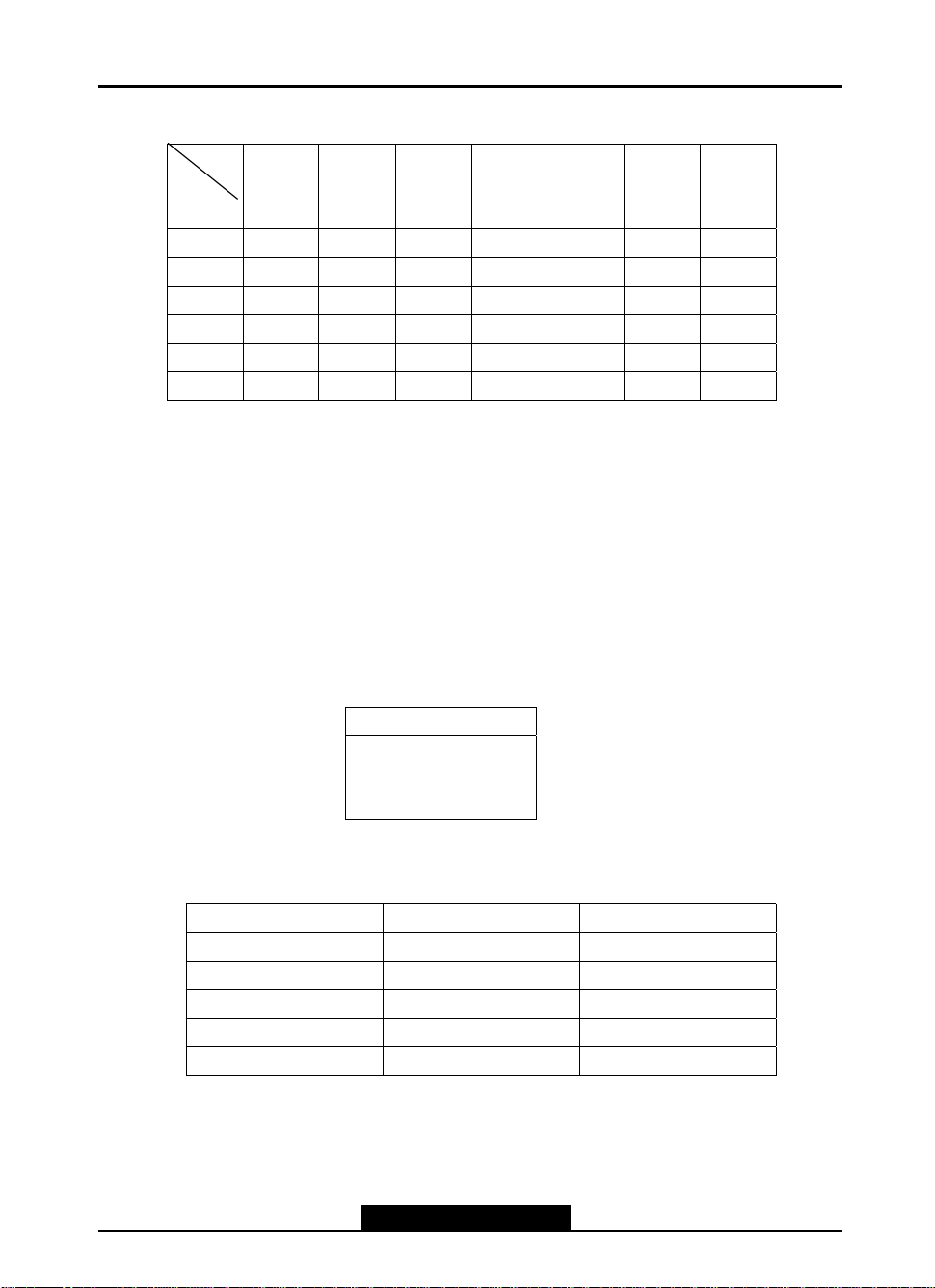
7) PIP/POP Support Mode Map
Sub
Main
PC DTV DVD S-VHS Video Scart DVI
PC X
X
X O X
DTV X X O X
DVD O O O OOO
O
O
O
O
O
O
O
O
O
O
OOO
OOO
OO
S-VHS X O O O
Video X O O
Scart X O
DVI X X O O O O X
X: Not supported, O: Supported
Note: When displaying NTSC or P AL sign als to P IP or POP , if the signals are displayed
as Main: NT SC, Sub: P AL or in reverse, the picture can be seen, but the size scaling for
the sub-scr een will not display properly. This is because the signal is meant for the
main screen. Main screen use s 50Hz PAL or 60Hz NTSC and sub scre en uses 60Hz
NTSC or 50Hz .
8) Scaler Output
Scaler output signals, R, G, a nd B (each 8bits), are outputted as 24bit TTL
signal, converted into LVDS signal in the LVDS converter, DS90C3 85
(ULV01), and sent to the logic B/D in the PDP module. Output timing:
fh : 29.1Khz
fv : PAL 50Hz
NTSC 60Hz
DCLK : about 27Mhz
9) Audio part
Audio input port for each mode:
Input Port Remark
PC/DVI RCA L/R 1E A Shared
DTV RCA L/R 1E A
DVD RCA L /R 1E A
CVBS/S-Video RCA L/R 1E A Shared
Scart cart Jack L /R
S
--6--
Plasma Display PD421
Audio input signal for PC/DVI, DT V, and DV D modes is entered into the
audio processor IC, MSP3450G , and audio input signal for VID E O/S -VIDEO,
and SCART modes is first selected in MUX 8851 a nd entered into the audio
processor.
As in other chips, the audio processor (MSP34 50G) uses the SCL and SDA
line to control volume, and left/right balance and mono/stereo.
The L/ R audio signal sent by MSP3450 is a mplified in the amplifier, TA2 024
(UAU1) and sent to the speaker.
TA2024B support 10W(based on impedance 8Y ) of output for each L/R.
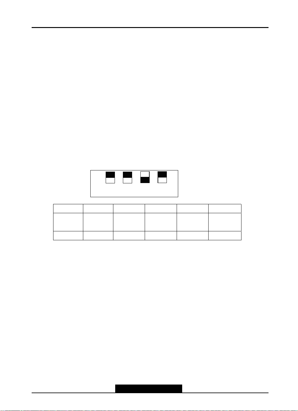
3. Trouble shooting
1) Diagnosing defective module
If the power does not come on or if the module operates abnormally, check
module defect. To do this, remove the rear cover and A/V B/D to revea l the
module’ s logic B/D. The following figure represents the s/w on the logic B/D.
SW 2001
Signal 1 2 Remark
External up up up Forwarding
Criteria
Internal up down
If the switch is set to internal signals, it will operate without external signals,
but the screen will be displayed in full white.
Therefore the module operation can be checked without the A/V board.
Here, be aware that the pin 8 and pin 9 of the power B /D’s CN802(11p),
which is located above the module’s logic B /D, must be shorted and the A/C
power supplied in order for the module to operate normally. Pin 8 is marked
as PS-ON below the connector (CN802).
If module itself is tested and it does not power on or the picture is abnormal,
the module is defective.
When reconnecting the A/V B /D, make sure to change the switch to external
signals.
- The most common module defect is the appearance of a black or br ight
vertical line.
1 2 3 4
4
down
down
up
3
--7--

- Bar
This occ urs when the FPC wire, which connects the address line below the
module, is damaged. Because the wire is on the bottom, it can be e asily
damaged when the module is lifted and assembled or from external shock. Use
caution when handling the module and use the handle on the bottom of the
module to lift or move.
If the vertical bar appears at the same location for all modes, the F PC wire is
damaged.
FPC wire cannot be replaced. The entire module needs to be replaced.
- If the module does not power on, it is mostly likely due to an open fuse on the
power B/D. Check the black and round fuse on the power B/D.
2) Diagnosis by Problem Type
- Power comes on, but the picture does display
Check the AV B/D ’ s communication lines, SDL and SDA lines.
ICs c ontrolled by the S DA and SCL line are ADC9883, F L I2310, MSP 3450G,
VPC3230, 3D comb filter, and TA8851. If after powering on, the SDA and SCL
line’s Vp- p is les s than 4V and checks below 2.5V, the communication line is
loaded at some point. Open and check each IC’ s communication line.
- Can also occur when the connection between the graphic B/D and video B/D is
bad.
- If the picture turns off or the volume is muted while viewing through the set-
top box, please check the status of the set-top box first.
- For abnormal picture when using P IP/POP function, refer to the s ection on
Video Mode in the manual
- If the OSD screen cracks or displays abnormally:
May be caused by bad connection between the graphic B/D’s scaler a nd
SDRAM, K4S643232C (UF B01, UFB02). Use the clea ner to clean the around
the scaler and the UFB01/02.
OSD is processed by the scaler (ASI 500).
- If the power is on and the input signals and connections are normal, but the
picture does not display:
--8--
Plasma Display PD421
B
A
IN
B
OUTA
MIDSCV
SYNC
PROCESSING
AND CLOCK
GENERATION
HSYNC
COAST
CLAMP
FILT
DTACK
HSOUT
VSOUT
SOGOUT
REF
REF
BYPASS
SERIAL REGISTER
AND
POWER MANAGEMENT
SCL
SDA
A
0
AD9883
CLAMP
8
A/D
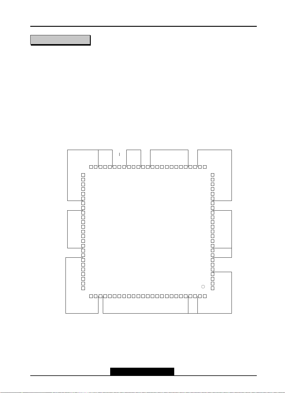
GENERAL DESCRIPTION
The AD9883 is a complete 8-bit, 110 MSPS monolithic analog
interface optimized for capturing RGB graphics signals from
personal computers and workstations. Its 110 MSPS encode
rate capability and full-power analog bandwidth of 300 MHz
supports resolutions up to SXGA (1280X 1024 at 60Hz).
The AD9883 includes a 110 MHz triple ADC with internal
1.25 V reference, a PLL, and programmable gain, offset, and
clamp control. The user provides only a 3.3 V power supply,
analog input, and HSYNC and COAST signals. Three- state
CMOS outputs may be powered from 2.5 V to 3.3 V.
The AD9883’s on-chip PLL generates a pixel clock from HSYNC
and COAST inputs. Pixel clock output freque ncies range from
12 MHz to 110 MHz. PLL clock jitter is 500 ps p-p typical at
10 MSPS. When the COAST signal is presented, the PLL
maintains its output frequency in the absence of HSYNC. A
sampling phase adjustment is provided. Data, HSYNC and
Clock output phase relationships are maintained. The AD9883
also offers full sync processing for composite sync and sync-ongreen applications.
A clamp signal is generated internally or may be provided by the
user through the CLAMP input pin. This interface is fully programmable via a two-wire serial interface.
Fabricated in an advanced CMOS process, the AD9883 is
provided in a space-saving 80-lead LQFP surface mount plastic
ackage and is specifi ed over th e 0 C to 70 C temperature range.
Sync Detect fo Hot ugg ng
Midscale Clamping
Power-Down Mode
Low Power : 500mW tYPICAL
Composite Sync Applications Require an External Coast
Critical Parts Specification
AD9883
MC68HC705BD7B
--9--
AD9883–SPECIFICATIONS
(VD = 3.3 V, V
DD
= 3.3 V, ADC Clock = Maximum Conversion Rate)
Analog Interface
Test AD9883KST-110
Parameter Temp Level Min Typ Max Unit
RESOLUTION 8 Bits
DC ACCURACY
Differential Nonlinearity 25 C I 0.5 +1.25/–1.0 LSB
Full VI +1.35/–1.0 LSB
Integral Nonlinearity 25 C I 0.5 1.85 LSB
Full VI 2.0 LSB
No Missing Codes Full VI Guaranteed
ANALOG INPUT
Input Voltage Range
Minimum Full VI 0.5 V p–p
Maximum Full VI 1.0 V p–p
Gain Tempco 25 C V 100 ppm/C
Input Bias Current 25 C I V 1 A
Full IV 1 A
Input Offset Voltage Full VI 7 50 mV
Input Full-Scale Matching Full VI 6.0 % FS
Offset Adjustment Range Full VI 46 49 52 % FS
REFERENCE OUTPUT
Output Voltage Full VI 1.20 1.25 1.32 V
Temperature Coefficient Full V 50 ppm/C
SWITCHING PERFORMANCE
Maximum Conversion Rate Full VI 110 MSPS
Minimum Conversion Rate Full IV 10 MSPS
Data to Clock Skew Full IV –0.5 +2.0 ns
t
BUFF
Full VI 4.7 s
t
STAH
Full VI 4.0 s
t
DHO
Full VI 0 s
t
DAL
Full VI 4.7 s
t
DAH
Full VI 4.0 s
t
DSU
Full VI 250 s
t
STASU
Full VI 4.7 s
t
STOSU
Full VI 4.0 s
HSYNC Input Frequency Full IV 15 110 kHz
Maximum PLL Clock Rate Full VI 110 MHz
Minimum PLL Clock Rate Full IV 12 MHz
PLL Jitter 25 C I V 400 700
1
ps p-p
Full IV 1000
1
ps p-p
Sampling Phase Tempco Full IV 15 ps/
C
DIGITAL INPUTS
Input Voltage, High (V
IH
) Full VI 2.5 V
Input Voltage, Low (V
IL
) Full VI 0.8 V
Input Voltage, High (V
IH
) Full V –1.0 A
Input Voltage, Low (V
IL
) Full V 1.0 A
Input Capacitance 25 C V 3 pF
DIGITAL OUTPUTS
Output Voltage, High (V
OH
) Full VI V
D
– 0.1 V
Output Voltage, Low (V
OL
) Full VI 0.1 V
Duty Cycle DATACK Full IV 45 50 55 %
Output Coding Binary
--10--

Plasma Display PD421
Test AD9883KST-110
Parameter Temp Level Min Typ Max Unit
POWER SUPPLY
V
D
Supply Voltage Full IV 3.0 3.3 3.6 V
V
DD
Supply Voltage Full IV 2.2 3.3 3.6 V
P
VD
Supply Voltage Full IV 3.0 3.3 3.6 V
I
D
Supply Current (V )
D
5 C V 132 mA
I
DD
Supply Current (V
DD
)
2
25 C V 19 mA
IP
VD
Supply Current (P )
VD
5C V 8 mA
Total Power Dissipation Full VI 525 650 mW
Power-Down Supply Current Full VI 5 10 mA
Power-Down Dissipation Full VI 16.5 33 mW
DYNAMIC PERFORMANCE
Analog Bandwidth, Full Power 25 C V 300 MHz
Transient Response 25 C V 2 ns
Overvoltage Recovery Time 25 C V 1.5 ns
Signal-to-Noise Ratio (SNR) 25 C V 44 dB
(Without Harmonics) Full V 43 dB
f
IN
= 40.7 MHz
Crosstalk Full V 55 dBc
THERMAL CHARACTERISTICS
JC
Junction-to-Case
Thermal Resistance V 16 C/W
JA
Junction-to-Ambient
Thermal Resistance V 35 C/W
NOTES
1
VCO Range = 10, Charge Pump Current = 110, PLL Divider = 1693.
2
DATACK Load = 15 pF, Data Load = 5 pF.
Specifications subject to change without notice.
2
2
--11--
CXA2151Q
Description
The CXA2151Q is a bipolar IC developed for multi
scan TVs, and incorporates a four system video
switch (including HV sync signal processing) and a
YCbCr output matrix circuit.
Features
•Supports the I
2
C bus
•Supports multi scan
•Four system video switch (of which two systems support D3 pins)
•Matrix circuit
•Each YCbCr output can be switched between 0dB, 6dB (gain adjustable) and mute.
•Sync signal automatic identification circuit (with fixed mode)
•Sync separation circuit (supports HD)
•HD Tri-level sync identification circuit
•Sync signal frequency counter (both H and V)
•Dummy sync output
Applications
Multi scan TVs
Structure
Bipolar silicon monolithic IC
Absolute Maximum Ratings(Ta = 25°C, GND1, 2, 3 = 0V)
•Supply voltage V
CC1, 2, 3 –0.3 to +5.5 V
•Operating temperature Topr –20 to +75 °C
•Storage temperature Tstg –65 to +150 °C
•Allowable power dissipation P
D 1400 mW
(when mounted on a 50mm 50mm board)
•Voltage at each pin –0.3 to V
CC1, 2, 3 + 0.3 V
Recommended Operating Conditions
Supply voltage V
CC1, 2, 3 5 ± 0.25 V
48 pin QFP (Plastic)
MC68HC705BD7B
--12--
Block Diagram
30
SCL
31
SDA
32
ADDRESS
27
SEL Y_OUT26SELCB_OUT
25
SELCR_OUT20EXTCLK/XTAL
18
IREF40Vcc148GND128Vcc224GND212Vcc3
6
GND3
22
SELH_OUT
33
IN1_134IN1_235IN1_3
36
IN1_H/L1
37
IN1_V/L2
38
IN1_L3
39
IN1_SW
6dB
YPbPrJ/YCbCr
MATRIX
SELECTOR
6dB
AMP.
YPbPrU/YCbCr
GBR/YCbCr
41
IN2_142IN2_243IN2_3
44
IN2_H/L1
45
IN2_V/L2
46
IN2_L3
47
IN2_SW
1
IN3_12IN3_23IN3_3
4
IN3_H
5
IN3_V
7
IN4_18IN4_29IN4_3
10
IN4_H
11
15 16 13 14
IN4_V
I
2
C BUS
DEC.
IN1 to IN4
SELECTOR
SELSTB_1
SELSTB_2
DECL1_1
DECL2_1
DECL3_1
DECSW_1
DECL1_2
DECL2_2
DECL3_2
DECSW_2
1, 2, 3
HYSW
INPUT_SEL
MAT_OUT
GAIN_SEL
YGAIN
CBGAIN
CRGAIN
YCbCr
EXISTENCE DISTINCTION
INTELLIGENT SYNC SEP .
3-STATE
SYNC
DET.
HSEP_SEL
HD_TC
V_TC
HS_MASK
FIX_SYNC
PRIORITY RANKING
HV > CS > SYNC ON Y/G
3S TATE
MACRO
3
H
V
H_WIDTH
H SYNC
WIDTH
MACRO
VISION
23
SEL V_OUT
DUMMY
SYNC
CLOCK
GEN.
SYNC
COUNTER
H-NUMBER
V-NUMBER
CLK_SEL
SELDUM
H_PH
YG_IN
YG_OUT
V_PH
Plasma Display PD421
--13--
General Description
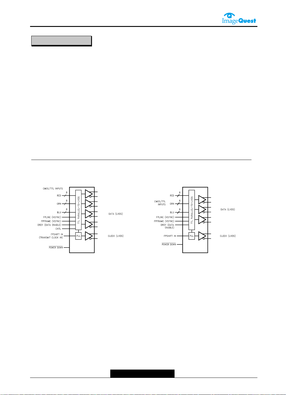
The DS90C385 transmitter converts 28 bits of LVCMOS/
LVTTL data into four LVDS (Low Voltage Differential Signaling) data streams. A phase-locked transmit clock is transmitted in parallel with the data streams over a fifth LVDS link.
Every cycle of the transmit clock 28 bits of input data are
sampled and transmitted. At a transmit clock frequency of 85
MHz, 24 bits of RGB data and 3 bits of LCD timing and
control data (FPLINE, FPFRAME, DRDY) are transmitted at
a rate of 595 Mbps per LVDS data channel. Using a 85 MHz
clock, the data throughput is 297.5 Mbytes/sec. Also available is the DS90C365 that converts 21 bits of LVCMOS/
LVTTL data into three LVDS (Low Voltage Differential Signaling) data streams. Both transmitters can be programmed
for Rising edge strobe or Falling edge strobe through a
dedicated pin. ARising edge or Falling edge strobe transmitter will interoperate with a Falling edge strobe Receiver
(DS90CF386/DS90CF366) without any translation logic.
The DS90C385 is also offered in a 64 ball, 0.8mm fine pitch
ball grid array (FBGA) package which provides a 44 %
reduction in PCB footprint compared to the TSSOP package.
This chipset is an ideal means to solve EMI and cable size
problems associated with wide, high-speed TTL interfaces.
Features
- 20 to 85 MHz shift clock support
- Best±in±Class Set & Hold Times on TxINPUTs
- Tx power consumption
<
130 mW (typ)@85MHz
Grayscale
- Tx Power-down mode
<
200W (max)
- Supports VGA, SVGA, XGA and Single/Dual Pixel
SXGA.
- Narrow bus reduces cable size and cost
- Up to 2.38 Gbps throughput
- Up to 297.5 Megabytes/sec bandwidth
- 345 mV (typ) swing LVDS devices for low EMI
- PLL requires no external components
- Compatible with TIA/EIA-644 LVDS standard
- Low profile 56-lead or 48-lead TSSOP package
- DS90C385 also available in a 64 ball, 0.8mm fine pitch
ball grid array (FBGA) package
Block Diagrams
DS90C385
DS100868-1
Order Number DS90C385MTD or DS90C385SLC
See NS Package Number MTD56 or SLC64A
DS90C365
DS100868-29
Order Number DS90C365MTD
See NS Package Number MTD48
DS90C385
--14--
Plasma Display PD421
Absolute MaximumRatings (Note 1)
If Military/Aerospace specified devices are required,
please contact the NationalSemiconductor Sales Office/
Distributors for availability and specifications.
SupplyVoltage(V
CC
) -0.3V to +4V
CMOS/TTL InputVoltage -0.5V to (V
CC
+ 0.3V)
LVDS DriverOutputVoltage -0.3V to (V
CC
+ 0.3V)
LVDS OutputShort Circuit
Duration Continuous
JunctionTemperature +150 C
Storage Temperature -65 C to +150 C
Lead Temperature
(Soldering,4 sec) +260 C
Solder reflowTemperature
(20 sec for FBGA) +220 C
MaximumPackage Power Dissipation Capacity
@
25 C
MTD56(TSSOP) Package:
DS90C385MTD 1.63 W
MTD48(TSSOP) Package:
DS90C365MTD 1.98 W
SLC64 (FBGA) Package:
DS90C385SLC 2.0 W
Package Derating:
DS90C385MTD 12.5 mW/ C above +25 C
Package Derating:
DS90C365MTD 16 mW/ C above +25 C
DS90C385SLC 10.2mW/ C above+25 C
ESD Rating
(HBM, 1.5kW, 100pF)
>
7kV
(EIAJ, 0W, 200pF)
>
500V
Latch Up Tolerance
@
25 C
>
+/-
300mA
Recommended Operating
Conditions
Min Nom Max Units
SupplyVoltage(V
CC
) 3.0 3.3 3.6 V
Operating Free Air
Temperature(T
A
) -10 +25 +70 C
SupplyNoise Voltage(V
CC
) 100 mV
PP
TxCLKIN frequency 20 85 MHz
Electrical Characteristics
Over recommendedoperatingsupplyand temperaturerangesunless otherwisespecified.
Symbol Parameter Conditions Min Typ Max Units
LVCMOS/LVTTL DC SPECIFICATIONS
V
IH
HighLevel InputVoltage 2.0 V
CC
V
V
IL
Low Level InputVoltage GND 0.8 V
V
CL
InputClamp Voltage ICL= -18 mA -0.79 -1.5 V
I
IN
InputCurrent VIN= 0.4V,2.5V orV
CC
+1.8 +10 A
V
IN
= GND -10 0 A
LVDS DC SPECIFICATIONS
V
OD
DifferentialOutputVoltage RL= 100W 250 345 450 mV
DV
OD
Change in VODbetween
complimentary outputstates
35 mV
V
OS
OffsetVoltage(Note 4) 1.125 1.25 1.375 V
DV
OS
Change in VOSbetween
complimentary outputstates
35 mV
I
OS
OutputShortCircuit Current V
OUT
= 0V, RL= 100W -3.5 -5 mA
I
OZ
OutputTRI-STATE Current Power Down= 0V,
V
OUT
=0VorV
CC
+/-1+/-
10 A
TRANSMITTER SUPPLY CURRENT
ICCTW Transmitter SupplyCurrent
Worst Case
DS90C385
R
L
= 100W,
C
L
= 5 pF,
Worst Case Pattern
(Figures 1, 4)
f = 32.5MHz 31 45 mA
f = 40 MHz 32 50 mA
f = 65 MHz 37 55 mA
f = 85 MHz 42 60 mA
ICCTG Transmitter Supply Current
16 Grayscale
DS90C385
R
L
= 100W,
C
L
= 5 pF,
16 Grayscale Pattern
(Figures 2, 4)
f = 32.5MHz 29 38 mA
f = 40 MHz 30 40 mA
f = 65 MHz 35 45 mA
f = 85 MHz 39 50 mA
ICCTW TransmitterSupply Current
Worst Case
DS90C365
R
L
= 100W,
C
L
= 5 pF,
Worst Case Pattern
(Figures 1, 4)
f = 32.5MHz 28 42 mA
f = 40 MHz 29 47 mA
f = 65 MHz 34 52 mA
f = 85 MHz 39 57 mA
o
o
o
o
o
o
o
o
o
o
--15--
Electrical Characteristics(Continued)
Over recommended operating supply and
temperature rangesunless otherwise specified.
Over recommended operating supply and
temperature rangesunless otherwise specified.
Over recommended operating supply and
temperature rangesunless otherwise specified.
Symbol Parameter Conditions Min Typ Max Units
TRANSMITTER SUPPLY CURRENT
ICCTG TransmitterSupply Current
16 Grayscale
DS90C365
R
L
= 100W,
C
L
= 5 pF,
16 Grayscale Pattern
(Figures 3, 4)
f = 32.5MHz 26 35 mA
f = 40 MHz 27 37 mA
f = 65 MHz 32 42 mA
f = 85 MHz 36 47 mA
ICCTZ TransmitterSupply Current
Power Down
Power Down = Low
DriverOutputsin TRI-STATE under
Power Down Mode
10 55 A
Note 1: ™Absolute Maximum Ratings"are those values beyondwhichthe safetyof thedevice cannotbe guaranteed.Theyare not meantto implythatthe device
shouldbe operatedat these limits.The tablesof ™Electrical Characteristics" specify conditionsfor deviceoperation.
Note 2: Typicalvalues are givenforV
CC
= 3.3Vand TA= +25C.
Note 3: Current intodevice pins is definedas positive.Currentout of devicepins is definedas negative.Voltages are referencedto groundunless otherwise
specified(exceptV
OD
and D
V
OD
).
Note 4: V
OS
previously referredas VCM.
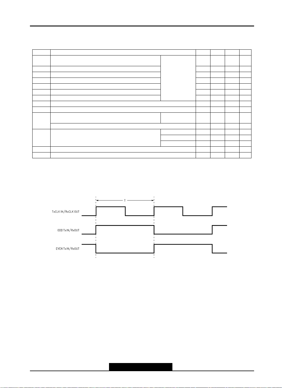
Recommended Transmitter Input Characteristics
Symbol Parameter Min Typ Max Units
TCIT TxCLK IN TransitionTime
(Figure 6)
1.0 6.0 ns
TCIP TxCLK IN Period
(Figure 7)
11.76 T 50 ns
TCIH TxCLK IN HighTime
(Figure 7)
0.35T 0.5T 0.65T ns
TCIL TxCLK IN Low Time
(Figure 7)
0.35T 0.5T 0.65T ns
TXIT TxIN TransitionTime 1.5 6.0 ns
Transmitter Switching Characteristics
Symbol Parameter Min Typ Max Units
LLHT LVDS Low-to-HighTransitionTime
(Figure 5)
0.75 1.5 ns
LHLT LVDS High-to-LowTransitionTime
(Figure 5)
0.75 1.5 ns
TPPos0 TransmitterOutputPulse Positionfor Bit 0
(Figures 13, 14)
(Note 5)
f = 40 MHz -0.25 0 0.25 ns
TPPos1 TransmitterOutputPulse Positionfor Bit 1 3.32 3.57 3.82 ns
TPPos2 TransmitterOutputPulse Positionfor Bit 2 6.89 7.14 7.39 ns
TPPos3 TransmitterOutputPulse Positionfor Bit 3 10.46 10.71 10.96 ns
TPPos4 TransmitterOutputPulse Positionfor Bit 4 14.04 14.29 14.54 ns
TPPos5 TransmitterOutputPulse Positionfor Bit 5 17.61 17.86 18.11 ns
TPPos6 TransmitterOutputPulse Positionfor Bit 6 21.18 21.43 21.68 ns
TPPos0 TransmitterOutputPulse Positionfor Bit 0
(Figures 13, 14)
(Note 5)
f = 65 MHz -0.20 0 0.20 ns
TPPos1 TransmitterOutputPulse Positionfor Bit 1 2.00 2.20 2.40 ns
TPPos2 TransmitterOutputPulse Positionfor Bit 2 4.20 4.40 4.60 ns
TPPos3 TransmitterOutputPulse Positionfor Bit 3 6.39 6.59 6.79 ns
TPPos4 TransmitterOutputPulse Positionfor Bit 4 8.59 8.79 8.99 ns
TPPos5 TransmitterOutputPulse Positionfor Bit 5 10.79 10.99 11.19 ns
TPPos6 TransmitterOutputPulse Positionfor Bit 6 12.99 13.19 13.39 ns
--16--
Plasma Display PD421
Transmitter Switching Characteristics (Continued)
Over recommended operating supply and temperature ranges unless otherwise specified
Symbol Parameter Min Typ Max Units
TPPos0 TransmitterOutputPulse Positionfor Bit 0
(Figures 13, 14)
(Note 5)
f = 85 MHz -0.20 0 0.20 ns
TPPos1 TransmitterOutput Pulse Position for Bit 1
TransmitterOutput Pulse Position for Bit 2
TransmitterOutput Pulse Position for Bit 3
TransmitterOutput Pulse Position for Bit 4
TransmitterOutput Pulse Position for Bit 5
TransmitterOutput Pulse Position for Bit 6
1.48 1.68 1.88 ns
TPPos2 3.16 3.36 3.56 ns
TPPos3 4.84 5.04 5.24 ns
TPPos4 6.52 6.72 6.92 ns
TPPos5 8.20 8.40 8.60 ns
TPPos6 9.88 10.08 10.28 ns
TSTC TxIN Setup to TxCLK IN
(Figure 7)
2.5 ns
THTC TxIN Hold to TxCLK IN
(Figure 7)
TCCD TxCLK IN to TxCLK OUT Delay
(Figure 8)
TA= 25 C, V
CC
= 3.3V
3.8
0
6.3 ns
ns
TxCLK IN toTxCLK OUT Delay
(Figure 8)
2.8 7.1 ns
TJCC TransmitterJitter Cycle-to-Cycle
(Figures 15, 16)
(Note 6) f = 85 MHz 110 150 ps
f = 65 MHz 210 230 ps
f = 40 MHz 350 370 ps
TPLLS Transmitter Phase Lock Loop Set
(Figure 9)
10 ms
TPDD Transmitter Power DownDelay
(Figure 12)
100 ns
Note 5: The Minimumand MaximumLimits are based on statisticalanalysisof the device performanceover process,voltage, and temperatureranges. This
parameteris functionality testedonlyon AutomaticTest Equipment(ATE).
Note 6: Thelimitsare basedon benchcharacterization of the device'sjitterresponseoverthe powersupplyvoltagerange.Outputclockjitteris measured witha
cycle-to-cyclejitterof+/˛3nsappliedtothe inputclocksignalwhiledata inputsare switching(See Figures 15and 16).A jittereventof 3ns,represents worsecase
jumpinthe clockedgefrommostgraphicscontroller VGA chipscurrently available.This parameteris usedwhencalculatingsystemmarginas described inAN-1059.
AC Timing Diagrams
DS100868-4
FIGURE 1. ™Worst Case∫ Test Pattern (Note 7)
--17--

DESCRIPTION
The P89C51RB2/RC2/RD2 device contains a non-volatile
16kB/32kB/64kB Flash program memory that is both parallel
programmable and serial In-System and In-Application
Programmable. In-System Programming (ISP) allows the user to
download new code while the microcontroller sits in the application.
In-Application Programming (IAP) means that the microcontroller
fetches new program code and reprograms itself while in the
system. This allows for remote programming over a modem link.
A default serial loader (boot loader) program in ROM allows serial
In-System programming of the Flash memory via the UART without
the need for a loader in the Flash code. For In-Application
Programming, the user program erases and reprograms the Flash
memory by use of standard routines contained in ROM.
This device executes one machine cycle in 6 clock cycles, hence
providing twice the speed of a conventional 80C51. An OTP
configuration bit lets the user select conventional 12 clock timing
if desired.
This device is a Single-Chip 8-Bit Microcontroller manufactured in
advanced CMOS process and is a derivative of the 80C51
microcontroller family. The instruction set is 100% compatible with
the 80C51 instruction set.
The device also has four 8-bit I/O ports, three 16-bit timer/event
counters, a multi-source, four-priority-level, nested interrupt structure,
an enhanced UART and on-chip oscillator and timing circuits.
The added features of the P89C51RB2/RC2/RD2 makes it a
powerful microcontroller for applications that require pulse width
modulation, high-speed I/O and up/down counting capabilities such
as motor control.
FEATURES
- 80C51 Central Processing Unit
- On-chip Flash Program Memory with In-System Programming
(ISP) and In-Application Programming (IAP) capability
- Boot ROM contains low level Flash programming routines for
downloading via the UART
- Can be programmed by the end-user application (IAP)
- 6 clocks per machine cycle operation (standard)
- 12 clocks per machine cycle operation (optional)
- Speed up to 20 MHz with 6 clock cycles per machine cycle
(40 MHz equivalent performance); up to 33 MHz with 12 clocks
per machine cycle
- Fully static operation
- RAM expandable externally to 64 kB
- 4 level priority interrupt
- 7 interrupt sources
- Four 8-bit I/O ports
- Full-duplex enhanced UART
± Framing error detection
± Automatic address recognition
- Power control modes
± Clock can be stopped and resumed
± Idle mode
± Power down mode
- Programmable clock out
- Second DPTR register
- Asynchronous port reset
- Low EMI (inhibit ALE)
- Programmable Counter Array (PCA)
± PWM
± Capture/compare
P89C51RD2BA
--18--

Plasma Display PD421
ORDERING INFORMATION
PHILIPS
(EXCEPT NORTH
PHILIPS NORTH
MEMORY
TEMPERA TURE
FREQUENCY (MHz)
AMER CA)
PART ORDER
NUMBER
PART MARKING
AMER CA
PART ORDER
NUMBER
FLASH RAM
RANGE (5C)
AND PACKAGE
VOLTAGE
RANGE
6 CLOCK
MODE
12 CLOCK
MODE
DWG #
1 P89C51RB2HBA P89C51RB2BA 16 kB 512 B 0 to +70, PLCC 4.5±5.5 V 0 to 20 MHz 0 to 33 MHz SOT187-2
2 P89C51RB2HBBD P89C51RB2BBD 16 kB 512 B 0 to +70, LQFP 4.5±5.5 V 0 to 20 MHz 0 to 33 MHz SOT389-1
3 P89C51RC2HBP P89C51RC2BP 32 kB 512 B 0 to +70, PDIP 4.5±5.5 V 0 to 20 MHz 0 to 33 MHz SOT129-1
4 P89C51RC2HBA P89C51RC2BA 32 kB 512 B 0 to +70, PLCC 4.5±5.5 V 0 to 20 MHz 0 to 33 MHz SOT187-2
5 P89C51RC2HFA P89C51RC2FA 32 kB 512 B ±40 to +85, PLCC 4.5±5.5 V 0 to 20 MHz 0 to 33 MHz SOT187-2
6 P89C51RC2HBBD P89C51RC2BBD 32 kB 512 B 0 to +70, LQFP 4.5±5.5 V 0 to 20 MHz 0 to 33 MHz SOT389-1
7 P89C51RC2HFBD P89C51RC2FBD 32 kB 512 B ±40 to +85, LQFP 4.5±5.5 V 0 to 20 MHz 0 to 33 MHz SOT389-1
8 P89C51RD2HBP P89C51RD2BP 64 kB 1 kB 0 to +70, PDIP 4.5±5.5 V 0 to 20 MHz 0 to 33 MHz SOT129-1
9 P89C51RD2HBA P89C51RD2BA 64 kB 1 kB 0 to +70, PLCC 4.5±5.5 V 0 to 20 MHz 0 to 33 MHz SOT187-2
10 P89C51RD2HBBD P89C51RD2BBD 64 kB 1 kB 0 to +70, LQFP 4.5±5.5 V 0 to 20 MHz 0 to 33 MHz SOT389-1
I
I
--19--
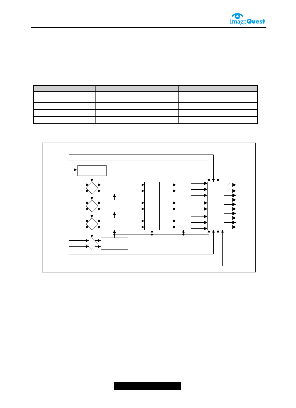
BLOCK DIAGRAM
SU01065
PSEN
EAV
PP
ALE
RST
XTAL1 XTAL2
V
CC
V
SS
POR T 0
DRIVERS
POR T 2
DRIVERS
RAM ADDR
REGISTER
RAM
POR T 0
LATCH
POR T 2
LATCH
FLASH
REGISTER
B
ACC
STACK
POINTER
TMP2
TMP1
ALU
TIMING
AND
CONTROL
INSTRUCTION
REGISTER
PD
OSCILLATOR
PSW
POR T 1
LATCH
POR T 3
LATCH
POR T 1
DRIVERS
POR T 3
DRIVERS
PROGRAM
ADDRESS
REGISTER
BUFFER
PC
INCRE-
MENTER
PROGRAM
COUNTER
DPTR'S
MULTIPLE
P1.0±P1.7
P3.0±P3.7
P0.0±P0.7 P2.0±P2.7
SFRs
TIMERS
P.C.A.
8
8 16
--20--

Plasma Display PD421
DESCRIPTION
The s2300 is a highly integrated digital video
format converter for DTV and DVD applications
using patented deinterlacing and post
processing algorithms from Faroudja
Laboratories, coupled with highly flexible
scaling, a wide variety of aspect ratio
conversions, and other special video enhancing
features to produce the highest quality image.
INPUTS
–
Input all industry standard and non-standard
video resolutions, including 480i (NTSC),
576i (PAL/SECAM), 480p, 720p, 1080i, and
VGA to SXGA
Digital input, 8-bit Y/Cr/Cb (ITU-R BT656),
8-bit Y/Pr/Pb, 16-bit Y Cr/Cb (ITU-R BT601),
24-bit RGB, YCrCb, YPrPb
Input pixel rate up to 75MHz maximum
OUTPUTS
–
Output resolutions include 480p, 576i, 576p,
720p, 1080i, 1080p, and VGA to SXGA
Interlaced or Progressive output
Output can be either analog YUV/RGB
(through the integrated 10-bit DAC), or
digital 24-bit RGB, YCrCb, YPrPb (4:4:4), or
digital 16/20-bit Y Cr/Cb (4:2:2)
Output pixel rate up to 150MHz maximum
FORMATS
–
Input color manipulation matrix supports all
color spaces: RGB, YPrPb, 4:4:4 YCrCb,
4:2:2 YCr/Cb, ITU-R BT656, ITU-R BT601
Output supports analog RGB, YPrPb,
YCrCb, and digital RGB, YPrPb, 4:4:4
YCrCb, 4:2:2 YCr/Cb
FRONT END PROCESSING
–
Motion Adaptive Noise Reduction - Improves
picture quality for off-air material.
Cross Color Suppressor (CCS) - Removes
cross color artifacts in composite video
signals due to poor Y/C separation in
standard 2D video decoders, eliminating the
need for expensive 3D video decoders.
DEINTERLACING
–
Per-pixel Motion Adaptive Deinterlacing
Patented FilmMode Processing - Used for
proper de-interlacing of 3:2 and 2:2 pulldown
material.
Edit Correction - Film content is continuously
monitored for any break in sequence caused
by “bad edits” and quickly compensates for
the most effective reduction in artifacts.
DCDi™ - Video is analyzed on a single pixel
granularity to detect presence or absence of
angled lines and edges, which are then
processed to produce a smooth & natural
looking image without visible artifacts or
“jaggies”.
SCALING
–
High Quality Fully Programmable Two
Dimensional Scaler
Aspect Ratio Conversion for “Anamorphic”
or “Panoramic” (non-linear)
Display 4:3 images on 16:9 displays and
vice versa, including Letterbox to Fullscreen,
Pillarbox, and Subtitle Display Modes
TrueLife™ ENHANCER
–
Two dimensional, non-linear, luma & chroma
video enhancer brings out details in the
picture, producing a more life-like image.
MEMORY
–
32-bit wide SDRAM (i.e. one 2Mx32bit, or
two 1Mx16bit), up to 166MHz operation
FRC
–
Tearless Frame Rate Conversion,
50/60/72/75/100/120 Hz
S2310
--21--

FIGURE 1: Packaging and Pinout Information
Package: 208-pin PQFP
ja = TBD °C/watt
Input Processor
with Auto Sync
and auto Adjust
Noise Reducer,
Deinterlacer, Frame
Rate Converter and
SDRAM interface
Port 2
8-bit
656 Input
Port 1
8/16/24-bit
RGB/YCrCb
Input
Clock
Generation
PLLs
2Mx32
SDRAM
(external)
Vertical and
Horizontal
Scalers
Vertical and
Horizontal
Enhancers
Output
Processor with
Sync Generation
and DACs
16/20/24-bit
RBG/YCrCb
Digital Outputs
RBG/YCrCb
Analog Outputs
--22--
Plasma Display PD421
General Description Features
The SiI 161B receiver uses PanelLink Digital technology to support hi gh
resolution displays up to UXGA. The SiI 161B receiver supports up to true
color panels (24 bit/pixel, 16.7M colors) in 1 or 2 pixels/clock mode. In
addition, the receiver data output is time st aggered to reduce ground bounce
that affects EMI. A ll PanelLink products are designed on a scaleable CMOS
architecture. This ensures s upport for future performance requirem ents while
maintaining the same logic al interfac e. W it h this scalabl e architect ure, system
designers can be assured that the interfac e will be fixed through a number of
technology and performance generations.
PanelLink Digital tec hnology simplifies PC and display interface design
by resolving many of the system level issues associated with high-speed
mixed signal design, providing the system des igner with a digital interface
solution that is quicker to market and lower in cost.
• Low Power Operation: 280m A max. current
consumption at 3.3V core operation
• Time staggered data output for reduced ground
bounce
• Sync Detect: for Plug & Display “Hot P l uggi ng”
• Cable Distance Support: over 5m with twisted-pair,
fiber-optics ready
• ESD tolerant to 5kV(HBM on all pins )
• Compliant with DVI 1.0 (DVI is back wards
compatible with VESA
®
P&DTM and DFP)
• Hsync Dejitter Circuitry
• Low power standby mode with clock detect ci rcuitry
SiI 161B
Pin Diagram
HS_DJTR
1
SiI 161B
100-Pin TQFP
(Top V iew)
PD
2
ST
3
PIXS
4
GND5
VCC
6
STAG_OUT7
SCDT
8
PDO
9
QE0
10
QE1
11
QE2
12
QE3
13
QE4
14
QE5
15
QE6
16
QE7
17
OVCC
18
OGND
19
QE8
20
QE9
21
QE1022
QE11
23
QE1224
QE13
25
QE1426QE1527OGND28OVCC29QE1630QE1731QE1832QE1933QE2034QE2135QE2236
QE2337VCC38GND39CTL140CTL241
CTL342OVCC43ODCK44
OGND45DE46VSYNC47HSYNC48QO049
QO1
50
75
QO21
74
QO20
73
QO19
72
QO18 71
QO17
70
QO16 69
GND
68
VCC
67
QO15
66
QO14
65
QO13
64
QO12
63
QO11
62
QO10
61
QO9
60
QO8
59
OGND
58
OVCC
57
QO7
56
QO6
55
QO5 54
QO4
53
QO3 52
QO2
51
QO22
OCK_INV
100
RESERVED
99
PGND
98
PVCC
97
EXT_RES
96
AVCC
95
RXC-
94
RXC+
93
AGND
92
RX0-
91
RX0+ 90
AGND
89
AVCC
88
AGND
87
RX1-
86
RX1+ 85
AVCC
84
AGND
83
AVCC 82
RX2-
81
RX2+
80
AGND
79
OVCC
78
QO23 77
OGND
76
DIFFERENTIAL SIGNAL
ODD 8-bits RED
EVEN 8-bits RED
ODD 8-bits GREEN
EVEN 8-bits GREEN
ODD 8-bits BLUE
EVEN 8-bits BLUE
CONFIG. PINS
PLL
PWR
MANAGEMENT
GPO
OUTPUT CLOCK
CONTROLS
Sil161B
MC68HC705BD7B
--23--
Silicon Image, Inc.
Differences Between SiI161A and SiI161B
While the SiI161B is pin to pin compatible with the SiI161A, there are minor differences in funct ions and suggested external component
value. When designing the SiI161B int o an existi ng design, note that the recommended external resistor (E XT_RES) value has changed from
560 to 390 to match the impedance of a 50 cable. Pin 1 of the SiI161A functions as a selection between Single Link and Dual Link
mode. The SiI161B does not support Dual Link operation. Instead pin 1 is used to enable or disable the HSYNC Dejitter function. Table 1 lists
the differences between SiI161A and SiI161B.
Pin/Function SiI161A SiI161B
Pin 1 S_D: to select Single/Dual Link mode. Pull high to
select Dual Link and Pull low for Single Link.
HS_DJTR: to enable HSYNC Dejitter circuitry.
Pull high to enable, Pull low to disable.
Pin 4 PIXS/M_S PIXS
Pin 7 STAG_OUT/SYNCO STAG_OUT
EXT_RES Resistor Value 560 390
Table 1. SiI161A vs. SiI161B pin differences.
Functional Block Diagram
CTL3
RX2+
RX2-
RX1+
RX1-
RX0+
RX0-
RXC+
RXC-
SYNC2
EXT_RES
PDO
ST
ODCK
PIXS
HS_DJTR
OCK_INV
STAG_OUT
Data Recovery
CH2
VCR
Termination
Control
Data Recovery
CH1
VCR
Data Recovery
CH0
VCR
PLL
VCR
SYNC1
SYNC0
Channel
SYNC
SYNC2
SYNC1
SYNC0
Decod er
CTL2
CTL1
VSYNC
HSYNC
Panel
Inter-
face
Logic
QE[23:0]
24
QO[23:0]
24
DE
HSYNC
VSYNC
CTL3
CTL2
CTL1
SCDT
DATA
DATA
DATA
--24--
Plasma Display PD421
Y
TA2024
MC68HC705BD7B
GENERAL DESCRIPTION
The TA2024 is a 15W/ch continuous average two-channel Class-T Digital Audio
Power Amplifier IC using Tripath’s proprietary Digital Power Processing™
technology. Class-T amplifiers offer both the audio fidelity of Class-AB and the
power efficiency of Class-D amplifiers.
APPLICATIONS
" Computer/PC Multimedia
" DVD Players
" Cable Set-Top Products
" Televisions
" Video CD Players
" Battery Powered Systems
BENEFITS
" Fully integrated solution with FETs
" Easier to design-in than Class-D
" Reduced system cost with no heat sink
" Dramatically improves efficiency versus Class-
AB
" Signal fidelity equal to high quality linear
amplifiers
" High dynamic range compatible with digital
media such as CD, DVD, and Internet audio
TYPICAL PERFORMANCE
10
5
2
1
0.5
0.2
THD+N (%)
0.1
0.05
0.02
0.01
VDD = 12V
f = 1kHz
Av = 12
BW = 22Hz - 22kHz
THD+N versus Output Power
1 2 5 10 20500m
Output Power (W)
RL= 4YRL= 8Y
FEATURES
" Class-T architecture
" Single Supply Operation
" “Audiophile” Quality Sound
" 0.04% THD+N @ 9W, 4Y
" 0.18% IHF-IM @ 1W, 4Y
" 11W @ 4Y , 0.1% THD+N
" 6W @ 8Y , 0.1% THD+N
" High Power
" 15W @ 4Y , 10% THD+N
" 10W @ 8Y , 10% THD+N
" High Efficiency
" 81% @ 15W, 4Y
" 88% @ 10W, 8Y
" Dynamic Range = 102 dB
" Mute and Sleep inputs
" Turn-on & turn-off pop suppression
" Over-current protection
" Over-temperature protection
" Bridged outputs
" 36-pin Power SOP package
--25--
ABSOLUTE MAXIMUM RATINGS
(Note 1)
S YMBOL P ARAM ETER Value UNITS
V
DD
S upply Voltage 16 V
V5 Input S ection Supply Voltage 6.0 V
S LE E P S LE E P Input Voltage -0.3 to 6.0 V
MUTE MUTE Input Voltage -0.3 to V5+0.3 V
T
STOR E
S torage Temperature Range -40 to 150
C
T
A
Operating Free-air Temperature Range 0 to 70
C
T
J
J unction Temperature 150
C
Note 1 : Absolute Maximum Ratings indicate limits beyond which damage to the device may
Note 2 : See Power Dissipation Derating in the Applications Information section.
OPERATING CONDITIONS
(Note 4)
S YMB OL P AR AME TE R MIN. TYP . MAX. UNITS
V
DD
S upply Voltage 8.5 12 13.2 V
V
IH
High-level Input Voltage (MUTE, SLE E P ) 3.5 V
V
IL
Low-level Input Voltage (MUTE, SLEEP) 1 V
Note 3: Recommended Operating Conditions indicate conditions for which the device is func
See Electrical Characteristics for guaranteed specific performance limits.
ELECTRICAL CHARACTERISTICS
See Test/Application Circuit. Unless otherwise specified, VDD = 12V, f = 1kHz, Measurem
Bandwidth = 22kHz, R
L
= 4Y, TA = 25 q C, Package heat slug soldered to 2.8 square-inch P
SYM B OL P ARAME TER CONDITIONS MIN. TYP . MAX. UNITS
P
O
Output Power
(Continuous Average/Channel)
THD+N = 0.1% R
L
= 4
R
L
= 8
THD+N = 10% R
L
= 4
R
L
= 8
9
5.5
12
8
11
6
15
10
W
W
W
W
I
DD,MUTE
Mute Supply Current MUTE = VIH 5.5 7 mA
I
DD, SL EE P
S leep Supply Current S LE E P = VIH 0.25 2 mA
I
q
Quiescent Current VIN = 0 V 61 75 mA
THD + N Total Harmonic Distortion Plus
Noise
PO = 9W/Channel 0.04 %
IHF-IM IHF Intermodulation Distortion 19kHz, 20kHz, 1:1 (IHF) 0.18 0.5 %
S NR S ignal-to-Noise Ratio
A-W eighted, P
OUT
= 1W, RL = 8
89 dB
CS Channel Separation 30kHz Bandwidth 50 55 dB
PS RR P ower Supply Rejection Ratio Vripple = 100mV. 60 80 dB
j
Power Efficiency
P
OUT
= 10W/Channel, RL = 8
88 %
V
OFFSET
Output Offset Voltage No Load, MUTE = Logic Low 50 150 mV
VOH High-level output volt age
(FAULT & OVER LOAD)
3.5 V
VOL Low-level output voltage
(FAULT & OVER LOAD)
1 V
e
OUT
Output Noise Voltage A-W eighted, input AC grounded 100
o
V
Note: Minimum and maximum limits are guaranteed but may not be 100% tested.
o
o
o
--26--
Plasma Display PD421
PIN DESCRIPTION
TA2024 PINOUT
FAULT
PGND2
NC
NC
VDD2
OUTM2
OUTM1
VDD1
NC
VDDA
NC
PGND1
CPUMP
DCAP2
AGND3
BIASCAP
IN2
VP2
MUTE
IN1
VP1
V5A
AGND2
OVERLOADB
REF
AGND1
V5D
DCAP1
30
19
20
21
22
23
24
25
26
27
28
29
1
15
14
13
11
10
12
9
8
7
6
5
4
3
2
36-pin Power SOP Package
(Top View)
16
17
18
+5VGEN
36
31
32
33
34
35
OUTP1
VDD1
VDD2
OUTP2
DGND
NC
SLEEP
Pin Function Description
2, 3 DCAP2, DCAP1 Charge pump sw itching pins. DCAP1 (pin 3) is a free running 300kHz square
wave betw een VDDA and DGND (12Vpp nominal). DCAP2 (pin 2) is level shifted
10 volts above DCAP1 (pin 3) w ith the same amplitude (12Vpp nominal),
frequency , and phase as DCAP1.
4, 9 V5D, V5A Digital 5VDC, Analog 5VDC
5, 8,
17
AGND1, AGND2,
AGND3
Analog Ground
6 REF Internal reference voltage; approximately 1.0 VDC.
7 OVERLOADB A logic low output indicates t he input signal has overloaded the amplifier.
10, 14 VP1, VP2 Input stage output pins.
11, 15 IN1, IN2 Single-ended inputs. Inputs are a “virtual” ground of an inverting opamp w ith
approximately 2.4VDC bias.
12 MUTE When set to logic high, both amplifiers are muted and in idle mode. When low
(grounded), both amplifiers are fully operational. If left floating, the device stay s in
the mute mode. This pin should be tied to GND if not used.
16 BIASCAP Input stage bias voltage (approximately 2.4VDC).
18 SLEEP When set to logic high, device goes into low power mode. If not used, this pin
should be grounded
19 FAULT A logic high output indicates thermal overload, or an output is shorted to ground,
or another output.
20, 35 PGND2, PGND1 Pow er Grounds (high current)
22 DGND Digital Ground
24, 27;
31, 28
OUTP 2 & OUTM2;
OUTP 1 & OUTM1
Bridged outputs
25, 26,
29, 30
VDD2, VDD2
VDD1, VDD1
Supply pins for high current H-bridges, nominally 12VDC.
13, 21,
23, 32,
34
NC Not connected. Not bonded internally .
33 VDDA Analog 12VDC
36 CPUMP Charge pump output (nominally 10V above VDDA)
1 5VGEN Regulated 5VDC source used to supply power to the input section (pins 4 and 9).
--27--
APPLICATION /TEST CIRCUIT
TA2024
R
L
4Y or *8Y
MUTE
FAULT
OVERLOADB
(+12V)
C
I
2.2uF
VP1
VP2
IN1
IN2
OUTP1
OUTM1
OUTP2
OUTM2
VDDA
+5VGEN
BIASCAP
DCAP2
DCAP1
C
I
2.2uF
C
A
0.1uF
C
D
0.1uF
CPUMP
10
11
20
1
33
29
26
7
19
31
28
24
27
36
2
3
15
14
12
16
R
F
20KY
18
R
Z
10Y."1/2W
R
Z
10Y."1/2W
C
Z
0.47uF
C
P
1uF
+
+
5V
SLEEP
5V
5V
+12V
0.1uF
REF
R
REF
8.25KY, 1%
6
1megY
All Diodes Motorola MBRS130T3
* Use Co = 0.22oF for 8 Ohm loads
VDD1
PGND1
VDD1
PGND1
VDD2
VDD2
PGND2
PGND2
Note: Analog and Digital/Power Grounds must
be connected locally at the TA2024
C
S
0.1uF
C
S
0.1uF
To Pin 1
4
5
V5D
8
AGND1
AGND2
V5A
22
C
S
0.1uF
DGND
VDD1
PGND2
35
PGND1
180uF, 16V
VDD2
VDD
+
+
+
Processing
&
Modulation
Processing
&
Modulation
*C
o
0.47uF
L
o
10uH, 2A
9
(Pin 8)
Analog Ground
Digital/Power Ground
(Pin 35)
(Pin 35)
(Pin 20)
(Pin 20)
To Pins 4,9
R
I
20KY
(Pin 8)
R
F
20KY
R
I
20KY
AGND3
17
180uF, 16V
C
SW
C
SW
*C
o
0.47uF
L
o
10uH, 2A
R
L
4Y or *8Y
L
o
10uH, 2A
L
o
10uH, 2A
*C
o
0.47uF
*C
o
0.47uF
C
Z
0.47uF
C
SW
0.1uF
C
SW
0.1uF
C
S
0.1uF
D
O
D
O
D
O
D
O
C
CM
0.1uF
C
CM
0.1uF
(Pin 35)
(Pin 20)
13
NC
21
23
25
30
32
34
VDD1
VDD2
--28--
Plasma Display PD421
TA8851
MC68HC705BD7B
--29--
 Loading...