

Hyundai h pdp4201 schematic

PDP TELEVISION
SERVICE MANUAL
MODEL NO. H-PDP4201
Hyundai
Please read this manual carefully before service.
1

CONTENTS
PartⅠ:PP06 Chassis Features and Circuit………
PartⅡ:Introduction on Circuit Functions of PT4206 ……
PartⅢ:Analysis on Signal Process of PT4206………
PartⅣ:Typical Defectives and Repair of PT4206…………
Annex: 1、Main Assembly DrawingⅠ&Ⅱ of PT4206
2、Wire Connecting Drawing of PT4206
2
PartⅠ:PP06 Chassis Features and CBU Contents
1.1、PP06 Chassis Technical Specifications:
1.1.1 PT4206 Panel Datas
PT4206 is the most typical model using PP06 chassis; therefore we take PT4206 as an example.
PDP Panel Resolution
Colors 16,777,216
Dot Pitch
Brightness High brightness
Contrast High contrast
Lifespan of Panel 20000 Hours
V iewing Angle
Response Time
Remarks: Brightness and contrast may vary because of different panels being used.
PT4206 mainly uses SAMSUNG SDI panel model S42SD-YD04 or S42SD-YD05 注
1.1.2 Specification Sheet
852×3(RGB)×480
1.095mm(H)×1.110mm(V)
U/D:160 / L/R:160
933mm(H)×533mm(V)
3

PC
Recommended Input Format
Unsupportable Input Format
Indication
640×480/60Hz
800×600/60Hz
Yes
Color Temp. Adjust. Yes
Quick Plug-In & Use Yes
Picture Location Adjust.
Yes
HD Signal
YPbPr)
(
HD Signal
DVI)
(
Compatible with
Compatible with
Picture System PAL/NTSC/SECAM
Video
Including
(
S-Video)
Sound System
Digital Comb Filter Yes
3D Comb Filter(NTSC)
Movement Compensation Function Yes
Output Voltage
Audio Effect WOW
Audio
NICAM/IGR Yes
Video/YpbPr Audio Input Audio L/R
PC/DVI Audio Input Audio L/R
Input Voltage 220V~, 50Hz
Rating
Consumption
Standby
Consumption
400W
≦
≦
480P、576P、720P 、1080i
480P、576P、720P
1080i and HDTV
D/K、I、B/G、M
Yes
2×5W
3W
、
1.2、Main Features:
1.2.1 T erm inals
RF Input 1(Rear)
S Terminal Input 1(Rear)
A/V Input RCA,1(Rear)
YCbCr RCA,1(Rear)
DTV YPbPr RCA,1(Rear)
VGA/SVGA Input Hi-Density D-SUB 15 pin connector,1(Rear)
DVI Input 1 Rear
A/V Output RCA, Rear
Remarks: PT4206 is equipped with a service terminal, which service people can connect with
PC RS232 terminal to upgrade the software.
1.2.2 Working Condition Requirement:
Working Condition Requirement Temperature 0℃~40℃
4
Humidity 20﹪~70﹪
Altitude 0-2000m
1.2.3 Others
Tuning System FS Tuning,236 Programs
NICAM Demodulation Yes
Audio Effect Process AV stereo、SRS WOW,5 Bands Equalizer
Picture Freeze TV/AV/S-VIDEO/YcbCr Only
On Screen Display Chinese/English, Menu Location movable by user.
Blue Background without Signal Yes
Power Saving When TV is connected with PC input, while there is
no signal from PC, after 60 seconds, TV will be
automatically off and enter into Power Saving Mode.
Press any key on TV or R/C, or there is signal from
PC again, TV will be switched on automatically.
Pixel Movement When this function is on, pictures will move on
regularly to protect the screen.
White Screen Display When this function is on, the screen will be
completely white to clear up slight shadows(please
see the instruction manual for more details)
Home/Commercial Mode Optional Users can choose between 15 minutes auto-off without
signal or 3 hours auto-off without operation(please
see the instruction manual for more details)
1.3、CBU Content
1.3.1 PDP Inside Drawing:
⑥
5
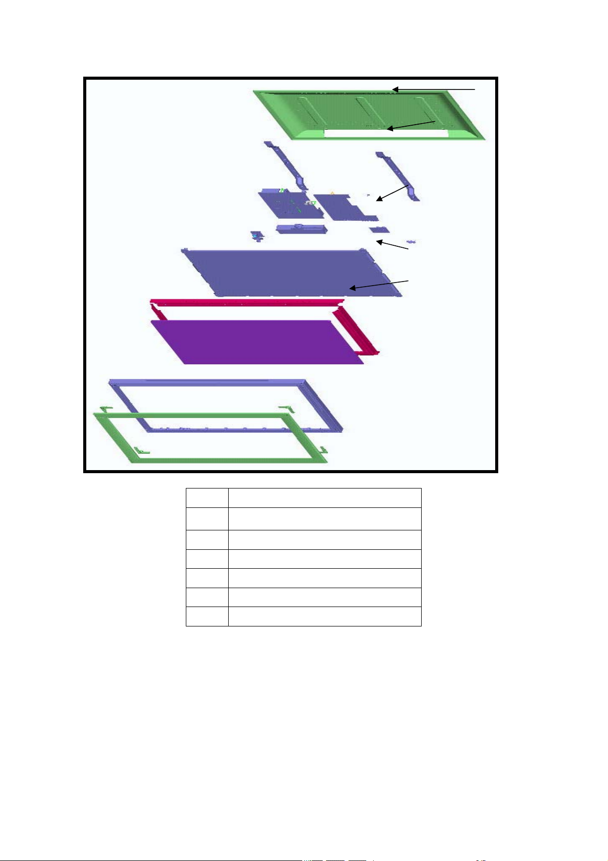
⑤ ⑤
④ ④
③ ③
② ②
① ①
ial No. Name
① Front Cabinet
② Filter Glass
③ Shelve Bar
④ PDP Panel Module
⑤ Down Cover Module etc.
⑥ Back Cabinet
Remarks: This drawing is for references only, please see the main assembly diagram
and wire-connecting diagram for details.
1.3.2 Circuit Content:
6
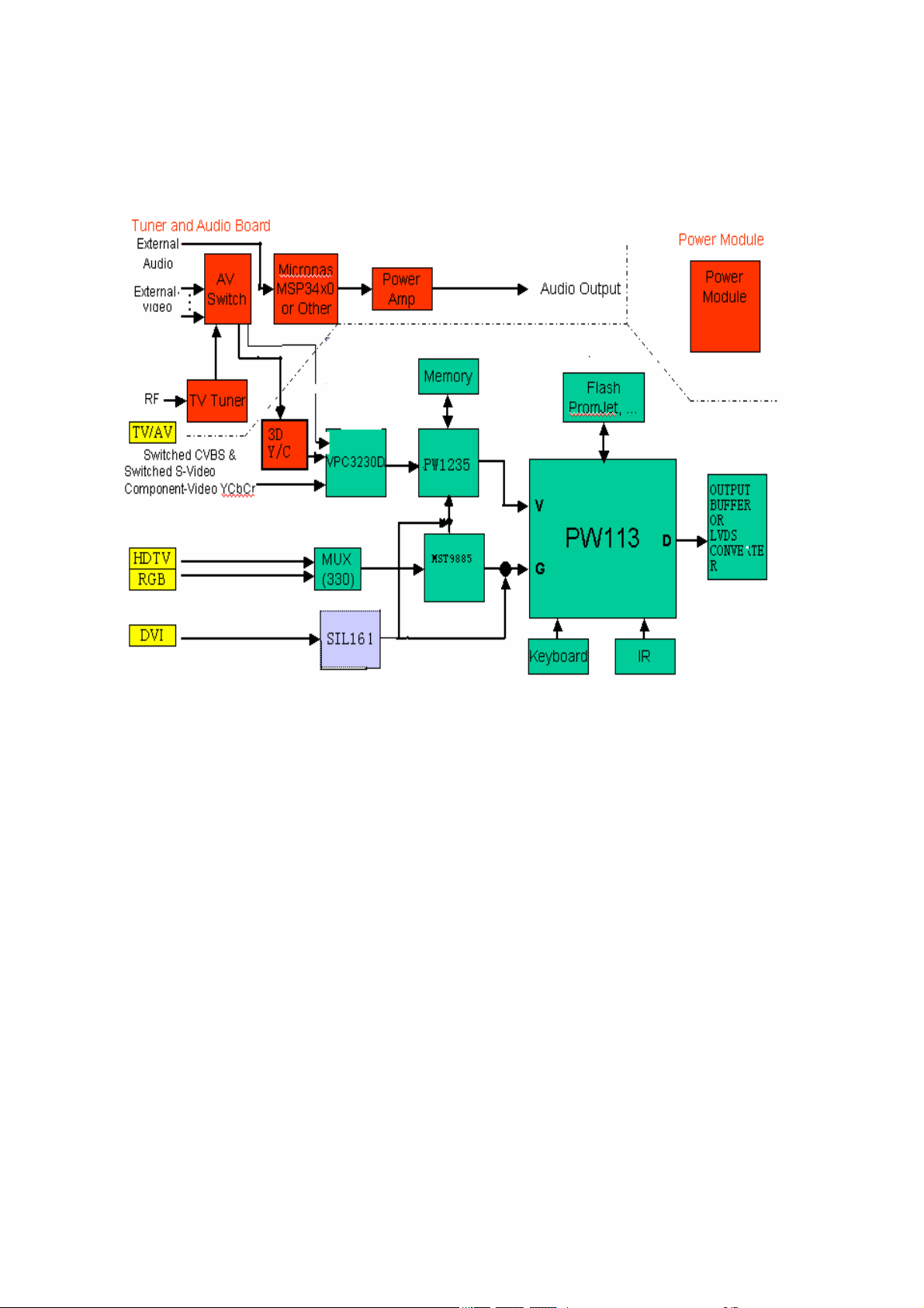
The main content of PP06 circuit include: Power Regulating Circuit, RF Circuit, VGA,
Analog Video, Digital Video Signal Processing Circuit, System Control Circuit, Button Control
Circuit. Reference drawing as below:
PartⅡ:Introduction on Circuit Functions of PT4206
7
2.1 Changhong PDP TV PT4206 main IC functions:
NO. NAME TYPE
1 N901 TDQ-6F7-FM2W
2 N601 MSP3410G-C12-100
3 U705 TA2024
4 U701 uPD64083GF-3BA NTSC 3D comb filter
5 N902 TEA6425D AV video switch
6 U1 VPC3230D-QA-B3 Digital video disposal
7 U6 MST9885 A/D converter
8 U11 SiI161BCT100 DVI signal disposal
9 U16 PW113-20Q Format transform and MCU
10 U17 AM29LV800BT-90 FLASH ROM
11 U22 DS90C383AMTD Difference transmit
12 U20 ST232CD RS-232 signal disposal
13 U7 24LC21A/SN
14 U9/U13 SN74LVC126AD Suffer amplifier
15 U71 74LV32D Sync. face lifting enlarge
16 U8 24LC21A/SN
17 U19 24LC32A/SN
18 U4 IS42S16400(A)-7T SDRAM
19 U5 PI5V330(Q) RGB/YpbPr switch
20 U3 PW1235 IP transform and picture improve
Unify tuner
Sound disposal
sound amplifier
E²PROM(display parameter information)
E²PROM(DVI parameter information)
E²PROM(user control information)
Function
2.2、Changhong PDP TV PT4206 main IC functions introduction:
2.2.1 A/D converter MST9885 General:
The MST9885 is a fully integrated analog interface for digitizing high-resolution RGB
graphics signals from PCs and workstations. With a sampling rate capability of up to 140 MHz,
it can accurately support display resolutions up to 1280x1024 (SXGA) at 75 Hz. The clamped
input circuits provide sufficient bandwidth to accurately digitize each pixel.
The MST9885B provides a high performance highly integrated solution to support the
digitization process, including the ADCs, a voltage reference, a PLL to generate the pixel
sampling clock from HSYNC, clamping
circuits, and programmable offset and gain circuits to provide brightness and contrast controls.
When the COAST signal is asserted, the PLL will maintain its output frequency when HSYNC
pulses are absent, such as during the VSYNC period in some systems.
A 32-step programmable phase adjustment control (0-360 deg) is provided for the pixel
sampling clock to adjust for the difference between the HSYNC edge and RGB pixel edge
timing.
The MST9885B can send output data through one 24-bit port at the pixel clock rate.
The MST9885B can also support R, G, B to Y, U, V conversion.
The MST9885B has internal programmable pattern generator for testing.
The MST9885B can accept either standard TTL, CMOS levels or sawtooth vertical deflection
signals for VSYNC input.
8
MST9885 Pin Function Descriptions:
Pin(s) name Function
70~77 RED0~RED7
2~9 GREEN0~GREEN7
12~19 BLUE0~BLUE7
Red output data
Green output data
Blue output data
67 DATACK Output data clock
66 HSOUT HSYNC output
65 SOGOUT Sync-on- Green Slicer output
64 VSOUT VSYNC output
37 MIDSCV Internal mid-scale voltage bypass
58 REFBYP Internal reference bypass
31 VSYNC Vertical SYNC input
30 HSYNC Horizontal SYNC input
43 BAIN Blue analog input
49 SOGIN Sync-on- Green analog input
48 GAIN Green analog input
54 RAIN Red analog input
29 COAST Hold PLL frequency and do not track HSYNC
38 CLAMP
External clamp input(we connect it to ground )
55 A0 Serial interface address pin
56 SCL
57 SDA
2
C bus(clock)
I
2
C bus(data)
I
33 FILT PLL connect to external filter
26,27,39,
AVDD Analog power
42,45,46,
51,52,59,
62
11,22,23,
V33 Digital output power
69,78,79
34,35
1,10,20,
PVDD PLL power
GND ground
21,24,25,
28,32,36,
40,41,44,
47,50,53,
60,61,63,
68,80
9

MST9885 Block Diagram:
2.2.
2、VPC3230 General:
VPC3230 Pin Function Descriptions:
Pin No. Pin Name Short Description
1~3
4~6
7,64,30,
11,12,25,
35,65,77,
46,51,68,
80
8 NC NC
9 VSUPCAP Supply Voltage, Digital Decoupling Circuitry
10,29,36,
45,52
59,69,76
13 SCL I2C Bus Clock
14 SDA I2C Bus Data
15 RESQ Reset Input
16 TEST Test Pin
17 VGAV VGAV Input
18 YCOEQ Y/C Output Enable Input
19~23
24 CLK20 Main Clock Output
27 LLC2 Clock Output
28 LLC1 NC
31~34 Y0~Y7
R1G1B1IN RGB Analog Component Input 1
R2G2B2IN RGB Analog Component Input 2
GND GND
V33 Supply Voltage, Digital Circuitry
AVCC Analog Voltage
FFIE NC
YUV signal output (Digital ITU-R656 format)
10

37~40
41~44
C0~C7
Digital chromatic signal output
47~50
53 INTLC Interlace scan control output (0-odd,1-even)
54 AVO Active Video Output
55 FSY/HC NC
56 MSY/HS Horizontal Sync Pulse output
57 VS Vertical Sync Pulse
58 FPDAT NC
60 CLK5 5 MHz Clock Output
61 NC NC
62 XTAL1 20.25M Analog Crystal Input
63 XTAL2 20.25M Analog Crystal Output
66 VRT Reference Voltage Top, Analog
67 I2CSEL I2C Bus Address Select
70 VOUT Analog Video Output
71 CIN Chroma / Analog Video 5 Input
72 VIN1 Video 1 Analog Input
73 VIN2 Video 2 Analog Input
74 VIN3 Video 3 Analog Input
78 VREF Reference Voltage Top
79 FB1IN Fast Blank Input
VPC3230 Block Diagram:
11

2.2.3、PW113 General:
The PW113 integrates an industry-leading scaler, an advanced OSD engine, a flexible input
port system, system memory, and a powerful 80186-based ,horizontal and vertical image scaler
swith intelligent Auto Image Optimization circuitry。The Image Processor supports NTSC or PAL
video data with a 4:3 aspect ratio and 16:9 aspect ratio sources, such as DVD or HDTV. Video
Input formats can be in either YUV4:4:4 (24 bit) or YUV4:2:2 (16 bit) input modes。The PW113
uses an integrated PLL to synchronize the display interface timing to the input timing。An
integrated OSD controller supports sophisticated bit-mapped based OSDs The OSD controller
supports transparent, translucent, and fade-in/ fade-out functions.
Pin Function Descriptions:
Pin(s) name Function
Video Port Pin Descriptions
71 VCLK VPort Pixel Clock input
74 VVS VPort Vertical Sync input
75 VHS VPort Horizontal Sync input
69 VFIELD VGPort Field Input
70 VPEN VPort Pixel Enable
47~56 YUV0~YUV7 VGPort ITUR656 Pixel Data.,I/O port。
We use : 47 MUTE mute control 、 48 PW1230E
PW1235output enable、49 VGASEL VGA/YpbPr select、
50 S1 sound system control、51 DVIPD DVI interface
standby、54 STANDBY power standby control、56 RST1
peripheral IC reset
Graphics Port Pin Descriptions
31 GCLK GPort Pixel Clock input
32 GVS GPort Vertical Sync input
33 GHSSOG GPort Horizontal Sync/GPort Sync- on-Green input
34 GPEN GPort Pixel Enable input
35 GFBK GPort PLL Feedback / Line Advance Input
20~27 GRE0~GRE7
10~15,18,19 GGE0~GGE7
2~9 GBE0~GBE7
GPort Red Pixel Data input
GPort Green Pixel Data input
GPort Blue Pixel Data input
Display/Graphics Port Pin Descriptions
129~136
119~122,
125~128
DGR0~DGR7
DGG0~DGG7
111~118 DGB0~DGB7
DGPort Red Pixel Data(odd outputs)
DGPort Green Pixel Data(odd outputs)
DGPort Blue Pixel Data(odd outputs)
Display Port Pin Descriptions
106 DCLK DPort Pixel Clock output
108 DVS DPort Vertical Sync output
109 DHS DPort Horizontal Sync output
110 DEN DPort Pixel Enable output
96~103 DR0~DR7
88~95 DR0~DR7
76~83 DB0~DB7
DPort Red Pixel Data(even outputs)
DPort Green Pixel Data(even outputs)
DPort Blue Pixel Data(even outputs)
12
Microprocessor Interface Pin Descriptions
194 WR Write Enable low indicates a write to external RAM or other
devices
195 RD Read Enable low indicates a read to external RAM or other
devices
196 ROMOE ROM Output Enable low output indi cates a read from
external ROM.
197 ROMWE ROM Write Enable low indicates a write to external ROM.
198 CS0 Chip select signal
199 CS1 Chip select signal
193 NMI Non-maskable Interrupt
164,173~
A1~A19
Microprocessor address bus output bits
184,187~
192
148~163 D0~D15
Microprocessor 16-bit bidirectional data bus
Peripheral Interface Pin Descriptions
207 PORTA0 DISPEN signal output(PDP display control)
206 PORTA1
READY signal input(PDP display ready)
205 PORTA2 SDA
204 PORTA3 SCL
203 PORTA4 IR receive signal input
201 PORTA6 DVI digital interface select control
203 PORTA4 IR receive signal input
57、58、60~
64
PORTB0 ~
PORTB7
Key control input
39 PORTC0 MA-EN enable control
40 PORTC1 480ISEL 480I anti-copy control
41 PORTC2 RST-1235 PW1235 reset
42 PORTC3 DIGSEL DVI digital interface select
43 PORTC4 LVDSON LVDS enable control
44 PORTC5 S0 sound system control
45、46 PORTC6 、
LED control
PORTC7
67 RXD Serial Receive Data
68 TXD Serial Transmit Data
Miscellaneous Pin Descriptions
142 TEST Test mode enable
139 RESET Bidirectional reset pin
169 XI Crystal input
170 XO Crystal output
Power and Ground Pin Descriptions
16,37,65,84,137,185
17,38,66,85,138,186
29,52,72,86,104,123,
VDD1 1.8V digital core power.
VSS Digital core ground
VDDQ3 3.3V digital I/O power.
140,171,208
1,30,53,73,87,105,124,
VSSQ Digital I/O ground.
141,172
165 VDDPA2 1.8V analog clock generator power.
166 VSSPA2 Clock generator analog ground.
167 VDDPA1 1.8V analog clock generator power.
168 VSSPA1 Clock generator analog ground.
13
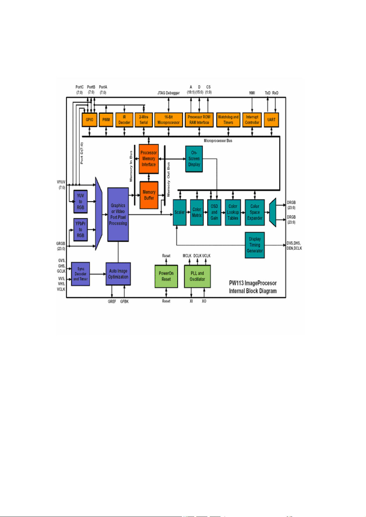
PW113 Block Diagram
14

2.2.4、PW1235 General
PW1235 supports standard digital video signal , incorporates deinterlacing、
scaling .the PW1235 is able to effectively deinterlace video input by creating motion vectors that
follow frame-to-frame movement, and provide clear, progressive output in both analog and digital
formats. The PW1235 integrates input interface、MEMORY control circuit、picture improve、
output interface circuit、I
2
C bus interface and so on,all the function are controlled by I2C bus。
Pin Function Descriptions:
Pin(s) Name Function
Video Port Pin Descriptions
27 PVVS Primary Video (PV) Port vertical sync input.
28 PVHS Port horizontal sync input
25 PVCLK Port pixel clock input
26 CREF Video input clock reference
12 SVVS Port (ITU-R BT656 format) vertical sync input
11 SVHS Port (ITU-R BT656 format) horizontal sync input
13 SVCLK Port (ITU-R BT656 format) pixel clock input
30~33、35~38 VR0~VR7
15~18、20~23 VG0~VG7
1~4、6~9 VB0~VB7
Video port red data input
V ideo port green data input
V ideo port blue data input
Digital/Graphics (DG) Port Pins
68 DGCLK Digital/Graphics (DG) port pixel clock
67 DGVS
Digital/Graphics (DG) port vertical sync.
66 DGHS Digital/Graphics (DG) port horizontal sync
91、92、94、95、
DGR0~DGR7
Digital/Graphics (DG) port red data
97~100
81~84,86~89 DGG0~DGG7
70~73,75、76、
DGB0~DGB7
Digital/Graphics (DG) port green data.
Digital/Graphics (DG) port blue data
78、79
Analog Display Port Pin Descriptions
156
153
ADR Analog display port red (V/Pr) data
ADG Analog display port green (Y/Y) data
150 ADB Analog display port blue (U/Pb) data
161 VREFIN Reference voltage input.
162 VREFOUT Reference voltage output.
159 RSET Full-Scale adjust resistor
160 COMP Compensation pin
Digital Display Output Port Pin Descriptions
102 DCLK Digital display output port pixel clock
103 DVS Digital display output port vertical sync
104 DHS Digital display output port horizontal sync.
108 DENR Display pixel enable red/Vertical blanking period
(VBLANK)
106 DENG Display pixel enable green
107 DENB Display pixel enable blue/Horizontal blanking period
(HBLANK)
145 DEN Digital display output port output enable
132、133、
DR0~DR7
Digital display output port red data
135、136、
138、139、
15
141、142
121、122、
DG0~DG7
124、125、
127~130
110 、 111 、
DB0~DB7
113 、 114 、
116~119
Memory Pin Descriptions
229 MCLK SDRAM clock
223 MCLKFB SDRAM clock feedback
225 MRAS SDRAM row address strobe
226 MCAS SDRAM column address strobe
227 MWE SDRAM write enable
213、210、207、204、
203、206、209、211、
MA0 ~
MA13
214、217、215、220、
221、218
255、252、248、245、
242、239、236、232、
MD0 ~
MD15
231、234、238、241、
244、247、250、254
Host Interface Pin Descriptions
47 2WDAT SDA
45 2WCLK SCL
43 2WA1 Programmable two-wire serial bus address bit 1
44 2WA2 Programmable two-wire serial bus address bit 2
178、179、181~186 MCUD0 ~
MCUD7
168~170、172~
PORTB1 MCU address bus
174、176、177
190 MCUCS Chip select
191 MCUWR MCUR/W signal
192 MCUCMD MCU command signal
188 MCURDY MCU Ready signal
Miscellaneous Pin Descriptions
56 TEST Test mode
144 TESTCLK Used for testing, can be used to supply display clock
55 RESETn Hardware asynchronous reset.
40 XTALI Crystal oscillator input
41 XTALO Crystal oscillator output
146 CGMS CGMS Enable
201 MVE Macrovision write protected enable
62, 63, 194,195 NC
System Power Pin Descriptions
5, 34, 93, 123,140,
VDD Digital core power (2.5V).
175,205, 235
19, 49, 77, 112,
VSS Digital core ground.
134, 187, 219, 251
Digital display output port green data.
Digital display output port blue data.
SDRAM address bus
SDRAM data bus
MCU data bus
16
 Loading...