

Page 1
Service manual
LCD
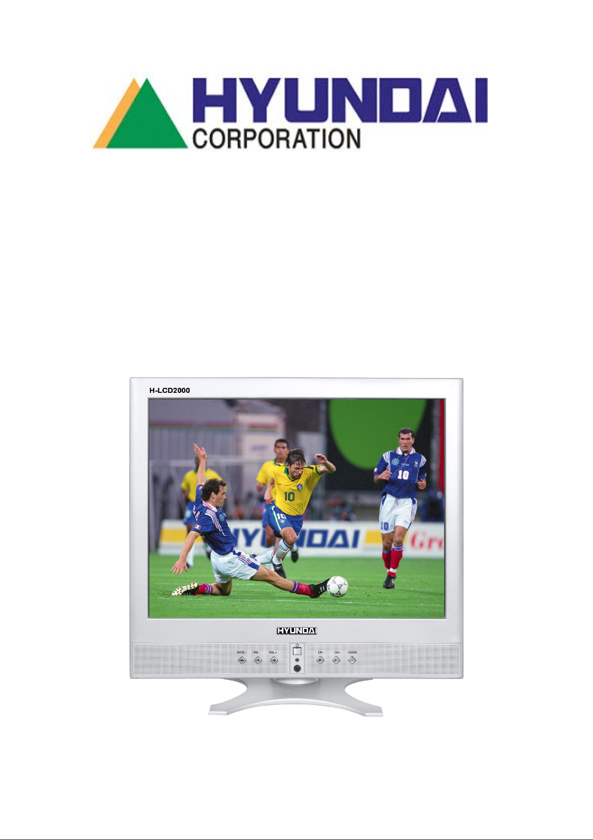
Model: H-LCD2000
VER 1.1
Prepared Frolov V. 201204
Page 2
H-LCD2000Service Manual Page 1 of 57
SPECIFICATIONS
Items Specifications
Size (diagonal) 20.1 inch
High Brightness
High Contrast
Wide Angle of View
LCD panel
Recommended Resolution 800X600
Dot Pitch 0. 5mm(H) x0. 5mm (V)
Number of Dots 800xRGBx600
Viewable Area 408.0mm(H) x306.0mm (V)
Qualified Signal Sources VGA
SmartScaling YES
PC
Video
(including
S-Video)
Audio
Power
Standard Power Consumption
Standby Power Consumption
Appearance
Designs and specifications are subject to change without notice.
Auto Color Temperature YES
Smart Tracking YES
Color Display 16.7millon
Qualified Systems PAL, NTSC, SECAM
PAL System Digital Comb Filter YES
Sport Compensatory Function YES
Audio Output 2x2W
Audio Input
VGA Audio Input Headphone audio input
LCD TV Voltage Input DC 12V/18V
AC Adapter Voltage Input 160-240V~ 50Hz
AC Adapter Voltage Output DC 12V/18V
Model of Specialized AC Adapter CH-1218R
Main Body Color Silver gray
Unit Dimension
Unit Weight Approximately 8.8kg
High Speed Response
Long Lamp Life
Audio Left/Right (Av and S-Video use in
community)
≤55W
≤5W
464mm(L)×211mm(W) ×471mm(H)
1
Page 3

H-LCD2000Service Manual Page 2 of 57
SAFETY INSTRODUCTIONS AND MAINTENANCE
All instructions must be read and understand well before you operating this product.
Heed all warnings and follow all instructions.
Please use the attachment recommended by the manufacturer. Use the inadequate
attachments may result in accidents.
Please adjust the product through the panel buttons or the remote control, do not
remove the cover or attempt to service the product by yourself.
Do not place the product on an unstable cart, stand, tripod, bracket, or table. The
product may fall, causing serious personal injuries as well as the damage to the
product.
Unplug the power cord from the AC outlet when the product is unused for long
periods of time or during a lightning storm.
Protect the power cord from being walked on or pinched particularly at plugs to avoid
the electric shock. When unplug the plug, always hold the wide slot, do not touch the
metal part.
Do not expose the remote control to shock, liquids, and do not place it in an area with
high humidity. Please use the qualified batteries and do not mix batteries with
different types. Do not mix old and new batteries, and do not place the batteries to fire
or disassemble them. If the remote control is unused for an extend period of time,
remove batteries from the remote control.
Place the signal cord back of the product.
Unplug the power cord from the AC outlet before cleaning the product. Do not use
liquid cleaners or aerosol cleaners; use the special LCD Panel cleaners. Keep the
power off before LCD panel dry completely.
Do not use volatile cleaners or you may damage the LCD Panel/Covers.
Do not overexert or touch the panel when you convey the product.
Caution: Over-press the panel may destroy the product.
To ensure not to get an electric shock or short circuit, please do not spill liquid or other
objects into the product.
Please place the product on a flat surface in a well-ventilated location. Keep it away
from the burning-light, high-temperature, and humidity. Store the product with a
temperature from –20℃ ~50℃; Otherwise you may destroy the product.
The temperature of the product’s body will become a little higher after a long period
use. This phenomenon indicates that the product is exhausting the quantity of heat in
normal working mode, but please do not let children or anyone who is sensitive of
temperature to touch.
Unplug the power cord from the AC outlet and contact our service personnel to repair
under the following conditions:
A. When a liquid has been spilled or objects have fallen into the product.
B. Although you have operated the product by following the operating instructions, it
still cannot work normally.
C. Any obvious abnormality in the product.
Install your LCD TV in a room where direct sunlight will not fall upon the screen.
2
Page 4
H-LCD2000Service Manual Page 3 of 57
Allow enough space (at least 10cm) between the TV and the wall for proper
ventilation.
It is recommended to watch the LCD TV in a soft and indirect light. The optimum
watching distance is 5-7 times of the screen’s vertical height.
Note: All the OSD and illustrations in this manual may be somewhat different from the
actual situation. Please take the LCD Color TV as the standard.
CAUTION!
The AC adapter supplied for this product is for indoor use only; please do not spill liquid or
other objects into the product, do not cover or press the body of the AC adapter with
anything, and do not pull or pluck the wire when you use the product. Please do not use
the wire, which has been snapped for any reasons.
omponents
This is an international hazard symbol, telling you that the c
identified by the symbol have special safety-related characteristics.
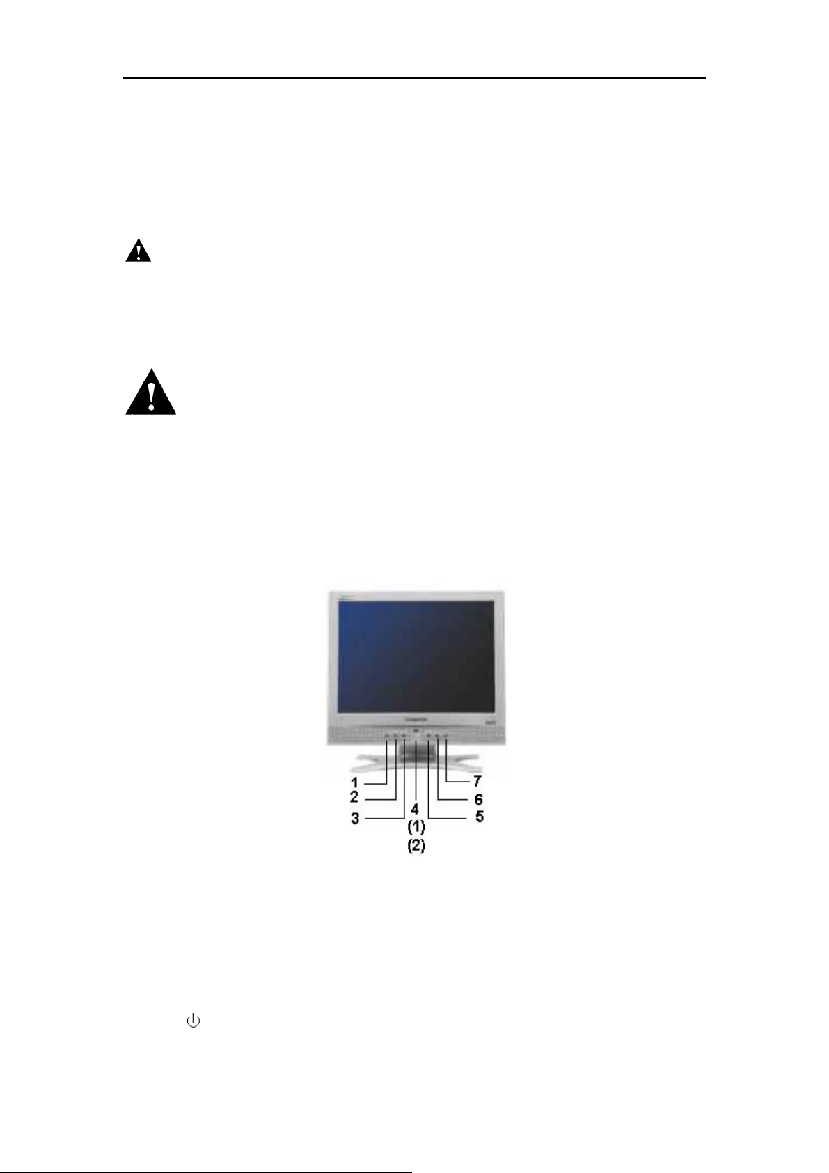
CONTROL BUTTONS
Panel Buttons
Panel Buttons
1
2
3
4
【MENU】
【VOL-】
【VOL+】
【
】
Launches the OSD (On-Screen Display) menu. Scrolls the
OSD menu. Th
remote control.
Decrease the sound volume. Decrease/Switch the valu
the selected item in menu operation.
Increase the sound volume. Increa
selected item in menu operation.
Turn the power on/off. Th
on the remote control.
e function is same to the 【MENU】on the
e of
se/Switch the value of the
is function is same to the 【POWER】
3
Page 5

H-LCD2000Service Manual Page 4 of 57
5
6
7
(1) Remote Sensor Receive the signal from the remote control
(2) Indicator 1. Red Light-indicates Standby/Normal work mode
NOTE: In this operation manual, symbol 【】means Button.
【CH-】
【CH+】
【SOURCE】
1. In TV mode, decrease channel number or select functions
in menu.
2. In PC mode, select functions in menu only.
1. In TV mode, increase channel number or select functions in
menu.
2. In PC mode, select functions in menu only.
Scrolls between TV, S-Video, AV, PC, and YPbPr modes.
The function is same to the【TV/AV】on the remote control.
2. Green light-indicates Standby with a certain preset ON time
3. No light-indicates Power Off
4
Page 6
H-LCD2000Service Manual Page 5 of 57
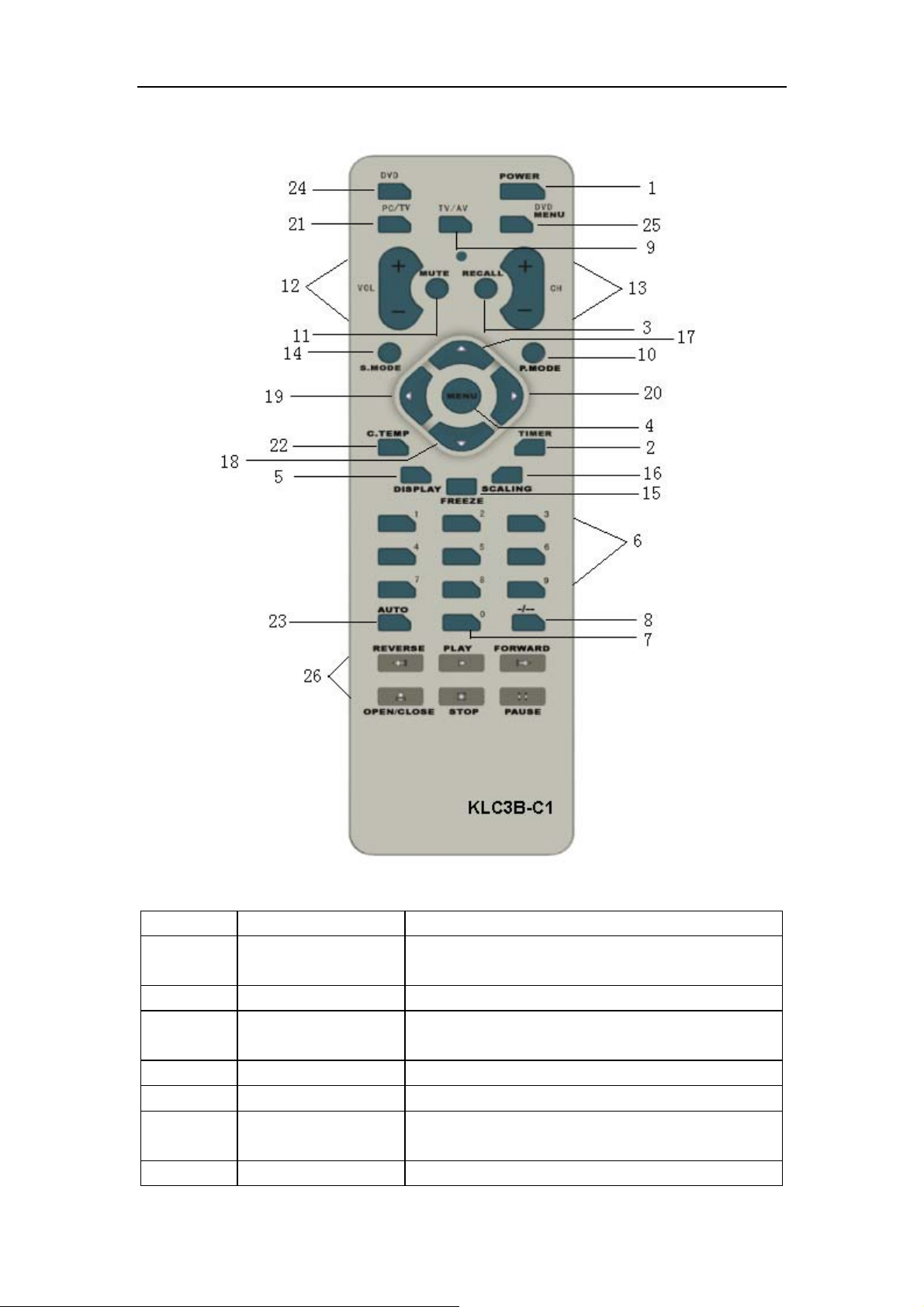
Remote Control Buttons
1
2
3
4
5
6, 7 No. 0-9 Channel select (in TV mode)
8
9
【POWER】
【TIMER】
【RECALL】
【MENU】
【DISPLAY】
【-/--】
【TV/AV】
Turn the LCD TV On or STANDBY
1. Standby the LCD TV in a certain preset time
2. Turn the LCD TV on with a fixed channel
In TV mode, scroll to the previous channel
Press this menu repeatedly to scroll between all
the menus, also press it to exit
To check the current mode
In TV mode, switch the channel number between
one-digit, two-digit and three-digit
Switch between TV, S-Video, AV, PC, YPbPr
5
Page 7
H-LCD2000Service Manual Page 6 of 57
signal sources
10
11
12
13
14
15
16
17, 18
【P.MODE】
【MUTE】
【VOL+】【VOL-】
【CH+】【CH-】
【S. MODE】
【FREEZE】
【SCALING】
【
】/【 】
Switch between User, Soft, Standard and Bright
modes
Turn the MUTE ON/OFF
Increase/Decrease the volume or exit from the
mute mode
1. In TV mode, increase/decrease the channel
number
2. Switch from other signal sources to TV mode
rapidly
Switch between User/Music /standard/ theater
mode orderly
Invalid buttons for this product
Invalid buttons for this product
Select functions in menu
19, 20
21
22
23
24, 25, 26 Remain buttons Invalid buttons for this product
Note:
①When in operation, please point your remote control directly to the infrared sensor.
②Do not expose the remote control to impacts, water or disassemble it.
③Do not repeatedly press the buttons on the remote control. Allow interval of no less than
one second between selections.
I. In TV, S-Video, AV, and YPbPr Modes
General Operation
Standby Mode
Press the【
store the current setup and enter into the standby mode with a black background. When
press the button again, the LCD TV works again.
TV/AV Signal Switch
Press the 【SOURCE】on the panel or the【TV/AV】on the remote control to select the
signal sources orderly. They are TV, S-Video, AV, PC, and YPbPr.
Press【PC】to switch between TV and PC directly.
Channel Switch
【
】/【 】
【PC/TV】
【C.TEMP】
【AUTO】
】on the TV panel or the【POWER】on the Remote Control, the LCD TV will
Adjust the fixed menu items
Switch between TV and PC signal directly
Switch between User, Cool, Neutral and Warm
modes in PC mode
Adjust the picture’s quality automatically in PC
mode
6
Page 8

H-LCD2000Service Manual Page 7 of 57
Press the 【CH+】/【CH-】 to increase or decrease the channel number orderly. For
example, if the current number is in SKIP ON mode, then the program will switch to the
next channel automatically.
You can also input the digit number 0-9 directly.
The channel number is on the upper-right corner of the screen. (See the following chart)
The SKIP OFF channel number is green and the SKIP ON channel number always with a
* symbol behind itself.
Note:
In S-Video, AV, and YPbPr mode, press【CH+】/【CH-】 to watch the program directly.
Channel Selection
In TV mode, press the【-/--】repeatedly to switch the channel numbers between one-digit,
two-digit and three-digit, and the corresponding “-“, ”- -”, ”- - -” symbols will appear on the
upper-right corner of the screen.
1. In “-”mode, any of the ten Arabic numerals 0 to 9 can be selected as the channel
number.
2. In “- -” mode, if the input “2-“ is interrupted by any other operations, channel 2 will be
the default setting.
3. In “- - -” mode, range 0~235 is valid and the input number is invalid if it is out of the
range.
If the first input number is “2 - -”, and there is no any other operations within 5 seconds,
channel 2 will become the default setting. The setup and operation of “21 -” is same to
“2 - -”.
In the modes above, whenever the channel is SKIP ON or OFF, the input channel number
is always valid.
Note:
In S-Video, AV, YPbPr, and PC mode, press any of the ten Arabic numerals 0 to 9 to watch
the corresponding programs.
---
7
Page 9
H-LCD2000Service Manual Page 8 of 57
r
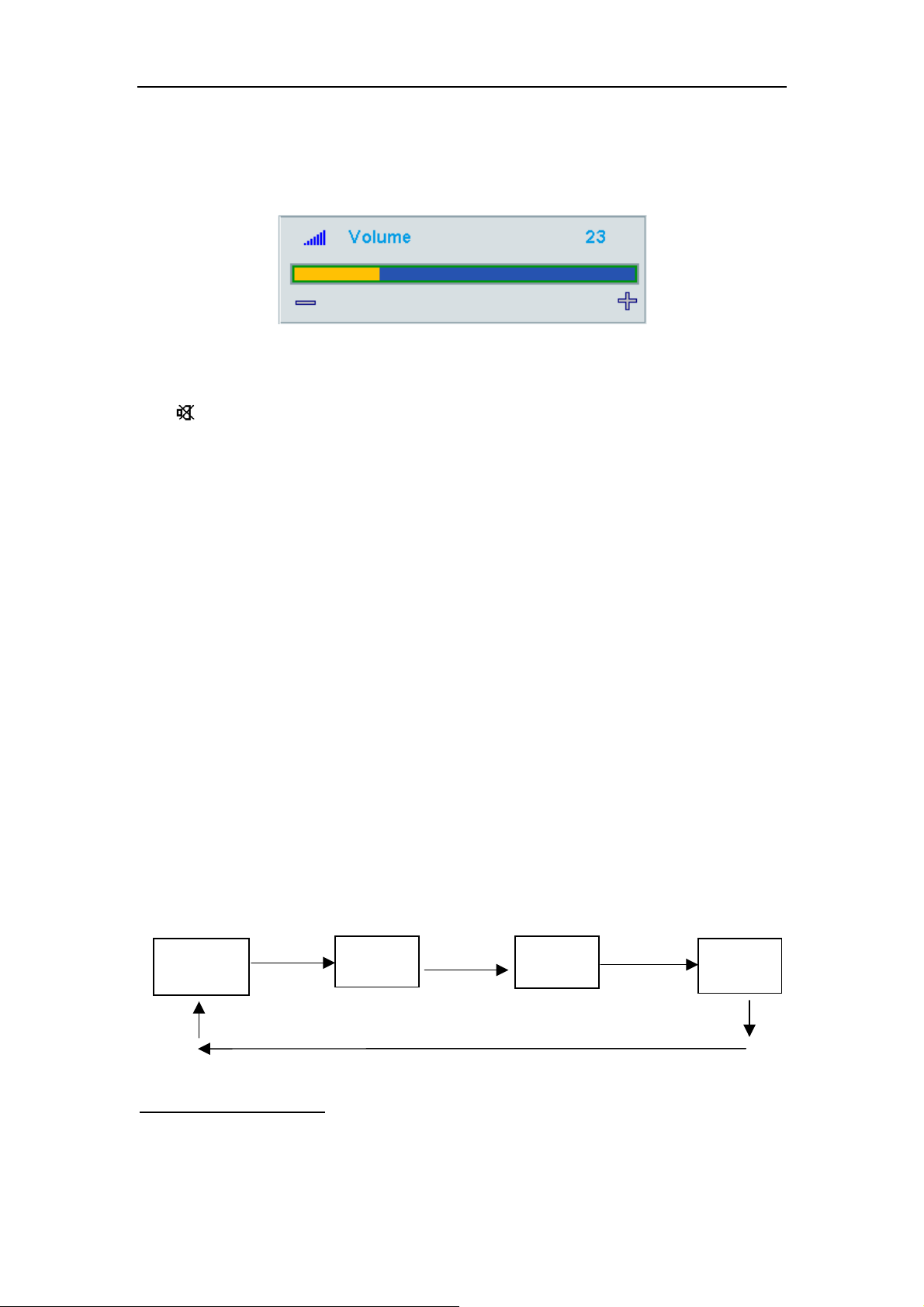
Volume Control
Press the【VOL+】/【VOL-】 to decrease or increase the volume continuous when there
is no any menus displayed on the screen. The range is 0-100.
The Volume menu will exit automatically if there is no operation within 6 seconds.
Mute
Press the【MUTE】on the remote control to turn On/Off the MUTE mode.
The
any operation unless you turn the Mute OFF.
Press the【MUTE】again to turn the Mute off.
Altering the value of volume, treble, bass or balance can also turn the Mute OFF.
When there is no signal and with a blue background on the screen, the TV will mute.
Note:
In S-Video, AV, and YPbPr modes, when there is no signal and with blue background on
the screen, the TV will not mute.
Picture Mode Selection
Press the【P.MODE】to switch between user, soft, standard and bright modes.
The value of Soft, Standard, and Bright are the default setting, and they cannot be
adjusted.
In this function, only the User mode can be adjusted.
Note:
In S-Video, AV mode, the setup and operation are same to the TV mode.
No this function in YPbPr mode.
Information Display
In TV mode, except the searching process, when there is any menu displayed on the
screen, press the【DISPLAY】to turn it off. Press【DISPLAY】again, the CHANNEL
NUMBER, TIMER, SIGNAL SOURCE, OFF DISPLAY modes will appear on the screen
orderly.
symbol always remains on the upper-right corner of the screen whenever you do
Channel
Numbe
Note:
In AV, S-Video, YPbPr modes, there is no channel number display.
Channel Number Display:
Only in TV mode, the current channel number can be displayed on the upper-right corner
of the screen.
Timer
8
Signal
OFF
Page 10
H-LCD2000Service Manual Page 9 of 57
Timer Di splay:
Please refer to the TIMER part to get more details about the Sleep Timer function.
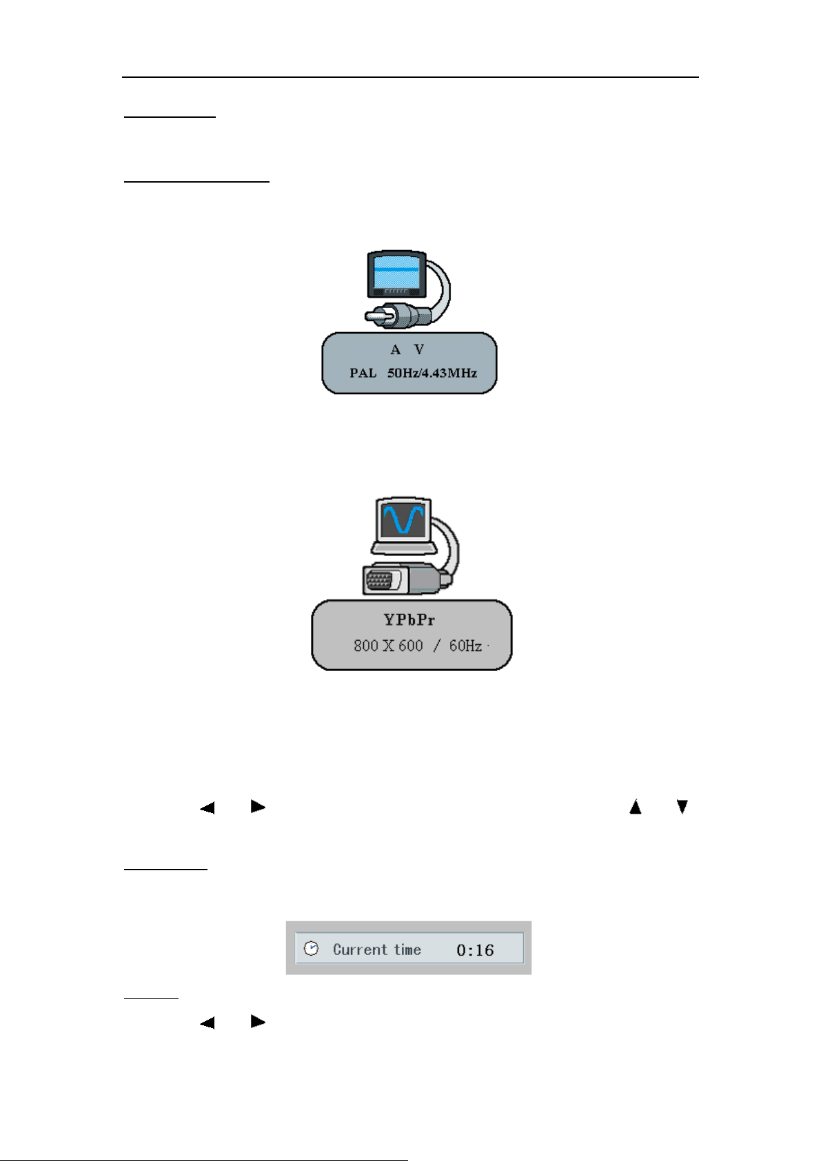
Signal Source Display:
In TV, AV, S-Video modes, the follow illustration will appear on the upper-right corner of
the screen.
In the illustration above, AV is the current signal source; PAL is the current color system.
In YPbPr mode, the resolution and refresh rate of the picture will be displayed on the
screen.
See the follow illustration:
Timer
In TV mode, press the【TIMER】on the remote control, the screen displays the current time
of the TV. When press the button repeatedly, the screen will display the Current Time, On
Time, Channel On, Off Time, and Sleep Timer in turn.
Press it again to exit.
Press the【
to alter the value of HOUR/MINUTE when the digit become blue.
Current Time
If it is the first time you use your LCD TV or you have been turn the power off, the screen
displayed time will automatically back to 00:00.
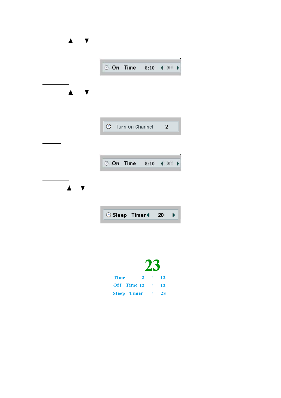
On Time
Press the【
】/【 】to select HOUR/MINUTE of the clock, and press the【 】/【 】
】/【 】to select the HOUR/MINUTE/On Time ON or OFF.
9
Page 11
H-LCD2000Service Manual Page 10 of
57
Press the【 】/【 】to alter the value of your desired item.
Please set OFF if you do not want to turn on the TV automatically.
Channel On
Press the【
For instance, the TV displays channel 2 directly when you turn it on if the preset channel
number is 2.
Off Time
The operation is same to the On Time mode.
Sleep Timer
Press the【
orderly.
Note:
In AV, S-Video, YPbPr modes, the setup and operation of this menu are same to the TV
mode.
In TV mode, the upper-right corner displays the following OSD if the Sleep Timer is on.
】/【 】to select the desired channel number.
】/【 】to select the sleep time among 10, 20, 30, 60, 90, 120, 180, and OFF
Note: No channel number in S-Video, AV, and YPbPr modes.
Recall
In TV mode, press the【RECALL】to view the previous channel.
In AV, S-Video, YPbPr modes, there is no this operation.
10
Page 12
H-LCD2000Service Manual Page 11 of
57
Menus
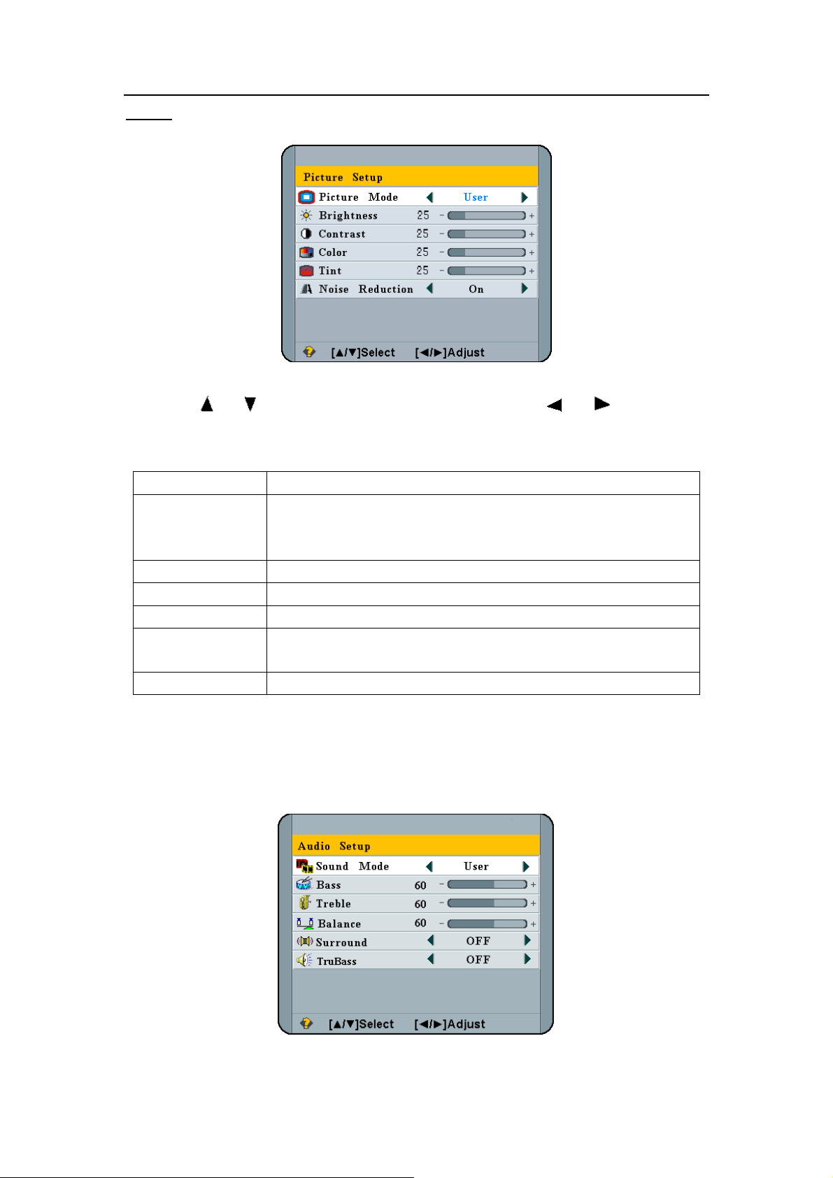
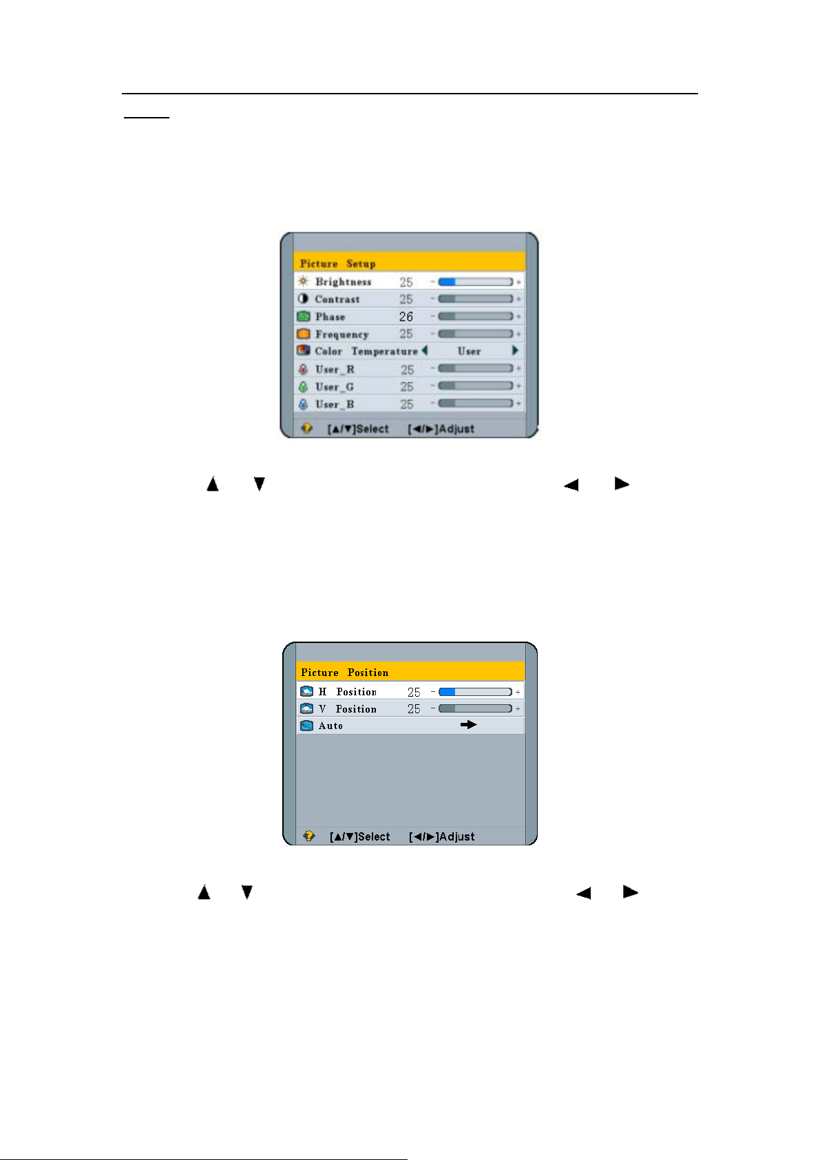
Using the Picture Setup Menu
1) Press【MENU】repeatedly to enter the Picture Setup menu.
2) Press 【
3) Base operation:
Note:
1. In S-Video, AV modes, the setup and operation are same to the TV mode.
2. In YPbPr mode, only Brightness, Contrast and Color can be adjusted.
Using the Audio Setup Menu
】/【 】 to select the desired adjustment; press 【 】/【 】 to make the
desired adjustment.
Option Description
Switch between User, Soft, Standard, and Bright modes orderly.
Mode
Brightness To brighten or darken the picture.
Contrast To increase or decrease the gain of the picture.
Color To increase or decrease the chroma of the picture.
Tint
Noise Reduction Turn On/Off the noise red uce function
Only in user modes, the Brightness, Contrast, Color, Tint modes
can be altered.
To increase or decrease the green tones of the picture. (For
NTSC signal only)
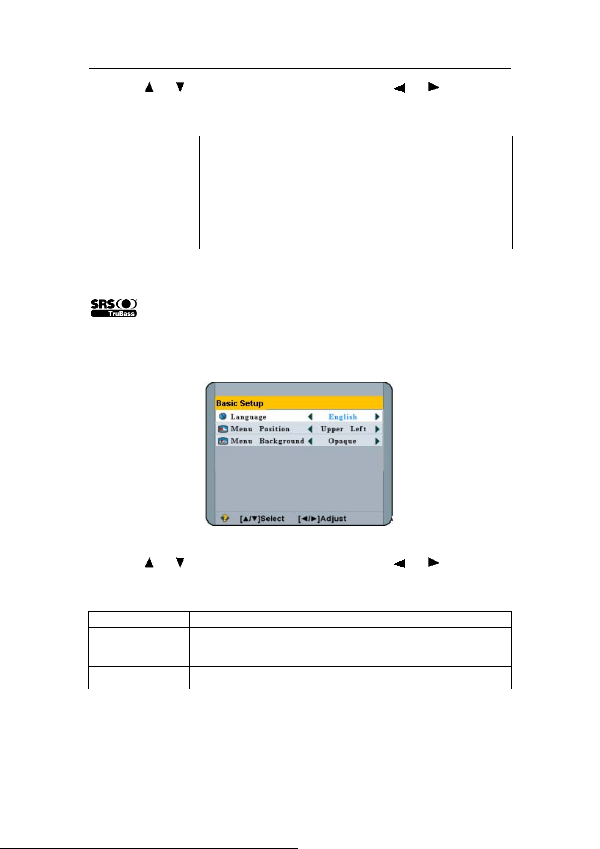
1) Press【MENU】repeatedly to enter the Audio Setup menu.
11
Page 13
H-LCD2000Service Manual Page 12 of
57
2) Press 【 】/【 】 to select the desired adjustment; press 【 】/【 】 to make the
desired adjustment.
3) Basic Operation:
Option Description
Sound Mode Switch between Music, User, Theater, and Standard modes
Bass To increase or decrease lower-pitched sounds
Treble To increase or decrease higher-pitched sounds
Balance To balance the left and right speaker
Surround To turn On/Off the surround function
TruBass To turn On/off the TruBass function
Note:
In S-Video, AV, YPbPr modes, the setup and operation are same to the TV mode.
is a trademark of SRS Labs, Inc. TruBass technology is incorporated under
license from SRS Labs, Inc.
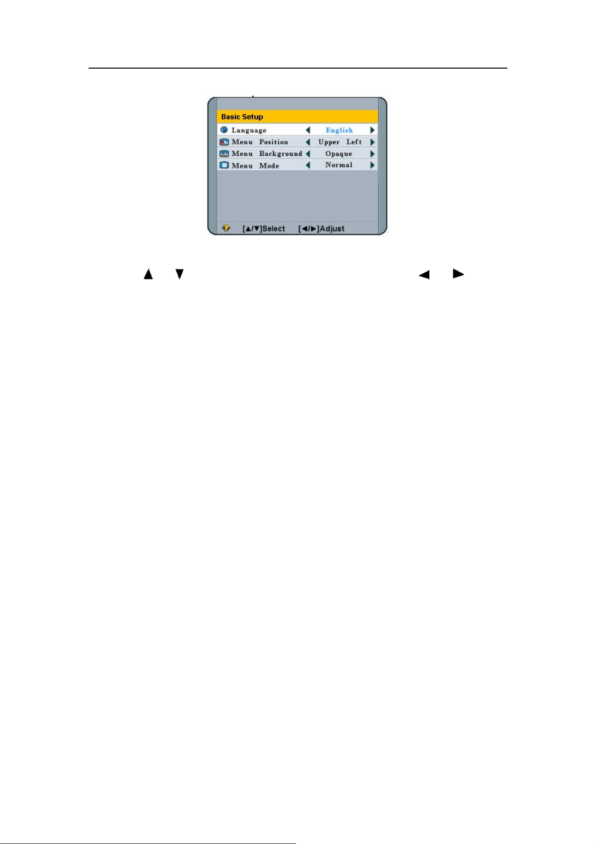
Using the Basic Setup Menu
1) Press【MENU】repeatedly to enter the Basic Setup menu.
2) Press 【
desired adjustment.
3) See the following chart for more details:
Option Description
Language Select Russian or English as the menu language.
Menu Position Adjust Main Menu’s position. (Nine modes for selection.)
Menu Background Select Menu Background between Opaque and translucent.
Note:
In S-Video, AV, YPbPr modes, the setup and operation are same to the TV mode.
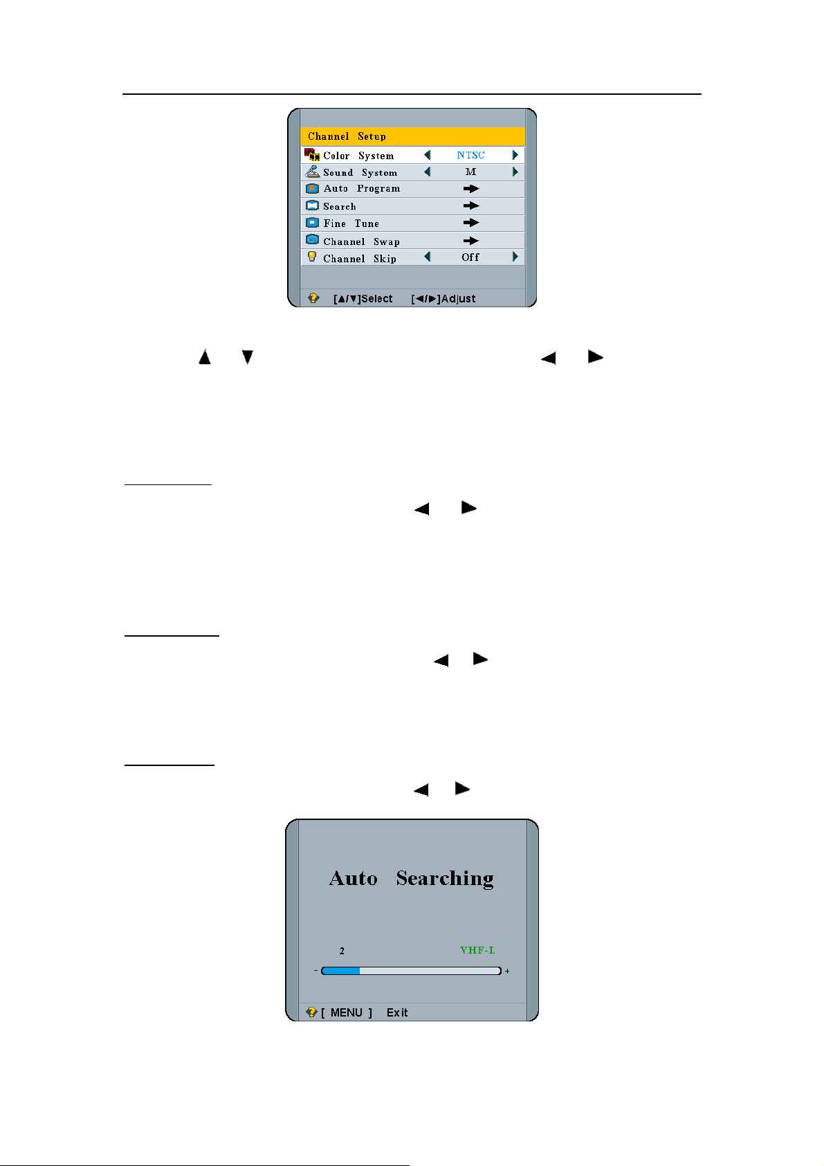
Using the Channel Setup Menu (No this menu in YPbPr mode)
】/【 】 to select the desired adjustment; press 【 】/【 】 to make the
12
Page 14
H-LCD2000Service Manual Page 13 of
57
1) Press【MENU】repeatedly to enter the Channel Setup menu.
2) Press 【
desired adjustment.
3) In AV, S-Video mode, only Color System can be adjusted.
4) In YPbPr mode, there is no channel setup menu.
5) Basic Operation:
Color System
In TV mode, select Color System and press【
NTSC4.43, PAL, PAL60, and SECAM Modes.
Note:
In S-Video, AV modes, the setup and operation are same to the TV mode.
Sound System
1. In TV mode, select Sound System and press【
and I sound systems.
2. Noise appears with wrong selection.
Auto Program
】/【 】 to select the desired adjustment; press 【 】/【 】 to make the
】/【 】to switch between AUTO, NTSC,
】/【 】to Switch between D/K, M, B/G,
In TV mode, select Auto Program and press【
1. Automatically search and store programs from VHFL channel one to UHF.
】/【 】to enter the Auto Searching mode.
13
Page 15
H-LCD2000Service Manual Page 14 of
57
2. During searching, the preset sound system is valid. You can select your desired
sound system to watch the programs smoothly.
3. When searching is finished or the 236 program positions are all occupied, or press
the【MENU】during the searching process, the search will be automatically stopped
and back to the Channel Setup menu with channel one.
4. It always mutes during searching, and no sound output.
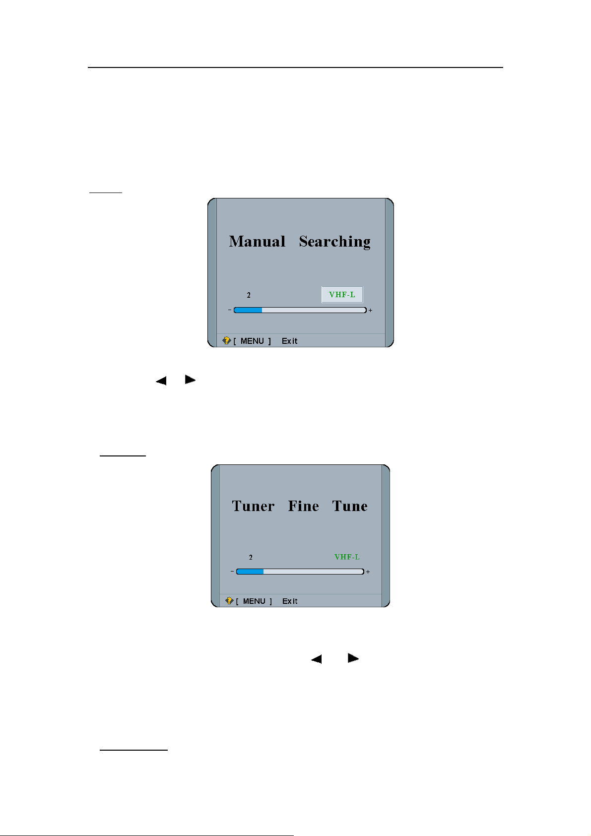
Search
In TV mode, select Search to enter the Manual Searching mode.
Press the 【
After searching, the TV will automatically store receivable channels and return to the
menu.
Fine Tune
When the picture and sound of a channel are not satisfactory after Auto Program or
Search, please use the Fine Tune function.
】/【 】so that the TV searches another lower or upper program position.
1. In TV mode, select Fine Tune and press 【
mode.
2. After searching, the TV will automatically store receivable channels and return to the
menu.
Channel Swap
14
】/【 】to enter the Tuner Fine Tune
Page 16
H-LCD2000Service Manual Page 15 of
57
To exchange any two program’s channel numbers directly in TV mode.
For instance, if CCTV is stored at channel 18 after Auto Searching, you can exchange
CCTV to channel 1 directly.
Channel Skip
After Auto Searching, there may be some repeated programs or interior signal received.
Skipping the undesired program position can dramatically quicken program selection.
1. Select Channel Skip to enter the Channel Skip mode.
2. Press the【
3. Press the【CH+】/【CH-】you will find the position number skipped.
4. Input the channel number directly to resume the position number that has been
skipped.
II. In PC, DVI Modes
General operation
Signal Sources Switch
1. Press【TV/AV】to switch between PC, S-Vedio, YPbPr, TV , and AV signal sources. The
operation is same to the TV mode.
2. Press the【PC】to switch between TV and PC modes directly.
3. Press any of the ten Arabic numerals 0 to 9 to watch these programs.
Volume Control
The operation is same to the TV mode.
Mute
The operation is same to the TV mode.
Information Display
Press the【DISPLAY】to check the signal source. Press it again to exit.
】/【 】to on/off the Channel Skip mode of the current channel.
In the illustration above, PC is the signal source, 800 X 600 is the resolution, and 60Hz is
the refresh rate.
15
Page 17
H-LCD2000Service Manual Page 16 of
57
Menus
Recommended Resolution
The valid resolution of your LCD TV is 800x600, please set it as your computer output
resolution so that you can view your LCD TV more enjoyable.
Picture Setup Menu
In PC mode, press the【MENU】repeatedly to enter the Picture Setup menu.
Press the 【
】/【 】to select the desired adjustment; press the【 】/【 】to make
the desired adjustment.
Only when the Color Temperature is in User Mode, the value of User-R, User-G, and
User-B can be changed. In Cool, Neutral or Warm mode, they are brown and cannot be
changed.
Picture Position Menu
In PC mode, press the【MENU】repeatedly to enter the Picture Position menu.
Press the【
】/【 】to select the desired adjustment, and press the【 】/【 】to alter
the value of the desired adjustment (H-Position, V-Position and Auto) to get a more
comfortable picture view.
Audio Setup Menu
In PC mode, press the【MENU】until the Audio Setup Menu.
The operation is same to the TV mode.
16
Page 18
H-LCD2000Service Manual Page 17 of
57
Basic Setup Menu
In PC mode, press the【MENU】repeatedly to enter the Basic Setup Menu.
Press the【
the value of the desired adjustment.
】/【 】to select the desired adjustment, and press the【 】/【 】to alter
POWER MANAGEMENT
1. In PC mode, in order to save the power energy and prolong your LCD TV’s lamp life,
the LCD TV will automatically power off within 15 seconds and enter into the Power
Energy Saving Mode if there is no VGA signal input.
The LCD TV will automatically exit from the Power Energy Saving Mode and work again
when it received a valid VGA signal.
2. In TV mode, the LCD TV is standby with a black background if there is no signal input or
any operation with 15 minutes.
17
Page 19
H-LCD2000Service Manual Page 18 of
57
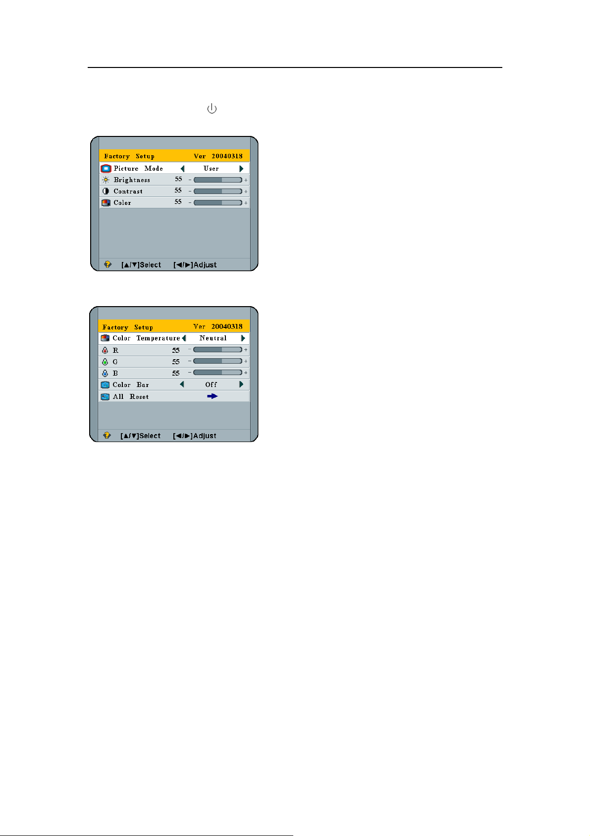
ENTER THE SERVICE MODE
Press【MENU】 and 【 】buttons at the same time to enter into the service mode.
See the following illustration (the picture mode can be adjusted):
Press 【MENU】button again to adjust the items in the following menu:
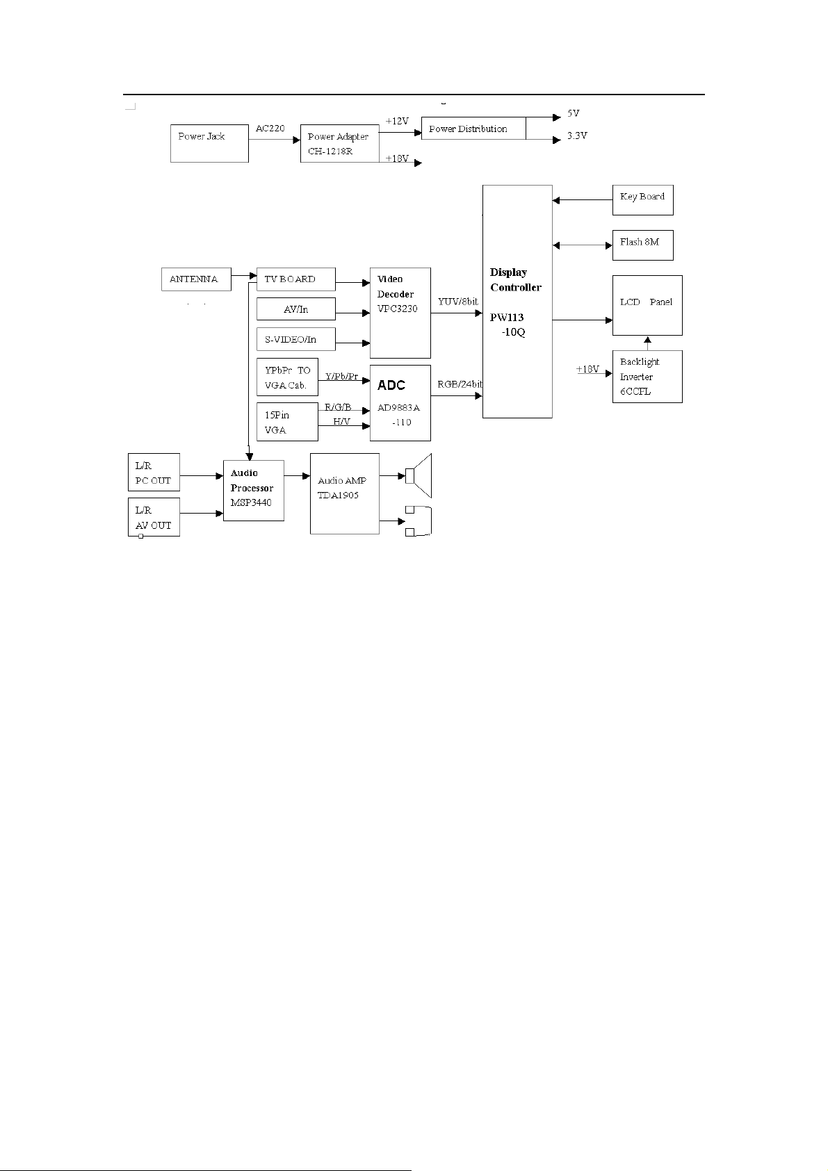
CHASSIS FUNCTION DESCRIPTION
Block Diagram
18
Page 20
H-LCD2000Service Manual Page 19 of
57
19
Page 21
H-LCD2000Service Manual Page 20 of
57
Chassis Description
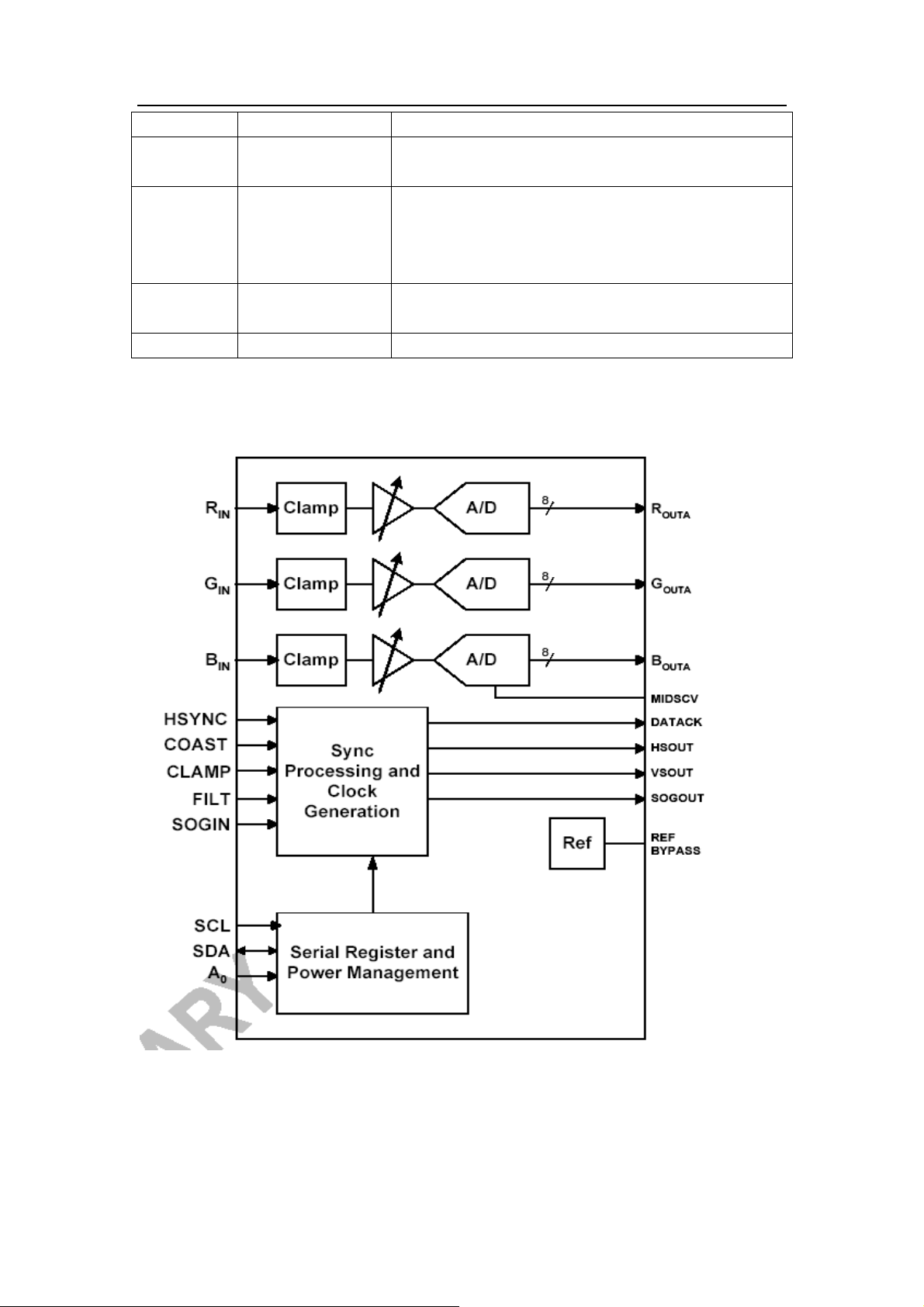
AD9883A
AD9883A omplete 8-bit, onolithic analog interface optimized for
The is a c 140 MSPS m
capturing RGB graphics signals from
encode rate c
up to SXGA (1
AD9883A’s on-chip PLL generates a pixel clock from HSYNC and COAST inputs.
The
Pixel clock ou put fr
a and full powe 300 MHz supports resolutions
pability
280 ×
t equencies range from 20 MHz to 140 MHz.
1024 at 75 Hz).
personal computers and workstations. Its 140 MSPS
r analog bandwidth of
Features
140 MSPS Maximum Conversion Rate
300 MHz Analog Bandwidth
0.5 V to 1.0 V Analog In
500ps p-p PLL Clock Jitter at 110 MSPS
Low Power Supply
Full Sync Processing
Sync Detect for ”Hot Plugging”
Midscale Clamping
Power
Low Power: 500 mW Typical
4:2:2 Output Format Mode
AD9883A
Pin Name Function
70~ RED0~RED7
2~9
12~19 BLUE0~BLUE7
67 DATACK Data Output Clock
66 HSOUT HSYNC Output (Phase-Aligned with DATACK)
65 SOGOUT Sync on Green Slicer Output
64 VSOUT VSYNC Output (Phase-Aligned with DA TACK)
37 MIDSCV Internal Midscale Voltage Bypass
58 BYP Internal Reference Bypass REF
31 VSYNC Vertical SYNC Input
30 HSYNC Horizontal SYNC Input
43 BAIN Analog Input for Converter B
49 SOGIN Input for Sync-on-Green
48 GAIN Analog Input for Converter G
54 RAIN Analog Input for Converter R
29 COAST PLL COAST Signal Input
38 CLAMP Clamp Input (External CLAMP Signal)
55 A0 Serial Port Address Input 1
56 SCL Serial Port Data Clock (100 kHz Maximum)
-Down Mode
Pin Function
77
put Range
GREEN0 ~
GREEN7
Outputs of Converter “Red,” Bit 7 is the MSB
Outputs of Converter “Green Bit 7 is the MSB
Outputs of Converter “Blue,” Bit 7 is the MSB
20
Page 22
H-LCD2000Service Manual Page 21 of
57
57 SDA Serial Port Data I/O
33 FILT
26,27,39
42,45,46
51,52,59
62
11,22,23,
,78,7969
34,35
Block Diagram for AD9883A
,
,
,
D AVD
V33 Output Power Supply
PVDD PLL Power Supply
Connection for External Filter Components for
Internal PLL
Analog Power Supply
21
Page 23
H-LCD2000Service Manual Page 22 of
57
VPC3230
VPC 32 4xD is a high-q -chip video front-end, which is targeted for
The 3xD/32 uality, single
and 16:9 and 100/120 H
4:3 , 50/60 z TV sets.
tures
Fea
High-pe e adaptive 4 eparator with adjustable vertical
rformanc H comb filter Y/C s
peaking
Multi-standard color decoder PAL/NTSC/SECAM including all sub standards
Four CVBS, one S-VHS input, one CVBS output
Two RGB/YCrCb component inputs, one Fast Blank (FB) input
Integrated high-quality A/D converters and associated clamp and AGC circuits
Multi-standard sync processing
Linear horizontal scaling (1/4 ~4), as well as non-linear horizontal scaling ‘panorama
vision’
Peaking, contrast, brightness, color saturation and tint for RGB/YCrCb and
CVBS/S-VHS
Display and deflection control (VPC 324xD)
High-quality soft mixer controlled by Fast Blank
PIP processing for four
picture sizes (1/4,1/9,1/16,1/32of normal size)
15 predefined PIP display configurations and expert mode (fully programmable)
Control interface for external field memory
2
I
C-Bus Interface
One 20.25 MHz crystal, few external components
Pin Function
Pin Name Function
1~3
4~6
R1G1B1IN Analog Component Input 1
R2G2B2IN Analog Component Input 2
7,64,30,
11 , 12,
25, 35,
65, 77,
GND Analog Shield GNDF
46, 51,
68,80
8 NC Not connected
9 VSUPCAP Supply Voltage, Digital Decoupling Circuitry
10, 29,
36, 45,
2
5
59, 69,
76
V33 Supply Voltage, Digital Circuitry
AVCC Supply Voltage
13 SCL I2C Bus Clock
14 SDA I2C Bus Data
15 RESQ Reset Input, Active Low
22
Page 24
H-LCD2000Service Manual Page 23 of
57
16 TEST Test Pin, connect to GNDD
17 VGAV VGAV Input
18 YCOEQ Y/C Output Enable Input, Active Low
19~23
FFIE Not connected
24 CLK20 Main Clock Output 20.25 MHz
27 LLC2 Double Clock Output
28 LLC1 Not connected
31~34
37~40
41~44
47~50
Y0~Y7
C0~C7
Picture Bus Luma
Picture Bus Chroma
53 INTLC Interlace Output (0-odd field, 1-even field)
54 AVO Active Video Output
55 FSY/HC Not connected
56 MSY/HS Main Sync/Horizontal Sync Pulse
57 VS Vertical Sync Pulse
58 FPDAT Not connected
60 CLK5 CCU 5 MHz Clock Output
61 NC Not connected
62 XTAL1 20.25M Analog Crystal Input
63 XTAL2 20.25M Analog Crystal Output
66 VRT Reference Voltage Top, Analog
67 I CSEL
2
I2C Bus Address Select
70 VOUT Analog CVBS Output
71 CIN S-Video Chroma Input
72 VIN1 S-Video Luma Input
73 VIN2 Video Input
74 VIN3 TV CVBS Input
78 VREF
Reference Voltage Top, Analog Component
Inputs Front-End
79 FB1IN Fast Blank Input
23
Page 25

H-LCD2000Service Manual Page 24 of
57
Block Diagram 3230
for VPC
PW113
The PW113 essor is ” solution, optimized for
high-perform value-line flat panel mon
In addition, the PW113 high-performance,
ammable rizontal and ve
progr , ho rtical image scalars with intelligent Auto Image
Optimization circuitry to deliver crisp on the screen.
tent-pend ail-Safe™ mode
A pa ing F provides full VESA Plug-’n-Play compatibility without
requiring a frame buffer. The Im r also couples second-generation,
performance, programmable h
high- orizontal and vertical image scalars with intelligent
Image Proc a “system on a chip
ance yet cost sensitive, itors.
Image Processor couples second generation,
, perfect images
age Processo
Auto Image Optimization circuitry.
puter ima VGA to UX
Com ges from GA (1600x1200) can be resized to fit on a target
display device with any resolution up to SXGA (1280x1024).
mage Pro r supports NTS
The I cesso C or PAL video data with a 4:3 aspect ratio and 16:9
ct ratio so , such as DVD o an be in either YUV4:
aspe urces r HDTV. Video Input formats c
4 bit) or : 2:2 (16 bit) inp integrated ITR656 interface
4:4 (2 YUV4 ut modes. In addition, an
allows 8-bit Y
The PW113 u
g, and also includes two PWM outputs for low-cost backlight or audio control.
timin
An integrat OSD cont orts sophisticated bit-mapped based OSDs
colors from a 64K color pa arent, translucent, and
in/ fade-out functions.
fade-
-chip mic or, with ava reference source code, allows manufacturers to
An on roprocess ilable
lop featur ucts with ra .
deve e-rich prod pid time to market
UV4: 2:2 inputs to interface with many popular video decoders.
s rated PLL to the input
es an integ to synchronize the display interface timing
ed roller supp with 16
lette. The OSD controller supports transp
24
Page 26

H-LCD2000Service Manual Page 25 of
57
Features
ITU-R 656 Video Interface
EMI Reduction Technologies
Real time operation system
Two PWM
Outputs
Patent Pending Fail-Safe
Integrated
PLLs
Intelligent input sign
identify the al mode
Capable to switch the color temperature between YPbPr/YcbCr/YUV-TO-RGB
Sup e Two-pixe technology
ration
Pixel Rate Conversion
M ion Non Scaling
V cessing
Pin Function
71 VCLK VPort Pixel Clock.
74 VVS VPort Vertical Sync.
75 VHS VPort Horizontal Sync.
69 VFIELD Video or Graphics port odd/even field indicator
70 VPEN VPort Pixel Enable.
47~56 YUV0~YUV7
31 GCLK GPort Pixel Clock.
32 GVS GPort Vertical Sync.
33 GHSSOG c-on-Green. GPort Horizontal Sync/GPort Syn
34 GPEN GPort Pixel Enable.
35 GFBK device input Feedback output of an ADC/PLL
20~27 GRE0~GRE7
10~15,18,19 GGE0~GGE7
2~9 GBE0~GBE7
129~136 DGR0~DGR7
119 ~ 122 ,
25~128
1
111~118 DGB0~DGB7
106 DCLK DPort Pixel Clock.
port th l drive LCD
2nd Gene Horizontal and Vertical Image Scaling
Automatic Image Optimization
ulti-Reg -Linear
ideo Pro
dvanced
On-Chip 801
Build-in Pow n Reset circuit
Pin
D Support A OS
86 Microprocessor
er-o
Name Function
Video ns Port Pin Descriptio
VGPort ITUR656 Pixel Data.
Graphics Port Pin Descriptions
GPort Red Pixel Data.
GPort Green Pixel Data.
GPort Blue Pixel Data.
Not connected
DGG0~DGG7
Display Port Pin Descriptions
Not connected
Not connected
25
Page 27

H-LCD2000Service Manual Page 26 of
57
108 DVS DPort Vertical Sync.
109 DHS DPort Vertical Sync.
110 DEN DPort Pixel Enable.
96~103 DR0~DR7
88~95 DR0~DR7
76~83 DB0~DB7
Microprocessor Interface Pin Descriptions
194 WR
195 RD
196 ROMOE
197 ROMWE
198 CS0 Miscellaneous Chip Select 0.
199 CS1 Miscellaneous Chip Select 1.
193 NMI Non-maskable Interrupt.
1641,173~
84,187~ A1~A19
192
148~163 D0~D15
Peripheral Interface Pin Descriptions
207 PORTA0 SDA
206 PORTA1 SCL
204 PORTA3 STANDBYsignal
203 PORTA4 Ir signal input
57 PORTB0 Swo
58 PORTB1 Sw1
60 PORTB3 DVI sel
61 PORTB4 LVDS enable
62 PORTB5 YC enable
63 PORTB6 Black light on
64 PORTB7 LCD enable
39~45
67 RXD Serial Receive Data.
68 TXD Serial Transmit Data.
142 TEST Test mode enables.
139 RESET Bi-directional reset pin.
169 XI Crystal input.
170 XO Crystal input.
PORTC0 ~
PORTC7
Miscellaneous Pin Descriptions
DPort Red Pixel Data.
DPort Green Pixel Data.
DPort Blue Pixel Data.
Write Enable low indicates a write to external RAM or
other devices.
Read Enable low indicates a read to external RAM or
other devices.
ROM Output Enable low output indicates a read from
external ROM.
ROM Write Enable low indicates a write to external
ROM.
Microprocessor address bus output bits
Microprocessor 16-bit bidirectional data bus
Panel button input
26
Page 28

H-LCD2000Service Manual Page 27 of
57
Power supply & GND
1
6,37,65,
84
,137,185
17,38,66,
85,138,186
29,52,72,
86 , 104 ,
123,140,
171,208
1,30,53,
73,87,105,
124,141,
172
165 VDDPA2 1.8V analog clock generator power.
166 VSSPA2 Clock generator analog ground.
167 VDDPA1 1.8V analog clock generator power.
168 VSSPA1 Clock generator analog ground.
VDD1
VSS Digital core ground.
VDDQ3
VSSQ Digital I/O groun
1.8V digital core power.
3.3V digital I/O power.
d.
27
Page 29

H-LCD2000Service Manual Page 28 of
57
Block Diagram for PW113
28
Page 30

H-LCD2000Service Manual Page 29 of
57
MSP3440
MSP 34x0G family of sing tandard covers the sound
The le-chip Multis Sound Processors
essing of all analog TV-St ide, a
proc andards worldw s well as the NICAM digital sound
standards. Th rocessing, ith analog sound
processed rformed o chip.
he MSP 34x0G has built-in automatic functions: The IC is able to detect the actual sound
T
tandard automatically (Automatic Standard Detection). Furthermore, pilot levels and
s
identificatio
stereo/bilingual; no I
e full TV sound p starting w IF signal-in, down to
analog AF-out, is pe n a single
n signals can be evaluated internally with subsequent switching between mono/
2C interaction is necessary (Automatic Sound Selection).
Features Summary
1、Sound IF Proce
ssing
2、Preprocessing for SCART and I2S Input Si
3、Source Selection
and Output Channel Matrix
4、Audio Baseband Processing
5、SCART Signal Routing
6、I2S Bus Interface
、ADR Bus Interface
7
8、Digital Contro
lock PLL Crys ications
9、C Oscillator and tal Specif
l I/O Pins and Status Change Indication
e diagram MSP3440
Th of
gnals
29
Page 31

H-LCD2000Service Manual Page 30 of
57
Pin Function
Pin FunctName ion
1,18,19,20,22,23,29,31,3
41,42,46,59,63,64,75,76
9
2,
NC
ADR_WS ADR word e strob
Not Connect
8 ADR_DA ADR data ut outp
7 NC I2S_DA_IN1
6
5
4
3
2
I2S_DA_OUT I2S data output
I2S_WS I2S word strobe
I2S_CL I2S clock
I2S_DA I2S data
I2S_CL I2S clock
I2S1 data input
80 STANDBYQ Stand-by( ctive) low-a
79 ADR_SEL I2C Bus address select
78 D_CTR_I/O_0 D_CTR_I/O_0
77 D_CTR_I/O_1 D_CTR_I/O_1
74 AUD_CL_OUT Audio clock output(18.432MHz)
73 TP Test pin
72 XTAL_OUT Crystal oscillator
71 XTAL_OUT Crystal oscillator
70 TESTIN Test pin
69 ANA_IN2+
68 ANA_IN-
IF input2(can be left vacant, only if
input1 is a ot in use) lso n
IF common be left vacant, only if IF input
1 is also not e)
(can
in us
67 ANA_IN1+ IF input 1
66,6 AVSUP Analog pow supply 5V 5 er
62,61 AVSS Analog ground
60 MONO_IN Mono input
58 VERFTOP Reference voltage IF A/D converter
57 SC1_IN_R SCART 1 input, right
56 SC1_IN_L SCART 1 input, left
55,52,49 ASG Analog Shi Ground eld
54 SC2_IN_R
66 SC2_IN_L
51 SC3_IN_R
50 SC3_IN_L
48 SC4_IN_R
47 SC4_IN_L
SCART 2 in put, right
SCART 2 input, left
SCART 3 in put, right
SCART 3 input, left
SCART 4 in t, right pu
SCART 4 input, left
45 AGNDC Analog ref ce voltage eren
44,4 AHVSS Analog ground 3
40 CAPL_M Volume capacitor MAIN
39 AHVSUP Analog pow supply 8 V er
30
Page 32

H-LCD2000Service Manual Page 31 of
57
38 CAPL_A Volume capacitor AUX
37
36
SC1_OUT_L SCART ou 1, left tput
SC1_OUT_R SCART ou 1, right tput
35 VREF1 Reference und 1 gro
34
33
SC2_OUT_L SCART ou , left tput 2
SC2_OUT_R SCART outp ut 2, right
30 DACM_SUB Subwoofer output
28 DACM_L Loudspeak ut, left er o
27 DACM_R Loudspeak ut, right er o
26 VREF2 Reference und gro
25 DACA_L Headphone t, left ou
24 DACA_R Headphone , right out
21 RESETQ Power-on-reset
17 I2S_DA_IN2
I2S2-data in put
16,15,14 DVSS Digital ground
13,1 DVSUP Digital pow upply 5 V 2,11 er s
10 ADR_CL ADR clock
TDA 5190
The TDA1905 is a monolithic integrated circuit in POWERDIP package, intended for use as
low f cy power range of applications in io and TV sets.
requen amplifier in a wide rad
Features
ing facility
Mut
ection again ip over temperature
Prot st ch
low noise
Very
supply voltage rejection
High
”switch-on”
Low noise
age range 4V to 30V
Volt
Pin’s nction
Fu
Pin Pin’s Function
Name
1 OUTPUT Audio output
2 VS Power supply
3 BOOTSTRAP Increase of the distortion at low frequency.
4 THRESHOLD Noise reduction
5 MUTING Mute controller
6 INVER Invert input T.IN
7 SVR Supply voltage rejection
8 INPUT Sync. Input
9~16
GND Ground
31
Page 33

H-LCD2000Service Manual Page 32 of
57
Block Diag or Tda1905 ram f
SERVICE DATA
AD9883A)(U3(In V ode):
PIN
NO.
1 0 ∞
2 0.14 ∞
3 2.38 ∞
4 2.44 0 .41
5 2.44 0 .41
6 2.44 0 .41
7 3.0 0
8 3.26 ∞
9 1.22 0 .44
10 0 0 .44
11 3.29 0
12 0.12 0
PIN Voltage
GA M
(V)
GDM8145 multimete
Resistance to Ground
(20KΩ Ran lack probe on GND)
r
ge, B
32
Page 34

H-LCD2000Service Manual Page 33 of
57
13 2.37 3 .73
14 2.45 3 .72
15 2.43 3 .74
16 1.26 0
17 2.39 0
18 2.44 ∞
19 1.98 ∞
20 0 ∞
21 0 ∞
22 3.29 ∞
23 3.29 ∞
24 0 ∞
25 0 0
26 3.31 0 .45
27 3.31 ∞
28 0 ∞
29 0.05 0 .45
30 0.24 0
31 0.01 ∞
32 0 ∞
33 1.54 ∞
34 3.31 ∞
35 3.31 0
36 0 0 .44
37 0.37 ∞
38 0 ∞
39 3.31 ∞
40 0 ∞
41 0 ∞
42 3.31 ∞
43 0.27 ∞
44 0 ∞
45 3.31 0 .44
46 3.31 0
47 0 ∞
48 0.27 ∞
49 0.57 ∞
50 0 ∞
51 3.31 0
52 3.31 0.44
53 0 ∞
54 0.03 ∞
55 0 ∞
33
Page 35

H-LCD2000Service Manual Page 34 of
57
56 3.29 ∞
57 3.29 ∞
58 1.26 ∞
59 3.31 14 .12
60 0 ∞
61 0 ∞
62 3.31 ∞
63 0 ∞
64 0.01 0
65 0.24 0
66 0.08 0.67
67 1.64 0.41
68 0 0
69 3.29 1 4.15
70 0.12 ∞
71 0.04 ∞
72 0.12 ∞
73 0.11 ∞
74 0.11 ∞
75 3.2 ∞
76 0.33 1 4.15
77 3.05 0
78 3.29 0.41
79 3.29 0
80 0 ∞
VPC3230 15
PIN
NO.
)(
U
(
In TV ode):
GDM8145 multimete Mr
PIN Vo
1 1.56 ∞
2 1.42 ∞
3 1.53 变) (跳 ∞
4 2 0.53 .41
5 2 0.53 .41
6 2 0.53 .41
7 0 0
8 0 ∞
9 3 0.29 .63
10 3.29 0.64
11 0 0
12 0 0
13 3.29 3.93
ltage (V)
(20KΩ Range, Black probe on GND)
Resistance to Ground
34
Page 36

H-LCD2000Service Manual Page 35 of
57
14 3.09 3.93
15 3.29 3.94
16 0 0
17 0 0
18 0 ∞
19 2 .57 ∞
20 2.57 ∞
21 0.01 ∞
22 0 ∞
23 0 ∞
24 1.63 ∞
25 0.03 0.01
26 3 0 .25 .65
27 4.6 ∞
28 1.61 ∞
29 3.29 0.63
30 0 0
31 1 .99 ∞
32 0 .82 ∞
33 0 .83 ∞
34 1.08 ∞
35 0 0
36 3.29 0.63
37 1.13 ∞
38 1.08 ∞
39 1 .13 ∞
40 1.24 ∞
41 0 ∞
42 0 ∞
43 0 ∞
44 0 ∞
45 3.28 ∞
46 0 0
47 0 ∞
48 0 ∞
49 0 ∞
50 0 ∞
51 0 ∞
52 3.29 ∞
53 1.65 ∞
54 2 .57 ∞
55 0.1 ∞
56 0 .12 ∞
35
Page 37

H-LCD2000Service Manual Page 36 of
57
57 0.05 ∞
58 3 .28 ∞
59 5.05 ∞
60 2 .45 ∞
61 0 ∞
62 2.27 ∞
63 2.36 ∞
64 0 0
65 0 0
66 0 0.66
67 2.53 0.42
68 0 0
69 5.05 1 2.69
70 1.62 ∞
71 1.37 ∞
72 1.51 ∞
73 1.37 ∞
74 1.49 ∞
75 1.43 ∞
76 5 ∞
77 0 ∞
78 2 0 .53 .41
79 0 ∞
80 0 0
PW113
( )
PIN
NO.
:U18
GDM8145 multimeter
PIN V e (V)
oltag
1 0 0
2 0 ∞
3 0 ∞
4 0 ∞
5 0 ∞
6 0 ∞
7 0 ∞
8 0 ∞
9 0 ∞
10 0 ∞
11 0 ∞
12 0 ∞
(20KΩ Range, Black probe on GND)
Resistance to Ground
36
Page 38

H-LCD2000Service Manual Page 37 of
57
13 0 ∞
14 0 ∞
15 0 ∞
16 1.79 0.42
17 0 ∞
18 0 ∞
19 0 ∞
20 0 ∞
21 0 ∞
22 0 ∞
23 0 ∞
24 0 ∞
25 0 ∞
26 0 ∞
27 0 ∞
28 3 0 .29 .64
29 3 0.29 .64
30 0 0
31 0 ∞
32 0 ∞
33 0 ∞
34 0 ∞
35 0 ∞
36 0 ∞
37 1.79 0.42
38 0 0
39 2.74 1 0.63
40 2.73 1 0.67
41 2.73 1 0.71
42 2.74 1 0.56
43 2.74 1 0.68
44 2.75 1 0.53
45 2.74 1 0.61
46 0 ∞
47 1.28 ∞
48 1.17 ∞
49 1.09 ∞
50 1.13 ∞
51 1.28 ∞
52 3 0 .29 .64
53 0 0
54 0 .89 ∞
55 1.01 ∞
37
Page 39

H-LCD2000Service Manual Page 38 of
57
56 1.49 ∞
57 0 ∞
58 0 ∞
59 0 ∞
60 0 ∞
61 3.29 ∞
62 0 ∞
63 3.29 ∞
64 3.28 ∞
65 1.79 ∞
66 0 0
67 0.98 17.0
68 3.29 ∞
69 1.65 ∞
70 0 ∞
71 1.70 ∞
72 3 0 .29 .46
73 0 0
74 0.06 ∞
75 0.12 ∞
76 1.18 ∞
77 1 .13 ∞
78 0.61 ∞
79 0 .77 ∞
80 1 .32 ∞
81 0 ∞
82 1.57 ∞
83 0 ∞
84 1.79 ∞
85 0 0
86 3.29 0.46
87 0 0
88 1.29 ∞
89 1.25 ∞
90 0.26 ∞
91 0.45 ∞
92 1.26 ∞
93 1.43 ∞
94 1 .42 ∞
95 1.44 ∞
96 1.31 ∞
97 1.18 ∞
98 0.45 ∞
38
Page 40

H-LCD2000Service Manual Page 39 of
57
99 0.42 ∞
100 1.14 ∞
101 1.36 ∞
1 1 02 .44 ∞
1 1 03 .45 ∞
1 004 3.29 .46
1 05 0 0
1 06 1.07 ∞
1 07 1.69 ∞
1 3 08 .28 ∞
1 09 3.28 ∞
1 10 2.72 ∞
111 1.18 ∞
112 1.09 ∞
113 0 .64 ∞
114 0.78 ∞
115 1.39 ∞
116 1.40 ∞
117 1.57 ∞
118 1.62 ∞
119 1.29 ∞
120 1.25 ∞
121 0.25 ∞
122 0.44 ∞
1 3 023 .29 .46
1 24 0 0
1 1 25 .24 ∞
1 26 0 ∞
1 1 27 .34 ∞
1 28 1.45 ∞
1 29 1.31 ∞
1 30 1.08 ∞
1 31 0.44 ∞
132 0.40 ∞
133 1.08 ∞
134 1.35 ∞
135 1.45 ∞
136 1.49 ∞
137 1.80 0.42
138 0 0
139 3.2 3.79 6
140 3.2 0.49 6
141 0 0
39
Page 41

H-LCD2000Service Manual Page 40 of
57
142 0 0
143 0 ∞
144 0 ∞
145 0 ∞
146 0 ∞
147 0 ∞
148 1.05 ∞
149 1.24 ∞
150 1.01 ∞
151 1.16 ∞
152 1.17 ∞
153 1.59 ∞
154 1.69 ∞
155 1.58 ∞
156 1.10 ∞
157 1.45 ∞
158 1.25 ∞
159 1.30 ∞
160 1.56 ∞
161 1.96 ∞
162 1.63 ∞
163 1.79 ∞
164 1.86 ∞
165 1.79 0.42
166 0 0
167 1.79 0.47
168 0 0
169 1.55 ∞
170 1.65 ∞
171 3.29 0.44
172 0 0
173 0.25(changing) ∞
174 0.21(changing) ∞
17 1.74 5 ∞
17 changing) 6 0.17( ∞
17 changing) 7 0.30( ∞
17 1.36 8 ∞
17 0.66 9 ∞
18 2.17 0 ∞
18 0.32 1 ∞
18 2.27 2 ∞
18 changing) 3 0.63( ∞
18 1.49 4 ∞
40
Page 42

H-LCD2000Service Manual Page 41 of
57
18 1.79 5 0.42
18 0 6 0
18 2.59 7 ∞
18 1.97 8 ∞
18 1.58 9 ∞
19 1.17 0 ∞
19 0 1 ∞
19 1.44 2 ∞
19 0 3 3.4
19 0 4 ∞
19 3.29 5 ∞
19 2.31 6 ∞
19 3.29 7 ∞
19 3.29 8 ∞
19 3.29 9 ∞
20 0.06 0 ∞
20 changing) 1 0.21( ∞
20 2.35 2 ∞
20 4.98 3 12.08
20 3.28 4 ∞
20 2.47 5 ∞
20 3.10 6 ∞
20 3.14 7 3.73
20 0 8 0.44
74LVC126A(U11A)(In VGA Mode):
PI
N
NO
.
1 0 8.58
2 0 ∞
3 0.08 ∞
4 3.29 8.58
5 0.25 ∞
6 0.24 ∞
7 0 0
8 0.24 ∞
9 0.24 ∞
10 3.29 8.58
11 .01 0 ∞
12 0 ∞
PIN V
oltage (V)
GDM8145 multimeter
Resis
(20KΩ Range, Black probe on GND)
41
tance to Ground
Page 43

H-LCD2000Service Manual Page 42 of
57
13 3.29 ∞
14 3.29 0.44
TMI1-C13)0I2-2W(A001
PI
N
NO
.
1 32 ∞
2 5.0 3.41
3 0 0
4 3.3 ∞
5 0 ∞
6 4.7 10.0
7 4.5 10.3
8 1.1 ∞
9 1.5 1.06
10 5.0 3.41
1 2.1 1 15.42
PIN V
oltage (V)
(
In TV ode
M
GDM8145 multim
(20KΩ Range, Black probe on GND)
):
eter
Resis
tance to Ground
SERVICE ANOSTATDATA FOR M
MANO
Note: Data might be somewhat different from the above if of
STAT
NO
.
U 3.3 4 0.82
U9 1.8 0.42
U10 5.0 7.74
U12 5.0 14.07
U13 3.3 0.82
U16 3.3 0.46
multimeter
.
ut Voltage (V)
Outp
GDM8145 multimeter
Resistance to Ground
Ω Ra e on GND)
(20K nge, Black prob
you using other model
REP EMENT O
PAR IST
Many ical and mecha assis have special safety-re
chara cs. Componen th ial safety characteristics in
manu its supplemen rnational hazard symbols o
FCC, r VDE markin ag parts list. When replacing a
these onents, substi same safety characteristic
specified in the manual.
LAC F PARTS
TS L
electr nical components in this ch lated
cteristi ts, which have ese spec this
al and ts, are identified by the inte r UL,
FDA o g on the circuit di ram and ny of
comp tute the one, which has the s as
42
Page 44

H-LCD2000Service Manual Page 43 of
57
Description
A: Th mponents id A g have specia
c eristics.
AE: The components identified by the AE marki
sa
UL: T mponents ide m ave been eva
s d.
E: T ponents ident ed by EMC.
G: Th rki ritical character
he com ified by the Z mar g have im ristics.
Z: T ponents ident kin portant characte
Caution: Please use the components (which marked with the marking above)
of the special markings:
e co entified by the markin l safety-related
haract
ng are listed by EMC and have special
fety-related characteristics.
he co ntified by the UL arking h luated to the UL
tandar
he com ified by the E marking are list
e components identified by the G ma ng have c istics.
supplied by . the manufacturer
Parts For MAIN Board
Position Name
R133 Chip Resistor
R132 Chip Resistor
R112 Chip Resistor
R119 Chip Resistor
R42 Chip Resistor
R33 Chip Resistor
R43 Chip Resistor
R72 Chip Resistor
R82 Chip Resistor
DR13 Chip Resistor
R19B Chip Resistor
R60B Chip Resistor
R68A Chip Resistor
R9 Chip Resistor
R79 Chip Resistor
R78 Chip Resistor
R77 Chip Resistor
R76 Chip Resistor
R20 Chip Resistor
R95 Chip Resistor
R92 Chip Resistor
R12 Chip Resistor
R71 Chip Resistor
R16 Chip Resistor
tribute
At
R10-000JT
R10-220JT
Type
RC-03000JT/CR
RC-03000JT/C
RC-03000JT/CR
RC-03000JT/C
RC-03000JT/CR
RC-03000JT/C
RC-03000JT/CR
RC-03000JT/C
RC-03000JT/CR
RC-03000JT/C
RC-03K220JT/C
RC-03K220JT/
RC-03K220JT/C
RC-03K470JT
RC-03K470JT
RC-03K470JT
RC-03K470JT
RC-03K470JT
RC-03K470JT
RC-03K470JT
RC-03K470JT
RC-03K470JT
RC-03K470JT
RC-03K470JT
10-000JT
R10-000JT
10-000JT
R10-000JT
10-000JT
R10-000JT
10-000JT
R10-000JT
10-000JT
R10-220JT
CR10-220JT
43
Page 45

H-LCD2000Service Manual Page 44 of
57
R125
Chip Resistor
R93 Chip Resistor
R104 Chip Resistor
R110 Chip Resistor
R81 Chip Resistor
R56 Chip Resistor
R55 Chip Resistor
R128 Chip Resistor
R129 Chip Resistor
R130 Chip Resistor
R123 Chip Resistor
R123 Chip Resistor
R99 Chip Resistor
R99 Chip Resistor
R98 Chip Resistor
R98 Chip Resistor
R66 Chip Resistor
R66 Chip Resistor
R49 Chip Resistor
R49 Chip Resistor
R101 Chip Resistor
R101 Chip Resistor
R109 Chip Resistor
R109 Chip Resistor
R108 Chip Resistor
R108 Chip Resistor
R107 Chip Resistor
R107 Chip Resistor
R68B Chip Resistor
R68B Chip Resistor
R104A
R104A Chip Resistor
R15 Chip Resistor
R135 Chip Resistor
R131 Chip Resistor
R14 Chip Resistor
R124 Chip Resistor
R116 Chip Resistor
R59 Chip Resistor
R59 Chip Resistor
R53 Chip Resistor
R53 Chip Resistor
Chip Resistor
RC-03K470JT
RC-03K470JT
RC-03K470JT
RC-03K470JT
RC-03K750JT
RC-03K750JT
RC-03K750JT
RC-03K750JT
RC-03K750JT
RC-03K750JT
RC-03K101JT
CR10-101JT
RC-03K101JT
CR10-101JT
RC-03K101JT
CR10-101JT
RC-03K101JT
CR10-101JT
RC-03K101JT
CR10-101JT
RC-03K101JT
CR10-101JT
RC-03K101JT
CR10-101JT
RC-03K101JT
CR10-101JT
RC-03K101JT
CR10-101JT
RC-03K101JT
CR10-101JT
RC-03K101JT
CR10-101JT
RC-03K151JT
RC-03K151JT
RC-03K331JT
RC-03K331JT
RC-03K9090FT
RC-03K1241FT
RC-03K102JT
CR10-102JT
RC-03K102JT
CR10-102JT
44
Page 46

H-LCD2000Service Manual Page 45 of
57
R17
Chip Resistor
R17 Chip Resistor
R17A
R17A Chip Resistor
R3 Chip Resistor
R21 Chip Resistor
R54 Chip Resistor
R18 Chip Resistor
R4 Chip Resistor
DR12 Chip Resistor
R19A Chip Resistor
R60A Chip Resistor
R58 Chip Resistor
R80 Chip Resistor
R6 Chip Resistor
R2 Chip Resistor
R1 Chip Resistor
R61 Chip Resistor
R44 Chip Resistor
R45 Chip Resistor
R46 Chip Resistor
R47 Chip Resistor
R41 Chip Resistor
R51 Chip Resistor
R28 Chip Resistor
R39 Chip Resistor
R73 Chip Resistor
R75 Chip Resistor
R105 Chip Resistor
R106 Chip Resistor
R63 Chip Resistor
R57 Chip Resistor
R100 Chip Resistor
R83 Chip Resistor
R60 Chip Resistor
R19 Chip Resistor
R126 Chip Resistor
R11 Chip Resistor
R111 Chip Resistor
R64 Chip Resistor
R127 Chip Resistor
R122 Chip Resistor
Chip Resistor
RC-03K102JT
CR10-102JT
RC-03K102JT
CR10-102JT
RC-03K152JT
RC-03K152JT
RC-03K152JT
RC-03K222JT
RC-03K222JT
RC-03K222JT
RC-03K222JT
RC-03K222JT
RC-03K332JT/CR10-3
RC-03K332JT/CR10-3
RC-03K332JT/CR10-3
RC-03K332JT/CR10-3
RC-03K332JT/CR10-3
RC-03K332JT/CR10-3
RC-03K332JT/CR10-3
RC-03K332JT/CR10-3
RC-03K332JT/CR10-3
RC-03K332JT/CR10-3
RC-03K332JT/CR10-3
RC-03K332JT/CR10-3
RC-03K332JT/CR10-3
RC-03K332JT/CR10-3
RC-03K332JT/CR10-3
RC-03K332JT/CR10-3
RC-03K6341FT
RC-03K6341FT
RC-03K6341FT
RC-03K1911FT
RC-03K472JT
RC-03K472JT
RC-03K472JT
RC-03K472JT
RC-03K472JT
RC-03K7151FT
RC-03K9091FT
RC-03K752JT
RC-03K512JT
RC-03K103JT
32JT
32JT
32JT
32JT
32JT
32JT
32JT
32JT
32JT
32JT
32JT
32JT
32JT
32JT
32JT
32JT
45
Page 47

H-LCD2000Service Manual Page 46 of
57
R122
Chip Resistor
R31 Chip Resistor
R31 Chip Resistor
R34 Chip Resistor
R34 Chip Resistor
R32 Chip Resistor
R32 Chip Resistor
R5 Chip Resistor
R5 Chip Resistor
R50 Chip Resistor
R50 Chip Resistor
R13 Chip Resistor
R13 Chip Resistor
R88 Chip Resistor
R88 Chip Resistor
R89 Chip Resistor
R89 Chip Resistor
R39A Chip Resistor
R39A Chip Resistor
R110A
R110A Chip Resistor
R104B Chip Resistor
R104B Chip Resistor
R84 Chip Resistor
R84 Chip Resistor
R85 Chip Resistor
R85 Chip Resistor
R86 Chip Resistor
R86 Chip Resistor
R87 Chip Resistor
R87 Chip Resistor
R90 Chip Resistor
R90 Chip Resistor
R117 Chip Resistor
R118 Chip Resistor
R120 Chip Resistor
R22 Chip Resistor
R67 Chip Resistor
R103 Chip Resistor
R102 Chip Resistor
R68 Chip Resistor
R62 Chip Resistor
Chip Resistor
CR10-103JT
RC-03K103JT
CR10-103JT
RC-03K103JT
CR10-103JT
RC-03K103JT
CR10-103JT
RC-03K103JT
CR10-103JT
RC-03K103JT
CR10-103JT
RC-03K103JT
CR10-103JT
RC-03K103JT
CR10-103JT
RC-03K103JT
CR10-103JT
RC-03K103JT
CR10-103JT
RC-03K103JT
CR10-103JT
RC-03K103JT
CR10-103JT
RC-03K103JT
CR10-103JT
RC-03K103JT
CR10-103JT
RC-03K103JT
CR10-103JT
RC-03K103JT
CR10-103JT
RC-03K103JT
CR10-103JT
RC-03K1272FT
RC-03K1692FT
RC-03K2552FT
RC-03K223JT
RC-03K104JT
RC-03K104JT
RC-03K104JT
RC-03K104JT
RC-03K154JT
46
Page 48

H-LCD2000Service Manual Page 47 of
57
R91
Chip Resistor
RP22
RP21
RP20
RP19
RP2
RP1
RP5
RP6
RP9
RP13
RP11
RP12
RP15
RP17
C150
C152
C153
C154
C81
C82
C155
C156
C241
C62
C76
C78
C79A
C80A
C3
C1
C2
C5
C232
C230
C229
C227
C224
C222
C219
C217
C216
Resistor Network
Resistor Networ
Resistor Networ
Resistor Networ
Resistor Networ
Resistor Networ
Resistor Networ
Resistor Networ
Resistor Networ
Resistor Networ
Resistor Networ
Resistor Networ
Resistor Networ
Resistor Networ
Chip Capacitor
Chip Capacitor
Chip Capacitor
Chip Capacitor
Chip Capacitor
Chip Capacitor
Chip Capacitor
Chip Capacitor
Chip Capacitor
Chip Capacitor
Chip Capacitor
Chip Capacitor
Chip Capacitor
Chip Capacitor
Chip Capacitor
Chip Capacitor
Chip Capacitor
Chip Capacitor
Chip Capacitor
Chip Capacitor
Chip Capacitor
Chip Capacitor
Chip Capacitor
Chip Capacitor
Chip Capacitor
Chip Capacitor
Chip Capacitor
k
k
k
k
k
k
k
k
k
k
k
k
k
CR10-155JT
RCML08W470JT
RCML08W470JT
RCML08W470JT
RCML08W470JT
RCML08W470JT
RCML08W470JT
RCML08W470JT
RCML08W470JT
RCML08W470JT
RCML08W470JT
RCML08W470JT
RCML08W470JT
RCML08W470JT
RCML08W470JT
0603CG120J500NT
0603CG120J500NT
0603CG120J500NT
0603CG120J500NT
0603CG120J500NT
0603CG120J500NT
0603CG150J500NT
0603CG150J500NT
0603CG220J500NT
0603CG220J500NT
0603CG220J500NT
0603CG220J500NT
0603CG220J500NT
0603CG220J500NT
0603CG270J500NT
0603CG330J500NT
0603CG330J500NT
0603CG330J500NT
0603CG470J500NT
0603CG470J500NT
0603CG470J500NT
0603CG470J500NT
0603CG470J500NT
0603CG470J500NT
0603CG470J500NT
0603CG470J500NT
0603CG470J500NT
47
Page 49

H-LCD2000Service Manual Page 48 of
57
C202
C175
C147
C140
C231
C228
C226
C225
C223
C221
C220
C218
C215
C203
C138
C139
C141
C193
C84
C83
C56
C128
C131
C165
C213
C194
C197
C125
C124
C120
C118
C235
C208
C207
C135
C33
C117
C127
C233
C234
C236
C237
Chip Capacitor
Chip Capacitor
Chip Capacitor
Chip Capacitor
Chip Capacitor
Chip Capacitor
Chip Capacitor
Chip Capacitor
Chip Capacitor
Chip Capacitor
Chip Capacitor
Chip Capacitor
Chip Capacitor
Chip Capacitor
Chip Capacitor
Chip Capacitor
Chip Capacitor
Chip Capacitor
Chip Capacitor
Chip Capacitor
Chip Capacitor
Chip Capacitor
Chip Capacitor
Chip Capacitor
Chip Capacitor
Chip Capacitor
Chip Capacitor
Chip Capacitor
Chip Capacitor
Chip Capacitor
Chip Capacitor
Chip Capacitor
Chip Capacitor
Chip Capacitor
Chip Capacitor
Chip Capacitor
Chip Capacitor
Chip Capacitor
Chip Capacitor
Chip Capacitor
Chip Capacitor
Chip Capacitor
0603CG470J500NT
0603CG470J500NT
0603CG470J500NT
0603CG470J500NT
0603CG470J500NT
0603CG470J500NT
0603CG470J500NT
0603CG470J500NT
0603CG470J500NT
0603CG470J500NT
0603CG470J500NT
0603CG470J500NT
0603CG470J500NT
0603CG470J500NT
0603CG470J500NT
0603CG470J500NT
0603CG470J500NT
0603CG560J500NT
0603CG560J500NT
0603CG560J500NT
0603CG151J500NT
0603CG391J500NT
0603CG391J500NT
0603CG391J500NT
0603CG471J500NT
0603CG471J500NT
0603CG681J500NT
0603B102K500NT
0603B102K500NT
0603B102K500NT
0603B102K500NT
0603B102K500NT
0603B102K500NT
0603B102K500NT
0603B102K500NT
0603B102K500NT
0603B102K500NT
0603B102K500NT
0603B102K500NT
0603B102K500NT
0603B102K500NT
0603B102K500NT
48
Page 50

H-LCD2000Service Manual Page 49 of
57
C132A
C133A
C130
C133
C148
C157
C160
C199
C195
C21
C212
C50
C42
C12
C8
C22
C146
C173
C171
C158
C29
C32
C59
C163
C164
C166
C169
C240
C239
C238
C205
C201
C161
C55
C143
C167
C52
C113
C104
C103
C77
C95
Chip Capacitor
Chip Capacitor
Chip Capacitor
Chip Capacitor
Chip Capacitor
Chip Capacitor
Chip Capacitor
Chip Capacitor
Chip Capacitor
Chip Capacitor
Chip Capacitor
Chip Capacitor
Chip Capacitor
Chip Capacitor
Chip Capacitor
Chip Capacitor
Chip Capacitor
Chip Capacitor
Chip Capacitor
Chip Capacitor
Chip Capacitor
Chip Capacitor
Chip Capacitor
Chip Capacitor
Chip Capacitor
Chip Capacitor
Chip Capacitor
Chip Capacitor
Chip Capacitor
Chip Capacitor
Chip Capacitor
Chip Capacitor
Chip Capacitor
Chip Capacitor
Chip Capacitor
Chip Capacitor
Chip Capacitor
Chip Capacitor
Chip Capacitor
Chip Capacitor
Chip Capacitor
Chip Capacitor
0603B102K500NT
0603B102K500NT
0603B152K500NT
0603B152K500NT
0603B152K500NT
0603B152K500NT
0603B152K500NT
0603B152K500NT
0603B152K500NT
0603B392K500NT
0603B103K500NT
0603B103K500NT
0603B103K500NT
0603B103K500NT
0603B103K500NT
0603B393K500NT
0603B473K500NT
0603B473K500NT
0603B473K500NT
0603B473K500NT
0603B473K500NT
0603B473K500NT
0603B473K500NT
0603B683K500NT
0603B683K500NT
0603B683K500NT
0603B683K500NT
0603B104K500NT
0603B104K500NT
0603B104K500NT
0603B104K500NT
0603B104K500NT
0603B104K500NT
0603B104K500NT
0603B104K500NT
0603B104K500NT
0603B104K500NT
0603B104K500NT
0603B104K500NT
0603B104K500NT
0603B104K500NT
0603B104K500NT
49
Page 51

H-LCD2000Service Manual Page 50 of
57
C75
C44
C45
C100
C107
C126
C90
C96
C174
C177
C178
C179
C180
C181
C182
C183
C242
C245
C246
C247
C248
C249
C250
C251
C252
C253
C259
C126
C134
C98
C40
C31
C39
C37
C106
C73
C69
C68
C67
C66
C65
C54
A
Chip Capacitor
Chip Capacitor
Chip Capacitor
Chip Capacitor
Chip Capacitor
Chip Capacitor
Chip Capacitor
Chip Capacitor
Chip Capacitor
Chip Capacitor
Chip Capacitor
Chip Capacitor
Chip Capacitor
Chip Capacitor
Chip Capacitor
Chip Capacitor
Chip Capacitor
Chip Capacitor
Chip Capacitor
Chip Capacitor
Chip Capacitor
Chip Capacitor
Chip Capacitor
Chip Capacitor
Chip Capacitor
Chip Capacitor
Chip Capacitor
Chip Capacitor
Chip Capacitor
Chip Capacitor
Chip Capacitor
Chip Capacitor
Chip Capacitor
Chip Capacitor
Chip Capacitor
Chip Capacitor
Chip Capacitor
Chip Capac
Chip Capac
Chip Capac
Chip Capac
Chip Capac
itor
itor
itor
itor
itor
0603B104K500NT
0603B104K500NT
0603B104K500NT
0603B104K500NT
0603B104K500NT
0603B104K500NT
0603B104K500NT
0603B104K500NT
0603B104K500NT
0603B104K500NT
0603B104K500NT
0603B104K500NT
0603B104K500NT
0603B104K500NT
0603B104K500NT
0603B104K500NT
0603B104K500NT
0603B104K500NT
0603B104K500NT
0603B104K500NT
0603B104K500NT
0603B104K500NT
0603B104K500NT
0603B104K500NT
0603B104K500NT
0603B104K500NT
0603B104K500NT
0603B104K500NT
0603B104K500NT
0603B104K500NT
0603B104K500NT
0603B104K500NT
0603B104K500NT
0603B104K500NT
0603B104K500NT
0603B104K500NT
0603B104K500NT
0603B104K500NT
0603B104K500NT
0603B104K500NT
0603B104K500NT
0603B104K500NT
50
Page 52

H-LCD2000Service Manual Page 51 of
57
C57
C60
C61
C63
C89
C87
C25
C26
C91
C74
C70
C64
C72
C71
C110
C111
C35
C34
C58
C48
C184
C187
C189
C24
500NT
C114
500NT
C79B
C159
C132
C129
C41
C136
250NT
C137
C142
C108
C93
C109
C105
C94
C97
C209
C206
C47
Chip Capacitor
Chip Capac
Chip Capac
Chip Capac
Chip Capac
Chip Capac
Chip Capac
Chip Capac
Chip Capac
Chip Capac
Chip Capac
Chip Capac
Chip Capac
Chip Capac
Chip Capac
Chip Capac
Chip Capacitor
Chip Capacitor
Chip Capacitor
Chip Capacitor
Chip Capacitor
Chip Capacitor
Chip Capacitor
Chip Capacitor
Chip Capacitor
Chip Capacitor
Chip C
Chip C
Chip C
Chip C
Chip C
Chip Capacitor
Chip C
Chip C
Chip C
Chip C
Chip C
Chip C
Chip C
Alumin
Alumin
Alumin
itor
itor
itor
itor
itor
itor
itor
itor
itor
itor
itor
itor
itor
itor
itor
apacitor
apacitor
apacitor
apacitor
apacitor
apacitor
apacitor
apacitor
apacitor
apacitor
apacitor
apacitor
um Electrolytic Capacitor
um Electrolytic Capacitor
um Electrolytic Capacitor
0603B104K500NT
0603B104K500NT
0603B104K500NT
0603B104K500NT
0603B104K500NT
0603B104K500NT
0603B104K500NT
0603B104K500NT
0603B104K500NT
0603B104K500NT
0603B104K500NT
0603B104K500NT
0603B104K500NT
0603B104K500NT
0603B104K500NT
0603B104K500NT
0603B104K500NT
0603B104K500NT
0603B104K500NT
0603B104K500NT
0603B104K500NT
0603B104K500NT
0603B104K500NT
0603B104K500N
0603B104K
0603B104K
0603F224
0603F224
0603F224
0603F334
0603F684
0603F684M
0603F684
0805F105Z50
0805F105Z50
0805F105Z50
0805F105Z50
0805F105Z50
0805F105Z50
CD11C-50V-2
CD11C-50V-2
CD11C-50V-2
M500NT
M500NT
M500NT
M500NT
M250NT
M250NT
T
0NT
0NT
0NT
0NT
0NT
0NT
.2µFM
.2µFM
.2µFM
51
Page 53

H-LCD2000Service Manual Page 52 of
57
C112
C204
C254
C255
C256
C211
C210
C200
C172
C170
C149
C123
C121
C43
C79
C151
C80
C186
C188
C243
C244
C85
DC6
C38
C46
C9
C30
C99
C176
C185
C257
C258
C214
C198
C196
C49
C27
C144
C28
C115
C122
C36
Aluminum Electrolytic Capacitor
Alumin
Alumin
Aluminu
Aluminu
Aluminu
Aluminu
Aluminu
Aluminu
Aluminu
Aluminum Electrolytic C
Aluminum Electrolytic C
Aluminum Electrolytic C
Aluminum Electrolytic C
Aluminum Electro
Aluminum Electro
Aluminum Electro
Aluminum Electro
Aluminum Electro
Aluminum Electro
Aluminum Electro
Aluminum Electro
Aluminum Electro
Aluminum Electro
Aluminum Electro
Aluminum Electro
Aluminum Electro
Aluminum Electro
Aluminum Electro
Aluminum Electro
Aluminum Electro
Aluminum Electro
Aluminum Electro
Aluminum Electro
Aluminum Electro
Aluminum Electro
Aluminum Electro
Aluminum Electro
Aluminum Electro
Alumin
Aluminum Electrol
Aluminum Electrol
um Electrolytic Capacitor
um Electrolytic Capacitor
m Electrolytic Capacitor
m Electrolytic Capacitor
m Electrolytic Capacitor
m Electrolytic Capacitor
m Electrolytic Capacitor
m Electrolytic Capacitor
m Electrolytic Capacitor
apacitor
apacitor
apacitor
apacitor
lytic Capacitor
lytic Capacitor
lytic Capacitor
lytic Capacitor
lytic Capacitor
lytic Capacitor
lytic Capacitor
lytic Capacitor
lytic Capacitor
lytic Capacitor
lytic Capacitor
lytic Capacitor
lytic Capacitor
lytic Capacitor
lytic Capacitor
lytic Capacitor
lytic Capacitor
lytic Capacitor
lytic Capacitor
lytic Capacitor
lytic Capacitor
lytic Capacitor
lytic Capacitor
lytic Capacitor
lytic Capacitor
um Electrolytic Capacitor
ytic Capacitor
ytic Capacitor
CD11C-50V-2
CD11C-50V-4.7µFM
CD11C-50V-4.7µFM
CD11C-50V-4
CD11C-50V-4
CD11C-16V-1
CD11C-16V-1
CD11C-16V-1
CD11C-16V-1
CD11C-16V-1
CD11C-16V
CD11C-16V-10µFM
CD11C-16V
CD11C-16V-10µFM
CD11C-16V-10µF
CD11C-16V-10µF
CD11C-16V-10
CD11C-16V-10
CD11C-16V-10µFM
CD11C-16V-10µFM
CD11C-16V-10µFM
CD11C-16V-10µF
CD11C-16V-22µF
CD11C-16V-22µF
CD11C-16V-22µFM
CD11C-16V-22µFM
CD11C-16V-22µFM
CD11C-16V-22µFM
CD11C-16V-22µFM
CD11C-16V-22µFM
CD11C-16V-22µFM
CD11C-16V-22µFM
CD11C-16V-47µFM
CD11C-16V-47µFM
CD11C-16V-4
CD11C-16V-47µFM
CD11C-16V-47µFM
CD11C-16V-47µFM
CD11C-16V
CD110X-50V-47µFM
CD11C-16V-100µFM
CD11C-16V-100µFM
.2µFM
.7µFM
.7µFM
0µFM
0µFM
0µFM
0µFM
0µFM
-10µFM
-10µFM
M
M
µFM
µFM
M
M
M
7µFM
-47µFM
52
Page 54

H-LCD2000Service Manual Page 53 of
57
C162
C53
C51
C88
C116
C145
C102
C86
C92
C101
L3
3
L
3
L
4
L
L4
L4
L9
L9
L9
L10
L10
L10
FB1
FB1
FB1
FB2
FB2
FB2
FB3
FB3
FB3
FB4
FB4
FB4
FB5
FB5
FB5
FB7
FB7
FB7
L15
L15
Aluminum Electrol
Aluminum Ele
Aluminum E
Aluminum Electr
Aluminum
Aluminum E
Aluminum E
Aluminum E
Aluminum E
Aluminum E
Chip Induct
Chip Inductor
Chip Inductor
Chip Inductor
Chip
Chip
Chip Inducto
Chip Inducto
Chip Inducto
Chip Inducto
Chip Inducto
Chip Inducto
Chip Bead
Chip Bead
Chip Bead
Chip Bead
Chip Bead
Chip Bead
Chip Bead
Chip Bead
Chip Bead
Chip Bead
Chip Bead
Chip Bead
Chip Bead
Chip Bead
Chip Bead
Chip Bead
Chip Bead
Chip Bead
Chip Bead
Chip Bead
Electrolytic Capacitor
or
Inductor
Inductor
ytic Capacitor
ctrolytic Capacitor
lectrolytic Capacitor
olytic Capacitor
lectrolytic Capacitor
lectrolytic Capacitor
lectrolytic Capacitor
lectrolytic Capacitor
lectrolytic Capacitor
r
r
r
r
r
r
CD11C-16V-100µFM
CD11C-1
CD11C-16
CD11C-16V-1
CD11C-16V-1
CD11C-16V-100µFM
CD110X-25V-470µFM
CD110X-25V-470µFM
CD110X-25V-680µFM
CD110X-16V-100
STLI2012-220KT
CMI2012J220KT
ECI2012G220KT
STLI2012-220KT
CMI2012J220KT
ECI2012G22
ST
CM
ECI2012G220KT
ST
CM
EC
ST
CBY201209A121T
EC
STSB2012-121PT
CB
EC
ST
CB
EC
ST
CB
ECB2012M801T
ST
CB
EC
STSB2012-801PT
CB
ECB2012M801T
ST
CB
6V-100µFM
V-100µFM
00µFM
00µFM
0µFM
0KT
LI2012-220KT
I2012J220KT
LI2012-220KT
I2012J220KT
I2012G220KT
SB2012-121PT
B2012M121T
Y201209A121T
B2012M121T
SB2012-121PT
Y201209A121T
B2012M121T
SB2012-801PT
Y201209A801T
SB2012-801PT
Y201209A801T
B2012M801T
Y201209A801T
SB2012-801PT
Y201209A801T
53
Page 55

H-LCD2000Service Manual Page 54 of
57
L15
L14
L13
L12 LG
L2
L1 LG
L8
L6
L6
L7
L5
D5
DD12
0
DD1
DD13
DD11
D7
D1
D2
D3
D4
DD1
DD2
DD3
DD4
DD5
DD6
DD7
D6
D8
Q4
Q1
Q2
Q3
Q8
Q9
Q14
U14
U14
U17
U17
U8
Chip Bead
Fixed Inductor
Fixed Inductor
Fixed Inductor
Fixed Inductor
Fixed Inductor
Fixed Inductor
Fixed Inductor
Fixed Inductor
Feed-through Inductor
Feed-through Inductor
Diode
Diode
Diode
Diode
Diode
ate Circuit
Integr
Diode
Diode
Diode
Diode
Diode
Diode
Diode
Diode
Diode
Diode
Diode
Diode
Diode
Triode
Triode
Triode
Triode
Triode
Triode
Triode
Field Effect Transistor
Field Effect Transistor
Field Effect Transistor
Field Effect Transisto
Integrate Circuit
r
ECB2012M801T
LG
B0606-22µHJ
LG
B0606-22µHJ
B0606-22µHJ
LG
B0606-22µHJ
B0606-47µHK
LGB0606-47µHK
LG
T-68uH(JUB4.757.119)
LG
T-100µH
TE
M2011
TE
M2011
1N
4148
1N4148
1N
4148
1N
4148
1N
4148
uPC574J
1N
5824
BAV99LT1
BA
V99LT1
BA
V99LT1
BA
V99LT1
BAV99LT1
BA
V99LT1
BA
V99LT1
BA
V99LT1
BAV99LT1
BA
V99LT1
BZ
X84C3V3LT1
BZ
X84C3V3LT1
2SA
1162-Y
2SC
2712-Y
2SC2712-Y
2SC
2712-Y
2SC2712-Y
2SC2712-Y
2SC2712-Y
2N7002E
L2N7002LT1
2N7002E
L2N7002LT1
NTMS10P02R2
54
Page 56

H-LCD2000Service Manual Page 55 of
57
U11
U7
U22
U11A
U6
U3
U1
U12
U10
U10
U4
U4
U13
U13
U16
U16
U21
U21
U9
U18
U15
U20
U5
U19
A001 Tuner Z TMI1-C130I2-2W
Y2
Y1
Y3
JB12 S-video jack
JA2 Power jack G DC-4PA
JB6 Headphone jack
JB4 AV jack
JA9 VGA jack
JB2
JB5
JB3
JB8
JB7
Integrate Circuit
Integrate Circuit
Integrate C
grate Circuit
Inte
Integrate C
Integrate Circuit
Integrate Circuit
Integrate Circuit
Integrate Circuit
Integrate Circuit
Integrate Circuit
Integrate Circuit
Integrate Circuit
Integrate Circuit
Integrate Circuit
Integrate Circuit
Integrate Circuit
Integrate Circuit
Integrate Circuit
Integrate Circuit
Integrate Circuit
Integrate Circuit
Integrate Circuit
Integrate Circuit
Crystal Oscillator
Crystal Oscillator
Crystal Oscillator
Connector
Connector
Connector
Connector
Connector
ircuit
ircuit
AD9883AKST-110
Z
PW113-10Q
Z
VPC3230D-QA-B3
Z
AM29LV800BT-90
Z
MSP3440G-QA-B8-V3
Z
53048-1210
UL
53048-0610
UL
53048-0510
UL
53048-0410
UL
FH12-50S-0.5SH
Z
NTMS10P02R2
24LC32A/SN
24LC21A/SN
SN74LVC126A
TL7705ACD
MC78M05CDT
MC78M05CDT
LM2596SX-5.0
LM2576D2T-005
LM1117MPX-3.3
NCP1117ST33T3
LM1117MPX-3.3
NCP1117ST33T3
LM1117MPX-3.3
NCP1117ST33T3
LM1117MPX-3.3
NCP1117ST33T3
NCP1117ST18T3
AP8111S
JA18AS1-14.31818MHz
JA18A-20.25MHz
JA18AS1-18.432MHz
D-S-06
CK3.5-04A
AV-1-3PKE
1-0788624-2
D
KEY BOARD
Position Name Attribute Type
55
Page 57

H-LCD2000Service Manual Page 56 of
57
RR3
Chip Resistor
RL3 Chip Resistor
RK01 Chip Resistor
R3 Chip Resistor
RK02 Chip Resistor
RR2 Chip Resistor
RL2 Chip Resistor
RK03 Chip Resistor
RK04 Chip Resistor
RL1 Chip Resistor
RR1 Chip Resistor
RL4 Chip Resistor
RR4 Chip Resistor
R5 Chip Resistor
R4 Chip Resistor
R6 Chip Resistor
R2 Chip Resistor
R9 Chip Resistor
R1 Oxide Film Resistor
CL2
CR2
CR6
CL6
CR3
CL1
CL3
CR1
CR9
CL9
CR4
CL4
CR5
CL5
CK01
C3
C2
CR7
CL7
C1
LK01 Chip Inductor
D1 Diode
LK02 Emitting Light Diode
Chip Capacitor
Chip Capacitor
Chip Capacitor
Chip Capacitor
Chip Aluminum Electrolytic Capacitor
Chip Aluminum Electrolytic Capacitor
Chip Aluminum Electrolytic Capacitor
Chip Aluminum Electrolytic Capacitor
Chip Aluminum Electrolytic Capacitor
Chip Aluminum Electrolytic Capacitor
Chip Aluminum Electrolytic Capacitor
Chip Aluminum Electrolytic Capacitor
Chip Aluminum Electrolytic Capacitor
Chip Aluminum Electrolytic Capacitor
Chip Aluminum Electrolytic Capacitor
Chip Aluminum Electrolytic Capacitor
Chip Aluminum Electrolytic Capacitor
Aluminum Electrolytic Capacitor
Aluminum Electrolytic Capacitor
Aluminum Electrolytic Capacitor
RC-03K4R7JT
RC-03K4R7JT
RC-03K101JT
RC-03K241JT
RC-03K241JT
RC-03K681JT
RC-03K681JT
RC-03K102JT
RC-03K512JT
RC-03K103JT
RC-03K103JT
RC-03K103JT
RC-03K103JT
RC-03K223JT
RC-03K333JT
RC-03K333JT
RC-03K104JT
RC-03K104JT
RY21-2W-2.2ΩJ
0603B104M500NT
0603B104M500NT
0603F224M500NT
0603F224M500NT
MS/CDPS-50V-2.2µFM
MS/CDPS-50V-2.2µFM
MS/CDPS-50V-2.2µFM
MS/CDPS-50V-2.2µFM
MS/CDPS-50V-2.2µFM
MS/CDPS-50V-2.2µFM
MS/CDPS-16V-10µFM
MS/CDPS-16V-10µFM
MS/CDPS-16V-47µFM
MS/CDPS-16V-47µFM
MS/CDPS-16V-47µFM
MS/CDPS-25V-100µFM
MS/CDPS-25V-100µFM
CD110X-25V-1000µFM
CD110X-25V-1000µFM
CD110X-25V-1000µFM
STLI2012-220KT
1N4148
FG5RGD
56
Page 58

H-LCD2000Service Manual Page 57 of
57
Q1
Triode
VK02 Triode
Q2 Triode
VK01 Triode
NK01 Infrared Receiver
U1
U2
XK01 Connector
J1 Connector
J2 Connector
JL1 Connector
JL2 Connector
KK01 Touch Switch
KK02 Touch Switch
KK03 Touch Switch
KK04 Touch Switch
KK05 Touch Switch
KK06 Touch Switch
KK07 Touch Switch
Integrate Circuit
Integrate Circuit
TDA1905
Z
TDA1905
Z
2SA1162-Y
2SA1162-Y
2SC2712-Y
2SC2712-Y
HS0038A2
53048-1210
53048-0610
53048-0510
53048-0210
53048-0210
KA1W6×5-40-1
KA1W6×5-40-1
KA1W6×5-40-1
KA1W6×5-40-1
KA1W6×5-40-1
KA1W6×5-40-1
KA1W6×5-40-1
Headphone Board
Position Name
Oxide Film Resistor
R1
R2 Oxide Film Resistor
R3 Carbon Film Resistor
R4 Carbon Film Resistor
J1 Headphone Jack
Attribute
Type
RY21-0.5W-150ΩJ
RY21-0.5W-150ΩJ
RT14-0.25W-1KΩJ
RT14-0.25W-1KΩJ
ZWL-3F-7P
Others
Name Type Attribute
Inverter INV18-605
Power Adapter CH-1218R
LCD Panel A201SN01
A G [Z]
AE G [Z]
UL G [Z]
57
Page 59

9
20
1
0
11
1
4
7
1
5
1
6
1
7
1
8
2
1
1
9
22
1
3
8
No.
J
apan St
J
apan St
J
apan St
Code No.
FCN
andard
andard
andard
94
Wired Connector
Wired Connector
Wired Connector
Wired Connector
Wired Connector
T
apping srew
PWMBR
T
apping srew
T
apping srew
Shiel
d
Shield I
Shield II
Stand Assembl
Backover Assembl
Screen Assembl
Key Board Assembly
Panel Assembl
Parts
s
s
s
s
s
T
8
y
y
y
y
Remar
ks
Qty
Page 60

54321
6
D
KEY
KEY.sch
C
TDA1905
TDA1905.Sch
B
D
C
B
A
Title
B
Date: 26-May-2004 Sheet of
1 2 3 4 5 6
File: D:\RSC\\\TM201E3\20KeyAmp-V3.DDB相关产品电路图 Drawn By:
KEY AND AUDIO AMP BOARD
Number RevisionSize
H-LCD2000
1 3
1.0
史立原
A
Page 61

321
4
CH-
KA1W6X5-40-1
D
C
KK02
VOL-
KK05 KK01
LK01
22uH
B
NK01
Vs
GND
OUT
HS0038A2
1
2
3
+
CK01
47uF/16V
RK04
5.1K
RK01
100 OHM
VOL+
KK03
POWER ON
KA1W6X5-40-1
LED
GREEN RED
1 2
LK02
TV/AVCH+
KK04 KK06
KK07
3
RK03
1K
MENU
RK02
240 OHM
LED
IR
+5V
1
2
3
4
5
6
7
8
9
10
11
12
D
XK01
C
To Main Board
CON-12
B
VK01
2SC1815-Y
A
1 2 3 4
VK02
2SA1015Y
Title
A4
Date: 26-May-2004 Sheet of
File: D:\RSC\\\TM201E3\20KeyAmp-V3.DDB相关产品电路图 Drawn By:
Number RevisionSize
Key Board
H-LCD2000
2
3
史立原
A
2.0
Page 62

321
4
D
C
VM12
B
A
To Earphone
R3
220 OHM
JL1
To L-SPK
2
1
VM12
CON2
R2
J1
CON6
Q1
2SA1162
1
2
3
4
5
6
R4
33K
Q2
To R-SPK
C2
220uF/16V
JR1
CON2
D1
IN4148
100uF/16V
C3
2
1
VM12
R5
22K
J2
5
4
3
2
1
CON5
To Main
L-IN
R-IN
GND
VM12
100K
680 OHM
R6
33K
0.22uF
2SC2712
VM12
R1
2Y 2.2
1 2 3 4
VA12
C1
1000uF/16V
R8
0 OHM
R7
0 OHM
1000uF/16V
CL6
0.22uF
RL2
CL3
1000uF/16V
CR6
RR2
680 OHM
CR3
CL7
2.2uF/16V
CR7
2.2uF/16V
RR4
10K
RL3
4.7 OHM
RL1
10K
RL4
10K
RR3
4.7 OHM
RR1
10K
CL5
47uF/16V
2.2uF/16V
CR5
47uF/16V
CR9
2.2uF/16V
CL9
VA12
VA12
CL2
0.1uF
CR2
0.1uF
U1
1
OUTPUT
2
VS
3
BOOTSTRAP
4
THRESHOLD
5
MUTING
6
CL4
CL1
10uF/16V
7
8
INVERT.IN
SVR
INPUT
2.2uF/16V
CL8
22nF
U2
1
OUTPUT
2
VS
3
BOOTSTRAP
4
THRESHOLD
5
MUTING
6
CR4
CR1
10uF/16V
7
8
INVERT.IN
SVR
INPUT
2.2uF/16V
CR8
22nF
Title
Number RevisionSize
A4
Date: 26-May-2004 Sheet of
File:eyAmp-V3.DDB:
GND
GND
GND
GND
GND
TDA1905
GND
GND
GND
TDA1905
GND
GND
GND
GND
GND
TDA1905
GND
GND
GND
TDA1905
LP03-E AUDIO AMP
H-LCD2000
3 3
16
15
14
13
12
11
10
9
16
15
14
13
12
11
10
9
weiyoujun
D
C
B
A
2.0 pr.Frolov
史立原
Page 63

321
4
MEMORY
MEMORY.sch
D
C
B
MSF3440
MSF3440.Sch
SIF
SCL-H
SDA-H
RESETn
MVE
MVE.Sch
MVEON
480ISEL
GHSSOG
Z86229
Z86229.sch
VOUT V-RED
VHS
SCL-H
TUNER
TUNER.Sch
SCL-H
SDA-H SIF
VIDEO
SRS-LIN
SRS-RIN
GHSSOG-M
V-GRN
V-BLU
V-BOXSDA-H
TV-VIDEO
SRS
SRS.Sch
SRS-RIN L-OUT
SRSON
AD9883A
AD9883A.sch
HSYNC
GCOAST
SDA
SCL
RAIN
GAIN
BAIN
VSYNC
VPC3230
VPC3230.sch
RESETn
SCL
SDA
DECOE
V-BOX
V-RED
V-GRN
V-BLU
VIDEO
TV-VIDEO
R-OUTSRS-LIN
GVS
GFBK
GHSSOG
GCLK
GRE[7:0]
GGE[7:0]
GBE[7:0]
VFIELD
VVS
VHS
VPEN
2VCLK
VYUV[7:0]
VOUT
A[19:1]
D[15:0]
SCL
SDA
SCL-H
SDA-H
ROMWEn
ROMOEn
PW113V1
PW113V1.sch
A[19:1]
D[15:0]
ROMOEn
ROMWEn
NMI
GVS
GHSSOG-M
GFBK
GCLK
GRE[7:0]
GGE[7:0]
GBE[7:0]
VFIELD
VPEN
VHS
VVS
VYUV[7:0]
2VCLK
RXD
TXD
IR
RESETn
NMI
TXD
RXD
RESETn
DCLK
DEN
DHS
DVS
DRE[7:0]
DGE[7:0]
DBE[7:0]
LCDON
BLKON
DECOE
STANDBY
MVEON
480ISEL
SRSON
SW0
SW1
SCL
SDA
GCOAST
VGA100Q
VGA100Q.SCH
TXD
RXD
DISPOUT
DISPOUT.sch
LCDON
BLKON
PGND2
UART
UART.sch
BLKEN
STANDBY R-OUT
PGND1
PGND2
RAIN
GAIN
BAIN
HSYNC
VSYNC
LCDVCC
BLKEN
L-OUT
A201SN01
A201SN01.sch
LCDVCC
PGND2
DRE[7:0]
DGE[7:0]
DBE[7:0]
DCLK
DEN
DVS
DHS
D
C
B
A
1 2 3 4
Title
A4
Date: 26-May-2004 Sheet of
File: D:\RSC\\\TM201E3\TM201E3U-V6(AU+CMO).DDB相关产品电路图 Drawn By:
PW113-20Q BOARD
Number RevisionSize
H-LCD2000
1 14
Ver 6
RSC
A
Page 64

321
4
D
A001
TDQ-6F9-FM1W
VT5
ADD
BTL1BM
VT
3
2
32V
C5
33pF
R22
22K
R64
7.5K
C8
10nF
R3
1.5K
C9
22uF/16V
C12
10nF
R132
0 OHM
L3
22uH
VT5
C
VT12
L1
47 uH
C50 10nF
C49
47uF/16V
B
SIF
R15
150 OHM
C3
27pF
L2 PL-22
R18
2K
2SC2712-Y
R21
1.5K
Q9
NC4AFT
SW0
5
R133
0 OHM
SW1
SCL6SDA
SCL-H
C132A
VIF
1n
22uF/16V
AUDIO OUT
10
11
C30
C42
C43
10uF/16V
L4
22uH
VT5
R4
2.2K
R6
3.3K
Q8
2SC2712-Y
R14
330 OHM
TV-VIDEO
10nF
VT12
C51
100uF/16V
1
C52
0.1uF
U1
MC78M05CDT
Vin
GND
2
+5V
3
C53
100uF/16V
VT5
C55
0.1uF
SIF8VIDEO OUT
7
9
SDA-H
C133A
1n
D
C
B
C56
150p
A
1 2 3 4
Title
Tuner for CN
Number RevisionSize
A4
Date: 26-May-2004 Sheet of
File: D:\RSC\\\TM201E3\TM201E3U-V6(AU+CMO).DDB相关产品电路图 Drawn By:
H-LCD2000
10 14
Ver 6
RSC
A
Page 65

321
4
D
AVCC
AVCC
R25
R24
47 OHM
2K
C7
VOUT
4.7uF/6.3V
C
B
R23
470 OHM
R27
2K
Q5
BC847
R29
470 OHM
C10
0.1uF
AVCC
AVCC
VHS
R94
R26
470 OHM
R301K
0 OHM
SDA-H
SCL-H
R35
10K
C17
560P
AVCC
7
5
13
14
15
4
10
6
1
11
L11
C4
0.1uF
U2
Z86229
VIDEO
HS_IN
VS_IN
SDA
SCL
SEN
RREF
SMS
VSS
VSSA
STLI2012-220
VDD
SDO
RED
GREEN
BLUE
BOX
CSYNC
LPF
C6
0.1uF
12
16
18
2
3
17
8
9
R37
R38 12K
R40 12K
R48 8.2K
C18 0.1uF
R366.8K
12K
C19 68nF
C20 6.8nF
C13
C14 33P
C15 33P
C16
33P
R52
2.2K
R65
2.2K
R69
2.2K
R70
2.2K
33P
C190
C191
C192
0.22uF
0.22uF
0.22uF
V-RED
V-GRN
V-BLU
V-BOX
D
C
B
A
1 2 3 4
Title
A4
Date: 26-May-2004 Sheet of
File: D:\RSC\\\TM201E3\TM201E3U-V6(AU+CMO).DDB相关产品电路图 Drawn By:
CCD AND V-CHIP
Number RevisionSize
H-LCD2000
6 14
Ver 6
RSC
A
Page 66

321
4
D
3.3SRS
R8
C255
0 OHM
R121
10K
U19
1
RIN
2
TBGAIN
3
CL2B
4
CB3
5
CB3B
6
CB2
7
CB2B
8
CB1B
9
CB1
10
BP1B
11
VREF
12
+
4.7uF/16V
VREFB
AP8111S
MODE
ROUT
COMPI
MULTIN
COMPC2
FWRIN
L-IN
VCC
LOUT
BP2B
BP2
GND
24
23
3.3SRS
22
21
20
19
18
17
16
15
14
13
R1056.34K
D5
4148
C252
0.1uF
R123
100 OHM
R106 6.34K
C253
0.1uF
SRSON
4.7uF/16V
+
R122 10K
C254
R10
0 OHMR70 OHM
+
R126
4.7uF/16V
4.7K
R127
5.1K
L-OUT
R-OUT
C256
10uF/16V
R57
1.91K
7.15K
R116
1.24K
6.34K
R124
9.09K
C243
C244
C245
C247
C246
0.1uF
+
10uF/16V
+
0.1uF
R120 25.5K
C248 0.1uF
R11816.9K
0.1uF
C249
R11712.7K
C250
0.1uF
0.1uF
SRS-LIN
SRS-RIN
R111
C
R11
R63
909 OHM
B
D
C
B
VCC
L15
C242
0.1uF
A
1 2 3 4
STSB2012-801PT
C257
22uF/16V
+
C251
0.1uF
Vin
Vout
GND
U21 LM1117MPX-3.3
C258
22uF/16V
3.3SRS
C259
+
0.1uF
Title
A4
Date: 26-May-2004 Sheet of
File: D:\RSC\\\TM201E3\TM201E3U-V6(AU+CMO).DDB相关产品电路图 Drawn By:
SRS TruBass Audio Enhancer
Number RevisionSize
H-LCD2000
1214
Ver 6
A
RSC
Page 67

321
PL-22
67
C193
56p
66
L12
C194470p
C195 1.5nF
C196
47uF/16V
65
C82
C81
12p
12p
D
80
79
78
Y3
18.432MHz
76
74
73
C83
C84
56p
56p
68
69
70
71
72
VCC
SIF
4
D
U5
1
NC
2
SCL-H
SDA-H
L13 PL-22
VCC
C198 47uF/16V
C
B
RESETn
C199
C197
1.5nF
680p
3
4
5
6
7
8
9
10
11
12
13
14
15
16
17
18
19
20
21
22
23
24
I2C_CL
I2C_DA
I2S_CL
I2S_WS
I2S_DA_OUT
I2S_DA_IN1
ADR_DA
ADR_WS
ADR_CL
DVSUP
DVSUP
DVSUP
DVSS
DVSS
DVSS
I2S_DA_IN2
NC
NC
NC
RESETQ
NC
NC
DACA_R
ADR_SEL
STANDBYQ
D_CTR_I/OUT_177D_CTR_I/OUT_0
TP
NC75NC
TESTEN
XTAL_IN
XTAL_OUT
AUD_CL_OUT
ANA_IN2+
NC
ANA_IN-
AVSUP
ANA_IN1+
MONO_IN
VREFTOP
SC1_IN_R
SC1_IN_L
SC2_IN_R
SC2_IN_L
SC3_IN_R
SC3_IN_L
SC4_IN_R
SC4_IN_L
AGNDC
AHVSS
AHVSS
NC
NC
AVSS
AVSS
NC
ASG1
ASG2
ASG4
NC
NC
NC
64
63
62
61
60
C200
59
58
57
56
55
54
53
52
51
50
49
48
47
C204
46
C205
45
0.1uF
44
43
42
41
C201
0.1uF
3.3uF/16V
10uF/16V
C80
10uF/16V
C79
10uF/16V
VIDEO
R19
4.7K
R60
4.7K
C123
10uF/16V
C121
10uF/16V
R83
4.7K
R100
4.7K
R66
100 OHM
R67
100K
R68
100K
R102
100K
R103
100K
R81
75 OHM
C118
1n
C120
1n
L-IN
R-IN
C124
1n
C125
1n
JB4
1
5
2
6
3
4
7
AV-1-3PKE
1
JB6
2
3
PC-PHONE
AV-IN
PC-AUDIO
C
B
DACA_L25VREF226DACM_R27DACM_L28DACM_SUB
NC29NC31NC
SC2_OUT_L34VREF135SC1_OUT_R36SC1_OUT_L37CAPL_A38AHVSUP39CAPL_M
SC2_OUT_R
MSP3440(80)
30
A
SRS-RIN SRS-LIN
R98
100 OHM
1 2 3 4
C206
2.2uF/16V
C207
1nF
C208
1nF
33
32
C209
2.2uF/16V
C210
10uF/16V
R99
100 OHM
C211
10uF/16V
40
VCC
Title
MSF3440 Sound Processor
Number RevisionSize
A4
Date: 26-May-2004 Sheet of
File: D:\RSC\\\TM201E3\TM201E3U-V6(AU+CMO).DDB相关产品电路图 Drawn By:
H-LCD2000
1114
A
Ver 6
RSC
C212
10nF
C213
470p
L14 PL-22
C214
47uF/16V
Page 68

AVCC
PIN 76 PIN 69 PIN 59
AVCC
AVCC
V33
PIN 52
321
V33 AVCC
4
D
C
B
A
C128
C129
390pF
0.22uF
TV-VIDEO
VIDEO
JB12
3 2
S-VIDEO
VS12
C145
100uF/25V
C130
C131
C132
C133
C134
C149
1.5nF
390pF
0.22uF
1.5nF
0.1uF
10uF/16V
C135 1nF
C136
680nF
680nF
C137
C142 680nF
Y
14
C
R55
75 OHM
R56
75 OHM
U12
MC78M05CDT
1
Vin
C143
0.1uF
1 2 3 4
GND
2
+5V
3
C162
100uF/16V
C148
1.5nF
AVCC
C161
0.1uF
C146
47nF
C157
1.5nF
C153
10pF
Y1
20.25 MHz
C156
20pF
C155
20pF
C154
10pF
C158
47nF
VPCVREF
C152
10pF
VPCVREF
V33
V-BOX
V-BLU
V-GRN
V-RED
C150
10pF
C163
68nF
R72
0 OHM
C159
0.22uF
V33
DECOE
RESETn
SCL
SDA
C164
68nF
C160
1.5nF
V33
79
71
72
73
74
75
17
18
15
13
14
62
63
67
16
61
C165
390pF
C166
68nF
1
2
3
4
5
6
8
9
FB1IN
B1/CB1IN
G1/Y1IN
R1/CR1IN
B2/CB2IN
G2/Y2IN
R2/CR2IN
CIN
VIN1
VIN2
VIN3
VIN4
VGAV
YCOEQ
RESQ
SCL
SDA
XTAL1
XTAL2
12CSEL
TEST
NC1
NC2
VSUPCAP
V33
PIN 10PIN 45PIN 36PIN 29
C169
68nF
10
26
29
36
45
52
59
69
76
C171
47nF
47 OHM
47 OHM
47 OHM
47 OHM
47 OHM
47R
VYUV7
VYUV6
VYUV5
VYUV4
VYUV3
VYUV2
VYUV1
VYUV0
C172
10uF/16V
5 14
VFIELD
VVS
VHS
VPEN
2VCLK
VYUV[7:0]
VOUT
VPCVREF
C173
47nF
Ver 6
RSC
53
INTLC
VSUPF
VSUPC
VSUPD
VSUPY
VSUPPA
VSUPLLC
12
VSTBY
VSUPSY
VS
VSUPAI
MSY/HS
AVO
LLC1
LLC2
Y7
Y6
Y5
Y4
Y3
Y2
Y1
Y0
C7
C6
C5
C4
C3
C2
C1
C0
FFOE
FFRE
FFRSTW
FFWE
FFIE
FSY/HC
FPDAT
CLK20
CLK5
VOUT
VREF
VRT
AISGND80ISGND68GNDSY51GNDC46GNDAI77GNDF65GNDY35ASGF264ASGF17GNDD111GNDLLC30GNDPA25GNDCAP
U15
VPC3230
Title
Number RevisionSize
A4
Date: 26-May-2004 Sheet of
File: D:\RSC\\\TM201E3\TM201E3U-V6(AU+CMO).DDB相关产品电路图 Drawn By:
R76
57
R77
56
R78
R79
54
28
27
31
32
33
34
37
38
39
40
41
42
43
44
47
48
49
50
23
22
21
20
19
55
58
24
60
70
78
66
R71
RP19
RP20 47R
C170
10uF/16V
Video Decoder and Connector
H-LCD2000
D
C
B
A
Page 69

321
4
VCC
FB6
STSB2012-801PT
D
PVDD
AVDD V33 PVDD
C22
39nF
C21
3.9nF
R73
3.3K
33
C
SDA
SCL
GCOAST
RAIN
GAIN
B
BAIN
HSYNC
VSYNC
C32
47nF
C33
1nF
C59
47nF
C60
0.1uF
C29
47nF
57
56
55
38
29
54
48
49
43
30
31
58
37
C61
0.1uF
AVD126AVD227AVD339AVD442AVD545AVD646AVD751AVD852AVD9
FILT
SDA
SCL
A0
CLAMP
COAST
RAIN
GAIN
SOGIN
BAIN
HSYNC
VSYNC
REFBYP
MIDSCV
GND11GND210GND320GND421GND524GND625GND728GND832GND936GND1040GND1141GND1244GND1347GND1450GND1553GND1660GND1761GND1863GND1968GND20
59
62
AVD10
79
VDD111VDD222VDD323VDD469VDD578VDD6
35
PVD134PVD2
RED0
RED1
RED2
RED3
RED4
RED5
RED6
RED7
GREEN0
GREEN1
GREEN2
GREEN3
GREEN4
GREEN5
GREEN6
GREEN7
BLUE0
BLUE1
BLUE2
BLUE3
BLUE4
BLUE5
BLUE6
BLUE7
DATACK
HSOUT
SOGOUT
VSOUT
U3
AD9883A
77
76
75
74
73
72
71
70
9
8
7
6
5
4
3
2
19
18
17
16
15
14
13
12
67
66
65
64
47R
R92
R9
R16
R125 47 OHM
47 OHM
47 OHM
47 OHM
47R
C241
22pF
RP147R
RP2
RP9
RP647R
RP547R
RP1147R
C62
22P
GRE0
GRE1
GRE2
GRE3
GRE4
GRE5
GRE6
GRE7
GGE0
GGE1
GGE2
GGE3
GGE4
GGE5
GGE6
GGE7
GBE0
GBE1
GBE2
GBE3
GBE4
GBE5
GBE6
GBE7
GHSSOG-M
C23
0.1uF
VS12
FB7
STSB2012-801PT
C24
0.1uF
GRE[7:0]
C34
0.1uF
GGE[7:0]
C35
0.1uF
GBE[7:0]
GCLK
GFBK
GVS
C25
0.1uF
AVDD
V33
V33
C26
0.1uF
C63
0.1uF
C68
0.1uF
Vin
GND
LM1117MPX-3.3
Vin
GND
LM1117MPX-3.3
C48
0.1uF
C54
0.1uF
C65
0.1uF
C69
C70
0.1uF
0.1uF
Vout
U4
Vout
U13
C67
0.1uF
C57
0.1uF
C58
0.1uF
C71
0.1uF
AVDD
C27
47uF/6.3V
PVDD
C28
47uF/6.3V
C72
0.1uF
PVDD
C64
0.1uF
C73
0.1uF
AVDD
C66
0.1uF
C74
0.1uF
D
C
B
80
A
1 2 3 4
Title
Graphics ADC and PLL
Number RevisionSize
A4
Date: 26-May-2004 Sheet of
File: D:\RSC\\\TM201E3\TM201E3U-V6(AU+CMO).DDB相关产品电路图 Drawn By:
H-LCD2000
3
Ver 6
14
RSC
A
Page 70

54321
R93KNF21050
1 2
U18A
PW113
31
GCLK
GVS
D
C
2VCLK
VVS
VHS
VFIELD
VPEN
GHSSOG
GFBK
GBE[7:0]
GGE[7:0]
GRE[7:0]
VYUV[7:0]
GBE0
GBE1
GBE2
GBE3
GBE4
GBE5
GBE6
GBE7
GGE0
GGE1
GGE2
GGE3
GGE4
GGE5
GGE6
GGE7
GRE0
GRE1
GRE2
GRE3
GRE4
GRE5
GRE6
GRE7
VYUV0
VYUV1
VYUV2
VYUV3
VYUV4
VYUV5
VYUV6
VYUV7
GCLK
34
GPEN
32
GVS
33
GHSSOG
35
GFBK
2
GBE0
3
GBE1
4
GBE2
5
GBE3
6
GBE4
7
GBE5
8
GBE6
9
GBE7
10
GGE0
11
GGE1
12
GGE2
13
GGE3
14
GGE4
15
GGE5
18
GGE6
19
GGE7
20
GRE0
21
GRE1
22
GRE2
23
GRE3
24
GRE4
25
GRE5
26
GRE6
27
GRE7
71
VCLK
74
VVS
75
VHS
69
VFIELD
70
VPEN
47
VYUV0
48
VYUV1
49
VYUV2
50
VYUV3
51
VYUV4
54
VYUV5
55
VYUV6
56
VYUV7
Graphics and Video Port
B
V33
A
C90
0.1uF
C95
C96
0.1uF
0.1uF
1 2 3 4 5 6
C100
0.1uF
C103
0.1uF
C104
0.1uF
C106
0.1uF
GCOAST
PORTB7
PORTB6
PORTB5
PORTB4
PORTB3
PORTB2
PORTB1
PORTB0
PORTC7
PORTC6
PORTC5
PORTC4
PORTC3
PORTC2
PORTC1
PORTC0
C107
0.1uF
36
64
63
62
61
60
59
58
57
46
45
44
43
42
41
40
39
1234567891011
JB2
CON-12
C113
C174
0.1uF
0.1uF
GCOAST
LCDON
BLKON
DECOE
MVEON
SW0
SW1
TO Key Board
C176
22uF/6.3V
LED
10K
Source
VOL+
VOLCH+
CHMENU
Power On
VCC
V18
C177
0.1uF
V33
R82
0 OHM
RESETn
R80
R75
3.3K
3.3K
SDA
SCL
IR
C233
1nF
C182
0.1uF
C234
V33
C235
1nF
1nF
C183
0.1uF
DL1
R74
680 OHM
LIGHT
V33
R84
R85
10K
12
C178
0.1uF
R86
10K
R87
10K
C179
0.1uF
R88
10K
10K
R89
R90
10K
IR
C117
C127
1nF
1nF
C180
C181
0.1uF
0.1uF
C75
0.1uF
R97
Q6
2.2K
BC847
R96
3K
C76
18 pF
C236
C237
1nF
1nF
C185
C184
22uF/6.3V
0.1uF
V33
RXD
TXD
STANDBY
480ISEL
SRSON
NMI
R91
1.5M
Y2 14.31818 MHz
138
186
105
124
141
172
166
168
17
38
66
85
30
53
73
87
U18C
PW113
142
139
29
67
68
207
206
205
204
203
202
201
200
147
146
145
144
143
193
169
170
C78
18 pF
VSS1
VSS2
VSS3
VSS4
VSS5
VSS6
1
VSSQ0
VSSQ1
VSSQ2
VSSQ3
VSSQ4
VSSQ5
VSSQ6
VSSQ7
VSSQ8
VSSPA2
VSSPA1
U18D
PW113
TESTEN
RESET
EXTRSTEN
RXD
TXD
PORTA0
PORTA1
PORTA2
PORTA3
PORTA4
PORTA5
PORTA6
PORTA7
TRST
TCK
TMS
TDI
TDO
NMI
XI
XO
ROMOE
ROMWE
VDDQ30
VDDQ31
VDDQ32
VDDQ33
VDDQ34
VDDQ35
VDDQ36
VDDQ37
VDDQ38
VDDPA1_1.8V
VDDPA2_1.8V
VDD11
VDD12
VDD13
VDD14
VDD15
VDD16
A10
A11
A12
A13
A14
A15
A16
A17
A18
A19
D10
D11
D12
D13
D14
D15
CS0
CS1
A1
A2
A3
A4
A5
A6
A7
A8
A9
D0
D1
D2
D3
D4
D5
D6
D7
D8
D9
RD
WR
192
191
190
189
188
187
184
183
182
181
180
179
178
177
176
175
174
173
164
163
162
161
160
159
158
157
156
155
154
153
152
151
150
149
148
195
194
196
197
198
199
V33
28
52
72
86
104
123
140
171
208
167
165
16
37
65
84
137
185
C186
10uF/6.3V
A1
A2
A3
A4
A5
A6
A7
A8
A9
A10
A11
A12
A13
A14
A15
A16
A17
A18
A19
D0
D1
D2
D3
D4
D5
D6
D7
D8
D9
D10
D11
D12
D13
D14
D15
ROMOEn
ROMWEn
C187
0.1uF
A[19:1]
D[15:0]
C188
10uF/6.3V
L9
STLI2012-220
L10
STLI2012-220
C189
0.1uF
V18
U18B
PW113
Display Port
DCLKNEG
Title
B
Date: 26-May-2004 Sheet of
File: D:\RSC\\\TM201E3\TM201E3U-V6(AU+CMO).DDB相关产品电路图 Drawn By:
106
DCLK
107
108
DVS
109
DHS
110
DEN
103
DR0
102
DR1
101
DR2
100
DR3
99
DR4
98
DR5
97
DR6
96
DR7
95
DG0
94
DG1
93
DG2
92
DG3
91
DG4
90
DG5
89
DG6
88
DG7
83
DB0
82
DB1
81
DB2
80
DB3
79
DB4
78
DB5
77
DB6
76
DB7
136
DGR0
135
DGR1
134
DGR2
133
DGR3
132
DGR4
131
DGR5
130
DGR6
129
DGR7
128
DGG0
127
DGG1
126
DGG2
125
DGG3
122
DGG4
121
DGG5
120
DGG6
119
DGG7
118
DGB0
117
DGB1
116
DGB2
115
DGB3
114
DGB4
113
DGB5
112
DGB6
111
DGB7
Number RevisionSize
C1
30 pF
R12
47 OHM
R20
47 OHM
R95
47 OHM
RP12
RP13 47R
RP15 47R
RP17 47R
RP21 47R
RP22 47R
C14047pF
DRE0
C14147pF
DRE1
C14747pF
DRE2
C21547pF
DRE3
C21647pF
DRE4
C21747pF
DRE5
C21847pF
DRE6
C21947pF
DRE7
C22047pF
DGE0
C22147pF
DGE1
C22247pF
DGE2
C22347pF
DGE3
PW113-20Q
H-LCD20003
47R
6
DCLK
C2
30 pF
3
47pF
47pF
DRE0
DRE1
DRE2
DRE3
DRE4
DRE5
DRE6
DRE7
DGE0
DGE1
DGE2
DGE3
DGE4
DGE5
DGE6
DGE7
DBE0
DBE1
DBE2
DBE3
DBE4
DBE5
DBE6
DBE7
7 14
C138
C139
DVS
DHS
DGE4
DGE5
DGE6
DGE7
DBE0
DBE1
DBE2
DBE3
DBE4
DBE5
DBE6
DBE7
DRE[7:0]
DGE[7:0]
DBE[7:0]
C17547pF
C20247pF
C20347pF
C22447pF
C22547pF
C22647pF
C22747pF
C22847pF
C22947pF
C23047pF
C23147pF
C23247pF
RSC
DEN
Ver 6
D
C
B
A
Page 71

54321
VCC
V33
C40 0.1uF
8
VCC
5
SDA
6
SCL
4
VSS
EEPROM
RESET Pushbutton
V33
C144
47uF/6.3V
SDA
SCL
V33
C37
C39
C167
0.1uF
0.1uF
0.1uF
VCC
D
R53
1K
V33
Q4
2SA1162
Q1
BC847
V33
D[15:0]
C44
0.1uF
R41
3.3K
C45
0.1uF
R5
10K
26
CE
28
3.3K
OE
11
WE
12
RP
14
WP
47
BYTE
25
A0
24
A1
23
A2
22
A3
21
A4
20
A5
19
A6
18
A7
8
A8
7
A9
6
A10
5
A11
4
A12
3
A13
2
A14
1
A15
48
A16
17
A17
16
A18
R39
ROMOEn
JP6
1 2
3 4
5 6
7 8
HEADER 4X2
C
ROMWEn V33V33
RESETn
R59
1K
V33
A1
A2
A3
A4
A5
A6
A7
A8
A9
A10
A11
A12
A13
A14
A15
A16
A17
A18
A19
R28
3.3K
VCC
GND1
GND2
VPP
D10
D11
D12
D13
D14
D15
D16
D1
D2
D3
D4
D5
D6
D7
D8
D9
13
37
29
31
33
35
38
40
42
44
30
32
34
36
39
41
43
45
46
27
U20
AM29LV800BT
ROM
D0
D1
D2
D3
D4
D5
D6
D7
D8
D9
D10
D11
D12
D13
D14
D15
WP
A2
A1
A0
U7
24LC32A/SN
DD10
4148
7
3
2
1
VCC
R13
10K
S1
RESET
NMI Pushbutton
VCC
C47
2.2uF/16V
S2
NMI
C46
22uF/16V
VS12
R17
1.2K
C41
0.39uF
TXD
RXD
R17A
910 OHM
51 OHM
2
3
1
C114
0.1uF
R110
SENSE7VDD
RESIN
CT
CONTROL
R131
200 OHM
R104
51 OHM
VCC
RESET
RESET
U6
TLC7705A
Reset
GND
R51
3.3K
R110A
10K
NMI
JB8
1
2
3
4
CON-4
8
6
5
4
VCC
R61
3.3K
6
D
V33
RESETn
C
V33
B
A12
ROMOEn
A
A[19:1]
1 2 3 4 5 6
D15
D14
D5
D4
D3
D2
D9
D8
JP9
HEADER 30X2
1 2
3 4
5 6
7 8
9 10
11 12
13 14
15 16
17 18
19 20
21 22
23 24
25 26
27 28
29 30
31 32
33 34
35 36
37 38
39 40
41 42
43 44
45 46
47 48
49 50
51 52
53 54
55 56
57 58
59 60
R47
R46
R45 3.3K
R44
V33
ROM Emulator
3.3K
3.3K
3.3K
A1A2
A3A4
A5A6
A7
A8A9
A10A11
A13A14
A15
A16A17
A18A19
D7
D6
D13
D12
D11
D10
D1
D0
R1
3.3K
SDA-H
V33
ROMWEn
SCL-H
VCC
R2
3.3K
1
2
3
U14 2N7002E
V33
1
2
3
U17
2N7002E
SDA
SCL
Title
Memory,Promice,NMI,Reset,and JTAG
Number RevisionSize
B
Date: 26-May-2004 Sheet of
File: D:\RSC\\\TM201E3\TM201E3U-V6(AU+CMO).DDB相关产品电路图 Drawn By:
H-LCD2000
B
A
Ver 6
14
8
RSC
Page 72

V18
4
D
321
U9
C31
0.1uF
NCP1117ST18T3
IN
OUT
GND
C36
100uF/6.3V
U16
C77
0.1uF
NCP1117ST33T3
IN
OUT
GND
TO Inverter Board
JB5
CON-6
1
2
3
4
5
6
+18V
ON/OFF
BRI-CON
R43 0 OHM
BLKEN
C238
0.1uF
C239
0.1uF
PGND1
C99
22uF/16V
D
V33VCC
C122
100uF/6.3V
VCC
C38
22uF/16V
JA2
C
ZDJ-401
PGND1
PGND2
B
JB3
CON5
1
2
3
4
5
R33
0 OHM
R42
0 OHM
C240
R119
0 OHM
0.1uF
1
2
3
4
5
R-OUT
L-OUT
TO AUDIO AMP
A
1 2 3 4
VS18
470uF/25V
VS12
C86
R31
10K
1
2
3
C85
10uF/25V
C87
0.1uF
U8NTMSIOPO2R2
S
D
S
D
S
D
G4D
R49
100 OHM
L5
TEM2011
C91
0.1uF
C
Feedback
ON/OFF
5
VT12
C89
0.1uF
STANDBY
LM2596
output
GND
3
D2 BAV99W
C93
3
1uF
D3
V5
4
D1
IN5824
L6
LGT-68uH
C101
1000uF/16V
2
L7
TEM2011
C102
470uF/16V
VCC
C94
3
1uF
BAV99W
C97
C98
0.1uF
Title
A4
Date: 26-May-2004 Sheet of
File: D:\RSC\\\TM201E3\TM201E3U-V6(AU+CMO).DDB相关产品电路图 Drawn By:
3
1uF
D4BAV99W
Number RevisionSize
2
C105
1
1uF
2
C108
1uF
1
2
C109
1uF
1
R54
1.5K
C112
2.2uF/50V
Switcher and Regulators
H-LCD2000
D7
9
L8
47uH
uPC574
C110
0.1uF
47uF/50V
14
C115
RSC
C111
0.1uF
Ver 6
32V
B
A
8
7
6
5
C88
100u/25V
Q3
2SC2712-Y
1
C92
680uF/25V
R5010K
U10
Vin
Page 73

321
4
D
V5
Q14
U11
1
S
2
S
3
S
G4D
NTMSIOPO2R2
BC847
BLKEN
R58
3K
8
D
7
D
6
D
5
LCDVCC
C116
100uF/25V
BLKON
DD13
R32
10K
V33
C
B
LCDON
4148
R62
DD11
4148
DR12
2.2K
150K
DD12
4148
DC6
22uF/16V
R101
100 OHM
Q2
2SC2712
C151
10uF/16V
DR13
0 OHM
V5
R34
10K
D
C
B
PGND2 PGND2
A
1 2 3 4
Title
Number RevisionSize
A4
Date: 26-May-2004 Sheet of
File: D:\RSC\\\TM201E3\TM201E3U-V6(AU+CMO).DDB相关产品电路图 Drawn By:
Display Output Connector
H-LCD20003
13
Ver 6
14
RSC
A
Page 74

321
4
D
JB7
CON-50
5049484746454443424140393837363534333231302928272625242322212019181716151413121110
C
DBE[7:0]
DGE[7:0]
B
DRE[7:0]
DBE0
DBE1
DBE2
DBE3
DBE4
DBE5
DBE6
DBE7
DGE0
DGE1
DGE2
DGE3
DGE4
DGE5
DGE6
DGE7
DRE0
DRE1
DRE2
DRE3
DRE4
DRE5
DRE6
DRE7
987654321
C126
PGND2
0.1uF
LCDVCC
DHS
DVS
DEN
DCLK
D
C
B
A
1 2 3 4
Title
Date: 26-May-2004 Sheet of
File: D:\RSC\\\TM201E3\TM201E3U-V6(AU+CMO).DDB相关产品电路图 Drawn By:
AU 20.1" SVGA TFT LCD MODEL: A201SN01
Number RevisionSize
A4
H-LCD2000
14 14
Ver 6
RSC
A
Page 75

321
4
VCC
1
2
D
DD1
BAV99
FB1
STSB2012-121PT
JA9
DB-15PA
1
9
2
C
B
10
3
11
4
12
5
13
6
14
7
15
8
STSB2012-121PT
3
FB2
FB3
STSB2012-121PT
STSB2012-801PT
STSB2012-801PT
VCC
2
DD2BAV99
FB5
3
1
DD6 BAV99
VCC VCC
2
1
3
R19B
22 OHM
DD5
BAV99
DD3
C79A
22P
DD7
3
FB4
2
BAV99
3
3
BAV99
R60A
2.2K
2
DD4
VCC
BAV99
3
1
D6
3.3V
R60B
22 OHM
V33
R107
R108
R109
4
100 OHM
R128
75 OHM
R129
75 OHM
R130
75 OHM
C80A
22P
74LVC126A
R68B 100 OHM
R104A100 OHM
100 OHM
100 OHM
R19A
2.2K
U11AB
D
V33
1
RAIN
GAIN
V33
BAIN
D8
3.3V
65
VCC
R39A
10K
10
R68A
33 OHM
7
6
5
U11AC
74LVC126A
R104B
10K
U22
VCLK
SCL
SDA
24LC21A
89
VCC
NC1
NC2
NC3
GND
V33
13
8
1
2
3
4
VSYNC
147
U11AA
74LVC126A
1112
U11AD
74LVC126A
VCC
C79B
0.1uF
32
HSYNC
V33
C126A
0.1uF
C
B
1
1
2
1
VCC VCC
A
1 2 3 4
2
Title
VGA Connector and EDID
Number RevisionSize
A4
Date: 26-May-2004 Sheet of
File: D:\RSC\\\TM201E3\TM201E3U-V6(AU+CMO).DDB相关产品电路图 Drawn By:
H-LCD2000
2
Ver6
14
任森成
A
Page 76

321
4
D
V33
C11
0.1uF
C
GHSSOG-M
B
MVEON
U24
1
1A
2
1B
3
1Rd
4
1Q
5
2Q
6
2CEXT
7
2REXT
8
GND
VCC
1REXT
1CEXT
2Rd
74LV123
V33
16
15
14
13
1Q
12
2Q
11
10
2B
9
2A
R114
47K
C168
220 pF
D9
4148
C119
150 pF
Q7
BC847
R115
47 OHM
R112
330 OHM
R113
480ISEL
1K
GHSSOG
D
C
B
A
1 2 3 4
Title
Macrovision Eliminator
Number RevisionSize
A4
Date: 26-May-2004 Sheet of
File: D:\RSC\\\TM201E3\TM201E3U-V6(AU+CMO).DDB相关产品电路图 Drawn By:
C H-LCD2000
4 14
Ver6
A
RSC
Page 77

321
4
D
1
C
J1
ZWL-3F-7P
B
7
6
R
3
L
2
4
5
R1
R2
1/2Y 150
1/2Y 150
R3
1K
J2
6
5
4
3
2
1
R4
1K
CON6
D
C
B
A
1 2 3 4
Title
Earphone Board
Number RevisionSize
A4
Date: 26-May-2004 Sheet
SC
A
 Loading...