

Huawei U8185 Maintenance Manual
U8185
Maintenance Manual
Issue
1.0
Date
2012-03-23
HUAWEI TECHNOLOGIES CO., LTD.

Issue 1.0 (2012-03-23)
Huawei Proprietary and Confidential
Copyright © Huawei Technologies Co., Ltd.
i
Copyright © Huawei Technologies Co., Ltd. 2012. All rights reserved.
No part of this document may be reproduced or transmitted in any form or by any means without prior
written consent of Huawei Technologies Co., Ltd.
Trademarks and Permissions
and other Huawei trademarks are trademarks of Huawei Technologies Co., Ltd.
All other trademarks and trade names mentioned in this document are the property of their respective
holders.
Notice
The purchased products, services and features are stipulated by the contract made between Huawei and
the customer. All or part of the products, services and features described in this document may not be
within the purchase scope or the usage scope. Unless otherwise specified in the contract, all statements,
information, and recommendations in this document are provided "AS IS" without warranties, guarantees or
representations of any kind, either express or implied.
The information in this document is subject to change without notice. Every effort has been made in the
preparation of this document to ensure accuracy of the contents, but all statements, information, and
recommendations in this document do not constitute a warranty of any kind, express or implied.
Huawei Technologies Co., Ltd.
Address:
Huawei Industrial Base
Bantian, Longgang
Shenzhen 518129
People's Republic of China
Website:
http://www.huawei.com
Email:
support@huawei.com
U8185
Maintenance Manual
About This Document
Issue 1.0 (2012-03-23)
Huawei Proprietary and Confidential
Copyright © Huawei Technologies Co., Ltd.
ii
Purpose
Prepared by
R&D
Date
2012-03-20
Reviewed by
Maintenance support team
Date
2012-03-23
Approved by
Service representative
Date
2012-03-23
Date
Version
Change Reason
Section
Description
Author
2012-03-20
V1.0
Released the
first issue.
R&D
About This Document
Change History

U8185
Maintenance Manual
Contents
Issue 1.0 (2012-03-23)
Huawei Proprietary and Confidential
Copyright © Huawei Technologies Co., Ltd.
iii
Contents
About This Document.................................................................................................................... ii
1 Product Introduction ...................................................................................................................... 1
1.1 Appearance..........................................................................................................................................................................1
1.2 Specifications .....................................................................................................................................................................1
2 Applicable Scope and Precautions ................................................................................................. 4
2.1 Applicable Scope ...............................................................................................................................................................4
2.2 Precautions ..........................................................................................................................................................................4
2.3 How to Obtain Product and Repair Information ..........................................................................................................4
3 Exploded View ................................................................................................................................. 5
4 Components on the PCBA.............................................................................................................. 7
5 Software Upgrade ......................................................................................................................... 10
5.1 Upgrade Preparation........................................................................................................................................................10
5.2 Upgrade Procedure ..........................................................................................................................................................10
5.3 Troubleshooting................................................................................................................................................................11
6 Maintenance Tools ........................................................................................................................ 12
7 Disassembly Procedure ................................................................................................................. 14
8 Assembly Procedure ...................................................................................................................... 16
9 Principles and Failure Analysis ................................................................................................... 18
9.1 Block Diagram .................................................................................................................................................................18
9.2 Baseband Unit ..................................................................................................................................................................19
9.2.1 Power-on Management Circuits..........................................................................................................................19
9.2.2 Charging Management Circuits ..........................................................................................................................24
9.2.3 Clock Circuit ..........................................................................................................................................................31
9.2.4 Memory Circuit......................................................................................................................................................32
9.3 RF Unit ..............................................................................................................................................................................34
9.3.1 GSM Quad Band Transception Circuit ..............................................................................................................36
9.3.2 WCDMA2100/1900 Transception Circuit ........................................................................................................39
9.3.3 W900/850 Transception Circuit ..........................................................................................................................43
9.4 Peripheral Circuits ...........................................................................................................................................................48

U8185
Maintenance Manual
Contents
Issue 1.0 (2012-03-23)
Huawei Proprietary and Confidential
Copyright © Huawei Technologies Co., Ltd.
iv
9.4.1 Display ....................................................................................................................................................................48
9.4.2 Keypad.....................................................................................................................................................................50
9.4.3 Vibration..................................................................................................................................................................53
9.4.4 Voice Reception .....................................................................................................................................................54
9.4.5 Voice Transmission................................................................................................................................................58
9.4.6 Headset ....................................................................................................................................................................60
9.4.7 SIM Card.................................................................................................................................................................63
9.4.8 I/O Connector.........................................................................................................................................................65
9.4.9 microSD Card Connector .....................................................................................................................................66
9.4.10 FM..........................................................................................................................................................................67
9.4.11 Bluetooth...............................................................................................................................................................70
9.4.12 Wi-Fi......................................................................................................................................................................73
10 Solder Points on the PCB and BGA Chip ................................................................................. 75
11 Functional Tests........................................................................................................................... 81
11.1 Keys .................................................................................................................................................................................81
11.2 MMI Test .........................................................................................................................................................................82
11.3 Voice Call Test................................................................................................................................................................83

U8185
Maintenance Manual
1 Product Introduction
Issue 1.0 (2012-03-23)
Huawei Proprietary and Confidential
Copyright © Huawei Technologies Co., Ltd.
1
1.1 Appearance
Category
Description
Dimensions (H x W x D)
106.5 mm x 56 mm x 10.9 mm
Technical standard
WCDMA/GSM
Figure 1-1 U8185
1 Product Introduction
1.2 Specifications
U8185
Maintenance Manual
1 Product Introduction
Issue 1.0 (2012-03-23)
Huawei Proprietary and Confidential
Copyright © Huawei Technologies Co., Ltd.
2
Category
Description
Frequency bands
U8185-1:
WCDMA 900MHz: 880–915 MHz (UL), 925–960 MHz (DL)
WCDMA 2100 MHz: 1920–1980 MHz (UL), 2110–2170 MHz (DL)
GSM 850 MHz: 824–849 MHz (UL), 869–894 MHz (DL)
GSM 900 MHz: 880–915 MHz (UL), 925–960 MHz (DL)
GSM 1800 MHz: 1710–1785 MHz (UL), 1805–1880 MHz (DL)
GSM 1900 MHz: 1850–1910 MHz (UL), 1930–1990 MHz (DL)
U8185-5:
WCDMA 850MHz: 824–849 MHz (UL), 869–894 MHz (DL)
WCDMA 1900MHz: 1850–1910 MHz (UL), 1930–1990 MHz (DL)
GSM 850 MHz: 824–849 MHz (UL), 869–894 MHz (DL)
GSM 900 MHz: 880–915 MHz (UL), 925–960 MHz (DL)
GSM 1800 MHz: 1710–1785 MHz (UL), 1805–1880 MHz (DL)
GSM 1900 MHz: 1850–1910 MHz (UL), 1930–1990 MHz (DL)
U8185-7:
WCDMA 850MHz: 824–849 MHz (UL), 869–894 MHz (DL)
WCDMA 2100 MHz: 1920–1980 MHz (UL), 2110–2170 MHz (DL)
GSM 850 MHz: 824–849 MHz (UL), 869–894 MHz (DL)
GSM 900 MHz: 880–915 MHz (UL), 925–960 MHz (DL)
GSM 1800 MHz: 1710–1785 MHz (UL), 1805–1880 MHz (DL)
GSM 1900 MHz: 1850–1910 MHz (UL), 1930–1990 MHz (DL)
Weight
About 100 g with battery
Form factor
Bar
Antenna
Built-in
UIM
Support for the USIM card
Charger
5 V, 500 mA
5 V, 400 mA
Battery
1050 mAH
Li-ion
Talk time: up to 200 minutes
Standby time: up to 280 hours
Display
Resolution
240 RGB x 320 pixel
Type
TFT-LCD
Color
262 k
Size
2.83 inches
Connectors
Charging port
Micro USB connector
USB port
Micro USB connector
U8185
Maintenance Manual
1 Product Introduction
Issue 1.0 (2012-03-23)
Huawei Proprietary and Confidential
Copyright © Huawei Technologies Co., Ltd.
3
Category
Description
microSD card
slot
microSD card slot
Headset jack
3.5 mm headset jack
Maximum
transmit power
WCDMA: +24 dBm (Power Class 3)
GSM/GPRS 850/900 MHz: +33 dbm (Power Class 4)
GSM/GPRS 1800/1900 MHz: +30 dbm (Power Class 1)
Static sensitivity
WCDMA 850 MHz: better than –104.7 dBm/3.84 MHz
WCDMA 900 MHz: better than –103.7 dBm/3.84 MHz
WCDMA 1900 MHz: better than –104.7 dBm/3.84 MHz
WCDMA 2100 MHz: better than –106.7 dBm/3.84 MHz
GSM 850/900/1800/1900 MHz: better than –102 dBm/200 kHz
Temperature
Operating temperature: –10°C to +55°C
Storage temperature: –40°C to +70°C
Humidity
Operating humidity: 5% to 95% RH
U8185
Maintenance Manual
2 Applicable Scope and Precautions
Issue 1.0 (2012-03-23)
Huawei Proprietary and Confidential
Copyright © Huawei Technologies Co., Ltd.
4
2 Applicable Scope and Precautions
ESD is the main cause of damage to electrostatic-sensitive components. Each
ASC must exercise caution to avoid ESD damage and comply with the ESD
protection requirements in this manual.
2.1 Applicable Scope
This document provides repair instructions for technicians at service centers authorized by
Huawei. This maintenance manual is confidential and accessible to authorized service centers
(ASCs) and authorized service providers (ASPs) only. While every effort has been made to
ensure the accuracy of this document, errors may still exist. If you find any errors or have any
suggestions, please contact Huawei's customer service.
2.2 Precautions
Only qualified technicians are allowed to perform repair and calibration.
Perform all operations in electrostatic discharge (ESD) rooms and wear ESD wrist straps
throughout the operations.
Ensure that all the components, screws, and insulators are properly installed after repair
and calibration. Ensure that all cables and wires are installed and connected correctly.
Ensure that the soldering is lead-free and compliant with eco-friendly requirements.
2.3 How to Obtain Product and Repair Information
To obtain product and maintenance information, visit Huawei website at:
http://www.huaweidevice.com/cn/technicaIndex.do
U8185
Maintenance Manual
3 Exploded View
Issue 1.0 (2012-03-23)
Huawei Proprietary and Confidential
Copyright © Huawei Technologies Co., Ltd.
5
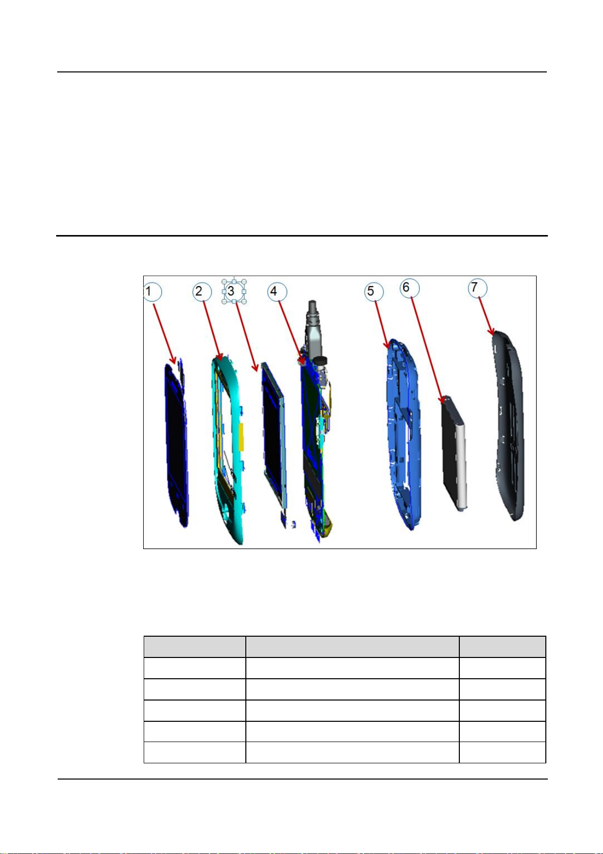
3 Exploded View
No.
Description
Quantity
1
Touch panel (TP)
1
2
Front cover assembly
1
3
LCM
1
4
Printed circuit board assembly (PCBA)
1
5
Rear cover assembly
1
Note: The components listed in the following table are structural parts of the phone, and
cannot be used as reference when requesting spare parts.
Table 3-1 List of components in the exploded view drawing

U8185
Maintenance Manual
3 Exploded View
Issue 1.0 (2012-03-23)
Huawei Proprietary and Confidential
Copyright © Huawei Technologies Co., Ltd.
6
No.
Description
Quantity
6
Battery
1
7
Battery cover
1
U8185
Maintenance Manual
4 Components on the PCBA
Issue 1.0 (2012-03-23)
Huawei Proprietary and Confidential
Copyright © Huawei Technologies Co., Ltd.
7
4 Components on the PCBA
U1204 Accelerometer
chip
Failure of this
component can cause:
Accelerometer failure
J1301 card holder
connector-LCD
Failure of this
component can cause:
No display on the LCD
U3302 RF power
module
Failure of this
component can cause:
Transmit failure
U3202 RF switch
Failure of this
component can cause:
Signal receive or transmit
failure
U3401 RF power
module
Failure of this
component can cause:
Transmit failure-
U3501 RF power
module
Failure of this
component can cause:
Transmit failure
U3304duplexer
Failure of this
component can cause:
No signal; weak signal;
registration failure
U3901 baseband dual
mode RF transception
Failure of this
component can cause:
RF failure
MIC1501 MIC
Failure of this
component can cause:
No sound is picked or
transmitted
U1301 backlight chip
Failure of this
component can cause:
No backlight on the LCD
U8185
Maintenance Manual
4 Components on the PCBA
Issue 1.0 (2012-03-23)
Huawei Proprietary and Confidential
Copyright © Huawei Technologies Co., Ltd.
8
U6000Bluetooth & FM
chip
Failure of this
component can cause:
Bluetooth and FM failure
J901 USB connector
Failure of this
component can cause:
Charging failure; data
communication failure
J1601 TP port
Failure of this
component can cause:
TP does not respond
J902 battery connector
Failure of this
component can cause:
Power-on failure;
charging failure
J1401 SIM/TF card slot
Failure of this
component can cause:
SIM card not identified;
TF card failure
U6100 Wi-Fi chip
Failure of this
component can cause:
Wi-Fi failure
U3101 19.2 MHz clock
Failure of this
component can cause:
No clock; power-on
failure
J1101 headset jack
Failure of this
component can cause:
Headset failure
U601 MCP chip
Failure of this
component can cause:
Power-on failure;
software failure
J1001 camera
connector
Failure of this
component can cause:
Photo or video capture
failure
U6202 RF switch
Failure of this
component can cause:
No Wi-Fi signal
U401 MSM7225A chip
Failure of this
component can cause:
Power-on failure; system
halt; RF failure
U201 PM8029 power
chip
Failure of this
component can cause:
No power output; power-
on failure
BOM
Description
Location
15010251
Schottky diode
D1401, D301, D302
15040311
Transient voltage suppression diode
D1101, D1102, D1103,
D1104, D1501, D1502,
D1503, D1504, D1600,
D1601, D1605, D1606, D901
15020111
Light emitting diode
D1200
19040121
Fuse suite-fast acting fuse
F901
10100150
Terminal dedicated EMI bead
LB1601, LB301, LB302
The following list of components is provided for reference only. This list is subject to change
without notice. The latest component list is available on Huawei's ITEM information system.
If you have any questions, please contact your local technical support.
Table 4-1 Components on the PCBA
U8185
Maintenance Manual
4 Components on the PCBA
Issue 1.0 (2012-03-23)
Huawei Proprietary and Confidential
Copyright © Huawei Technologies Co., Ltd.
9
BOM
Description
Location
10100084
Terminal dedicated EMI bead
LB1102, LB1103, LB1104,
LB1106
22050053
Microphone
MIC1501
15060228
MOSFET-P channel
Q201
15060238
MOSFET-N channel
Q1601
40060329
MCP
U601
38020055
Analog switch-P-channel MOSFET
U1001
38140023
Accelerometer
U1204
39110581
LDO
U1301
12070034
Temperature compensated
oscillator-19.2 MHz
U3101
14240004
RF connector
U3201
47140048
RF switch
U3202
13010186
SAW filter
U3301
47100397
RF power module
U3302
13080065
Duplexer
U3304
47100387
RF power module
U3401
13010189
SAW filter
U3402
13080104
Duplexer
U3404
47100377
RF power module
U3501
13010262
SAW filter
U3702
39200333
Terminal dedicated baseband IC
U3901
13010180
SAW filter
U4102, U4103
47090042
RF low-noise amplifier
U5002
39210040
Bluetooth & FM chip
U6000
39210039
WLAN chip
U6100
47140101
RF switch
U6202
12020125
Crystal resonator
X301
U8185
Maintenance Manual
5 Software Upgrade
Issue 1.0 (2012-03-23)
Huawei Proprietary and Confidential
Copyright © Huawei Technologies Co., Ltd.
10
5.1 Upgrade Preparation
Category
Item
Description
Upgrade
environment
Computer
To copy upgrade software
microSD card
With more than 512 MB free space
Battery
With at least 30% power remaining
Upgrade file
Main upgrade pack
dload/UPDATE.APP
Vendor upgrade pack
vendor_XXX_XXX/UPDATE.APP
Upgrade method
microSD card upgrade
Normal upgrade
Forcible upgrade
5 Software Upgrade
5.2 Upgrade Procedure
1. Format the microSD card.
2. Create a folder named dload in the root directory of the microSD card.
3. Copy the upgrade file to the dload folder.
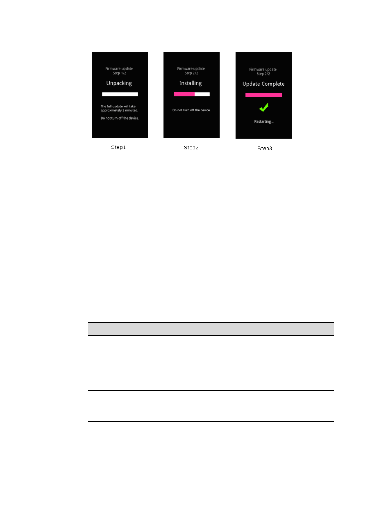
4. Install the microSD card to the phone. Power the phone on, and enter *#*#2846579#*#*
in the idle screen.
5. Select SD card upgrade, and then touch Confirm to start the upgrade.
Before the upgrade, NV items backup is performed (if the phone's NV items has not been
backed up before). Then the phone restarts and the upgrade starts.
The upgrade progress is displayed on the LCD.
U8185
Maintenance Manual
5 Software Upgrade
Issue 1.0 (2012-03-23)
Huawei Proprietary and Confidential
Copyright © Huawei Technologies Co., Ltd.
11
Failure
Solution
The port cannot be found in
USB cable upgrade mode.
Check that there is no other driver conflicting with
the USB driver for the upgrade.
Check that the USB driver has been installed
properly.
Check that the USB cable has been properly
connected.
The phone fails to be upgraded
in USB cable upgrade mode.
Check that the USB cable has been properly
connected.
Perform the upgrade again.
The phone fails to be upgraded
in microSD card upgrade mode.
Check that the upgrade file is correct.
Check that the upgrade method is correct.
Check that the microSD card functions properly.
Perform the upgrade again.
After the upgrade is completed, the phone restarts and the NV items are restored.
6. After the phone is upgraded using the main upgrade pack, upgrade the phone using the
vendor upgrade pack in the same way.
If the phone cannot be properly powered on, use one of the following two methods to forcibly
upgrade the phone:
Install the battery on the phone (if the screen is jittering, remove the battery and wait for
5 seconds before installing the battery again). Press and hold the Volume+ and Volume–
keys, and press the Power key. The phone enters the SD forcible upgrade mode in which
the upgrade process is similar to the normal upgrade.
While the phone has no battery installed, press and hold the Volume+ and Volume– keys,
and connect the charger to the phone. The phone enters the SD forcible upgrade. This
method is recommended. If the forcible upgrade still fails, use another microSD card and
try forcible upgrade again.
5.3 Troubleshooting
U8185
Maintenance Manual
6 Maintenance Tools
Issue 1.0 (2012-03-23)
Huawei Proprietary and Confidential
Copyright © Huawei Technologies Co., Ltd.
12
6 Maintenance Tools
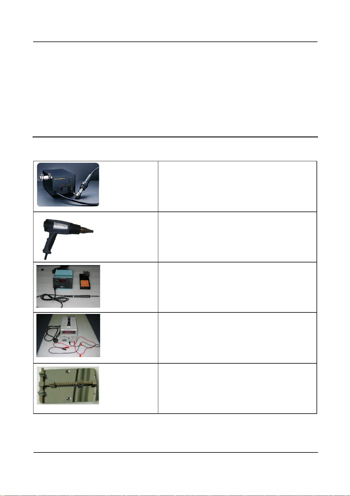
Name: constant-temperature heat gun
Usage: to heat components
Name: constant-temperature heat gun
Usage: to heat components
Name: soldering iron
Usage: to maintain and solder components
Name: DC power supply
Usage: to supply DC current
Name: soldering table
Usage: to secure the PCBA

U8185
Maintenance Manual
6 Maintenance Tools
Issue 1.0 (2012-03-23)
Huawei Proprietary and Confidential
Copyright © Huawei Technologies Co., Ltd.
13
Name: pb-free solder wire
Usage: to solder components
Name: digital multimeter
Usage: to measure during repair
Name: toolkit
Usage: to assemble and disassemble components
Name: electric screwdriver
Usage: to fasten and remove screws
U8185
Maintenance Manual
7 Disassembly Procedure
Issue 1.0 (2012-03-23)
Huawei Proprietary and Confidential
Copyright © Huawei Technologies Co., Ltd.
14
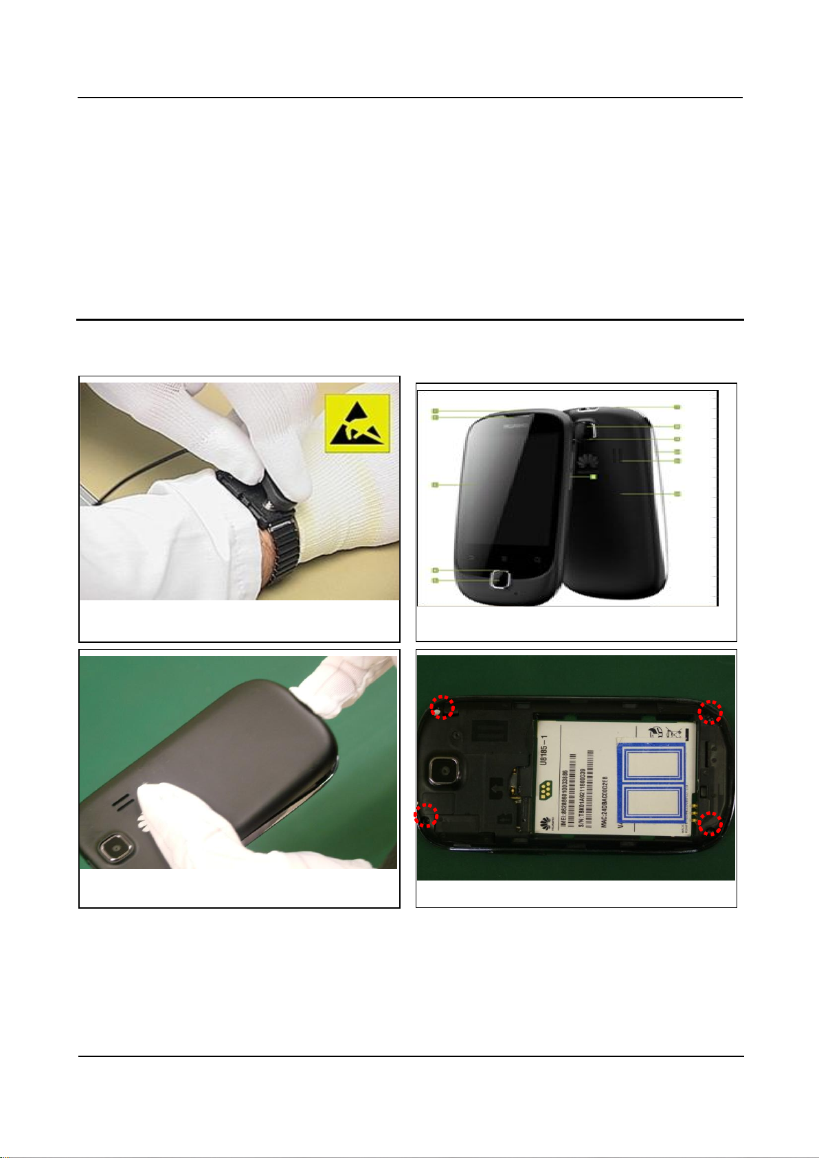
7 Disassembly Procedure
4. Remove the four screws from rear cover.
3. Remove the battery cover.
2. U8185 before disassembly
1. Wear an ESD wrist strap, and ensure that the strap is
grounded properly.
U8185
Maintenance Manual
7 Disassembly Procedure
Issue 1.0 (2012-03-23)
Huawei Proprietary and Confidential
Copyright © Huawei Technologies Co., Ltd.
15
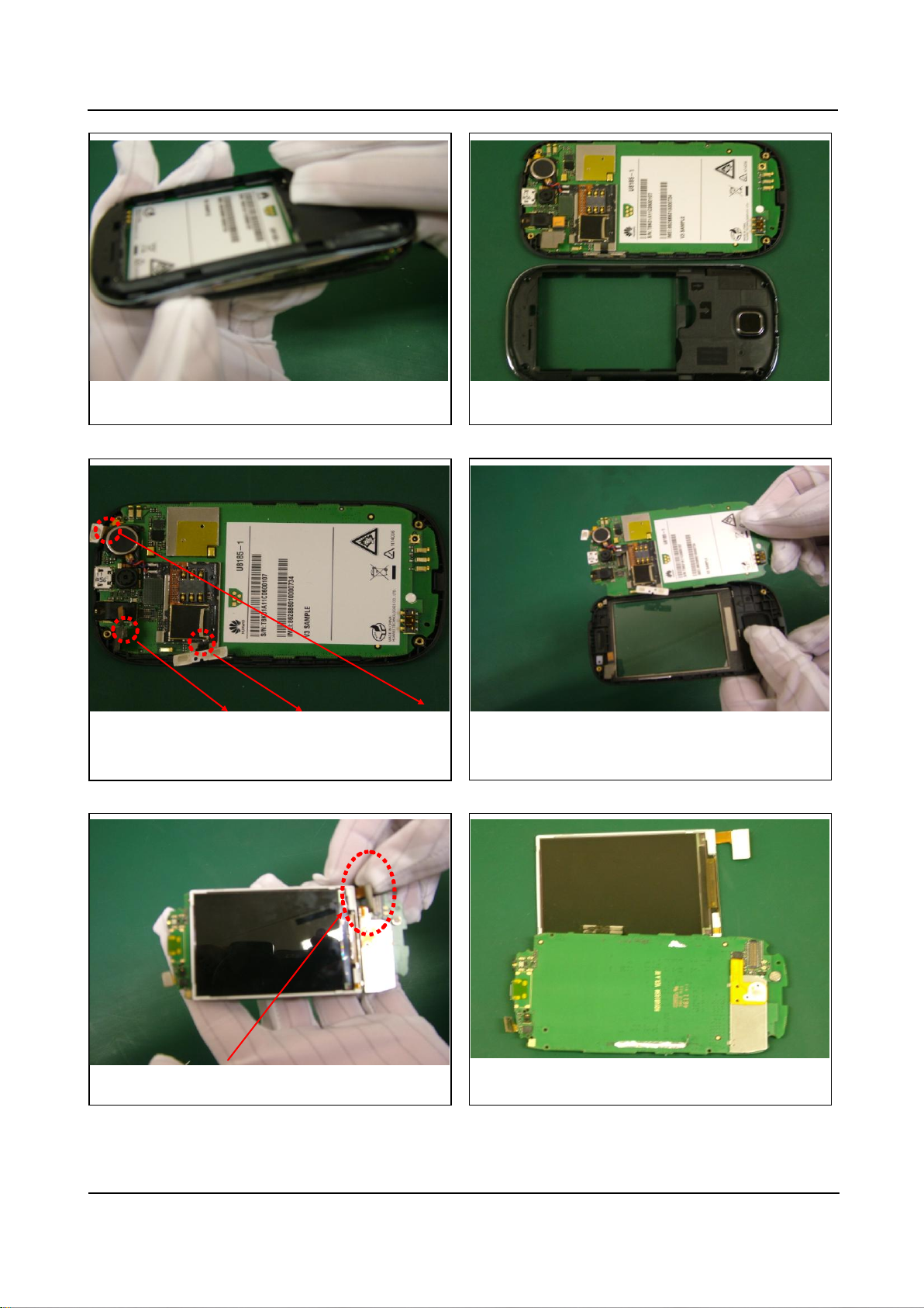
10. Remove the LCD. The phone is then disassembled.
9. Open the LCD connector.
8. Remove the PCBA from the front cover.
7. Use tweezers to release the TP connector, Volume
key dome, and Power key dome.
6. Remove the rear cover.
5. Release the latches between front and rear covers.
U8185
Maintenance Manual
8 Assembly Procedure
Issue 1.0 (2012-03-23)
Huawei Proprietary and Confidential
Copyright © Huawei Technologies Co., Ltd.
16
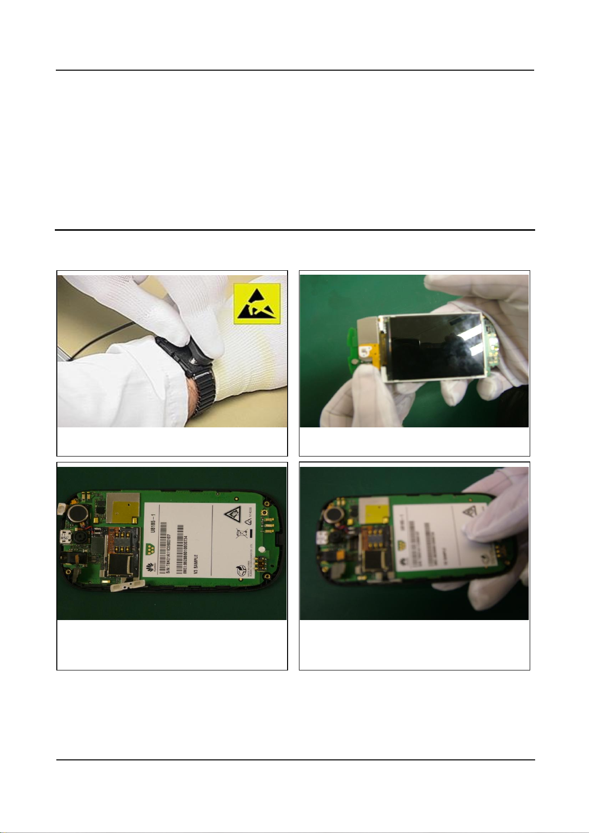
8 Assembly Procedure
4. Install the TP connector, Volume key dome, and
Power key dome, and then snap latch between the
PCBA and front cover in place.
3. Install the PCBA on the front cover. Do not cover
the TP connector FPC under the PCBA.
2. Install the LCD connector.
1. Wear an ESD wrist strap, and ensure that the strap is
grounded properly.
U8185
Maintenance Manual
8 Assembly Procedure
Issue 1.0 (2012-03-23)
Huawei Proprietary and Confidential
Copyright © Huawei Technologies Co., Ltd.
17
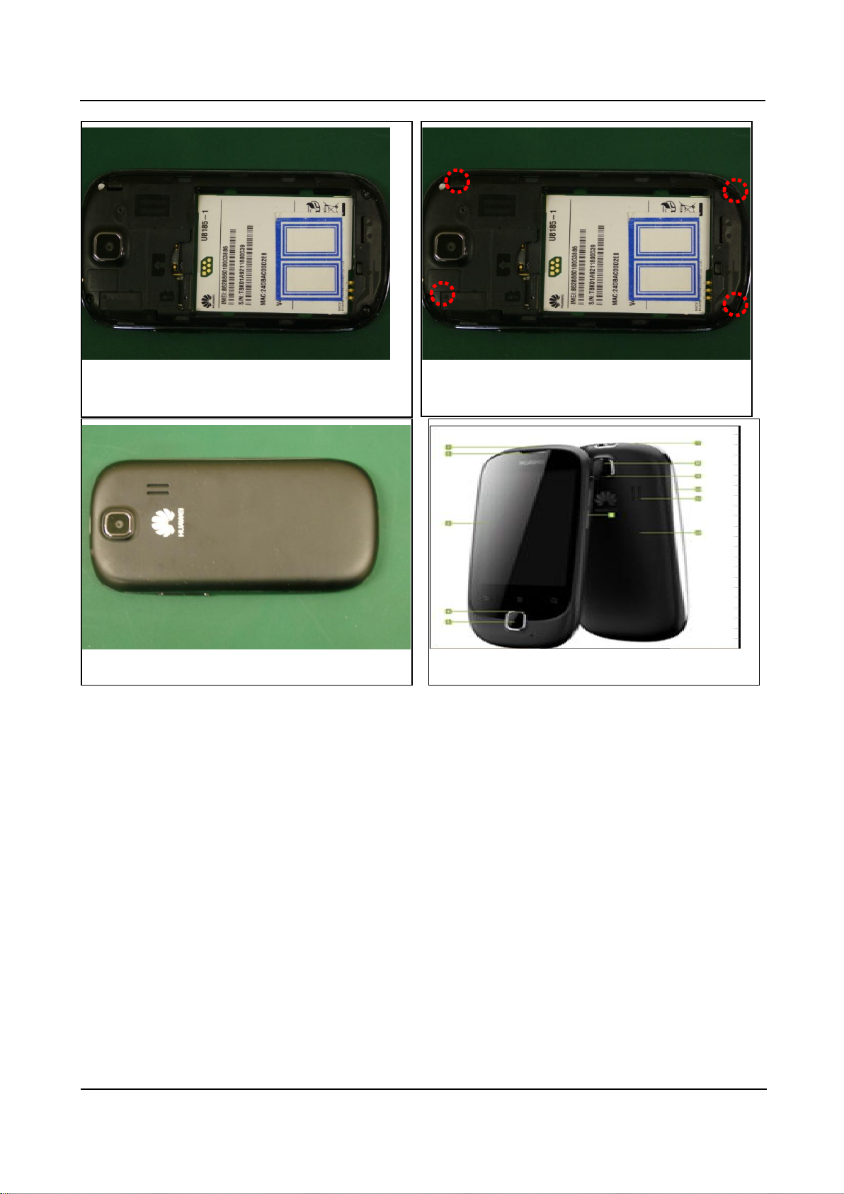
8. The phone is now assembled.
7. Install the battery cover.
6. Install the four screws into the rear cover.
5. Install the Power key and Volume key, and snap the
front and rear covers.

U8185
Maintenance Manual
9 Principles and Failure Analysis
Issue 1.0 (2012-03-23)
Huawei Proprietary and Confidential
Copyright © Huawei Technologies Co., Ltd.
18
9 Principles and Failure Analysis
HD1U8185M.pdf
Before repairing a phone, ensure that the failure of the phone is not caused by environmental
factors or incorrect functional settings. It is recommended that you restore the phone to its
factory settings.
9.1 Block Diagram
Figure 9-1 U8185 block diagram
U8185
Maintenance Manual
9 Principles and Failure Analysis
Issue 1.0 (2012-03-23)
Huawei Proprietary and Confidential
Copyright © Huawei Technologies Co., Ltd.
19
The MSM7X2XA (the U8185 uses the MSM7225A) is the baseband signal processing chip,
mainly responsible for processing the input and output of IMAGE, VIDEO, AUDIO, RF
INTERFACES, and CONECTIVITY signals. The baseband chip provides keypad, LCD,
microSD card, Wi-Fi, camera, and microphone interfaces.
The PM8029 provides analog multi-channel switch, real-time clock circuit, TCXO clock
circuit, motor driver circuit, and programmable current source.
The RTR6285A is the RF signal processing chip, responsible for converting uplink/downlink
RF signals.
The PCBA can be divided into four sub-systems: baseband, RF, power supply, and user
interfaces.
9.2 Baseband Unit
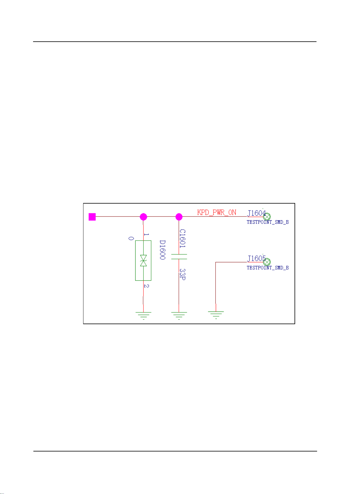
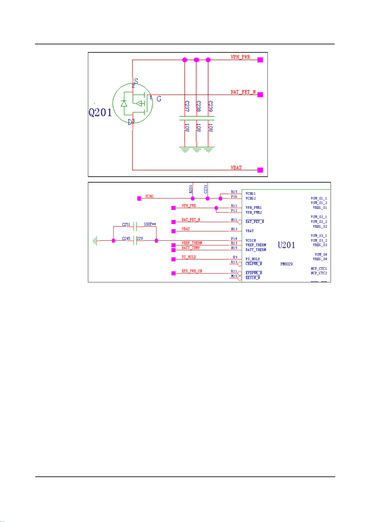
9.2.1 Power-on Management Circuits
Figure 9-2 Circuit schematic diagram
U8185
Maintenance Manual
9 Principles and Failure Analysis
Issue 1.0 (2012-03-23)
Huawei Proprietary and Confidential
Copyright © Huawei Technologies Co., Ltd.
20
Analysis
After the Power key is pressed, the phone powers on. VHP_PWR (main power voltage)
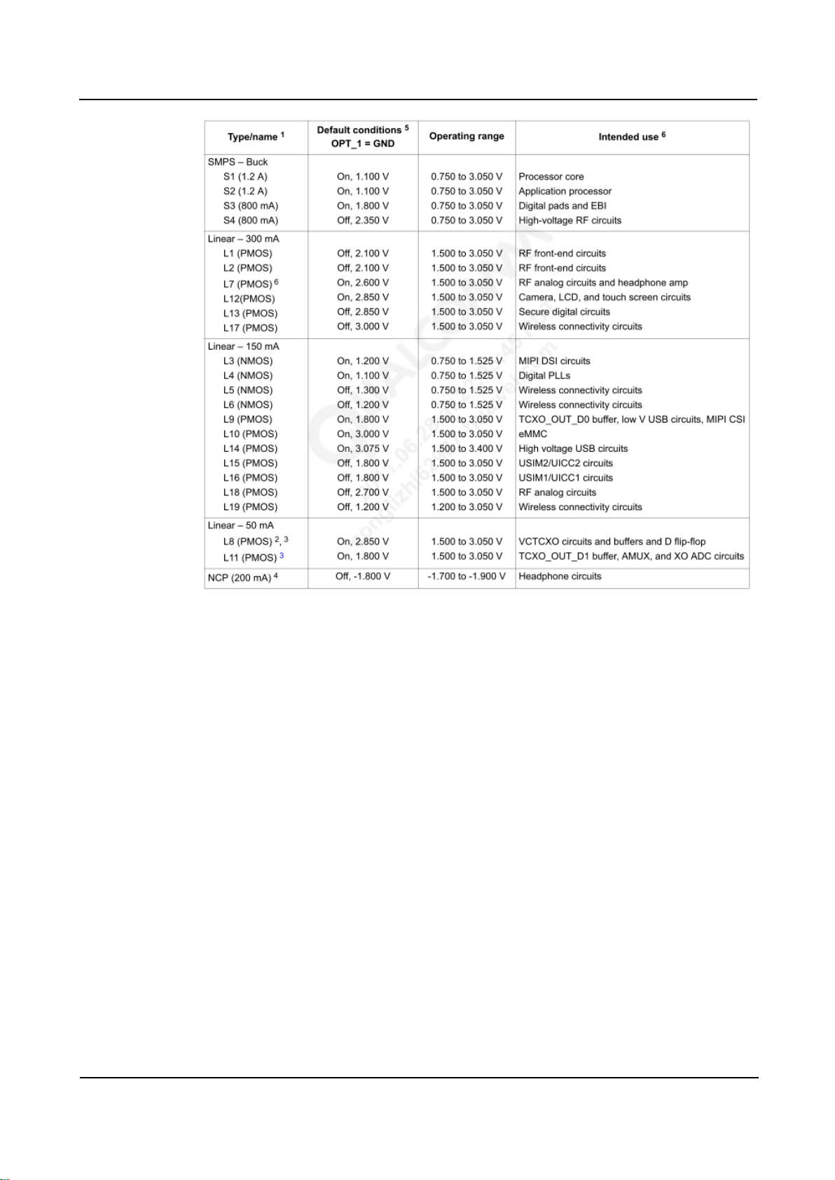
powers the PM8029. The power management chip then provides the voltages listed in the
following table.
U8185
Maintenance Manual
9 Principles and Failure Analysis
Issue 1.0 (2012-03-23)
Huawei Proprietary and Confidential
Copyright © Huawei Technologies Co., Ltd.
21
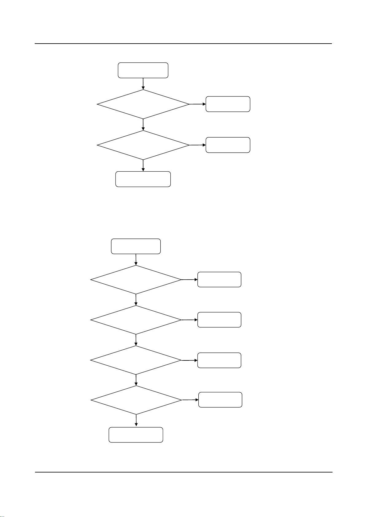
Troubleshooting Process
Fault symptom: power-on failure
To troubleshoot the power-on failure, firstly check whether the I/O connector (battery
connector) is damaged. If the I/O connector (battery connector) is not damaged, use a DC
regulated power supply to supply power to the phone, and test the phone's current.
The power-on failure may be caused by any of the following conditions:
No current
U8185
Maintenance Manual
9 Principles and Failure Analysis
Issue 1.0 (2012-03-23)
Huawei Proprietary and Confidential
Copyright © Huawei Technologies Co., Ltd.
22
Replace J902
N
Power-on failure:
no current
Is the battery
connector J902
normal?
Replace Q201
N
Is Q201 normal?
Y
Re-solder or replace
U201
Y
End
Y
Power-on failure:
weak current
Re-install the phone's
software. Is the problem
solved?
Is U201's output
voltage normal?
Replace U201
N
N
Replace U401
N
Does X301 have
32.768 kHz output?
Replace U601 and re-install
the phone's software. Is the
problem solved?
Y
Replace X301
N
End
Y
Y
Weak current
 Loading...