

Huawei MediaPad 10 FHD Maintenance Manual V1.0
MediaPad10 FHD Maintenance Manual INTERNAL
MediaPad 10 FHD Maintenance Manual
V1.0
For internal use only
Prepared by
Reviewed by
Approved by
Yang Yongxiang
Zhang Dewen
Zhen Haitao
Date
Date
Date
2012-7-14
Huawei Technologies Co., Ltd.
All right reserved
2012-10-09 Huawei Confidential Page 1 of 78

MediaPad10 FHD Maintenance Manual INTERNAL
Change History
Date Revision Version Change Reason Changed Chapter Change Description Author
2012-7-14 V1.0
2012-10-09 Huawei Confidential Page 2 of 78

MediaPad10 FHD Maintenance Manual INTERNAL
Contents
1 Product Overview .................................................................................................................... 8
1.1 Brief Introduction ....................................................................................................................................... 8
1.2 Hardware Specifications ........................................................................................................................... 11
1.3 Software Specifications ............................................................................................................................ 12
1.4 Exploded View of the Host ....................................................................................................................... 12
2 Functional Chips .................................................................................................................... 14
2.1 Hi3620 ..................................................................................................................................................... 14
2.1.1 Chip Specifications .......................................................................................................................... 14
2.1.2 Pin Assignment ................................................................................................................................ 15
2.1.3 Working Principles and Functions of the Hi3620 .............................................................................. 15
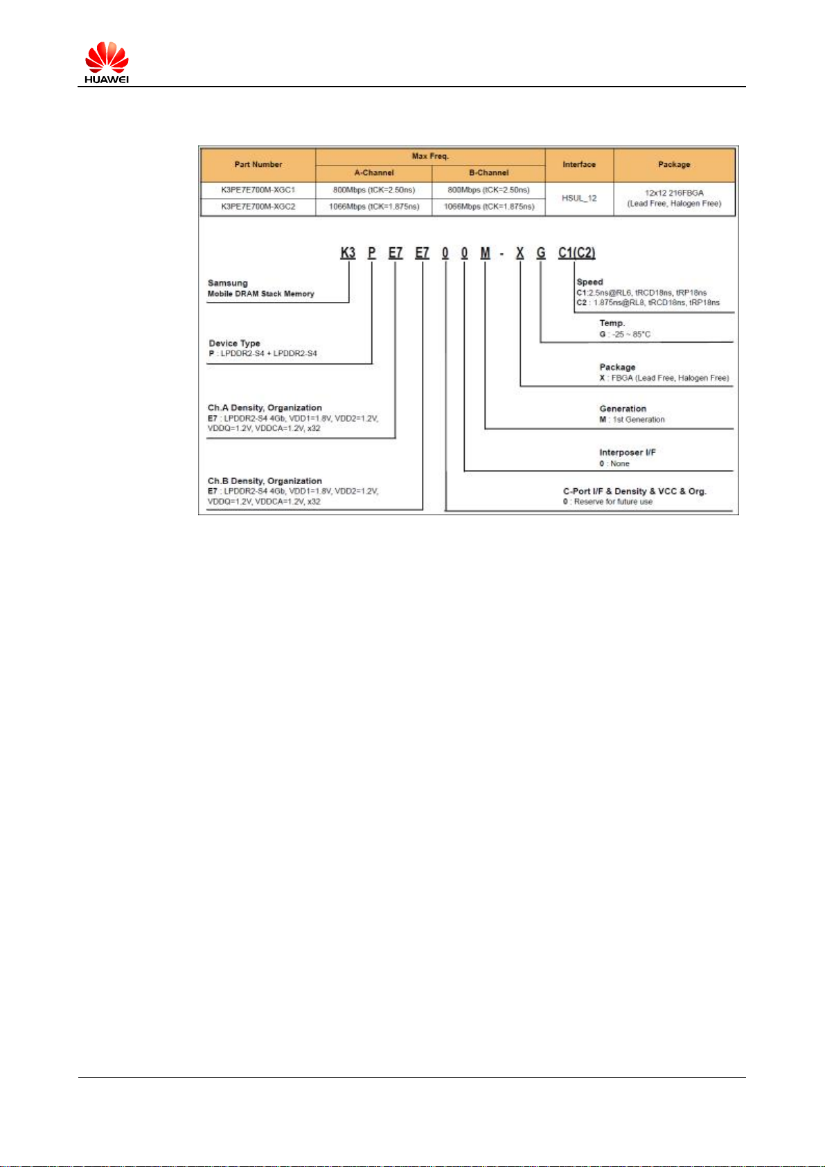
2.2 POP LPDDR2 .......................................................................................................................................... 17
2.3 PMU Hi6421 ............................................................................................................................................ 20
2.4 Wi-Fi and Bluetooth Modules ................................................................................................................... 25
2.5 GPS BCM47511 ....................................................................................................................................... 28
3 Layout of Major Components .............................................................................................. 32
3.1 Layout of Components on the S10 PCBA ................................................................................................. 32
3.2 Components on the S10 PCBA ................................................................................................................. 32
4 Principles and Failure Analysis ........................................................................................... 37
4.1 Working Principles of the MediaPad 10 FHD ............................................................................................ 37
4.2 Power-On and Power Tree ........................................................................................................................ 39
4.2.1 Hardware Startup Process ................................................................................................................ 39
4.2.2 Power Tree ...................................................................................................................................... 41
4.3 Circuit Analysis and Troubleshooting for Functional Units ........................................................................ 42
4.3.1 Working Principles of the AP Subsystem .......................................................................................... 42
4.3.2 Detailed Analysis of Working Principles of the AP Subsystem .......................................................... 45
4.4 Circuit Analysis and Troubleshooting for the Modem Unit ........................................................................ 65
5 Software Upgrade .................................................................................................................. 73
5.1 Upgrade Preparation ................................................................................................................................. 73
5.2 Upgrading the Software by Using a USB Peripheral .................................................................................. 73
5.2.1 Upgrading the Software by Using a microSD Card ........................................................................... 73
6 Disassembly Procedure ......................................................................................................... 75
2012-10-09 Huawei Confidential Page 3 of 78

MediaPad10 FHD Maintenance Manual INTERNAL
6.1 Tools ........................................................................................................................................................ 75
6.2 Disassembly Preparation........................................................................................................................... 75
6.3 Disassembly Procedure ............................................................................................................................. 75
6.4 Other Precautions ..................................................................................................................................... 75
7 Appendix ................................................................................................................................. 77
7.1 PCBA Layout ........................................................................................................................................... 77
7.2 Test Spot List ........................................................................................................................................... 78
7.3 Acronyms and Abbreviations .................................................................................................................... 78
2012-10-09 Huawei Confidential Page 4 of 78

MediaPad10 FHD Maintenance Manual INTERNAL
Figures
Figure 1-1 Appearance of the MediaPad 10 FHD ............................................................................................. 9
Figure 1-2 Hardware principles of the MediaPad 10 FHD .............................................................................. 10
Figure 1-3 Exploded view of the host ............................................................................................................. 13
Figure 2-1 Functional blocks of the Hi3620 ................................................................................................... 14
Figure 2-2 Functional blocks of the POP LPDDR2 chip ................................................................................. 18
Figure 2-3 Model of the POP LPDDR2 chip provided by ELPIDA ................................................................. 18
Figure 2-4 Model of the POP LPDDR2 chip provided by Samsung ................................................................ 19
Figure 2-5 Pinouts of the POP LPDDR2 chip ................................................................................................. 20
Figure 2-6 Functional blocks of the power supply .......................................................................................... 23
Figure 2-7 RF solution for the Wi-Fi and Bluetooth modules of the S10 ......................................................... 26
Figure 2-8 Components encapsulated in the WI-FI or Bluetooth module ......................................................... 28
Figure 2-9 RF solution for the GPS module of the S10 ................................................................................... 29
Figure 2-10 Functional blocks of the BCM47511 chip .................................................................................... 30
Figure 2-11 Models of the BCM47511 ........................................................................................................... 30
Figure 2-12 Components encapsulated in the BCM47511 chip ....................................................................... 31
Figure 3-1 Layout of components on the S10 PCBA ...................................................................................... 32
Figure 4-1 Functional blocks of the PCBA ..................................................................................................... 38
Figure 4-2 Layout of components on the PCBA ............................................................................................. 38
Figure 4-3 Physical architecture of the PCBA ................................................................................................ 39
Figure 4-4 Power-on and power-off sequencing ............................................................................................. 40
Figure 4-5 Power-on procedure ...................................................................................................................... 41
Figure 4-6 AP framework .............................................................................................................................. 42
Figure 4-7 Working principles of the PMU ..................................................................................................... 45
Figure 4-8 Possible faults of the AP power circuit .......................................................................................... 47
Figure 4-9 Working principles of the AP charging circuit................................................................................ 49
Figure 4-10 Working principles of the coulometer circuit ............................................................................... 50
2012-10-09 Huawei Confidential Page 5 of 78

MediaPad10 FHD Maintenance Manual INTERNAL
Figure 4-11 Working principles of the eMMC circuit...................................................................................... 52
Figure 4-12 Working principles of the MIC circuit ......................................................................................... 53
Figure 4-13 Working principles of the headset circuit ..................................................................................... 54
Figure 4-14 Working principles of the LCD circuit ......................................................................................... 55
Figure 4-15 Working principles of the TP circuit ............................................................................................ 57
Figure 4-16 Working principles of the rear camera ......................................................................................... 59
Figure 4-17 Working principles of the front camera ........................................................................................ 59
Figure 4-18 Working principles of the BC1.1 circuit....................................................................................... 60
Figure 4-19 Working principles of the charging circuit ................................................................................... 62
Figure 4-20 Working principles of the MAX8903A ........................................................................................ 62
Figure 4-21 Working principles of the sensor circuits ..................................................................................... 64
Figure 4-22 Circuits of the modem unit .......................................................................................................... 66
Figure 7-1 PCBA layout at the top layer ......................................................................................................... 77
Figure 7-2 PCBA layout at the bottom layer ................................................................................................... 77
2012-10-09 Huawei Confidential Page 6 of 78

MediaPad10 FHD Maintenance Manual INTERNAL
Tables
Table 1-1 External hardware interfaces ........................................................................................................... 11
Table 1-2 Hardware specifications of the MediaPad 10 FHD .......................................................................... 11
Table 3-1 Description of components on the S10 PCBA ................................................................................. 32
Table 4-1 Voltage signals of the AP power circuit ........................................................................................... 45
Table 4-2 Possible faults of the AP power circuit ............................................................................................ 47
Table 4-3 Definitions of signals of the AP charging circuit .............................................................................. 50
Table 4-4 Definitions of signals of the coulometer circuit ............................................................................... 51
Table 4-5 Definitions of signals of the eMMC circuit ..................................................................................... 52
Table 4-6 Definitions of signals of the MIC circuit ......................................................................................... 53
Table 4-7 Definitions of signals of the headset circuit ..................................................................................... 55
Table 4-8 Definitions of signals of the LCD circuit ......................................................................................... 57
Table 4-9 Definitions of signals of the TP circuit ............................................................................................ 58
Table 4-10 Definitions of signals of the camera circuit ................................................................................... 60
Table 4-11 Definitions of signals of the BC1.1 circuit ..................................................................................... 61
Table 4-12 Definitions of signals of the charging circuit ................................................................................. 63
Table 4-13 Definitions of signals of the sensor circuit ..................................................................................... 65
Table 5-1 Upgrade preparation ....................................................................................................................... 73
Table 7-1 Test spot list ................................................................................................................................... 78
2012-10-09 Huawei Confidential Page 7 of 78

MediaPad10 FHD Maintenance Manual INTERNAL
1.1 Brief Introduction
Background
10-inch tablets take a share of more than 70% of the tablet market. As a mainstream model of
tablets, they provide Internet surfing, pleasant visual experience, and portable use. 10-inch
tablets have found their way in a variety of application fields, such as retailing, operators'
mobile broadband product reselling, operators' promotion of new home products, enterprise
office administration, and financial insurance.
1 Product Overview
MediaPad 10 FHD is a 10-inch tablet of Huawei MediaPad series based on the Android 4.0
(Ice Cream Sandwich) operating system. Its hardware integrates an access point (AP) and a
modem (K3+BalongV7). Equipped with a 10.1-inch in-plane switching (IPS) thin-film
transistor (TFT) LCD, the MediaPad 10 FHD features high resolution (1920 x 1200 pixels)
and provides complete touchscreen operations. It supports multiple audio and video formats,
such as MP3, MP4, AVI, ASF, and WAV.
The MediaPad 10 FHD also provides the following auxiliary functions:
l
8.0 megapixel (MP) camera
l
microSD card
l
Global positioning system (GPS)
l
Wireless Fidelity (Wi-Fi)
l
Bluetooth 4.0
l
Frequency modulation (FM)
l
Acceleration sensor
l
Proximity sensor
l
Light sensor
l
Gyroscope sensor
l
Compass
l
Electromagnetic sensor
In terms of wireless communication, the MediaPad 10 FHD supports the following features:
l
GSM mode: GPRS and EDGE
l
WCDMA mode: UMTS, HSDPA, and HSPA+
l
WCDMA frequency bands: bands 1, 2, 5, 8, 9, and 11
l
GSM frequency bands: 850 MHz, 900 MHz, 1800 MHz, and 1900 MHz.
2012-10-09 Huawei Confidential Page 8 of 78
MediaPad10 FHD Maintenance Manual INTERNAL
The entire device has five antennas: one host antenna, one diversity antenna, one GPS antenna,
one antenna for the Bluetooth and Wi-Fi modules, and one independent antenna for the
synthetic aperture radar (SAR) sensor.
The smart chip MAX8903 is used for charging management, the Broadcom BCM4330 chip is
used for the Wi-Fi and Bluetooth modules, and the BCM47511 chip is used for the GPS
module.
The MediaPad 10 FHD has the following memory features:
l
AP RAM: LP DDR2, standard 1 GB 533 Hz (compatible with 2 GB)
l
AP ROM: eMMC, standard 8 GB (compatible with 16 GB and 32 GB)
l
Modem: Hi6920+Hi6451+Hi6360, MCP (NAND+DDR), standard 2 Gbit + 1 Gbit
(compatible with 1 Gbit + 512 Mbit)
The MediaPad 10 FHD supports the 3.5 mm headset jack and 30-pin dock interface. The dock
interface supports multiple functions, such as charging, power supply, USB host or device
installation, and the display port.
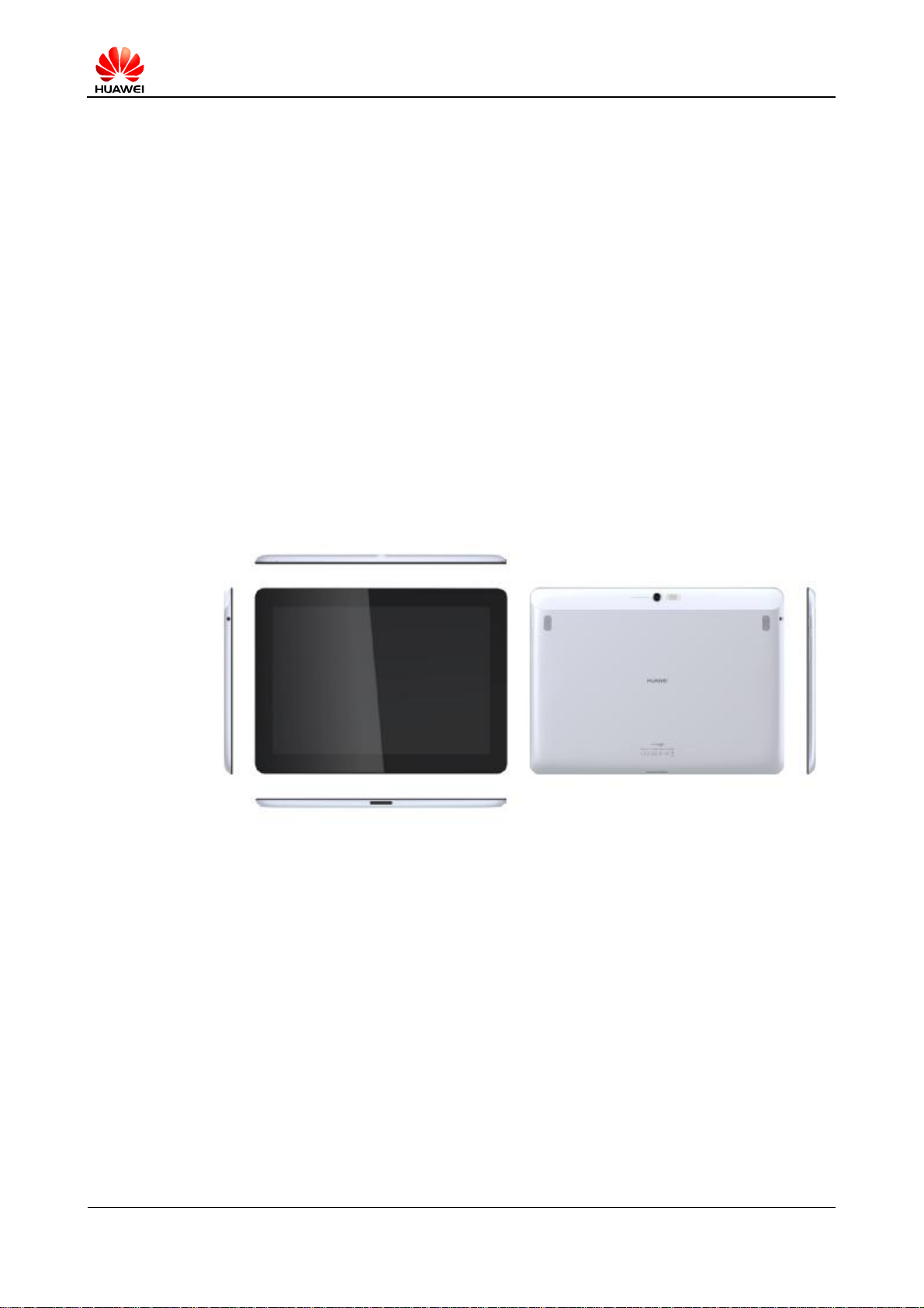
Figure 1-1 shows the appearance of the MediaPad 10 FHD.
Figure 1-1 Appearance of the MediaPad 10 FHD
Figure 1-2 shows the hardware principles of the MediaPad 10 FHD (Hi3620+Hi6920).
2012-10-09 Huawei Confidential Page 9 of 78
MediaPad10 FHD Maintenance Manual INTERNAL
Figure 1-2 Hardware principles of the MediaPad 10 FHD
Board Functions
The main control board provides the following functions:
l
Provides the host CPU and processes image signals.
l
Manages host power supply.
l
Supports UMTS (WCDMA), HSPA, GSM, GPRS, and EDGE.
l
Supports GPS.
l
Provides LCD and camera interfaces.
l
Provides audio interfaces.
l
Provides a WLAN or Bluetooth module.
The interface board provides the following functions:
l
Provides dock interfaces.
l
Provides USB and charging interfaces.
Table 1-1 lists the hardware interfaces provided by the MediaPad 10 FHD.
2012-10-09 Huawei Confidential Page 10 of 78
MediaPad10 FHD Maintenance Manual INTERNAL
Table 1-1 External hardware interfaces
No. Interface
Type
1 USB OTG 1 This interface is used to connect to a PC or other
2 3G Main antenna and
3 WLAN Built-in antenna 1 This interface is used to connect to a local
4 Dock
interface
5 Power switch Tact switch 1 Power switch
6 Key Sound volume
7 Touchscreen Capacitor screen,
8 LCD MIPI 1 1920 x 1080 pixels
Physical
Interface Mode
diversity antenna
Dock jack 1 This interface provides numerous
adjustment key
I2C interface
Number of
Interfaces
2 This interface is an uplink data interface for
2 VOL+, VOL-
1 Compatible with the resistor-capacitor
Remarks
devices. It complies with the USB 2.0
specification.
voice services (WCDMA).
WLAN device.
communication signals, such as power input,
MHL, and USB signals.
9 JTAG
interface
10
11
12
13
Normalized 9-pin
encapsulation
1 This JTAG interface is used for program
1.2 Hardware Specifications
Table 1-2 lists the hardware specifications of the MediaPad 10 FHD.
Table 1-2 Hardware specifications of the MediaPad 10 FHD
Technical Parameter Specification
Dimensions (H x W x D) 8.9 mm x 267.2 mm x 169.8 mm
Weight About 630 g (TBD)
loading.
2012-10-09 Huawei Confidential Page 11 of 78
MediaPad10 FHD Maintenance Manual INTERNAL
Technical Parameter Specification
Shape
Battery 6300 mA
Display 10.1-inch WXGA (1920 x 1200 pixels), TFT, touchscreen
Touch panel Capacitive, Multi-touch (10 points)
Interface 30-pin dock connector
3.5 mm headset jack
Band S10-101u: UMTS 2100/900, EDGE/GPRS/GSM (850/900/1800/1900)
S10-102u: UMTS 2100/1900/850, EDGE/GPRS/GSM (850/900/1800/1900)
HSPA+: 42 Mbit/s
Chipset Hi3620T (K3 V2) + Hi6920 (Balong V7)
OS Android 4.0 (Ice Cream Sandwich)
Memory RAM: 2 GB
ROM: 16 GB
Maximum 32 GB microSD card
Multimedia Rear camera: 8.0 MP HD AF, dual LED flash
Front camera: 1.3 MP HD
H.263, MPEG4, H.264 (decode)
MP3, AAC, AAC+
Network service 3G
Others Wi-Fi b/g/n, Bluetooth v3.0 +HS, DLNA, 30-pin dock connector, 1080p video
1.3 Software Specifications
1.4 Exploded View of the Host
Figure 1-3 shows the exploded view of the host.
2012-10-09 Huawei Confidential Page 12 of 78
MediaPad10 FHD Maintenance Manual INTERNAL
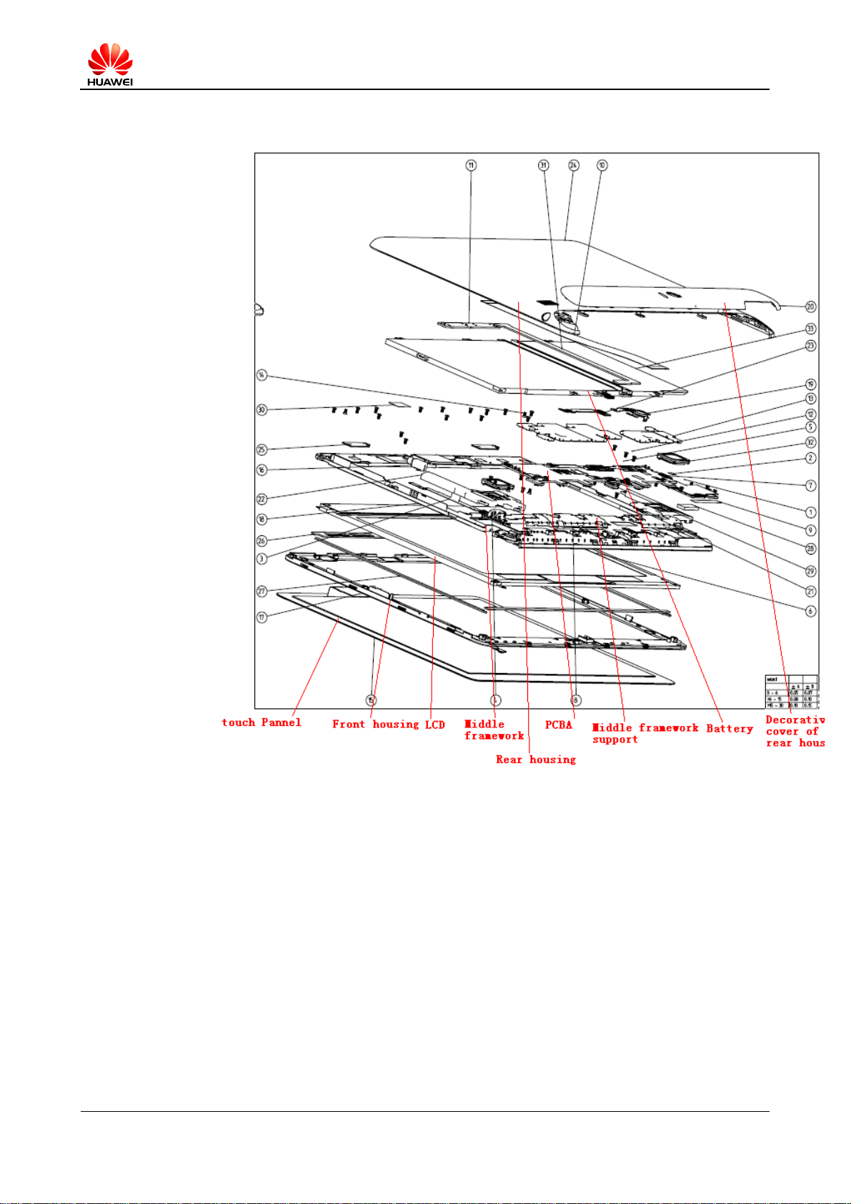
Figure 1-3 Exploded view of the host
2012-10-09 Huawei Confidential Page 13 of 78
MediaPad10 FHD Maintenance Manual INTERNAL
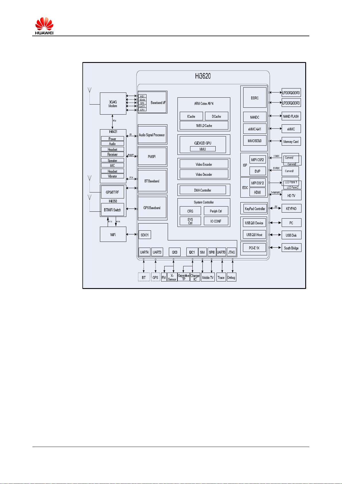
2.1 Hi3620
2 Functional Chips
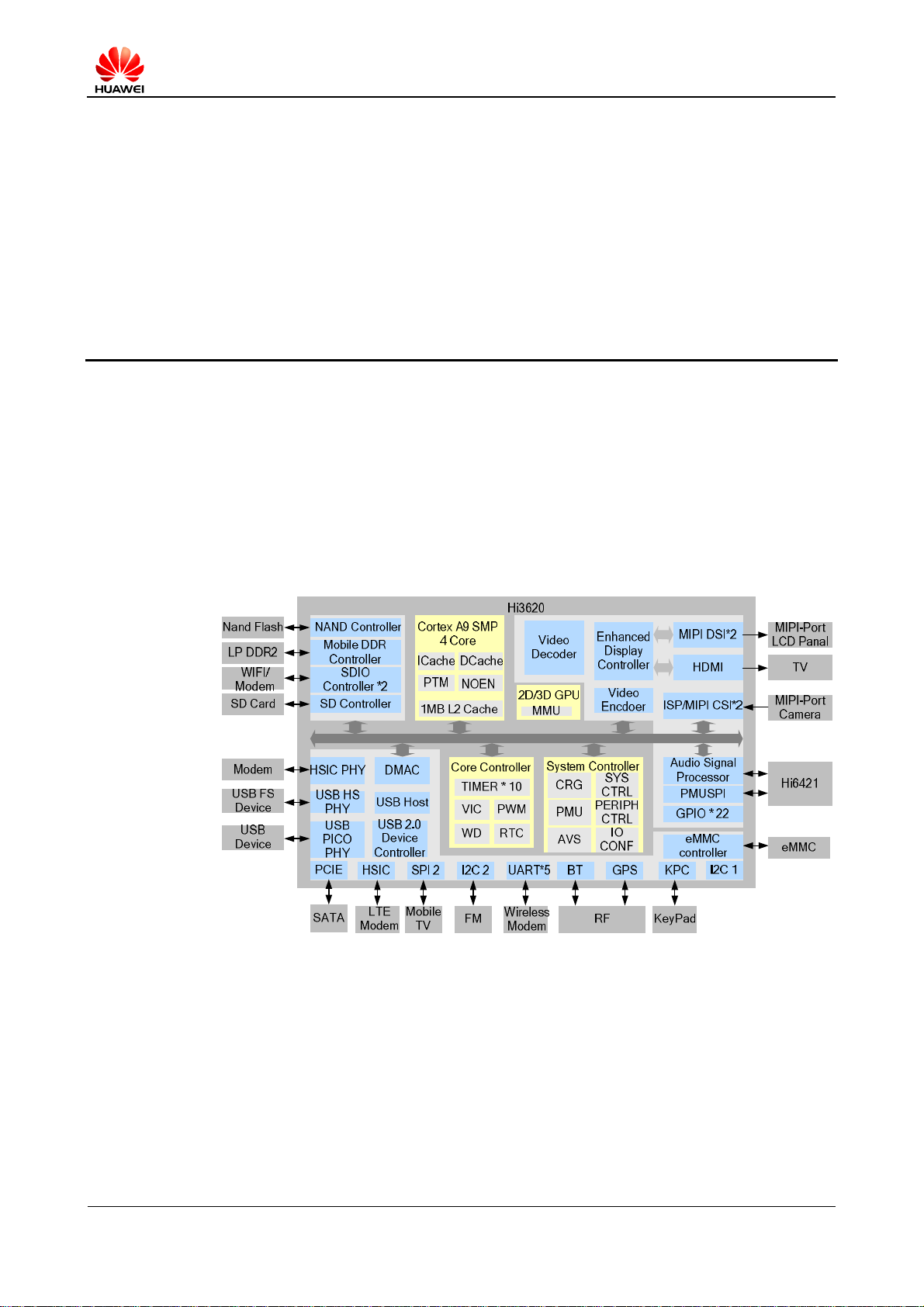
The Hi3620 is a new-generation quad core ARM cortex-A9 processor launched by Hisilicon.
The processor supports 1.2 GHz processing.
Figure 2-1 shows the functional blocks of the Hi3620.
Figure 2-1 Functional blocks of the Hi3620
2.1.1 Chip Specifications
Encapsulation: 11.90 mm x 11.90 mm, 576-pin BGA/CSP encapsulation, Hi3620 (IC).
2012-10-09 Huawei Confidential Page 14 of 78

MediaPad10 FHD Maintenance Manual INTERNAL
2.1.2 Pin Assignment
2.1.3 Working Principles and Functions of the Hi3620
The K3V200 system uses the Hi3620 chip as its core to provide the following logical
interfaces:
NAND/eMMC Interface
The Hi3620 provides 16-bit NAND interfaces. The high 8-bits are multiplexed with the
eMMC interface. Therefore, it is recommended that the eight high-order bits be connected to
the eMMC component and the eight low-order bits be connected to a component such as the
MLC NAND or Clear NAND.
Camera Interface and LCD Interface
The Hi3620 provides three MIPI interfaces: CSI0, DSI0, and CSI_DSI1. Each interface can
contain four data lanes. The Hi3620 also provides one parallel camera interface which is
known as the DVP interface.
l
CSI0: This interface is used for camera image capturing.
l
DSI0: This interface is used for LCD display.
l
CSI1_DSI1: This interface can be statically multiplexed as an LCD display interface (in
the two-screen application scenario) or as an interface for camera image capturing (in 3D
image pickup and master/master camera application scenarios).
l
DVP: This interface is used to connect to a camera through a parallel bus. It is reserved
for the front camera.
microSD Card Interface
The Hi3620 provides a dedicated microSD card slot, which complies with the SD3.0
specification and supports the SDR50 or DDR50.
The bus clock frequency of the SDR50 is 100 MHz, and that of the DDR50 is 50 MHz.
SDIO Interface
The Hi3620 provides two SDIO buses, which comply with the SD2.0 specification and
support at most the SDR25. The two buses are used to connect peripherals.
l
SDIO0: This interface is the data and control interface of the AP or modem. Its signal
level is 1.8 V or 2.5 V.
l
SDIO1: This interface is the data and control interface of Wi-Fi. Its signal level is 1.8 V.
The bus clock frequency of the SDR25 is 50 MHz.
UART Interface
The Hi3620 provides five UART interfaces, all of which support four-wire hardware flow
control and provide the maximum baud rate of 3.25 Mbit/s. These interfaces are used to
connect to peripherals.
2012-10-09 Huawei Confidential Page 15 of 78

MediaPad10 FHD Maintenance Manual INTERNAL
SPI Interface
l
UART0: This UART interface is specially used for system commissioning or loading. Its
signal level is 2.5 V.
l
UART1: This interface is used as the data and control interface of the AP or modem. It
can also be multiplexed as a GPIO interface. Its signal level is 1.8 V or 2.5 V.
l
UART2: This interface is statically multiplexed with USIM and onewire signals and
reserved for peripherals. Its signal level is 1.8 V.
l
UART3: This interface is multiplexed with the GPS baseband bus GPS_SPI that is
integrated in the Hi3620. It provides a data and control channel for external third-party
GPS devices. Its signal level is 1.8 V.
l
UART4: This interface is multiplexed with the Bluetooth baseband interface BT_IF that
is integrated in the Hi3620. It provides a data and control channel for external third-party
Bluetooth devices. Its signal level is 1.8 V.
The Hi3620 supports five groups of SPI bus interfaces, all of which work in master mode.
l
SPI0: This SPI interface supports a maximum of four chip selection signals. It is
reserved for peripherals, such as the CMMB. Its signal level is 1.8 V.
l
SPI1: This interface is the communication and control interface of the modem. Its signal
level is 1.8 V or 2.5 V.
l
PMU_SPI: This SPI interface is dedicated for the PMU (Hi6421) and works in
three-wire mode (the input end and the output end share the same data signal). Its signal
level is 1.8 V.
l
BT_SPI: This interface is a dedicated SPI interface between a Bluetooth baseband unit
integrated in the Hi3620 and the RF IC (Hi6350). Its signal level is 1.8 V.
l
GPS_SPI: This interface is a dedicated SPI interface between a GPS baseband unit
integrated in the Hi3620 and the RF IC (Hi6350). Its signal level is 1.8 V.
I2C Bus
The Hi3620 provides four groups of I2C buses. Two groups are dedicated for camera
interfaces, and the other two groups are used for peripherals.
l
ISP_I2C0/1: used for camera I2C interfaces.
l
I2C0: used for the xSenor, capacitive touchscreen, and independent FM communication
and data interfaces.
l
I2C1: used for the charging IC.
The xSensor and capacitive touchscreen are components that may be frequently accessed. Therefore, the
preceding I2C bus allocation mode is applied by default but a jumper is reserved during design to
connect the capacitive touchscreen to I2C1.
Digital Audio Interface PCM/I2S
The K3V200 system provides three groups of digital audio interfaces to connect to a codec
inside the Hi6421.
l
I2S interface: This interface is a stereo audio interface between the Hi3620 and the codec
inside the Hi6421.
l
M_PCM interface: This interface provides a voice channel between the modem and the
codec inside the Hi6421.
2012-10-09 Huawei Confidential Page 16 of 78

MediaPad10 FHD Maintenance Manual INTERNAL
l
HDMI Interface
The Hi3620 complies with the HDMI1.3a protocol specification. It supports high-definition
playing (up to 1080p) and provides HDMI interfaces to connect to external display devices.
HSIC Interface
The Hi3620 provides the HSIC interface as the active high-rate communication and control
interface between the AP and the modem.
USB Interface
The Hi3620 provides two USB2.0 interfaces, both of which support the highest speed 480
Mbit/s.
l
l
BT_PCM interface: This interface provides a voice channel between external third-party
Bluetooth devices and the codec inside the Hi6421.
USB_NANO interface: This interface statically supports USB 2.0 hosts and devices.
USB_PICO interface: This interface supports USB2.0 devices and BC1.1 (in compliance
with a charging specification supplementary to the USB2.0 specification).
PCIe Interface
The Hi3620 supports one PCIe 1.0 interface, which is reserved for external devices, such as a
South Bridge or SATA disk.
2.2 POP LPDDR2
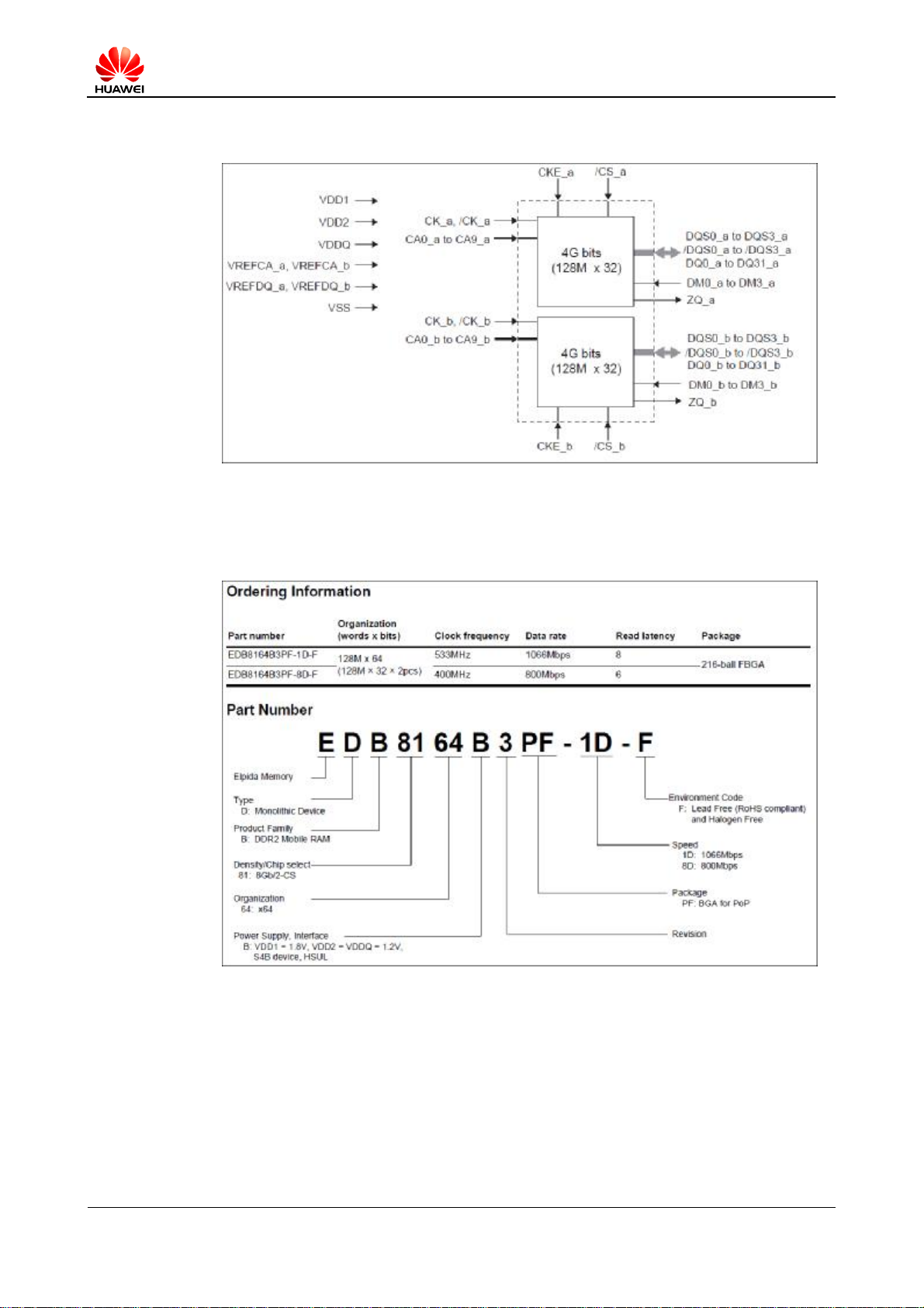
The DDR2 chip uses the POP encapsulation technology. Currently, two vendors ELPIDA and
Samsung supply this chip to Huawei.
Figure 2-2 shows the functional blocks of the POP LPDDR2 chip.
2012-10-09 Huawei Confidential Page 17 of 78
MediaPad10 FHD Maintenance Manual INTERNAL
Figure 2-2 Functional blocks of the POP LPDDR2 chip
Figure 2-3 shows the model of the POP LPDDR2 chip provided by ELPIDA.
Figure 2-3 Model of the POP LPDDR2 chip provided by ELPIDA
Figure 2-4 shows the model of the POP LPDDR2 chip provided by Samsung.
2012-10-09 Huawei Confidential Page 18 of 78
MediaPad10 FHD Maintenance Manual INTERNAL
Figure 2-4 Model of the POP LPDDR2 chip provided by Samsung
Figure 2-5 shows the pin assignment of the POP LPDDR2 chip.
2012-10-09 Huawei Confidential Page 19 of 78
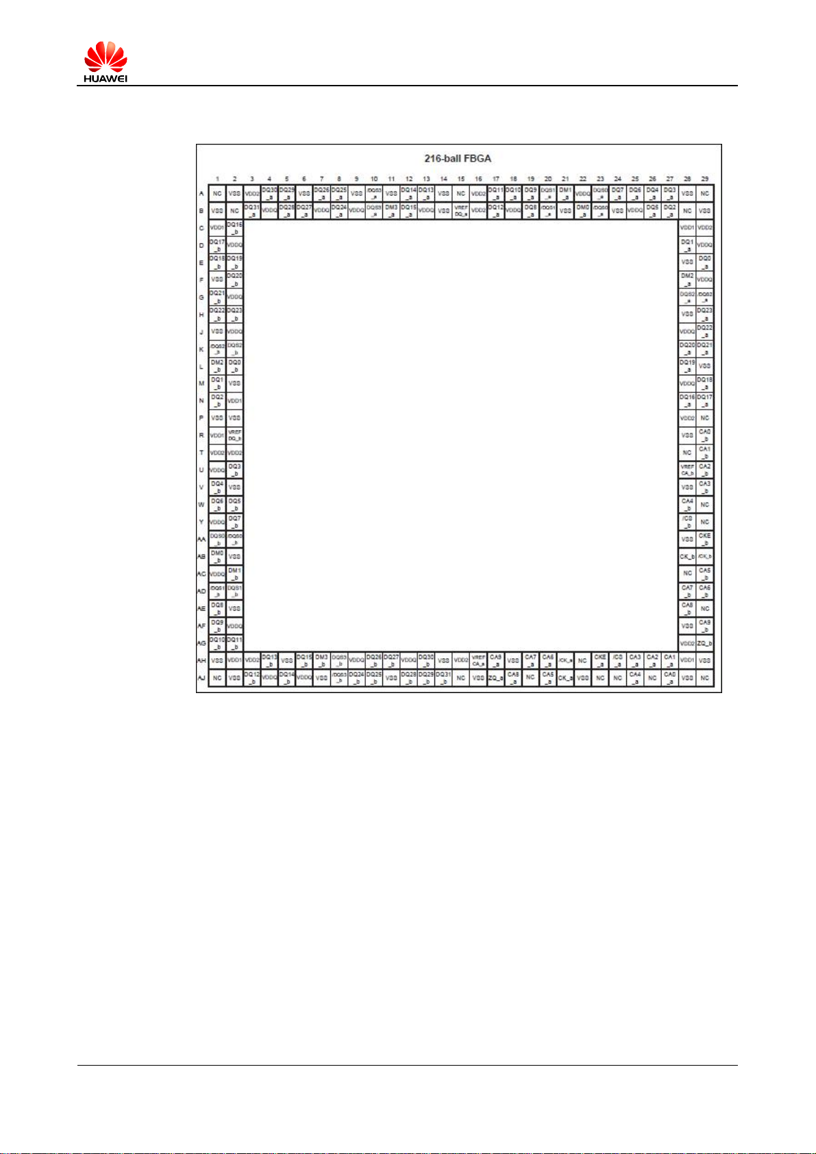
MediaPad10 FHD Maintenance Manual INTERNAL
Figure 2-5 Pin assignment of the POP LPDDR2 chip
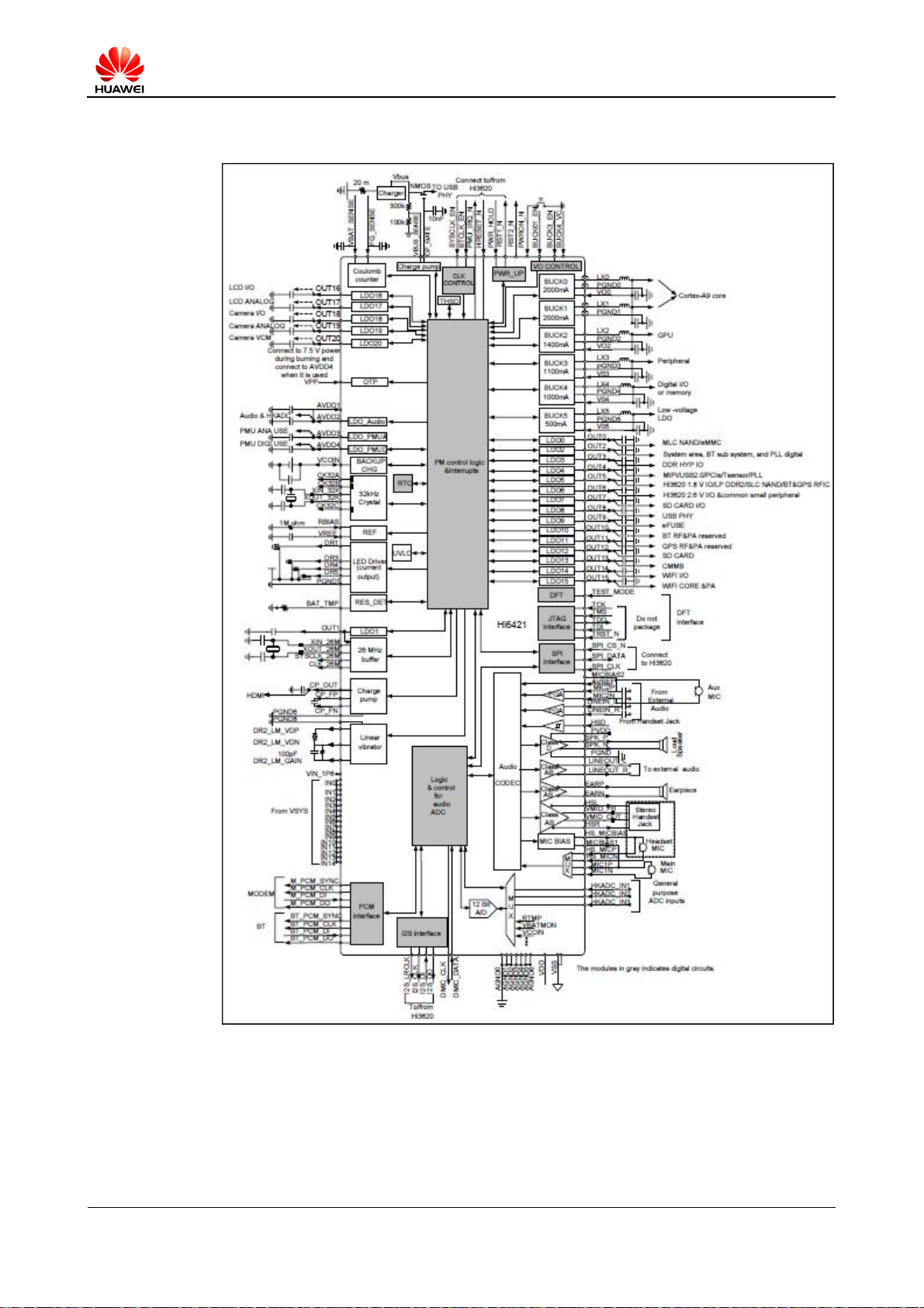
2.3 PMU Hi6421
The Hi6421V200 chip is an important component of Hisilicon K3 application processor
solution, which is a semiconductor solution for mobile phones. It is an integrated circuit that
provides power management, audio processing, and diversified interfaces. Its functions are
described as follows:
Power Supply
BUCK0 and BUCK1 serve as the primary power of the quad core A9, and output 1.1 V by
default. The maximum parallel output current is 4000 mA. BUCK0 and BUCK1 are switched
on or off by controlling the external hardwire signal BUCK01_EN. The output voltage is
adjusted through SPI interfaces to meet the system AVS policy, so that the power consumption
of the system is minimized on the precondition of guaranteed system performance.
2012-10-09 Huawei Confidential Page 20 of 78

MediaPad10 FHD Maintenance Manual INTERNAL
BUCK2 serves as the primary power of the GPU, and outputs 1.1 V by default. Its maximum
current is 1400 mA. SPI interfaces are applied to switch on or off BUCK2 and adjust the
output voltage of BUCK2, so that the power consumption of the system is effectively
controlled.
BUCK3 supplies power to the peripherals of the Hi3620, and outputs 1.1 V by default. Its
maximum current is 1100 mA. BUCK3 is switched on or off by controlling the external
hardwire signal BUCK3_EN.
BUCK4 supplies power to the I/O of the Hi3620 (by default the power voltage is 1.8 V) or the
LP DDR2 (by default the power voltage is 1.2 V). Its maximum current is 1000 mA. The
default output voltage varies according to different applications. The default output voltage is
controlled by the external hardwire signal BUCK4_VC.
BUCK5 serves as the input power of LDO2 and LDO3 to improve the operating efficiency of
low dropout (LDO) regulators. Its maximum current is 500 mA.
Of the 24 LDOs, 21 LDOs supply power to the following components:
l
MLC NAND
l
26 MHz clock oscillation circuit
l
AP system area
l
DDR HPY I/O
l
MIPI
l
3620 and Hi6421V200 digital I/O
l
3620 2.6 V I/O
l
microSD card I/O
l
USB PHY
l
eFuse
l
Bluetooth
l
GPS
l
microSD card
l
CMMB
l
Wi-Fi I/O
l
Wi-Fi core
l
LCD I/O
l
LCD analog
l
Camera I/O
l
Camera analog
l
Camera VCM
All these power channels support power saving (in dormant or ECO mode). The rest three
LDOs supply power to an audio circuit (including HKADC), a PMU analog circuit, and a
PMU digital circuit. The charge pump supplies power to the HDMI, and provides the backup
battery charging function.
Audio Unit
The audio unit integrates a sigma-delta audio codec, which makes possible flexible resource
configuration and provides abundant audio applications to meet audio processing
2012-10-09 Huawei Confidential Page 21 of 78

MediaPad10 FHD Maintenance Manual INTERNAL
Interface Unit
requirements in various scenarios. The Hi6421V200 chip can connect to the AP, modem, or
Bluetooth through one I2S interface and two PCM digital audio interfaces. It can also connect
to peripherals through analog interfaces, such as line I/O and MIC interfaces.
Furthermore, the audio unit implements interworking and switching between audio signal
resources, provides sound volume adjustment, and supports digital MIC input signals.
Multiple audio amplifiers are built in the Hi6421V200 chip to drive the loudspeaker, headset,
and earpiece. The headset checking function is used to identify whether the headset is
installed. It helps the system save power overheads, and supports headset key detection.
The interface unit of the Hi6421V200 chip provides the following functions:
l
Uses SPI interfaces to implement high-rate communication with the AP
l
Provides a coulometer to detect changes to the electric energy of the battery
l
Provides a 12-bit HKADC to monitor four channels of analog parameters in real time,
including the voltage of the main battery, the temperature of the main battery, and the
voltage of the backup coin battery.
l
Provides the drive for one vibration motor or linear motor, one LED background drive
(maximum current 40 mA), and three LED drives (the breathing function can be
configured)
l
Provides one 26 MHz clock oscillator and two output drives.
l
Provides one 32.768 kHz clock oscillator and three output drives.
l
Provides one interface circuit for detecting the thermistor of the main battery.
Figure 2-6 shows the functional blocks of the power supply.
2012-10-09 Huawei Confidential Page 22 of 78
MediaPad10 FHD Maintenance Manual INTERNAL
Figure 2-6 Functional blocks of the power supply
The Hi6421V200 chip has the following features:
l
Five high-efficiency buck-type switch power convertors
BUCK0: 1.1 V 2000 mA for the A9 Core, supporting AVS adjustment.
BUCK1: 1.1 V 2000 mA for the A9 Core, supporting AVS adjustment.
2012-10-09 Huawei Confidential Page 23 of 78

MediaPad10 FHD Maintenance Manual INTERNAL
BUCK2: 1.1 V 1400 mA for the GPU, supporting AVS adjustment.
BUCK3: 1.1 V 1100 mA for peripherals.
BUCK4: 1.2 V or 1.8 V 1000 mA for LPDDR2 or AP I/O.
BUCK5: 1.8 V 500 mA for low-voltage LDO.
BUCK0 and BUCK1 are connected in parallel.
l
21 external LDO linear voltage regulators and four internal LDO linear voltage
regulators
LDO0: 2.85 V @ 300 mA for MLC NAND/eMMC
LDO1: 1.8 V @ 50 mA for 26 MHz clock oscillation circuit
LDO2: 1.1 V @ 150 mA for the system area, Bluetooth subsystem, and digital PLL (The
system in standby mode does not need to be powered off)
LDO3: 1.2 V @ 350 mA for the DDR PHY I/O to be powered off or the HSIC PHY 1.2
V (Power-off is required)
LDO4: 2.5 V @ 250 mA for MIPI/USB2.0/PCIe/T Sensor/PLL 2.5 V analog power
(Power-off is required)
LDO5: 1.8 V @ 300 mA for Hi3620 & Hi6421V200 1.8V I/O, LP DDR2, SLC NAND,
or Bluetooth&GPS RFIC
LDO6: 2.6 V @ 300 mA for Hi3620 2.6 V I/O and small peripherals
LDO7: 2.6 V @ 50 mA for Hi3620 microSD card slot I/O (Dynamic switching between
1.8 V and 2.6 V is needed)
LDO8: 3.3 V @ 200 mA for USB PHY
LDO9: 2.6 V @ 200 mA for eFuse power supply (Power-off is required)
LDO10: 2.85 V @ 150 mA for Bluetooth RF&PA; reserved
LDO11: 2.85 V @ 150 mA for GPS RF&PA; reserved
LDO12: 2.85 V @ 500 mA for the microSD card
LDO13: 2.85 V @ 300 mA for CMMB
LDO14: 2.85 V @ 150 mA for Wi-Fi I/O
LDO15: 3.3 V @ 300 mA for Wi-Fi core&PA
LDO16: 2.85 V @ 150 mA for LCD I/O
LDO17: 2.85 V @ 150 mA for LCD Analog
LDO18: 2.85 V @ 300 mA for Camera I/O and the input of the internal core power
regulator
LDO19: 2.85 V @ 300 mA for LCD Camera Analog
LDO20: 2.85 V @ 300 mA for LCD Camera VCM
LDO_Audio: 3.3 V @ 300 mA for Audio & HKADC
LDO_PMUA: 3.15 V @ 10 mA for PMU Analog
LDO_PMUD: 1.8 V @ 10 mA for PMU Digital
l
Real-time clock (RTC) with the alarm clock function
The Hi6421V200 chip integrates a 32.768 kHz crystal oscillator and supports three
channels of clock buffer output independently controlled.
The RTC serves as the reference time and date benchmark of the system.
The RTC supports the alarm clock function and scheduled power-on.
The RTC supports power supply through a backup coin battery.
2012-10-09 Huawei Confidential Page 24 of 78
 Loading...