HP IVA-05128 Datasheet

Silicon Bipolar MMIC 1.5 GHz
Variable Gain Amplifier
Technical Data
IVA-05128
Features
28 Package
• 50 MHz to 1.5 GHz
Bandwidth
• Data Rates up to 2.0 Gbit/s
• High Gain: 26 dB Typical
• Wide Gain Control Range:
30␣ dB Typical
• Differential Output
Capability
• Bias V
• 5 V TTL Compatible V
Control Voltage, l
- Vee = 5 V
CC
< 3 mA
gc
gc
• Hermetic Ceramic Surface
Mount Package
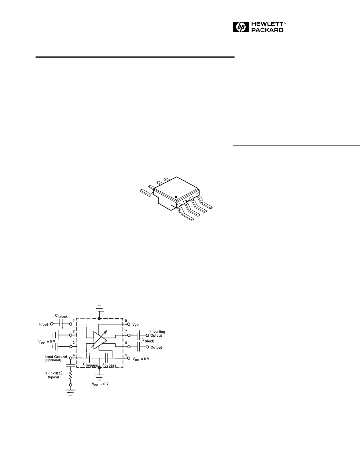
Typical Biasing Configuration and
Functional␣ Block␣ Diagram
PIN 1
Description
The IVA-05128 is a variable gain
amplifier housed in a miniature
ceramic hermetic surface mount
package. It is designed for narrow
or wide bandwidth commercial,
industrial and military
applications that require high gain
and wide gain control range. The
amplifier can be used in a singleended or differential output
configuration. For low frequency
applications (<50 MHz) a bypass
capacitor and series resistor are
connected to pin 4, the AC Input
Ground lead.
Typical applications include
variable gain amplification for
fiberoptic systems at data rates in
excess of the 1.24 Gb/s SONET
standard, mobile radio and
satellite receivers, millimeter
wave receiver IF amplifiers and
communications receivers.
6-173
The IVA series of variable gain
amplifiers is fabricated using HP’s
10 GHz fT, 25 GHz f
silicon bipolar process. This
process uses nitride selfalignment, submicrometer
lithography, trench isolation, ion
implantation, gold metallization
and polyimide inter-metal
dielectric and scratch protection
to achieve excellent performance,
uniformity and reliability.
ISOSATTM-I
MAX
5965-9974E

Absolute Maximum Ratings
Parameter Maximum
Device Voltage 8 V
Power Dissipation
Input Power +14 dBm
Vgc - V
ee
Junction Temperature 200°C
Storage Temperature -65°C to 200°C
[2,3]
Absolute
600 mW
7 V
[1]
Thermal Resistance:
[2,4]
θjc = 50°C/W
Notes:
1. Permanent damage may occur if any of
these limits are exceeded.
2. T
= 25°C.
CASE
3. Derate at 20 mW/°C for TC >170°C.
4. See MEASUREMENTS section
"’Thermal Resistance” in
Communications Components Catalog,
for more information.
[2]
[3]
[1]
, T
= 25° C
A
[2]
:
= 50 Ω Units Min. Typ. Max.
O
f = 0.5 GHz dB 20 26
G Hz 1.0 1.5
[4]
[2]
) f = 0.5 GHz, Vgc = 0 to 5 V dB 45
f = 0.5 GHz, Vgc = 0 to 5 V dB 25 30
Electrical Specifications
Parameters and Test Conditions
Symbol VCC = 5 V, Vee = 0 V, Vgc = 0 V, Z
G
∆G
f
3dB
GCR Gain Control Range
ISO Reverse Isolation (|S12|
VSWR
Power Gain |S21|
P
Gain Flatness f = 0.05 to 1.0 GHz dB ±0.3
P
3 dB Bandwidth
Input VSWR f = 0.05 to 1.5 GHz, Vgc = 0 t o 5 V 1.7:1
Output VSWR f = 0.05 to 1.5 GHz, Vgc = 0 t o 5 V 1.5:1
NF 50 Ω Noise Figure f = 0.5 GHz dB 9
P
1dB
Output Power f = 0.5 GHz dBm -2
at 1 dB Compression
IP
Output Third Order f = 0.5 GHz dBm 8
3
Intercept Point
t
I
CC
Notes:
1. The recommended operating voltage range for this device is 4 to 6 V. Typical performance as a function of voltage is on the following
page.
2. As measured using Input Pin 1 and Output Pin 6; with Output Pin 7 terminated into 50 ohms.
3. Referenced from 50 MHz Gain.
4. The recommended gain control range for these devices for dynamic control is 0 to 4.2 V. Operation at gain control settings above 4.2 V
may result in gain increase rather than gain decrease.
Group Delay f = 0.5 GHz psec 400
D
Supply Current mA 25 35 45
6-174
 Loading...