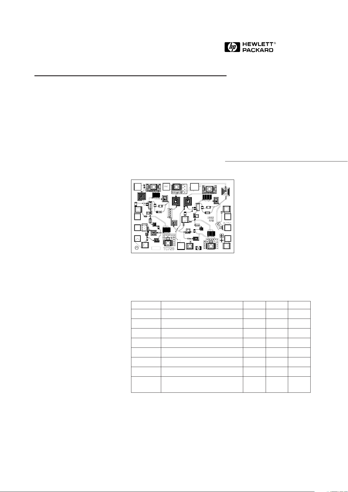
HP HMMC-5620DC, HMMC-5620RF Datasheet

6-70
6 – 20 GHz High-Gain Amplifier
Technical Data
Features
• Wide-Frequency Range:
6 – 20 GHz
• High Gain: 17 dB
• Gain Flatness: ± 1.0 dB
• Return Loss:
Input -15 dB
Output -15 dB
• Single Bias Supply
Operation
• Low DC Power Dissipation:
PDC ~ 0.5 Watts
• Medium Power:
20 GHz: P
-1dB
: 12 dBm
P
sat
: 13 dBm
Description
The HMMC-5620 is a wideband
GaAs MMIC Amplifier designed
for medium output power and
high gain over the 6 to 20 GHz
frequency range. Four MESFET
cascade stages provide high gain,
while the single bias supply offers
ease of use. E-Beam lithography
is used to produce gate lengths of
≈ 0.3 µm. The HMMC-5620 incor-
porates advanced MBE technology, Ti-Pt-Au gate metallization,
silicon nitride passivation, and
polyimide for scratch protection.
Absolute Maximum Ratings
[1]
Symbol Parameters/Conditions Units Min. Max.
V
DD
Positive Drain Voltage V 7.5
I
DD
Total Drain Current mA 135
P
DC
DC Power Dissipation watts 1.0
P
in
CW Input Power dBm 20
T
ch
Operating Channel Temp. °C +160
T
case
Operating Case Temp. °C -55
T
STG
Storage Temperature °C - 65 +165
T
max
Maximum Assembly Temp. °C +300
(for 60 seconds maximum)
Notes:
1. Operation in excess of any one of these conditions may result in permanent
damage to this device. T
A
= 25°C except for T
ch
, T
STG
, and T
max
.
Chip Size: 1410 x 1010 µm (55.5 x 39.7 mils)
Chip Size Tolerance: ± 10 µm (± 0.4 mils)
Chip Thickness: 127 ± 15 µm (5.0 ± 0.6 mils)
Pad Dimensions: 80 x 80 µm (2.95 x 2.95 mils), or larger
HMMC-5620
5965-5442E

6-71
HMMC-5620 DC Specifications/Physical Properties
[1]
Symbol Parameters and Test Conditions Units Min. Typ. Max.
I
DD
Drain Current (VDD = +5.0 V) mA 70 100 135
I
DD
Drain Current (VDD = +7.0 V) mA 105
θ
ch-bs
Thermal Resistance (T
backside
= 25° C) °C/W 70
Note:
1. Measured in wafer form with T
chuck
= 25°C. (Except θ
ch-bs
).
HMMC-5620 RF Specifications/Physical Properties
VDD = 5.0 V, IDD(Q) = 100 mA, Zin =Z
o
= 50 Ω
[1]
Symbol Parameters and Test Conditions Units Min. Typ. Max.
BW Guaranteed Bandwidth GHz 6 20
S
21
Small Signal Gain dB 15 17 21
∆S
21
Small Signal Gain Flatness dB ±1.0 ± 1.25
RL
in
Input Return Loss dB -15 -10
RL
out
Output Return Loss dB -15 -10
S
12
Reverse Isolation dB -55
P
-1dB
Output Power @ 1 dB Gain Compression dBm 12
P
sat
Saturated Output Power dBm 13
H
2
Second Harmonic Power Level (6 < ƒo < 20) dBc -30
Po(ƒo) = 10 dBm
H
3
Third Harmonic Power Level (6 < ƒo < 20) dBc -40
Po(ƒo) = 10 dBm
NF Noise Figure dB 9.0
Note:
1. Small-signal data measured in wafer form with T
chuck
= 25°C. Large-signal data measured on individual devices
mounted in an HP83040 Series Modular Microcircuit Package at T
A
= 25°C.
 Loading...