6-64
6 –20 GHz Amplifier
Technical Data
Features
• High Efficiency:
11% @ P
-1dB
Typical
• Output Power, P
-1dB
:
18 dBm Typical
• High Gain: 14 dB Typical
• Flat Gain Response:
± 0.5 dB Typical
• Low Input/Output VSWR:
<1.7:1 Typical
• Single Supply Bias:
5 volts (@ 115 mA Typical)
with Optional Gate Bias
Description
The HMMC-5618 6–20 GHz MMIC
is an efficient two-stage amplifier
that is designed to be used as a
cascadable intermediate gain
block for EW applications. In
communication systems, it can be
used as an amplifier for a local
oscillator, or as a transmit
amplifier. It is fabricated using a
PHEMT integrated circuit structure that provides exceptional
efficiency and flat gain performance. During typical operation,
with a single 5-volt DC power
supply, each gain stage is biased
for Class-A operation for optimal
power output with minimal
distortion. The RF input and RF
output has matching circuitry for
use in 50␣ ohm environments.
Absolute Maximum Ratings
[1]
Symbol Parameters/Conditions Units Min. Max.
VD1, V
D2
Drain Supply Voltage V 5.5
V
G1
Optional Gate Supply Voltage V -5 +1
V
G2
Optional Gate Supply Voltage V -10 +1
I
D1
Drain Supply Current mA 70
I
D2
Drain Supply Current mA 84
P
in
RF Input Power
[2]
dBm 20
T
ch
Channel Temp.
[3]
°C +160
T
A
Backside Ambient Temp. °C -5 5 +100
T
STG
Storage Temperature °C -6 5 +150
T
max
Maximum Assembly Temp. °C +300
Notes:
1. Absolute maximum ratings for continuous operation unless otherwise noted.
2. Operating at this power level for extended (continuous) periods is not
recommended.
3. Refer to DC Specifications/Physical Properties table for derating information.
HMMC-5618
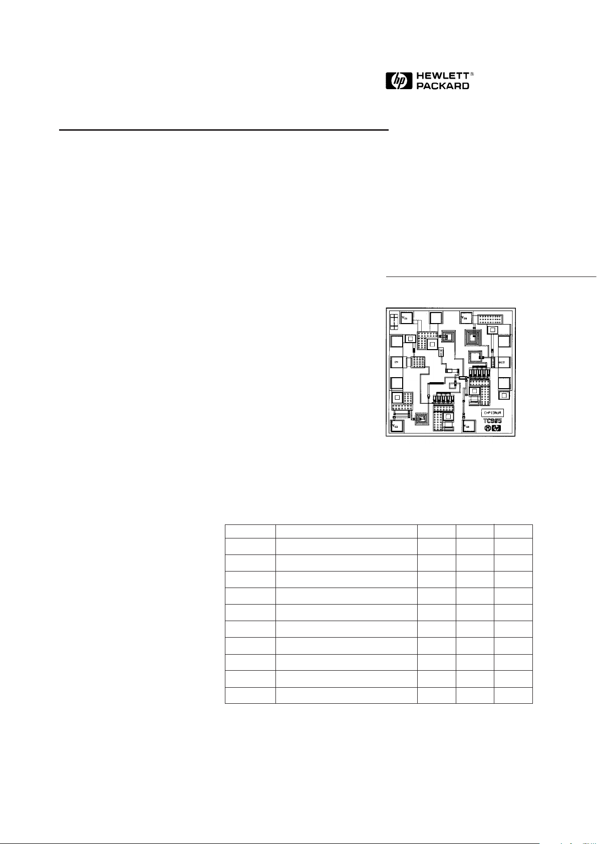
Chip Size: 920 x 920 µm (36.2 x 36.2 mils)
Chip Size Tolerance: ± 10 µm (± 0.4 mils)
Chip Thickness: 127 ± 15 µm (5.0 ± 0.6 mils)
Pad Dimensions: 80 x 80 µm (3.2 x 3.2 mils)
The backside of the chip is both
RF and DC ground. This helps
simplify the assembly process
and reduces assembly related
performance variations and costs.
The MMIC is a cost effective
alternative to hybrid (discreteFET) amplifiers that require
complex tuning and assembly
processes.
6-64
5965-5443E

6-65
HMMC-5618 DC Specifications/Physical Properties
[1]
Symbol Parameters and Test Conditions Units Min. Typ. Max.
VD1, V
D2
Drain Supply Voltage V 3.0 5.0 5.5
I
D1
Stage-One Drain Supply Current mA 50
(VD1 = 5 V , VG1 = Open or Ground)
I
D2
Stage-Two Drain Supply Current mA 65
(VD2 = 5 V , VG2 = Open or Ground)
ID1 + I
D2
Total Drain Supply Current mA 115 140
(VD1 = VD2 = 5 V, VG1 = VG2 = Open or Ground)
V
P1
Optional Input-Stage Gate Supply Pinch-off Voltage V -4 -2.8
(VD1 = 5 V , ID1 < 3 mA: Input Stage OFF
[2]
)
I
G1
Gate Supply Current (Input Stage OFF
[2]
) m A 0.9
V
P2
Optional Input-Stage Gate Supply Pinch-off Voltage V -7.5 -5.3
(VD2 = 5 V , ID2 < 3.6 mA: Output Stage OFF
[2]
)
I
G2
Gate Supply Current (Output Stage OFF
[2]
) m A 1.7
(VD2 = 5 V , VG2 = Open or Ground)
θ
ch-bs
Thermal Resistance
[3]
° C/Watt 87
(Channel-to-Backside at T
ch
= 150° C)
T
ch
Channel Temperature
[4]
(T
A
= 100° C, MTTF = 106 hrs, °C 150
V
D1
= VD2 = 5 V, V
G1
= VG2 = Open)
Notes:
1. Backside ambient operating temperature T
A
= 25°C unless otherwise noted.
2. The specified FET stage is in the OFF state when biased with a gate voltage level that is sufficient to pinch off the drain
current.
3. Thermal resistance (in °C/Watt) at a channel temperature T (°C) can be estimated using his equation:
θ(T) ≅ 87 x [T(°C)+ 273] / [150°C + 273].
4. Derate MTTF by a factor of two for every 8°C above T
ch
.
HMMC-5618 RF Specifications, T
A
= 25°C, V
D1
= V
D2
= 5 V, VG1 = V
G2
= Open or Ground, Z
O
= 50 Ω
6–18 GHz 5.9–20 GHz
Symbol Parameters and Test Conditions Units Typ. Min. Max. Min. Max.
Gain Small Signal Gain dB 14 12 11.5
∆ Gain Gain Flatness dB ±0.5
∆S21/∆T Temperature Coefficient of Gain dB/°C -0.025
(RLin)
MIN
Minimum Input Return Loss dB 12 10 9
(RL
out)MIN
Minimum Output Return Loss dB 12 10 10
Isolation Reverse Isolation dB 40
P
-1dB
Output Power @ 1 dB Gain Compression dBm 18 17 17
P
sat
Saturated Output Power (Pin = 10 dBm) dBm 20 18.5 18.5
NF Noise Figure dB 5.5 7 7
 Loading...