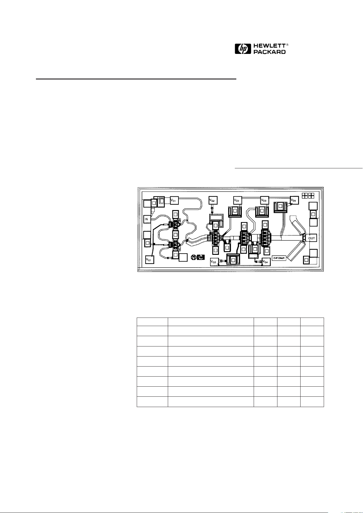
HP HMMC-5040DC, HMMC-5040RF Datasheet

6-58
20 – 40 GHz Amplifier
Technical Data
Features
• Large Bandwidth:
20 - 44 GHz Typical
21 - 40 GHz Specified
• High Gain: 22 dB Typical
• Saturated Output Power:
21 dBm Typical
• Supply Bias:
≤ 4.5 volts @ ≤ 300 mA
Description
The HMMC-5040 is a high-gain
broadband MMIC amplifier
designed for both military applications and commercial communication systems. This four stage
amplifier has input and output
matching circuitry for use in
50␣ ohm environments. It is
fabricated using a PHEMT
integrated circuit structure that
provides exceptional broadband
performance. The backside of the
chip is both RF and DC ground.
This helps simplify the assembly
process and reduces assembly
related performance variations
and costs. This MMIC is a cost
effective alternative to hybrid
(discrete-FET) amplifiers that
require complex tuning and
assembly processes.
HMMC-5040
Absolute Maximum Ratings
[1]
Symbol Parameters/Conditions Units Min. Max.
V
D1, 2-3-4
Drain Supply Voltages V 5
V
G1, 2-3-4
Gate Supply Voltages V -3.0 0.5
I
DD
Total Drain Current mA 400
P
in
RF Input Power dBm 21
T
ch
Channel Temperature
[2]
°C +160
T
A
Backside Ambient Temp. °C -55 +75
T
STG
Storage Temperature °C -6 5 +165
T
max
Maximum Assembly Temp. °C +300
Note:
1. Absolute maximum ratings for continuous operation unless otherwise noted.
2. Refer to DC Specifications/Physical Properties table for derating information.
Chip Size: 1720 x 760 µm (67.7 x 29.9 mils)
Chip Size Tolerance: ± 10 µm (± 0.4 mils)
Chip Thickness: 127 ± 15 µm (5.0 ± 0.6 mils)
Pad Dimensions: 80 x 80 µm (3.1 x 3.1 mils)
5965-5444E

6-59
HMMC-5040 DC Specifications/Physical Properties
[1]
Symbol Parameters and Test Conditions Units Min. Typ. Max.
V
D1, 2-3-4
Drain Supply Operating Voltages V 2 4.5 5
I
D1
First Stage Drain Supply Current mA 55
(VDD = 4.5 V, VG1 = -0.6 V)
I
D2-3-4
Total Drain Supply Current for Stages 2, 3, and 4 mA 24.5
(VDD = 4.5 V, VGG = -0.6 V)
V
G1, 2, 3-4
Gate Supply Operating Voltages (IDD = 300 mA) V -0.6
V
p
Pinch-off Voltage (VDD = 4.5 V, I
DD
≤ 1 0 mA) V -2 -1.2 -0.8
θ
ch-bs
Thermal Resistance
[2]
°C/W 62
(Channel-to-Backside @ T
ch
= 160° C)
T
ch
Channel Temperature
[3]
(T
A
= 125° C, MTTF > 106 hrs, °C 160
VDD = 4.5 V, IDD = 300 mA)
Notes:
1. Backside ambient operating temperature T
A
= 25°C unless otherwise noted.
2. Thermal resistance (°C/Watt) at a channel temperature T (°C) can be estimated using the equation:
θ(T) ≅ 62 x [T(°C)+ 273] / [160° C + 273].
3. Derate MTTF by a factor of two for every 8°C above T
ch
.
HMMC-5040 RF Specifications, T
A
= 25° C, V
DD
= 4.5 V, IDD = 300 mA, Z
o
= 50 Ω
Broadband Narrow Band
Symbol Parameters/Conditions Specifications Performance
Units Min. Typ. Max. Typical
BW Operating Bandwidth GHz 21 20–44 40 21–24 27–29 37–40
S
21
Small Signal Gain dB 20 22 25 23 22
∆ S
21
Small Signal Gain Flatness dB ±1.5 ±1 ± 0.75 ± 0.3
(RLin)
MIN
Minimum Input Return Loss dB 8 10 9 10 14
(RL
out)MIN
Minimum Output Return Loss dB 8 10 10 11 12
S
12
Reverse Isolation dB 54 54 54 54
P
-1dB
Output Power dBm 18 18 18 18
(@ 1dB Gain Compression)
P
sat
Saturated Output Power dBm 20 21 21 21 21
@ 3 dB Gain Compression
 Loading...