HP HMMC-5038DC, HMMC-5038RF Datasheet

6-53
38 GHz LNA
Technical Data
Features
• Low Noise Figure: 4.8 dB
• Frequency Range:
37␣ –␣ 40␣ GHz
• High Gain (Adjustable):
3 V, 120 mA @ 23 dB Gain
3 V, 80 mA @ 20 dB Gain
• 50 Ω Input/Output Matching
Description
The HMMC-5038 MMIC is a highgain low-noise amplifier (LNA)
designed for communication
receivers that operate from
37␣ GHz to 40 GHz. The gain of
this four stage LNA can be
adjusted by altering the gate bias
of the output two, or three, stages
while maintaining optimum noise
figure bias for the input stage(s).
Large FETs provide high power
handing capability to avoid power
compression. The backside of the
chip is both RF and DC ground.
This helps simplify the assembly
process and reduce assembly
related performance variations
and costs.
The HMMC-5038 is fabricated
using a PHEMT integrated
circuit structure that provides
good noise and gain performance.
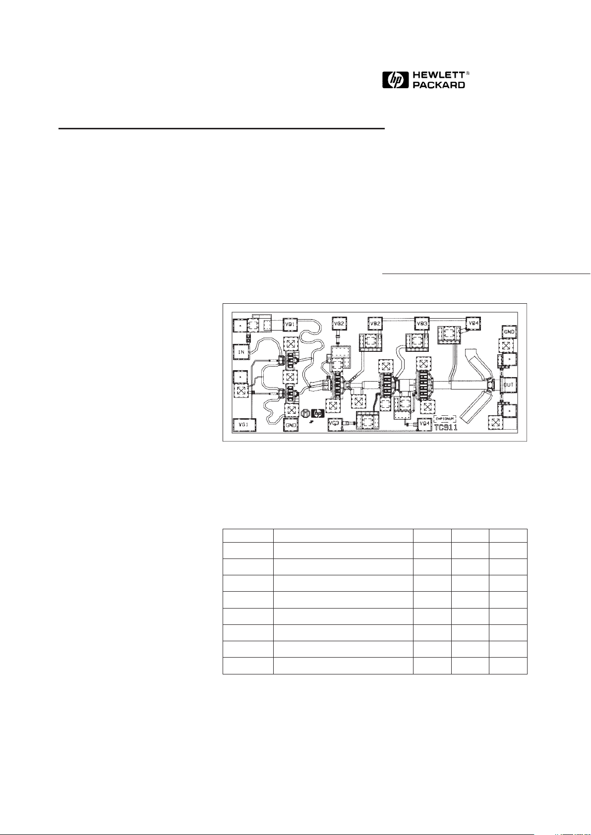
Chip Size: 1630 x 760 µm (64.2 x 29.9 mils)
Chip Size Tolerance: ± 10 µm (± 0.4 mils)
Chip Thickness: 127 ± 15 µm (5.0 ± 0.6 mils)
Pad Dimensions: 80 x 80 µm (3.1 x 3.1 mils)
HMMC-5038
Absolute Maximum Ratings
[1]
Symbol Parameters/Conditions Units Min. Max.
V
D1, 2-3-4
Drain Supply Voltages V 5
I
G1, 2-3-4
Gate Supply Voltages V -3.0 0
I
DD
Total Drain Current mA 300
P
in
RF Input Power dBm 15
T
ch
Channel Temperature
[2]
°C +160
T
A
Backside Ambient Temp. °C -5 5 +125
T
STG
Storage Temperature °C -6 5 +165
T
max
Maximum Assembly Temp. °C +310
Note:
1. Absolute maximum ratings for continuous operation unless otherwise noted.
2. Refer to DC Specifications/Physical Properties table for derating information.
5965-5445E

6-54
DC Specifications/Physical Properties
[1]
Symbol Parameters and Test Conditions Units Min. Typ. Max.
V
D1, 2-3-4
Low Noise Drain Supply Operating Voltages V 2 3 5
I
D1
First Stage Drain Supply Current mA 22
(VDD = 3 V, VG1 = -0.8 V)
I
D2-3-4
Drain Supply Current for Stages 2, 3, and 4 Combined mA 98
(VDD = 3 V, VGG = -0.8 V)
V
G1, 2, 3-4
Gate Supply Operating Voltages (IDD = 120 mA) V -0.8
V
p
Pinch-off Voltage (VDD = 3 V, I
DD
≤ 10 mA) V -2 -1.2 -0.8
θ
ch-bs
Thermal Resistance
[2]
°C/W 62
(Channel-to-Backside @ T
ch
= 160° C)
T
ch
Channel Temperature
[3]
(T
A
= 125° C, MTTF > 106 hrs, °C 150
VDD = 3 V, IDD = 120 mA)
Notes:
1. Backside ambient operating temperature T
A
= 25°C unless otherwise noted.
2. Thermal resistance (°C/Watt) at a channel temperature T (°C) can be estimated using the equation:
θ(T) ≅ 62 x [T(°C)+ 273] / [160° C + 273].
3. Derate MTTF by a factor of two for every 8°C above T
ch
.
RF Specifications, T
A
= 25° C, V
DD
= 3 V, IDD = 120 mA, Z
o
= 50 Ω
Symbol Parameters and Test Conditions Units Min. Typ. Max.
BW Operating Bandwidth GHz 37 40
S
21
Small Signal Gain
[1]
d B 20 23
∆ S
21
Small Signal Gain Flatness dB ±0.5
(RLin)
MIN
Minimum Input Return Loss w/o external dB 8 12
capacitive matching
[2]
(RL
out)MIN
Minimum Output Return Loss dB 12 18
S
12
Reverse Isolation dB 50
P
-1dB
Output Power @ 1dB Gain Compression dBm 12
NF Noise Figure
[3]
d B 4.8
Notes:
1. Gain may be reduced by biasing for lower IDD. Increasing IDD will increase Gain.
2. Minimum input return may be improved by approximately 3 dB by including a small capacitive (~30 fF) stub on the
input transmission line.
3. Noise Figure may be further reduced by optimizing DC bias conditions.
 Loading...