6-47
H
2 – 26.5 Medium Power Amplifier
Technical Data
Features
• Wide-Frequency Range:
2 - 26.5 GHz
• Moderate Gain: 7 dB
• Gain Flatness: 1 dB
• Return Loss:
Input -13 dB
Output -11 dB
• Low-Frequency Operation
Capability: < 2 GHz
• Gain Control:
30 dB Dynamic Range
• Medium Power:
20 GHz: P
-1dB
: 22 dBm
P
sat
: 24 dBm
26.5 GHz: P
-1dB
: 19 dBm
P
sat
: 21 dBm
Description
The HMMC-5027 is a broadband
GaAs MMIC Traveling Wave
Amplifier designed for medium
output power and moderate gain
over the full 2 to 26.5 GHz
frequency range. Seven MESFET
cascode stages provide a flat gain
response, making the HMMC-5027
an ideal wideband power block.
Optical lithography is used to
produce gate lengths of ≈ 0.5 mm.
The HMMC-5027 incorporates
advanced MBE technology,
Ti-Pt-Au gate metallization,
silicon nitride passivation, and
polyimide for scratch protection.
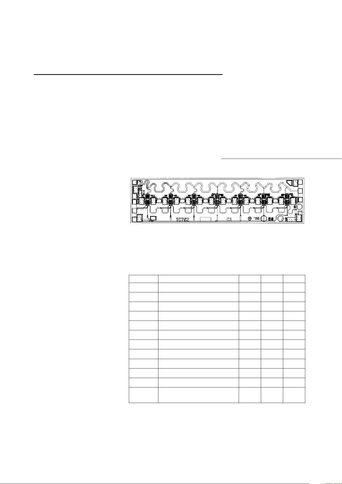
Chip Size: 2980 x 770 µm (117.3 x 30.3 mils)
Chip Size Tolerance: ± 10 µ m (± 0.4 mils)
Chip Thickness: 127 ± 15 µm (5.0 ± 0.6 mils)
Pad Dimensions: 75 x 75 µm (2.95 x 2.95 mils), or larger
HMMC-5027
Absolute Maximum Ratings
[1]
Symbol Parameters/Conditions Units Min. Max.
V
DD
Positive Drain Voltage V 8.0
I
DD
Total Drain Current mA 300
V
G1
First Gate Voltage V -5 0
I
G1
First Gate Current mA -1 +1
V
G2
Second Gate Voltage V -2.5 +5
I
G2
Second Gate Current mA -25
P
DC
DC Power Dissipation watts 2.4
P
in
CW Input Power dBm 23
T
ch
Operating Channel Temp. °C +150
T
case
Operating Case Temp. °C -55
T
STG
Storage Temperature °C -6 5 +165
T
max
Maximum Assembly Temp.
°C +300
(for 60 seconds maximum)
Note:
1. Operation in excess of any one of these conditions may result in permanent
damage to this device. T
A
= 25° C except for T
ch
, T
STG
, and T
max
.
5965-5447E

6-48
HMMC-5027 DC Specifications/Physical Properties
[1]
Symbol Parameters and Test Conditions Units Min. Typ. Max.
I
DSS
Saturated Drain Current mA 200 300 500
(VDD = 8.0 V, VG1 = 0.0 V, VG2 = open circuit)
V
p
First Gate Pinch-off Voltage V -2.2 -1.3 -.5
(VDD = 8.0 V, IDD = 30 mA, VG2 = open circuit)
V
G2
Second Gate Self-Bias Voltage V 1.8
(VDD = 8.0 V, VG1 = 0.0 V) (0.27 x V
DD
)
I
DSOFF(VG1
) First Gate Pinch-off Current mA 7
(VDD = 8.0 V, VG1 = -3.5 V, VG2 = open circuit)
I
DSOFF(VG2
) Second Gate Pinch-off Current mA 10
(VDD = 5.0 V, VG1 = 0.0 V, VG2 = -3.5 V)
θ
ch-bs
Thermal Resistance (T
backside
= 25° C) °C/W 28
Note:
1. Measured in wafer form with T
chuck
= 25°C. (Except θ
ch-bs
.)
HMMC-5027 RF Specifications
[1]
,
T
op
= 25°C, V
D1
= V
D2
= 5 V, VG1 = VG2= Open, Z
O
= 50 Ω, unless otherwise noted
Symbol Parameters and Test Conditions Units Min. Typ. Max.
BW Guaranteed Bandwidth
[2]
GH z 2 26.5
S
21
Small Signal Gain dB 6 7
∆ S
21
Small Signal Gain Flatness dB ±0.8
RL
in
Input Return Loss dB -13 -10
RL
out
Output Return Loss dB -11 -10
S
12
Reverse Isolation dB -28 -25
P
-1dB
Output Power @ 1dB Gain Compression dBm 16.5 19
P
sat
Saturated Output Power dBm 18.5 21
H
2
Second Harmonic Power Level (2 < ƒo < 2 0) dBc -21 -18
[Po(ƒo) = 21 dBm or P
-1dB
, whichever is less]
H
3
Third Harmonic Power Level (2 < ƒo < 2 0) dBc -32 -18
[Po(ƒo) = 21 dBm or P
-1dB
, whichever is less]
NF Noise Figure dB 11
Notes:
1. Small-signal data measured in wafer form with T
chuck
= 25°C. Large-signal data measured on individual devices
mounted in an HP83040 Series Modular Microcircuit Package at T
A
= 25°C.
2. Performance may be extended to lower frequencies through the use of appropriate off-chip circuitry. Upper corner
frequency ~ 30 GHz.
 Loading...