HP HDMP-1014, HDMP-1012 Datasheet

Low Cost Gigabit Rate
Transmit/Receive Chip Set
Technical Data
HDMP-1012 Transmitter
HDMP-1014 Receiver
Features
• Transparent, Extended
Ribbon Cable Replacement
• Implemented in a Low Cost
Aluminum M-Quad 80
Package
• High-Speed Serial Rate 150-
1500 MBaud
• Standard 100K ECL
Interface
16, 17, 20, or 21 Bits Wide
• Reliable Monolithic Silicon
Bipolar Implementation
• On-chip Phase-Locked Loops
- Transmit Clock Generation
- Receive Clock Extraction
Applications
• Backplane/Bus Extender
• Video, Image Acquisition
• Point to Point Data Links
• Implement SCI-FI Standard
• Implement Serial HIPPI
Specification
Description
The HDMP-1012 transmitter and
the HDMP-1014 receiver are used
to build a high speed data link for
point to point communication.
The monolithic silicon bipolar
transmitter chip and receiver chip
are each provided in a standard
aluminum M-Quad 80 package.
From the user’s viewpoint, these
products can be thought of as
providing a “virtual ribbon cable”
interface for the transmission of
data. Parallel data loaded into the
Tx (transmitter) chip is delivered
to the Rx (receiver) chip over a
serial channel, which can be
either a coaxial copper cable or
optical link.
The chip set hides from the user
all the complexity of encoding,
multiplexing, clock extraction,
demultiplexing and decoding.
Unlike other links, the phaselocked-loop clock extraction
circuit also transparently provides
for frame synchronization - the
user is not troubled with the
periodic insertion of frame
synchronization words. In
addition, the dc balance of the
line code is automatically
maintained by the chip set. Thus,
the user can transmit arbitrary
data without restriction. The Rx
chip also includes a state-machine
controller (SMC) that provides a
startup handshake protocol for
the duplex link configuration.
The serial data rate of the T/R link
is selectable in four ranges (see
tables on page 5), and extends
from 120 Mbits/s up to 1.25
Gbits/s. The parallel data interface
is 16 or 20 bit single-ended ECL,
pin selectable. A flag bit is
available and can be used as an
extra 17th or 21st bit under the
user’s control. The flag bit can
also be used as an even or odd
frame indicator for dual-frame
transmission. If not used, the link
performs expanded error
detection.
The serial link is synchronous,
and both frame synchronization
5962-0049E (6/94)
573

and bit synchronization are
maintained. When data is not
available to send, the link
maintains synchronization by
transmitting fill frames. Two
(training) fill frames are reserved
for handshaking during link
startup.
User control space is also supported. If Control Available is
asserted at the Tx chip, the least
significant 14 or 18 bits of the
data are sent and the Rx Control
Available line will indicate the
data as a Control Word.
It is the intention of this data
sheet to provide the design
engineer all of the information
regarding the HDMP-1012/1014
chipset necessary to design this
product into their application. To
assist you in using this data sheet,
the following Table of Contents is
provided.
Table of Contents
Topic Page
Typical Applications ....................................................................... 575
Setting the Operating Rate ..............................................................576
Transmitter Block Diagram .............................................................578
Receiver Block Diagram ................................................................. 580
Transmitter Timing Characteristics ................................................ 582
Receiver Timing Characteristics ..................................................... 583
DC Electrical Specifications ........................................................... 584
AC Electrical Specifications ............................................................584
Typical Lock-Up Times ................................................................... 584
Absolute Maximum Ratings ............................................................ 585
Thermal Characteristics ................................................................. 585
I/O Type Definitions ....................................................................... 585
Pin-Out Diagrams .......................................................................... 586
Transmitter Pin Definitions ............................................................ 587
Receiver Pin Definitions ................................................................. 591
Mechanical Dimensions and
Surface Mount Assembly Instructions ......................................... 595
Appendix I: Additional Internal
Architecture Information ........................................................596
Line Code Description .................................................................... 596
Data Frame Codes ......................................................................... 596
Control Frame Codes ..................................................................... 597
Fill Frame Codes ............................................................................ 598
Tx Operation Principles ................................................................. 599
Tx Encoding .................................................................................. 599
Tx Phase Locked Loop ....................................................................600
Rx Operation Principles ................................................................. 601
Rx Encoding ...................................................................................601
HDMP-1014 (Rx) Phase Locked Loop ............................................ 601
HDMP-1014 (Rx) Decoding ............................................................602
HDMP-1014 (Rx) Link Control State
Machine Operation Principle .......................................................603
The State Machine Handshake Protocol ..........................................603
Appendix II: Link Configuration Examples .............................605
Duplex/Simplex Configurations ...................................................... 605
Full Duplex .....................................................................................605
Simplex Method I: Simplex with Low Speed Return Path ...............606
Simplex Method II: Simplex with Periodic Sync Pulse ....................607
Simplex Method III: Simplex with
External Reference Oscillator ......................................................607
Data Interface for Single/Double Frame Mode ................................ 608
Single Frame Mode (MDFSEL=0) .................................................. 608
Double Frame Mode (MDFSEL=1) ................................................ 609
Supply Bypassing and Integrator Capacitor .................................... 610
Integrating Capacitor ......................................................................610
Power Supply Bypassing and Grounding ........................................ 610
Electrical Connections ....................................................................611
I-ECL and O-ECL ............................................................................611
High Speed Interface: I-H50 & O-BLL ............................................612
TTL and Positive 5 V Operation ......................................................613
Mode Options ................................................................................. 614
574
Typical Applications
The HDMP-1012/1014 chipset
was designed for ease of use and
flexibility. This allows the
customer to tailor the use of this
product, through the configuration of the link, based on their
specific system requirements and
application needs. Typical
applications range from
backplane and bus extension to
digital video transmission.
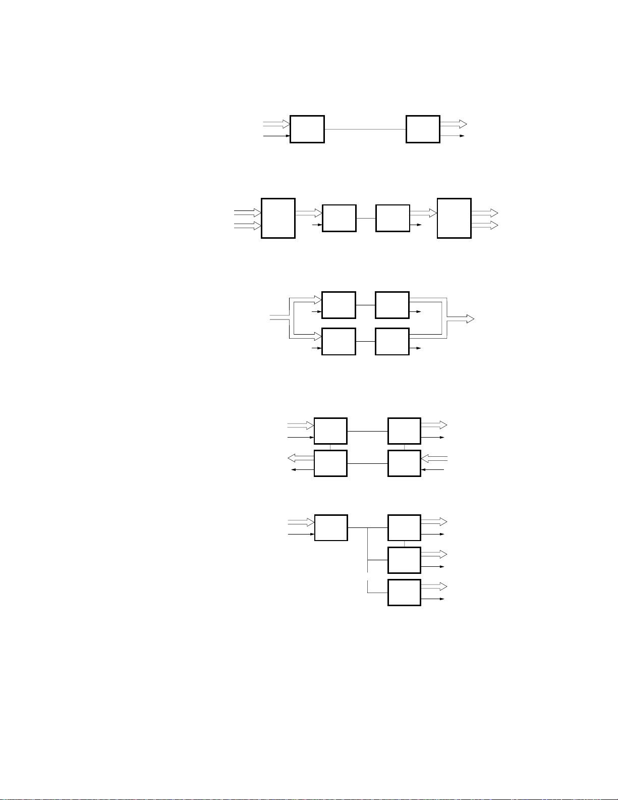
Low latency bus extension of a 16
or 20 bit wide data bus may be
achieved using the standard
duplex configuration (see Figure
1d). In full duplex, the HDMP1012/1014 chipset handles all of
the issues of link startup, maintenance, and simple error
detection.
If the bus width is 32 or 40 bits
wide, the HDMP-1012/1014
chipset is capable of sending the
large data frame as two separate
frame segments, as shown in
Figure 1b. In this mode, called
Double Frame Mode, the FLAG
bit is used by the transmitter and
receiver to indicate the first or
second frame segment. The
HDMP-1012/1014 chipset in
Double Frame Mode may also be
configured in full duplex to
achieve a 32/40 bit wide bus
extension.
For digital video transmission,
simplex links are more common.
The HDMP-1012/1014 chipset
can transmit 16 to 21 bits of
parallel data in standard or
broadcast simplex mode.
Additionally, 32 to 40 bit wide
data can be transmitted over a
single line (in Double Frame
Mode) or two parallel lines, as in
Figure 1c.
CLK CLK
MUX
Tx Rx
A) 16/20 BIT SIMPLEX TRANSMISSION
CLK
CLK
CLK
CLK
CLK
CLK
Tx Rx
B) 32/40 BIT SIMPLEX TRANSMISSION
Tx Rx
Tx Rx
C) 32/40 BIT SIMPLEX TRANSMISSION
WITH HIGH CLOCK RATES
Tx Rx
Rx Tx
D) 16/20 BIT DUPLEX TRANSMISSION
Tx Rx
E) SIMPLEX BROADCAST TRANSMISSION
DEMUX
CLK
CLK
CLK
CLK
CLK
CLK
Rx
.
.
.
.
.
.
.
.
Rx
CLK
CLK
Figure 1. Various Configurations Using the HDMP-1012/1014.
575

For timing diagrams for the
standard configurations, see the
Appendix section entitled Link
Configuration Examples.
The HDMP-1012/1014 chipset can support serial transmission rates from 150 MBd to 1.5 GBd for each of these configurations. The chipset requires the user to input the link data rate by asserting DIV1 and DIV0 accordingly. To determine the DIV1/DIV0 setting necessary for each application, refer to the section: Setting the Operating Data Rate Range on the next page.
Setting the Operating
Data Rate Range
The HDMP-1012/1014 chipset
can operate from 150 MBaud to
1500 MBaud. It is divided into
four operating data ranges with
each range selected by setting
DIV1 and DIV0 as shown in the
tables below.
The purpose of following example
is to help in understanding and
using these tables. This specific
example uses the table in figure 3
entitled “Typical 20-bit Mode Data
Rates”.
It is desired to transmit a 20 bit
parallel word operating at 55 MHz
(55 MWord/sec). Both the Tx and
Rx must be set to a range that this
word rate falls in-between.
According to table entitled
“Typical Operating Rates for 20
Bit Mode” on the next page, a
setting of DIV1/DIV0 = logic ‘0/0’
allows a parallel input word rate
of 32.9 to 62.5 MHz . This setting
easily accommodates the required
55 MHz word rate. The user serial
data rate can be calculated as:
Serial
Data Rate = (––––––) (––––––)
The baud rate includes an
additional 4 bits that G-LINK
transmits for link control and
error detection. The serial baud
rate is calculated as:
Serial
Baud Rate = (––––––) (––––––)
The 55 MHz example is one in
which the parallel word rate
provides only one possible DIV1/
DIV0 setting.
20 bit 55 Mw
word sec
= 1100 MBits/sec
24 bits 55 Mw
word sec
= 1320 MBaud
Some applications may have a
parallel word rate that seems to fit
two ranges. As an example, a 35
MHz (35 MWord/s) parallel data
rate fall within two ranges (DIV0/
DIV1 = 0/0 and DIV0/DIV1 = 0/
1) in 20 Bit Mode. Per the table, a
setting of DIV1/DIV0 = 0/1 gives
an upper rate of 53.3 MHz , while
a setting of DIV1/DIV0 = 0/0
gives a lower rate of 32.9 MHz.
These transition data rates are
stated in the tables as typical
values and may vary between
individual parts. Each transmitter/
receiver has continuous band
cover across its entire 150 to
1500 MBaud range and has
overlap between ranges. Each
transmitter/receiver will permit a
35 MHz parallel data rate, but it is
suggested that DIV0 be a jumper
that can be set either to logic ‘1’
(ground) or logic ‘0’ (open). This
allows the design to accommodate
both ranges for maximum
flexibility. This technique is
recommended whenever
operating near the maximum and
minimum of two word rate
ranges. The above information
also applies to the HDMP-1012/
1014 chipset when operating in
16 bit mode.
576
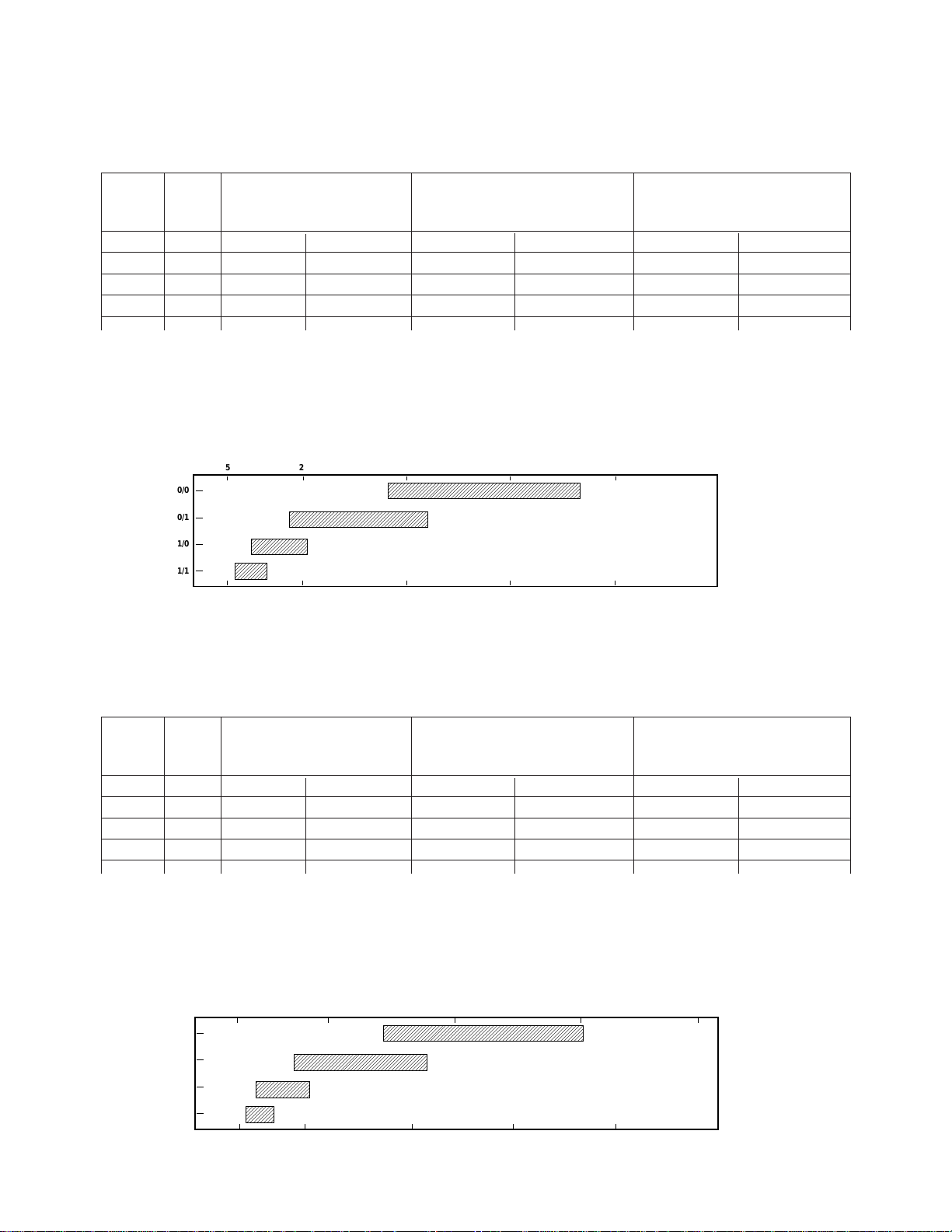
HDMP-1012 (Tx), HDMP-1014 (Rx)
Typical Operating Rates For 16 Bit Mode
Tc = 0°C to +85°C, VEE = -4.5 V to -5.5 V
Parallel Word Rate Serial Data Rate Serial Baud Rate
(Mword/sec) (Mbit/sec) (MBaud)
DIV1 DIV0 Range Range Range
0 0 42 75.0 (max) 672 1200.0 (max) 840 1500.0 (max)
0 1 21 51 336 808 420 1010
1 0 11 25 168 404 210 505
1 1 7.5 (min) 13 120.0 (min) 202 150.0 (min) 253
Notes:
1. Extended operating rates to 1800 MBaud/sec (typ) are possible for Tc = 0°C to +60°C.
2. All values are typical over temperature and process, unless otherwise noted by (min) or (max).
3. Typical Serial Baud Rates for DIV1/DIV0 = 0/0 are up to 1800 MBd.
4. All values in this table are expected for a BER less than 10
which was performed at a serial data rate of 2000 Mbits/s for a BER less than 10
BER = 10-7.
[1]
-14
. This estimation is based on the maximum data rate characterization,
-11
. Production units are 100% screened for less than
FRAME RATE (Mwords/sec)
840
1010
SERIAL DATA RATE (Mbaud)
1800
BAUD RATE = 20 x FRAME RATE
2500200015001000500100
0/0
0/1
1/0
DIV 1 / DIV 0
1/1
5 25 50 75 100 125
420
210
110 253
505
Figure 2: Typical 16-bit Mode Data Rates.
HDMP-1012 (Tx), HDMP-1014 (Rx)
Typical Operating Rates For 20 Bit Mode
Tc = 0°C to +85°C, VEE = -4.5 V to -5.5 V
Parallel Word Rate Serial Data Rate Serial Baud Rate
(Mword/sec) (Mbit/sec) (MBaud/Sec)
DIV1 DIV0 Range Range Range
0 0 35 62.5 (max) 700 1250.0 (max) 840 1500 (max)
0 1 18 42 350 842 420 1010
1 0 9 21 175 421 210 505
1 1 6.3 (min) 10.5 125.0 (min) 211 150 (min) 253
Notes:
1. Extended operating rates to 1800 MBaud/sec are possible for Tc = 0°C to +60°C.
2. All values are typical over temperature and process, unless otherwise noted by (min) or (max).
3. Typical Serial Baud Rates for DIV1/DIV0 = 0/0 are up to 1800 MBd.
4. All values in this table are expected for a BER less than 10
which was performed at a serial data rate of 2000 Mbits/s for a BER less than 10
BER = 10-7.
[1]
-14
. This estimation is based on the maximum data rate characterization,
-11
. Production units are 100% screened for less than
4 25 50 75 100
0/0
0/1
1/0
DIV 1 / DIV 0
1/1
110 253
210
420
505
Figure 3. Typical 20-Bit Mode Data Rates.
FRAME RATE (Mwords/sec)
840
1010
SERIAL DATA RATE (Mbaud)
1800
BAUD RATE = 24 x FRAME RATE
2500200015001000500100
577
RFD
FLAGSEL
M20SEL
STRBIN
EHCLKSEL
DIV0
DIV1
MDFSEL
INPUT
LATCH
ED
FF
CAV*
DAV*
FLAG
D0-D19
RST*
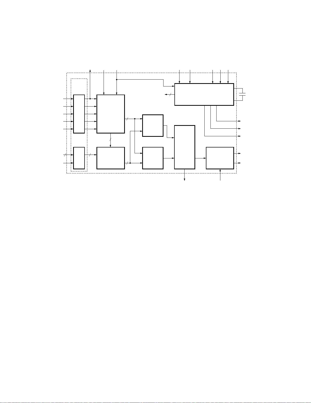
Figure 4. HDMP-1012 Transmitter Block Diagram.
LATCHLATCH
HDMP-1012 Tx Block Diagram
The HDMP-1012 was designed to
accept 16 or 20 bit wide parallel
data and transmit it over a high
speed serial line, while minimizing
the user’s necessary interface to
the high speed circuitry. In order
to accomplish this task, the
HDMP-1012 performs the
following functions:
• Parallel Word Input
• High Speed Clock Multiplication
• Frame Encoding
• Parallel to Serial Multiplexing
CONTROL
LOGIC
+
C-FIELD
ENCODER
D-FIELD
ENCODER
incoming frame clock. The PLL/
Clock Generator locks on to this
incoming rate and multiplies the
clock up to the needed high speed
serial clock. Based on M20SEL,
which determines whether the
incoming data frame is 16 or 20
bits wide, the PLL/Clock
Generator multiplies the frame
rate clock by 20 or 24
respectively (data bits + 4 control
bits). DIV1/DIV0 are set to inform
the transmitter of the frequency
range of the incoming data
frames. The internal frame rate
clock is accessible through
STRBOUT and the high speed
PLL/Clock Generator
The Phase Lock-loop and Clock
serial clock is accessible through
HCLK.
Generator are responsible for
generating all internal clocks
needed by the transmitter to
perform its functions. These
clocks are based on a supplied
frame clock (STRBIN) and control
signals (M20SEL, MDFSEL,
EHCLKSEL, DIV1, DIV0). In
normal operation (MDFSEL=0),
When MDFSEL is set high, the
transmitter is in Double Frame
Mode. Using this option, the user
may send a 32 or 40 bit wide data
frame in two segments while
supplying the original 32 or 40 bit
frame clock at STRBIN. Doubling
of the frame rate is performed by
STRBIN is expected to be the
INTERNAL
CLOCKS
SIGN
FRAME
MUX
PLL / CLOCK
GENERATOR
OUTPUT
ACCUMULATE / INVERT
SELECT
LOOPENINV
the transmitter. The clock
generator section performs the
clock multiplication to the
necessary serial clock rate.
By setting EHCLKSEL high, the
user may provide an external high
speed serial clock at STRBIN.
This clock is used directly by the
high speed serial circuitry to
output the serial data.
Control Logic and C-Field Encoder
The Control Logic is responsible
for determining what information
is serially sent to the output. If
CAV* is low, it sends the data at
D0..D8 and D9..D17 as control
word information. If CAV* is high
and DAV* is low, it sends parallel
word data at the data inputs. If
neither CAV* nor DAV* is set low,
then the transmitter assumes the
link is not being used. In this
state, the control logic triggers
the Data Encoder to send Fill
Frames to maintain the link DC
balance and allow the receiver to
CAP0
0.1 µF
CAP1
STRBOUT
HCLK
LOCKED
DOUT
LOUT
578

maintain frequency and phase
lock. The type of fill frames sent
(FF0 or FF1) is determined by the
FF input. In a duplex system, FF
is normally connected to the Rx’s
STAT1 pin.
The C-Field Encoder, based on
the inputs at DAV*, CAV*,
FLAGSEL, and FLAG, supplies
four encoded bits to the frame
mux. This encoded data contains
the master transition (which the
receiver uses for frequency
locking), as well as information
regarding the data type: control,
data, or fill frame. In order for the
FLAG bit to be used as an
additional data bit, FLAGSEL
must be set high for both the Tx
and the Rx.
D-Field Encoder
The D-Field Encoder provides the
remaining parallel word data to
the frame mux. Based on control
signals from the Control Logic,
the D-Field Encoder either
outputs the parallel information at
its data inputs (D0..D19) or the
designated Fill Frame. RST*,
when set low, resets the internal
chip registers.
Frame Mux
The Frame Mux accepts the
output from the C-Field and D-
Field Encoders. The four control
bits are attached to the data bits,
either 16 or 20 data bits based on
the M20SEL input. This parallel
information, now either 20 or 24
bits wide, is multiplexed to a
serial line based on the internal
high speed serial clock.
SIGN
The sign circuitry determines the
cumulative sign of the outgoing
data frame, containing the data
and control bits. This is used by
the accumulator/inverter to
maintain DC balance for the
transmission line.
Accumulator/Invert
The Accumulator/Invert block is
responsible for maintaining the
DC balance of the serial line. It
determines, based on history and
the sign of the current data frame,
whether or not the current frame
should be inverted to bring the
line closer to the desired 50%
duty cycle. INV is set high when
the data frame is inverted.
Output Select
In normal operation, the serial
data stream is placed at DOUT.
By asserting LOOPEN, the user
may also direct the serial data
stream to LOUT, which may be
used for loopback testing. When
LOOPEN is not asserted, LOUT is
disabled to reduce power
consumption.
579
EQEN
LOOPEN
DIN
LIN
FDIS
PH1
CAP0
0.1 µF
CAP1
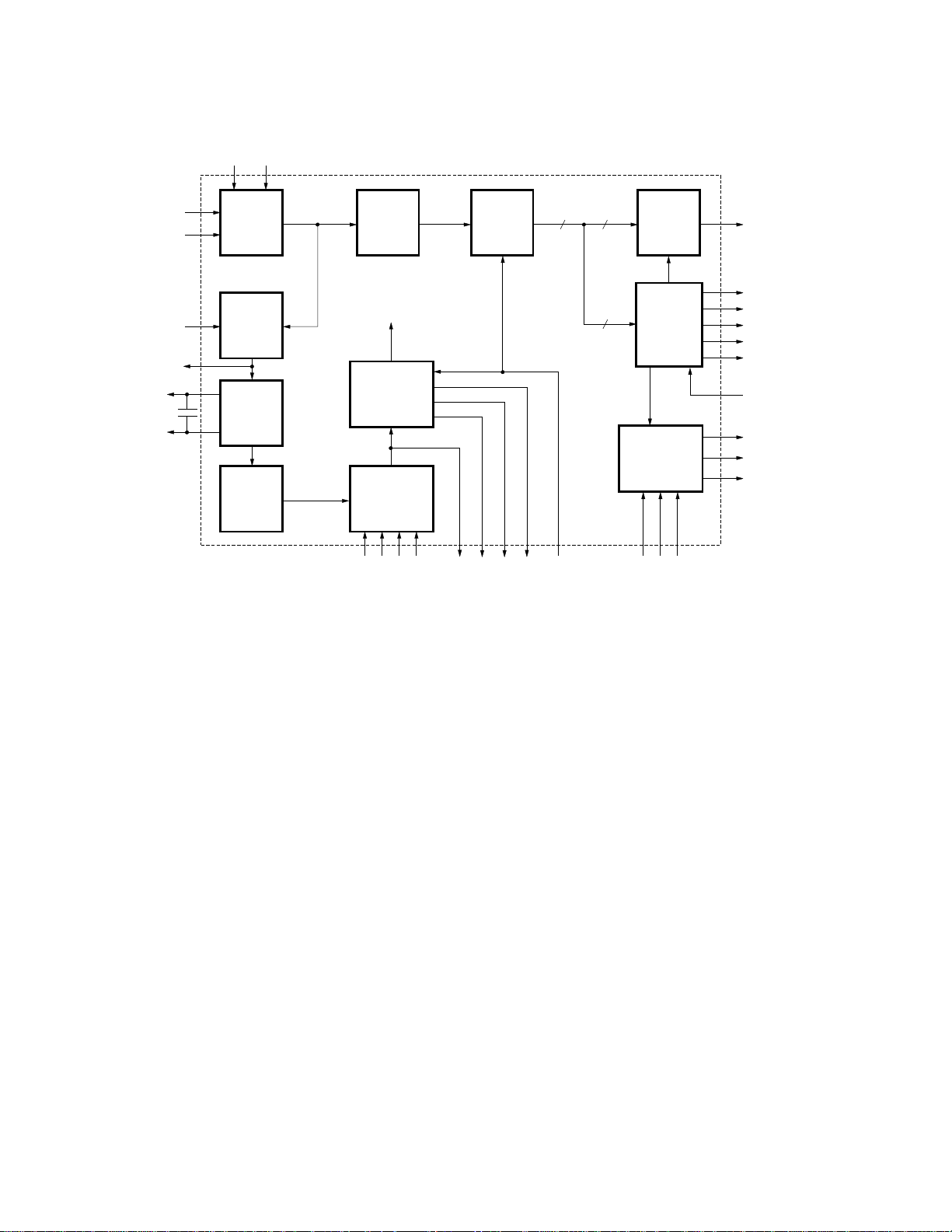
Figure 5. HDMP-1014 Receiver Block Diagram.
INPUT
SELECT
PHASE /
FREQ
DETECT
FILTER
VCO
SAMPLER
INTERNAL
GENERATOR
TCLK
INPUT
CLOCKS
CLOCK
CLOCK
SELECT
TCLKSEL
DIV1
DIV0
BCLK
FRAME
DEMUX
FCLK
NCLK
STRBOUT
M20SEL
D-FIELD
DECODER
C-FIELD
DECODER
STATE
MACHINE
SMRTST1*
SMRTST0*
D0..D19
FLAG
DAV*
CAV*
FF
ERROR
FLAGSEL
LINKRDY*
STAT1
STAT0
ACTIVE
HDMP-1014 Rx Block
Diagram
The HDMP-1014 receiver was
designed to convert a serial data
signal sent from the HDMP-1012
into either 16,17, 20 or 21 bit
wide parallel data. In doing this,
it performs the functions of
• Clock Recovery
• Data Recovery
• Demultiplexing
• Frame Decoding
• Frame Synchronization
• Frame Error Detection
• Link State Control
Input Select
The input select block determines
which input line is used. In
normal operation (LOOPEN=0),
DIN is accepted as the input
signal. For improved distance
and BER using coax cable, an
input equalizer may be used by
asserting EQEN. By setting
LOOPEN high, the receiver
accepts LIN as the input signal.
This feature allows for loop back
testing exclusive of the
transmission medium.
Phase/Freq Detect
This block compares either the
phase or the frequency of the
incoming signal to the internal
serial clock, generated from the
Clock Select block. The
frequency detect disable pin
(FDIS) is set high to disable the
frequency detector and enable the
phase detector. See HDMP-1014
(Rx) Phase Locked Loop for
more details. The output of this
block, PH1, is used by the filter to
determine the control signal for
the VCO.
Filter
This is a loop filter that accepts
the PH1 output from the Phase/
Freq Detector and converts it into
a control signal for the VCO. This
control signal tells the VCO
whether to increase or decrease
its frequency. The Filter uses the
PH1 input to determine a
proportional signal and an
integral signal. The proportional
signal determines whether the
VCO should increase or decrease
its frequency. The integral signal
filters out the high frequency PH1
signal and stores a historical PH1
output level. The two signals
combined determine the
magnitude of frequency change of
the VCO.
VCO
This is the Voltage Controlled
Oscillator that is controlled by the
output of the Filter. It outputs a
high speed digital signal to the
Clock Select.
580

Clock Select
The Clock Select accepts the
high speed digital signal from
the VCO and outputs an
internal high speed serial clock.
The VCO frequency is divided,
based on the DIV1/DIV0 inputs,
to the input signal’s frequency
range. The Clock Select output,
accessible through BCLK, is an
internal serial clock. It is phase
and frequency locked to the
incoming signal. This internal
serial clock is used by the Input
Sampler to sample the data. It
is also used by the Clock
Generator to generate the
recovered frame rate clock.
By setting TCLKSEL high, the
user may input an external high
speed serial clock at TCLK. The
Clock Select accepts this signal
and directly outputs it as the
internal serial clock.
Clock Generator
The Clock Generator accepts the
serial clock generated from the
Clock Select and generates the
frame rate clock, based on the
setting of M20SEL. If M20SEL
is asserted, the incoming
encoded data frame is expected
to be 24 bits wide (20 data bits
and 4 control bits). The master
transition in the control section
of encoded data stream is
expected every 24 bits, and used
to ensure proper frame synchronization of the output frame
clock, STRBOUT.
Input Sampler
The serial input signal is
converted into a serial bit
stream, using the extracted
internal serial clock from the
Clock Select. This output is
sent to the frame demux.
Frame Demux
The Frame Demux demulti-
plexes the serial bit stream from
the Input Sampler into a 20 or
24 bit wide parallel data word,
based on the setting of M20SEL.
The most significant 4 bits are
sent to the C-Field Decoder,
while the remaining 16 or 20
bits are sent to the D-Field
Decoder.
C-Field Decoder
The C-Field Decoder accepts the
control information from the
Frame Demux and determines
what kind of frame is being
received and whether or not it
has to be inverted. The control
bits are sent to the State
Machine for error checking.
The decoded information is sent
to the D-Field Decoder. CAV* is
set low if the incoming frame is
control data. DAV* is set low if
the information is data. If
neither DAV* nor CAV* is set
low, then the incoming frame is
expected to be a fill frame. If
FLAGSEL is asserted, the
FLAG bit is restored to its
original form. Otherwise, FLAG
is used to differentiate between
the even and odd frames in
Double Frame Mode. For more
information about this, refer to
Double Frame Mode.
D-Field Decoder
The D-Field Decoder accepts the
data field of the incoming data
frame from the Frame Demux.
Based on information from the
C-Field Decoder, which determines what type of data is being
received, the D-Field Decoder
restores the parallel data back
to its original form.
State Machine
The State Machine is used in
full duplex mode to perform the
functions of link startup, link
maintenance, and error checking. By setting the SMRST0*
and SMRST1* low, the user,
too, can reset the state machine
and initiate link startup.
SMRST1* is usually connected
to the transmitters LOCKED
output. STAT1 and STAT0
denote the current state of link
during startup. ACTIVE is an
input normally driven by the
STAT1 and STAT0 outputs.
This ACTIVE input is retimed
by STRBOUT and presented to
the user as LINKRDY*.
LINKRDY* is an active low
output that indicates when the
link is ready to transmit data.
Refer to The State Machine
Handshake Protocol section on
page 600 for more details.
581
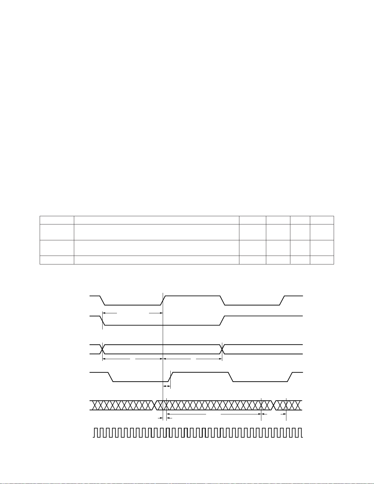
HDMP-1012 (Tx) Timing
Figure 6 shows the Tx timing
diagram. Under normal
operations, the Tx PLL locks an
internally generated clock to the
incoming STRBIN. The incoming
data, D0-D19, ED, FF, DAV*,
CAV*, and FLAG, are latched by
this internal clock. For
MDFSEL=0, the input rate of
STRBIN is expected to be the
same as the parallel data rate. For
MDFSEL=1, STRBIN should be 1/
2 of the incoming parallel data
rate. The data must be valid
before it’s sampled for the set-up
time (ts), and remain valid after
it’s sampled for the hold time (th).
The set-up and hold times are
referenced to STRBIN. This
reference is the positive edge of
STRBIN for MDFSEL=0, and is 1/
2 the frame period from the
positive or negative edge of
STRBIN for MDFSEL=1.
STRBOUT appears after this
reference with a delay of T
strb
.
the same as the word rate of the
incoming data, independent of
MDFSEL.
The start of a frame, D0, in the
high speed serial output occurs
after a delay of td after the rising
edge of the STRBIN. The typical
value of td may be calculated by
using the following formula:
td = ( 2 * serial bit duration -
0.5 ns) ns
The rate of STRBOUT is always
HDMP-1012 (Tx) Timing Characteristics
Tc = 0°C to +85°C, VEE = -4.5 V to -5.5 V
Symbol Parameter Units Min. Typ. Max.
∆T
t
t
s
h
strb
Setup Time, for Rising Edge of STRBIN Relative to nsec 6
D0-D19, ED, FF, DAV*, CAV* and FLAG
Hold Time, for Rising Edge of STRBIN Relative to nsec 0
D0-D19, ED, FF, DAV*, CAV* and FLAG
STRBOUT - STRBIN Delay nsec 1.5 3
STRBIN
MDFSEL = 0
1/2 FRAME PERIOD
STRBIN
MDFSEL = 1
D00 - D19
ED, FF
DAV*, CAV*
FLAG
STRBOUT
DOUT
HCLK
Figure 6. HDMP-1012 (Tx) Timing Diagram.
t
s
582
t
h
t
strb
D-FIELD C-FIELD
t
d
HDMP-1014 (Rx) Timing
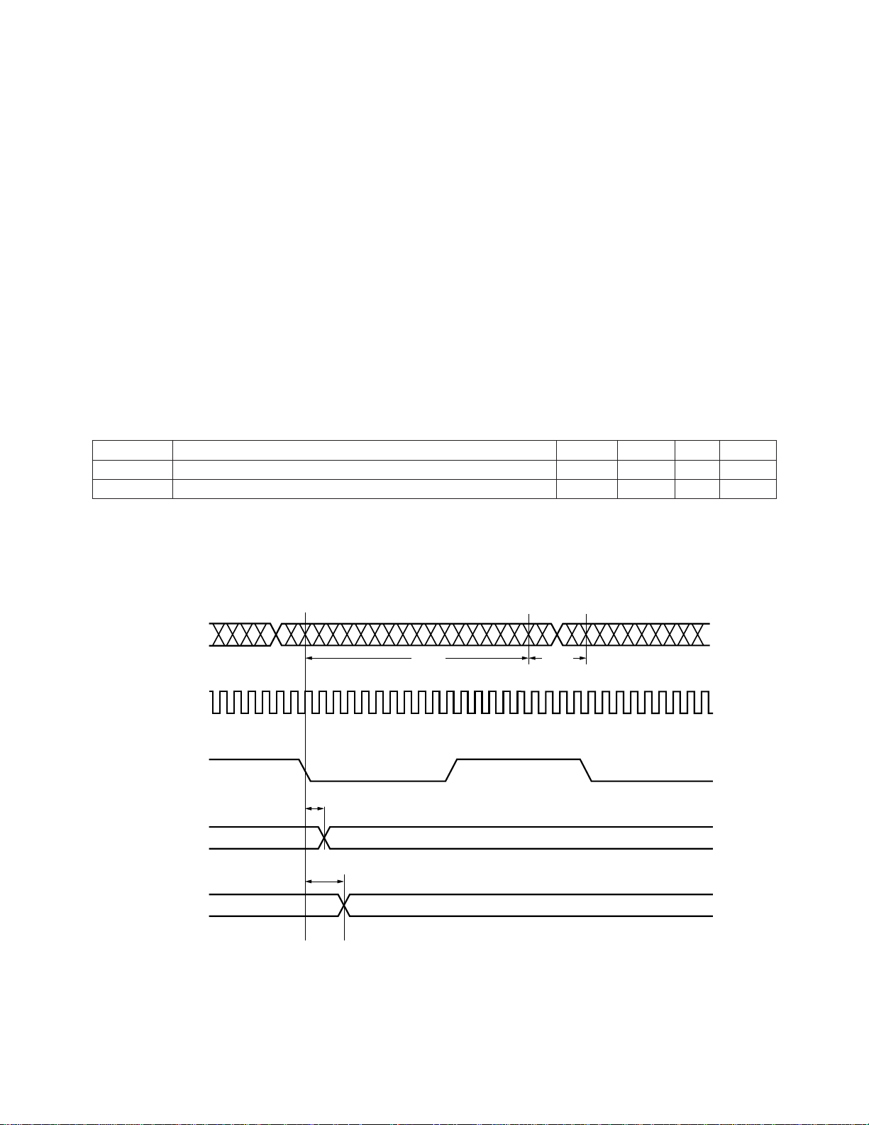
Figure 7 is the Rx timing diagram
when the internal PLL is locked to
to the data frame’s boundary,
while the rising edge is in the
center of the data frame.
the input of the serial data frame
to the update of the synchronous
outputs.
the incoming serial data. The
BCLK’s frequency is the same as
the input data rate. The size of
the input data frame can be either
20 bits or 24 bits, depending on
the setting of M20SEL.
Independent of the frame size,
STBROUT’s falling edge is aligned
The synchronous outputs, D00-
D19, LINKRDY*, DAV*, CAV*,
FF, ERROR, and FLAG, are
updated for every data frame,
with a delay of td1 after the falling
edge of STRBOUT. There is a
latency delay of two frames from
The state machine outputs,
STAT0, and STAT1, appear with
the falling edge of STRBOUT after
a delay of td2. These outputs are
updated once every 128 frames.
HDMP-1014 (Rx) Timing Characteristics
Tc = 0°C to +85°C
Symbol Parameter Units Min. Typ. Max.
t
d1
t
d2
Synchronous Output Delay nsec 2.0
State Machine Output Delay nsec 4.0
DIN
BCLK
STRBOUT
t
d1
D00 - D19
LINKRDY*
DAV*, CAV*
FF, ERROR
FLAG
t
d2
STAT1
STAT0
Figure 7. HDMP-1014 (Rx) Timing Diagram.
D-FIELD C-FIELD
583
HDMP-1012 (Tx), HDMP-1014 (Rx)
DC Electrical Specifications
Tc = 0°C to +85°C, GND = Ground, VEE = -4.5 V to -5.5 V
Symbol Parameter Units Min. Typ. Max.
V
IH,ECL
V
IL,ECL
V
OH,ECL
V
OL,ECL
V
IP,H50
V
DC,BLL
V
OP,BLL
I
EE,Tx
I
EE,Rx
Note:
1. BLL outputs are measured with external 150 Ω pull-up resistors to ground. Refer to Figure 23 for additional information.
ECL Input High Voltage Level, Guaranteed high signal mV -1150
for all inputs
ECL Input Low Voltage Level, Guaranteed low signal mV -1500
for all inputs
ECL Output High Voltage Level, Terminated with mV -1050
300 Ω to -2.0 V
ECL Output Low Voltage Level, Terminated with mV -1600
300 Ω to -2.0 V
H50 Input Peak-To-Peak Voltage mV 200
BLL Output Bias Voltage Level mV -900
BLL Output Peak-To-Peak Voltage, Terminated mV +600
with 50 Ω, ac coupled
Transmitter VEE Supply Current, with HCLKSEL off mA +403
Tc = 50°C
Receiver VEE Supply Current, Tc = 50°C mA +512
HDMP-1012 (Tx), HDMP-1014 (Rx)
AC Electrical Specifications
Tc = 25°C
Symbol Parameter Units Min. Typ. Max.
tr,ECL ECL Rise Time, Terminated with 300 Ω to -2.0 V nsec 1
tf,ECL ECL Fall Time, Terminated with 300 Ω to -2.0 V nsec 4.5
tr, BLL BLL Rise Time, Terminated with 50 Ω, ac coupled psec 200
tf,BLL BLL Fall Time, Terminated with 50 Ω, ac coupled psec 170
VSWR
i,H50
VSWR
o,BLL
Note:
1. BLL outputs are measured with external 150 Ω pull-up resistors to ground. Refer to Figure 23 for additional information.
H50 Input VSWR 2:1
BLL Output VSWR 2:1
HDMP-1012 (Tx), HDMP-1014 (Rx)
Typical Lock-Up Time
Tc = 25°C
DIV1 DIV0 HDMP-1012, msec HDMP-1014, msec LINK
0 0 2.0 2.2 2.5
0 1 3.0 3.2 3.5
1 0 4.5 4.7 5.0
1 1 8.0 11.0 12.0
Note:
1. Measured in Local Loop-Back mode with the state machine engaged and 0 cable length.
[1]
, msec
584
HDMP-1012 (Tx), HDMP-1014 (Rx)
Absolute Maximum Ratings
Tc = 25°C, except as specified. Operation in excess of any one of these conditions may result in permanent
damage to this device.
Symbol Parameter Units Min. Max.
V
V
IN,ECL
V
IN,BLL
I
O,ECL
T
T
T
EE
stg
J
max
Supply Voltage V -7 +0.5
ECL Input Voltage V -3 +0.5
H50 Input Voltage V -2 +1
ECL Output Source Current mA +50
Storage Temperature °C -40 +130
Junction Temperature °C -40 +130
Maximum Assembly Temperature (for 10 seconds maximum) °C +260
HDMP-1012 (Tx)
Thermal Characteristics, TA = 25°C
Symbol Parameter Units Typ.
Θ
jc
P
D
Thermal Resistance Die to Case °C/Watt 12
Power Dissipation, V
= -5 volts Watt 2.0
EE
HDMP-1014 (Rx)
Thermal Characteristics, TA = 25°C
Symbol Parameter Units Typ.
Θ
jc
P
D
Thermal Resistance Die to Case °C/Watt 12
Power Dissipation, VEE = -5 volts Watt 2.6
I/O Type Definitions
I/O Type Definition
I-ECL Input ECL. Similar to 100 K ECL, but with pull-down. Thus if the input is left
unconnected, the buffer generates a default value of “0”. The input can also be directly
connected to ground to generate a “1”.
O-ECL Output ECL. Similar to 100 K ECL but should be terminated with RTT ≥ 300 Ω, and do
not exceed 10cm connection distance.
O-BLL 50 matched output driver. Will drive AC coupled 50 Ω loads, with 150 Ω pull-up
resistors for broad band matching. All unused outputs should have 150 Ω pull-up
resistors, and AC coupled to a 50 Ω resistor to ground.
I-H50 Input with internal 50 Ω terminations. Input is diode level shifted so that it can swing
around ground. Can be driven with single-end configuration. Commonly used with input
single-end AC coupling from an O-BLL driver or another 50 Ω source, or differential
direct coupling from an O-BLL driver.
C Filter capacitor node.
S Power supply or ground.
585
 Loading...