


Low Cost Gigabit Rate
Transmit/Receive Chip Set
Technical Data
HDMP-1012 Transmitter
HDMP-1014 Receiver
Features
• Transparent, Extended
Ribbon Cable Replacement
• Implemented in a Low Cost
Aluminum M-Quad 80
Package
• High-Speed Serial Rate 150-
1500 MBaud
• Standard 100K ECL
Interface
16, 17, 20, or 21 Bits Wide
• Reliable Monolithic Silicon
Bipolar Implementation
• On-chip Phase-Locked Loops
- Transmit Clock Generation
- Receive Clock Extraction
Applications
• Backplane/Bus Extender
• Video, Image Acquisition
• Point to Point Data Links
• Implement SCI-FI Standard
• Implement Serial HIPPI
Specification
Description
The HDMP-1012 transmitter and
the HDMP-1014 receiver are used
to build a high speed data link for
point to point communication.
The monolithic silicon bipolar
transmitter chip and receiver chip
are each provided in a standard
aluminum M-Quad 80 package.
From the user’s viewpoint, these
products can be thought of as
providing a “virtual ribbon cable”
interface for the transmission of
data. Parallel data loaded into the
Tx (transmitter) chip is delivered
to the Rx (receiver) chip over a
serial channel, which can be
either a coaxial copper cable or
optical link.
The chip set hides from the user
all the complexity of encoding,
multiplexing, clock extraction,
demultiplexing and decoding.
Unlike other links, the phaselocked-loop clock extraction
circuit also transparently provides
for frame synchronization - the
user is not troubled with the
periodic insertion of frame
synchronization words. In
addition, the dc balance of the
line code is automatically
maintained by the chip set. Thus,
the user can transmit arbitrary
data without restriction. The Rx
chip also includes a state-machine
controller (SMC) that provides a
startup handshake protocol for
the duplex link configuration.
The serial data rate of the T/R link
is selectable in four ranges (see
tables on page 5), and extends
from 120 Mbits/s up to 1.25
Gbits/s. The parallel data interface
is 16 or 20 bit single-ended ECL,
pin selectable. A flag bit is
available and can be used as an
extra 17th or 21st bit under the
user’s control. The flag bit can
also be used as an even or odd
frame indicator for dual-frame
transmission. If not used, the link
performs expanded error
detection.
The serial link is synchronous,
and both frame synchronization
5962-0049E (6/94)
573

and bit synchronization are
maintained. When data is not
available to send, the link
maintains synchronization by
transmitting fill frames. Two
(training) fill frames are reserved
for handshaking during link
startup.
User control space is also supported. If Control Available is
asserted at the Tx chip, the least
significant 14 or 18 bits of the
data are sent and the Rx Control
Available line will indicate the
data as a Control Word.
It is the intention of this data
sheet to provide the design
engineer all of the information
regarding the HDMP-1012/1014
chipset necessary to design this
product into their application. To
assist you in using this data sheet,
the following Table of Contents is
provided.
Table of Contents
Topic Page
Typical Applications ....................................................................... 575
Setting the Operating Rate ..............................................................576
Transmitter Block Diagram .............................................................578
Receiver Block Diagram ................................................................. 580
Transmitter Timing Characteristics ................................................ 582
Receiver Timing Characteristics ..................................................... 583
DC Electrical Specifications ........................................................... 584
AC Electrical Specifications ............................................................584
Typical Lock-Up Times ................................................................... 584
Absolute Maximum Ratings ............................................................ 585
Thermal Characteristics ................................................................. 585
I/O Type Definitions ....................................................................... 585
Pin-Out Diagrams .......................................................................... 586
Transmitter Pin Definitions ............................................................ 587
Receiver Pin Definitions ................................................................. 591
Mechanical Dimensions and
Surface Mount Assembly Instructions ......................................... 595
Appendix I: Additional Internal
Architecture Information ........................................................596
Line Code Description .................................................................... 596
Data Frame Codes ......................................................................... 596
Control Frame Codes ..................................................................... 597
Fill Frame Codes ............................................................................ 598
Tx Operation Principles ................................................................. 599
Tx Encoding .................................................................................. 599
Tx Phase Locked Loop ....................................................................600
Rx Operation Principles ................................................................. 601
Rx Encoding ...................................................................................601
HDMP-1014 (Rx) Phase Locked Loop ............................................ 601
HDMP-1014 (Rx) Decoding ............................................................602
HDMP-1014 (Rx) Link Control State
Machine Operation Principle .......................................................603
The State Machine Handshake Protocol ..........................................603
Appendix II: Link Configuration Examples .............................605
Duplex/Simplex Configurations ...................................................... 605
Full Duplex .....................................................................................605
Simplex Method I: Simplex with Low Speed Return Path ...............606
Simplex Method II: Simplex with Periodic Sync Pulse ....................607
Simplex Method III: Simplex with
External Reference Oscillator ......................................................607
Data Interface for Single/Double Frame Mode ................................ 608
Single Frame Mode (MDFSEL=0) .................................................. 608
Double Frame Mode (MDFSEL=1) ................................................ 609
Supply Bypassing and Integrator Capacitor .................................... 610
Integrating Capacitor ......................................................................610
Power Supply Bypassing and Grounding ........................................ 610
Electrical Connections ....................................................................611
I-ECL and O-ECL ............................................................................611
High Speed Interface: I-H50 & O-BLL ............................................612
TTL and Positive 5 V Operation ......................................................613
Mode Options ................................................................................. 614
574
Typical Applications
The HDMP-1012/1014 chipset
was designed for ease of use and
flexibility. This allows the
customer to tailor the use of this
product, through the configuration of the link, based on their
specific system requirements and
application needs. Typical
applications range from
backplane and bus extension to
digital video transmission.
Low latency bus extension of a 16
or 20 bit wide data bus may be
achieved using the standard
duplex configuration (see Figure
1d). In full duplex, the HDMP1012/1014 chipset handles all of
the issues of link startup, maintenance, and simple error
detection.
If the bus width is 32 or 40 bits
wide, the HDMP-1012/1014
chipset is capable of sending the
large data frame as two separate
frame segments, as shown in
Figure 1b. In this mode, called
Double Frame Mode, the FLAG
bit is used by the transmitter and
receiver to indicate the first or
second frame segment. The
HDMP-1012/1014 chipset in
Double Frame Mode may also be
configured in full duplex to
achieve a 32/40 bit wide bus
extension.
For digital video transmission,
simplex links are more common.
The HDMP-1012/1014 chipset
can transmit 16 to 21 bits of
parallel data in standard or
broadcast simplex mode.
Additionally, 32 to 40 bit wide
data can be transmitted over a
single line (in Double Frame
Mode) or two parallel lines, as in
Figure 1c.
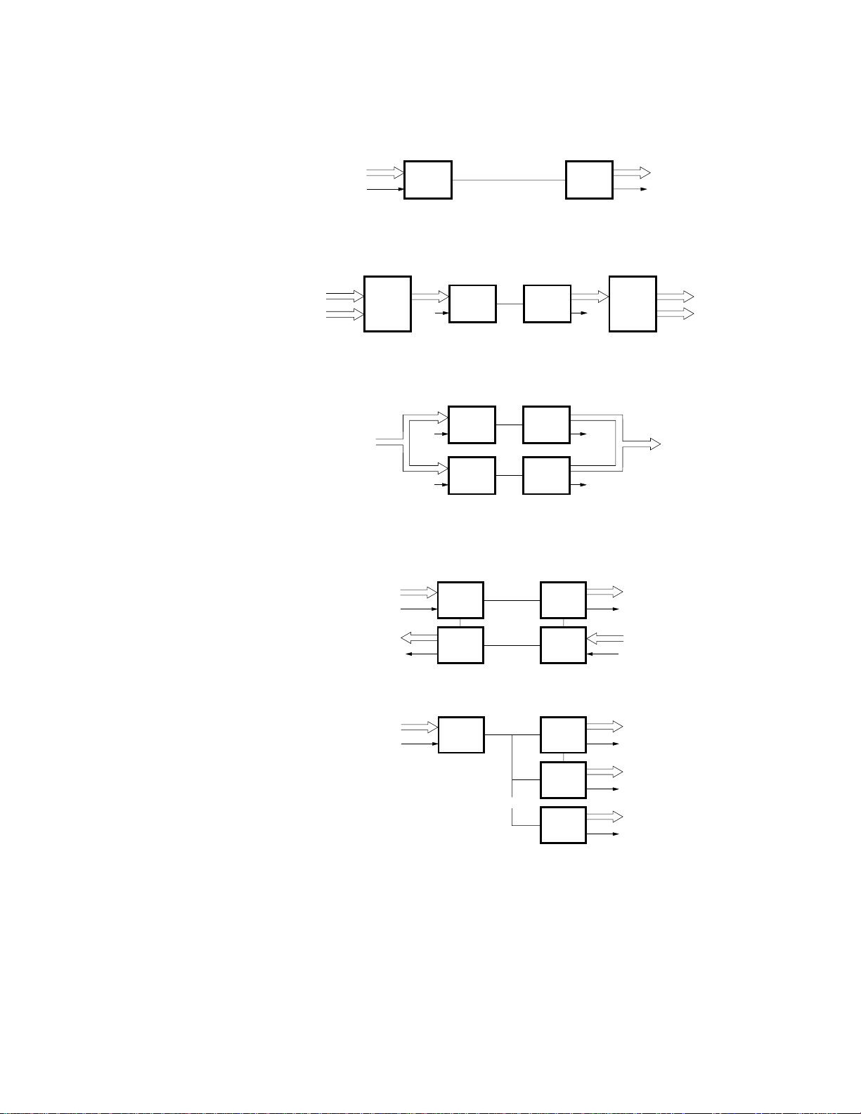
CLK CLK
MUX
Tx Rx
A) 16/20 BIT SIMPLEX TRANSMISSION
CLK
CLK
CLK
CLK
CLK
CLK
Tx Rx
B) 32/40 BIT SIMPLEX TRANSMISSION
Tx Rx
Tx Rx
C) 32/40 BIT SIMPLEX TRANSMISSION
WITH HIGH CLOCK RATES
Tx Rx
Rx Tx
D) 16/20 BIT DUPLEX TRANSMISSION
Tx Rx
E) SIMPLEX BROADCAST TRANSMISSION
DEMUX
CLK
CLK
CLK
CLK
CLK
CLK
Rx
.
.
.
.
.
.
.
.
Rx
CLK
CLK
Figure 1. Various Configurations Using the HDMP-1012/1014.
575

For timing diagrams for the
standard configurations, see the
Appendix section entitled Link
Configuration Examples.
The HDMP-1012/1014 chipset can support serial transmission rates from 150 MBd to 1.5 GBd for each of these configurations. The chipset requires the user to input the link data rate by asserting DIV1 and DIV0 accordingly. To determine the DIV1/DIV0 setting necessary for each application, refer to the section: Setting the Operating Data Rate Range on the next page.
Setting the Operating
Data Rate Range
The HDMP-1012/1014 chipset
can operate from 150 MBaud to
1500 MBaud. It is divided into
four operating data ranges with
each range selected by setting
DIV1 and DIV0 as shown in the
tables below.
The purpose of following example
is to help in understanding and
using these tables. This specific
example uses the table in figure 3
entitled “Typical 20-bit Mode Data
Rates”.
It is desired to transmit a 20 bit
parallel word operating at 55 MHz
(55 MWord/sec). Both the Tx and
Rx must be set to a range that this
word rate falls in-between.
According to table entitled
“Typical Operating Rates for 20
Bit Mode” on the next page, a
setting of DIV1/DIV0 = logic ‘0/0’
allows a parallel input word rate
of 32.9 to 62.5 MHz . This setting
easily accommodates the required
55 MHz word rate. The user serial
data rate can be calculated as:
Serial
Data Rate = (––––––) (––––––)
The baud rate includes an
additional 4 bits that G-LINK
transmits for link control and
error detection. The serial baud
rate is calculated as:
Serial
Baud Rate = (––––––) (––––––)
The 55 MHz example is one in
which the parallel word rate
provides only one possible DIV1/
DIV0 setting.
20 bit 55 Mw
word sec
= 1100 MBits/sec
24 bits 55 Mw
word sec
= 1320 MBaud
Some applications may have a
parallel word rate that seems to fit
two ranges. As an example, a 35
MHz (35 MWord/s) parallel data
rate fall within two ranges (DIV0/
DIV1 = 0/0 and DIV0/DIV1 = 0/
1) in 20 Bit Mode. Per the table, a
setting of DIV1/DIV0 = 0/1 gives
an upper rate of 53.3 MHz , while
a setting of DIV1/DIV0 = 0/0
gives a lower rate of 32.9 MHz.
These transition data rates are
stated in the tables as typical
values and may vary between
individual parts. Each transmitter/
receiver has continuous band
cover across its entire 150 to
1500 MBaud range and has
overlap between ranges. Each
transmitter/receiver will permit a
35 MHz parallel data rate, but it is
suggested that DIV0 be a jumper
that can be set either to logic ‘1’
(ground) or logic ‘0’ (open). This
allows the design to accommodate
both ranges for maximum
flexibility. This technique is
recommended whenever
operating near the maximum and
minimum of two word rate
ranges. The above information
also applies to the HDMP-1012/
1014 chipset when operating in
16 bit mode.
576
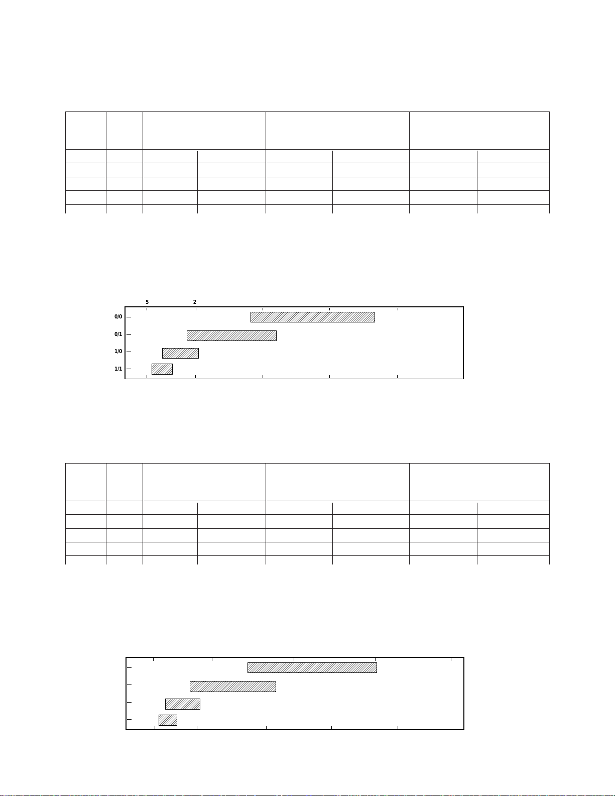
HDMP-1012 (Tx), HDMP-1014 (Rx)
Typical Operating Rates For 16 Bit Mode
Tc = 0°C to +85°C, VEE = -4.5 V to -5.5 V
Parallel Word Rate Serial Data Rate Serial Baud Rate
(Mword/sec) (Mbit/sec) (MBaud)
DIV1 DIV0 Range Range Range
0 0 42 75.0 (max) 672 1200.0 (max) 840 1500.0 (max)
0 1 21 51 336 808 420 1010
1 0 11 25 168 404 210 505
1 1 7.5 (min) 13 120.0 (min) 202 150.0 (min) 253
Notes:
1. Extended operating rates to 1800 MBaud/sec (typ) are possible for Tc = 0°C to +60°C.
2. All values are typical over temperature and process, unless otherwise noted by (min) or (max).
3. Typical Serial Baud Rates for DIV1/DIV0 = 0/0 are up to 1800 MBd.
4. All values in this table are expected for a BER less than 10
which was performed at a serial data rate of 2000 Mbits/s for a BER less than 10
BER = 10-7.
[1]
-14
. This estimation is based on the maximum data rate characterization,
-11
. Production units are 100% screened for less than
FRAME RATE (Mwords/sec)
840
1010
SERIAL DATA RATE (Mbaud)
1800
BAUD RATE = 20 x FRAME RATE
2500200015001000500100
0/0
0/1
1/0
DIV 1 / DIV 0
1/1
5 25 50 75 100 125
420
210
110 253
505
Figure 2: Typical 16-bit Mode Data Rates.
HDMP-1012 (Tx), HDMP-1014 (Rx)
Typical Operating Rates For 20 Bit Mode
Tc = 0°C to +85°C, VEE = -4.5 V to -5.5 V
Parallel Word Rate Serial Data Rate Serial Baud Rate
(Mword/sec) (Mbit/sec) (MBaud/Sec)
DIV1 DIV0 Range Range Range
0 0 35 62.5 (max) 700 1250.0 (max) 840 1500 (max)
0 1 18 42 350 842 420 1010
1 0 9 21 175 421 210 505
1 1 6.3 (min) 10.5 125.0 (min) 211 150 (min) 253
Notes:
1. Extended operating rates to 1800 MBaud/sec are possible for Tc = 0°C to +60°C.
2. All values are typical over temperature and process, unless otherwise noted by (min) or (max).
3. Typical Serial Baud Rates for DIV1/DIV0 = 0/0 are up to 1800 MBd.
4. All values in this table are expected for a BER less than 10
which was performed at a serial data rate of 2000 Mbits/s for a BER less than 10
BER = 10-7.
[1]
-14
. This estimation is based on the maximum data rate characterization,
-11
. Production units are 100% screened for less than
4 25 50 75 100
0/0
0/1
1/0
DIV 1 / DIV 0
1/1
110 253
210
420
505
Figure 3. Typical 20-Bit Mode Data Rates.
FRAME RATE (Mwords/sec)
840
1010
SERIAL DATA RATE (Mbaud)
1800
BAUD RATE = 24 x FRAME RATE
2500200015001000500100
577
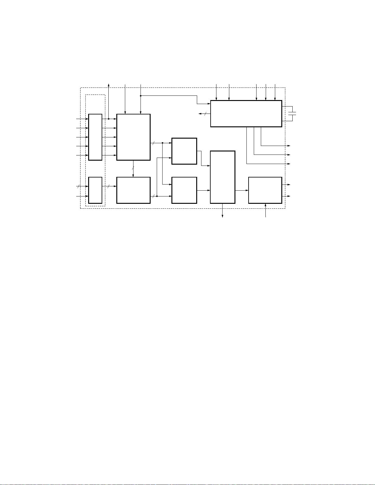
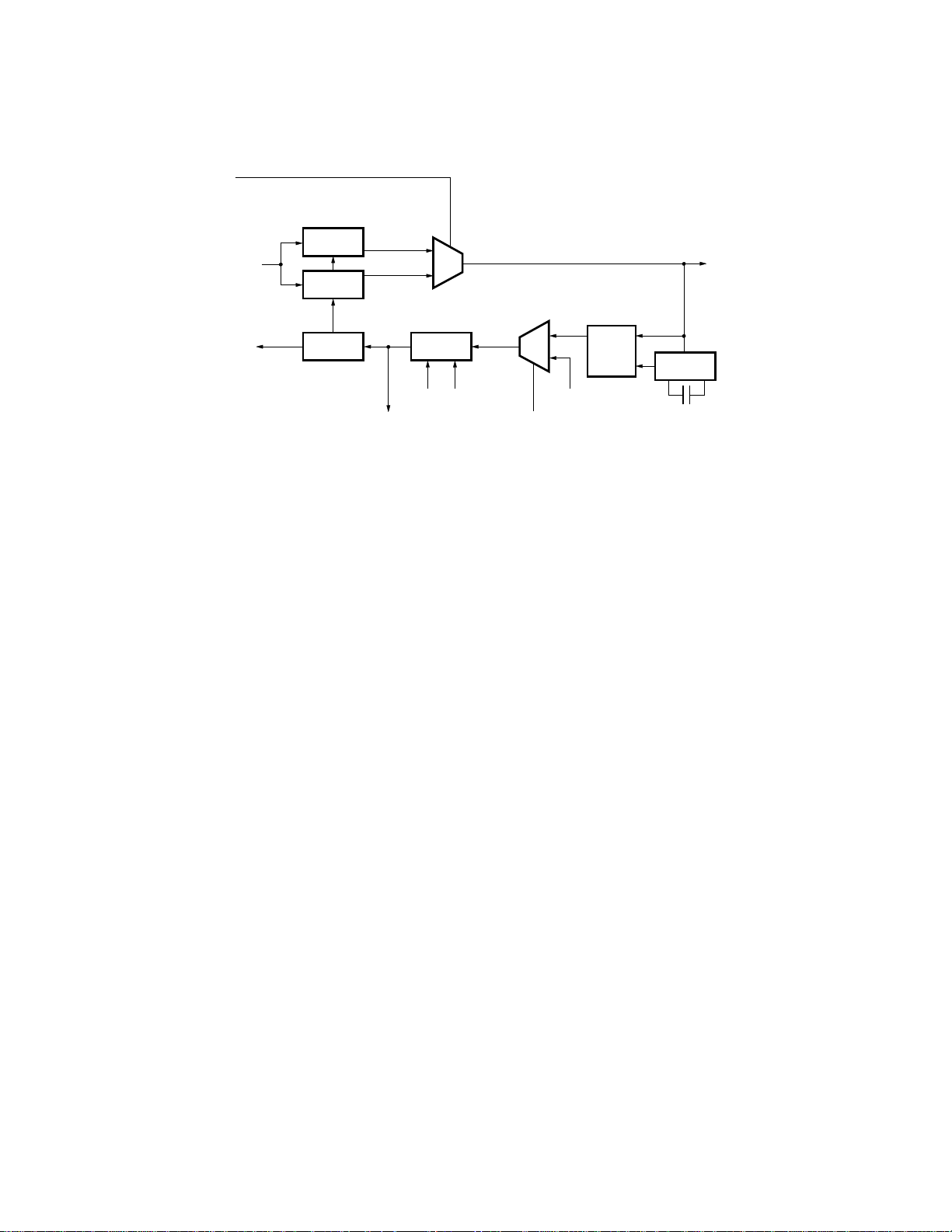
RFD
FLAGSEL
M20SEL
STRBIN
EHCLKSEL
DIV0
DIV1
MDFSEL
INPUT
LATCH
ED
FF
CAV*
DAV*
FLAG
D0-D19
RST*
Figure 4. HDMP-1012 Transmitter Block Diagram.
LATCHLATCH
HDMP-1012 Tx Block Diagram
The HDMP-1012 was designed to
accept 16 or 20 bit wide parallel
data and transmit it over a high
speed serial line, while minimizing
the user’s necessary interface to
the high speed circuitry. In order
to accomplish this task, the
HDMP-1012 performs the
following functions:
• Parallel Word Input
• High Speed Clock Multiplication
• Frame Encoding
• Parallel to Serial Multiplexing
CONTROL
LOGIC
+
C-FIELD
ENCODER
D-FIELD
ENCODER
incoming frame clock. The PLL/
Clock Generator locks on to this
incoming rate and multiplies the
clock up to the needed high speed
serial clock. Based on M20SEL,
which determines whether the
incoming data frame is 16 or 20
bits wide, the PLL/Clock
Generator multiplies the frame
rate clock by 20 or 24
respectively (data bits + 4 control
bits). DIV1/DIV0 are set to inform
the transmitter of the frequency
range of the incoming data
frames. The internal frame rate
clock is accessible through
STRBOUT and the high speed
PLL/Clock Generator
The Phase Lock-loop and Clock
serial clock is accessible through
HCLK.
Generator are responsible for
generating all internal clocks
needed by the transmitter to
perform its functions. These
clocks are based on a supplied
frame clock (STRBIN) and control
signals (M20SEL, MDFSEL,
EHCLKSEL, DIV1, DIV0). In
normal operation (MDFSEL=0),
When MDFSEL is set high, the
transmitter is in Double Frame
Mode. Using this option, the user
may send a 32 or 40 bit wide data
frame in two segments while
supplying the original 32 or 40 bit
frame clock at STRBIN. Doubling
of the frame rate is performed by
STRBIN is expected to be the
INTERNAL
CLOCKS
SIGN
FRAME
MUX
PLL / CLOCK
GENERATOR
OUTPUT
ACCUMULATE / INVERT
SELECT
LOOPENINV
the transmitter. The clock
generator section performs the
clock multiplication to the
necessary serial clock rate.
By setting EHCLKSEL high, the
user may provide an external high
speed serial clock at STRBIN.
This clock is used directly by the
high speed serial circuitry to
output the serial data.
Control Logic and C-Field Encoder
The Control Logic is responsible
for determining what information
is serially sent to the output. If
CAV* is low, it sends the data at
D0..D8 and D9..D17 as control
word information. If CAV* is high
and DAV* is low, it sends parallel
word data at the data inputs. If
neither CAV* nor DAV* is set low,
then the transmitter assumes the
link is not being used. In this
state, the control logic triggers
the Data Encoder to send Fill
Frames to maintain the link DC
balance and allow the receiver to
CAP0
0.1 µF
CAP1
STRBOUT
HCLK
LOCKED
DOUT
LOUT
578

maintain frequency and phase
lock. The type of fill frames sent
(FF0 or FF1) is determined by the
FF input. In a duplex system, FF
is normally connected to the Rx’s
STAT1 pin.
The C-Field Encoder, based on
the inputs at DAV*, CAV*,
FLAGSEL, and FLAG, supplies
four encoded bits to the frame
mux. This encoded data contains
the master transition (which the
receiver uses for frequency
locking), as well as information
regarding the data type: control,
data, or fill frame. In order for the
FLAG bit to be used as an
additional data bit, FLAGSEL
must be set high for both the Tx
and the Rx.
D-Field Encoder
The D-Field Encoder provides the
remaining parallel word data to
the frame mux. Based on control
signals from the Control Logic,
the D-Field Encoder either
outputs the parallel information at
its data inputs (D0..D19) or the
designated Fill Frame. RST*,
when set low, resets the internal
chip registers.
Frame Mux
The Frame Mux accepts the
output from the C-Field and D-
Field Encoders. The four control
bits are attached to the data bits,
either 16 or 20 data bits based on
the M20SEL input. This parallel
information, now either 20 or 24
bits wide, is multiplexed to a
serial line based on the internal
high speed serial clock.
SIGN
The sign circuitry determines the
cumulative sign of the outgoing
data frame, containing the data
and control bits. This is used by
the accumulator/inverter to
maintain DC balance for the
transmission line.
Accumulator/Invert
The Accumulator/Invert block is
responsible for maintaining the
DC balance of the serial line. It
determines, based on history and
the sign of the current data frame,
whether or not the current frame
should be inverted to bring the
line closer to the desired 50%
duty cycle. INV is set high when
the data frame is inverted.
Output Select
In normal operation, the serial
data stream is placed at DOUT.
By asserting LOOPEN, the user
may also direct the serial data
stream to LOUT, which may be
used for loopback testing. When
LOOPEN is not asserted, LOUT is
disabled to reduce power
consumption.
579
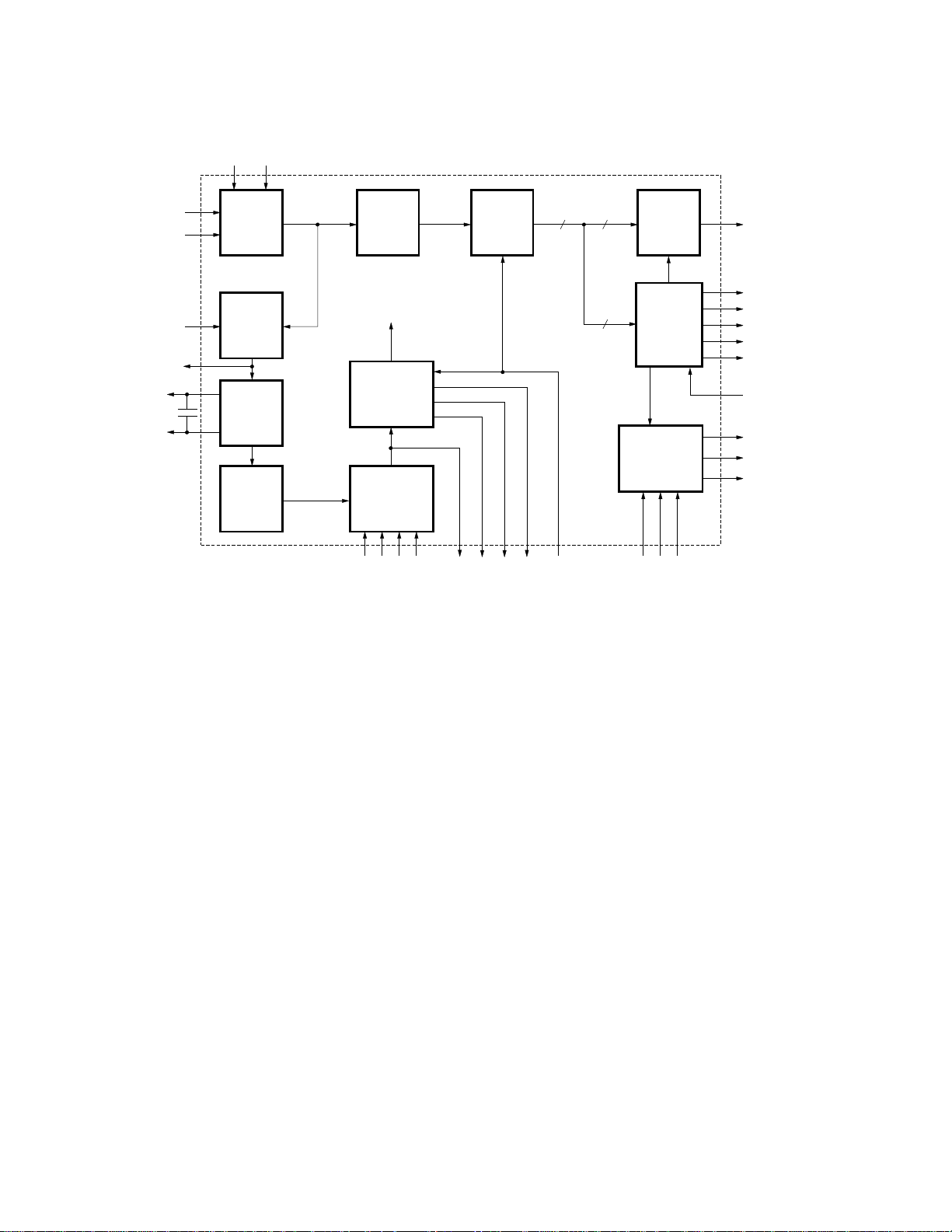
EQEN
LOOPEN
DIN
LIN
FDIS
PH1
CAP0
0.1 µF
CAP1
Figure 5. HDMP-1014 Receiver Block Diagram.
INPUT
SELECT
PHASE /
FREQ
DETECT
FILTER
VCO
SAMPLER
INTERNAL
GENERATOR
TCLK
INPUT
CLOCKS
CLOCK
CLOCK
SELECT
TCLKSEL
DIV1
DIV0
BCLK
FRAME
DEMUX
FCLK
NCLK
STRBOUT
M20SEL
D-FIELD
DECODER
C-FIELD
DECODER
STATE
MACHINE
SMRTST1*
SMRTST0*
D0..D19
FLAG
DAV*
CAV*
FF
ERROR
FLAGSEL
LINKRDY*
STAT1
STAT0
ACTIVE
HDMP-1014 Rx Block
Diagram
The HDMP-1014 receiver was
designed to convert a serial data
signal sent from the HDMP-1012
into either 16,17, 20 or 21 bit
wide parallel data. In doing this,
it performs the functions of
• Clock Recovery
• Data Recovery
• Demultiplexing
• Frame Decoding
• Frame Synchronization
• Frame Error Detection
• Link State Control
Input Select
The input select block determines
which input line is used. In
normal operation (LOOPEN=0),
DIN is accepted as the input
signal. For improved distance
and BER using coax cable, an
input equalizer may be used by
asserting EQEN. By setting
LOOPEN high, the receiver
accepts LIN as the input signal.
This feature allows for loop back
testing exclusive of the
transmission medium.
Phase/Freq Detect
This block compares either the
phase or the frequency of the
incoming signal to the internal
serial clock, generated from the
Clock Select block. The
frequency detect disable pin
(FDIS) is set high to disable the
frequency detector and enable the
phase detector. See HDMP-1014
(Rx) Phase Locked Loop for
more details. The output of this
block, PH1, is used by the filter to
determine the control signal for
the VCO.
Filter
This is a loop filter that accepts
the PH1 output from the Phase/
Freq Detector and converts it into
a control signal for the VCO. This
control signal tells the VCO
whether to increase or decrease
its frequency. The Filter uses the
PH1 input to determine a
proportional signal and an
integral signal. The proportional
signal determines whether the
VCO should increase or decrease
its frequency. The integral signal
filters out the high frequency PH1
signal and stores a historical PH1
output level. The two signals
combined determine the
magnitude of frequency change of
the VCO.
VCO
This is the Voltage Controlled
Oscillator that is controlled by the
output of the Filter. It outputs a
high speed digital signal to the
Clock Select.
580

Clock Select
The Clock Select accepts the
high speed digital signal from
the VCO and outputs an
internal high speed serial clock.
The VCO frequency is divided,
based on the DIV1/DIV0 inputs,
to the input signal’s frequency
range. The Clock Select output,
accessible through BCLK, is an
internal serial clock. It is phase
and frequency locked to the
incoming signal. This internal
serial clock is used by the Input
Sampler to sample the data. It
is also used by the Clock
Generator to generate the
recovered frame rate clock.
By setting TCLKSEL high, the
user may input an external high
speed serial clock at TCLK. The
Clock Select accepts this signal
and directly outputs it as the
internal serial clock.
Clock Generator
The Clock Generator accepts the
serial clock generated from the
Clock Select and generates the
frame rate clock, based on the
setting of M20SEL. If M20SEL
is asserted, the incoming
encoded data frame is expected
to be 24 bits wide (20 data bits
and 4 control bits). The master
transition in the control section
of encoded data stream is
expected every 24 bits, and used
to ensure proper frame synchronization of the output frame
clock, STRBOUT.
Input Sampler
The serial input signal is
converted into a serial bit
stream, using the extracted
internal serial clock from the
Clock Select. This output is
sent to the frame demux.
Frame Demux
The Frame Demux demulti-
plexes the serial bit stream from
the Input Sampler into a 20 or
24 bit wide parallel data word,
based on the setting of M20SEL.
The most significant 4 bits are
sent to the C-Field Decoder,
while the remaining 16 or 20
bits are sent to the D-Field
Decoder.
C-Field Decoder
The C-Field Decoder accepts the
control information from the
Frame Demux and determines
what kind of frame is being
received and whether or not it
has to be inverted. The control
bits are sent to the State
Machine for error checking.
The decoded information is sent
to the D-Field Decoder. CAV* is
set low if the incoming frame is
control data. DAV* is set low if
the information is data. If
neither DAV* nor CAV* is set
low, then the incoming frame is
expected to be a fill frame. If
FLAGSEL is asserted, the
FLAG bit is restored to its
original form. Otherwise, FLAG
is used to differentiate between
the even and odd frames in
Double Frame Mode. For more
information about this, refer to
Double Frame Mode.
D-Field Decoder
The D-Field Decoder accepts the
data field of the incoming data
frame from the Frame Demux.
Based on information from the
C-Field Decoder, which determines what type of data is being
received, the D-Field Decoder
restores the parallel data back
to its original form.
State Machine
The State Machine is used in
full duplex mode to perform the
functions of link startup, link
maintenance, and error checking. By setting the SMRST0*
and SMRST1* low, the user,
too, can reset the state machine
and initiate link startup.
SMRST1* is usually connected
to the transmitters LOCKED
output. STAT1 and STAT0
denote the current state of link
during startup. ACTIVE is an
input normally driven by the
STAT1 and STAT0 outputs.
This ACTIVE input is retimed
by STRBOUT and presented to
the user as LINKRDY*.
LINKRDY* is an active low
output that indicates when the
link is ready to transmit data.
Refer to The State Machine
Handshake Protocol section on
page 600 for more details.
581
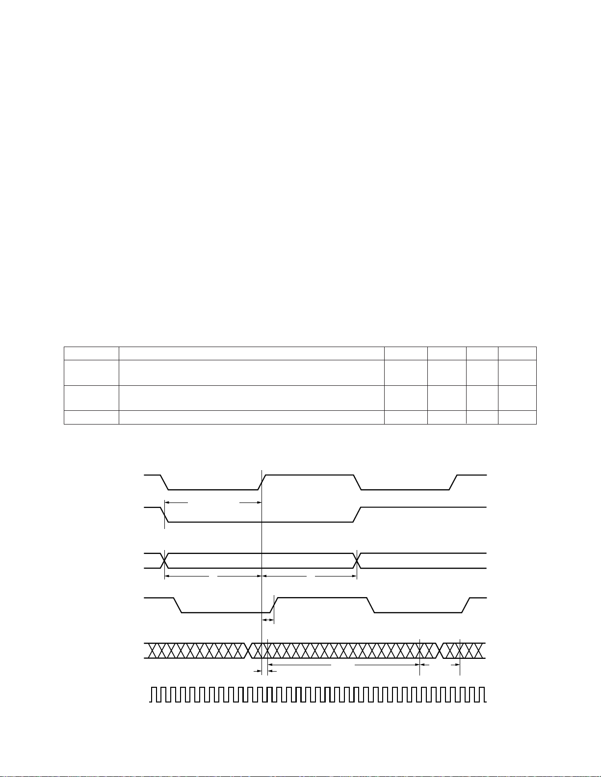
HDMP-1012 (Tx) Timing
Figure 6 shows the Tx timing
diagram. Under normal
operations, the Tx PLL locks an
internally generated clock to the
incoming STRBIN. The incoming
data, D0-D19, ED, FF, DAV*,
CAV*, and FLAG, are latched by
this internal clock. For
MDFSEL=0, the input rate of
STRBIN is expected to be the
same as the parallel data rate. For
MDFSEL=1, STRBIN should be 1/
2 of the incoming parallel data
rate. The data must be valid
before it’s sampled for the set-up
time (ts), and remain valid after
it’s sampled for the hold time (th).
The set-up and hold times are
referenced to STRBIN. This
reference is the positive edge of
STRBIN for MDFSEL=0, and is 1/
2 the frame period from the
positive or negative edge of
STRBIN for MDFSEL=1.
STRBOUT appears after this
reference with a delay of T
strb
.
the same as the word rate of the
incoming data, independent of
MDFSEL.
The start of a frame, D0, in the
high speed serial output occurs
after a delay of td after the rising
edge of the STRBIN. The typical
value of td may be calculated by
using the following formula:
td = ( 2 * serial bit duration -
0.5 ns) ns
The rate of STRBOUT is always
HDMP-1012 (Tx) Timing Characteristics
Tc = 0°C to +85°C, VEE = -4.5 V to -5.5 V
Symbol Parameter Units Min. Typ. Max.
∆T
t
t
s
h
strb
Setup Time, for Rising Edge of STRBIN Relative to nsec 6
D0-D19, ED, FF, DAV*, CAV* and FLAG
Hold Time, for Rising Edge of STRBIN Relative to nsec 0
D0-D19, ED, FF, DAV*, CAV* and FLAG
STRBOUT - STRBIN Delay nsec 1.5 3
STRBIN
MDFSEL = 0
1/2 FRAME PERIOD
STRBIN
MDFSEL = 1
D00 - D19
ED, FF
DAV*, CAV*
FLAG
STRBOUT
DOUT
HCLK
Figure 6. HDMP-1012 (Tx) Timing Diagram.
t
s
582
t
h
t
strb
D-FIELD C-FIELD
t
d
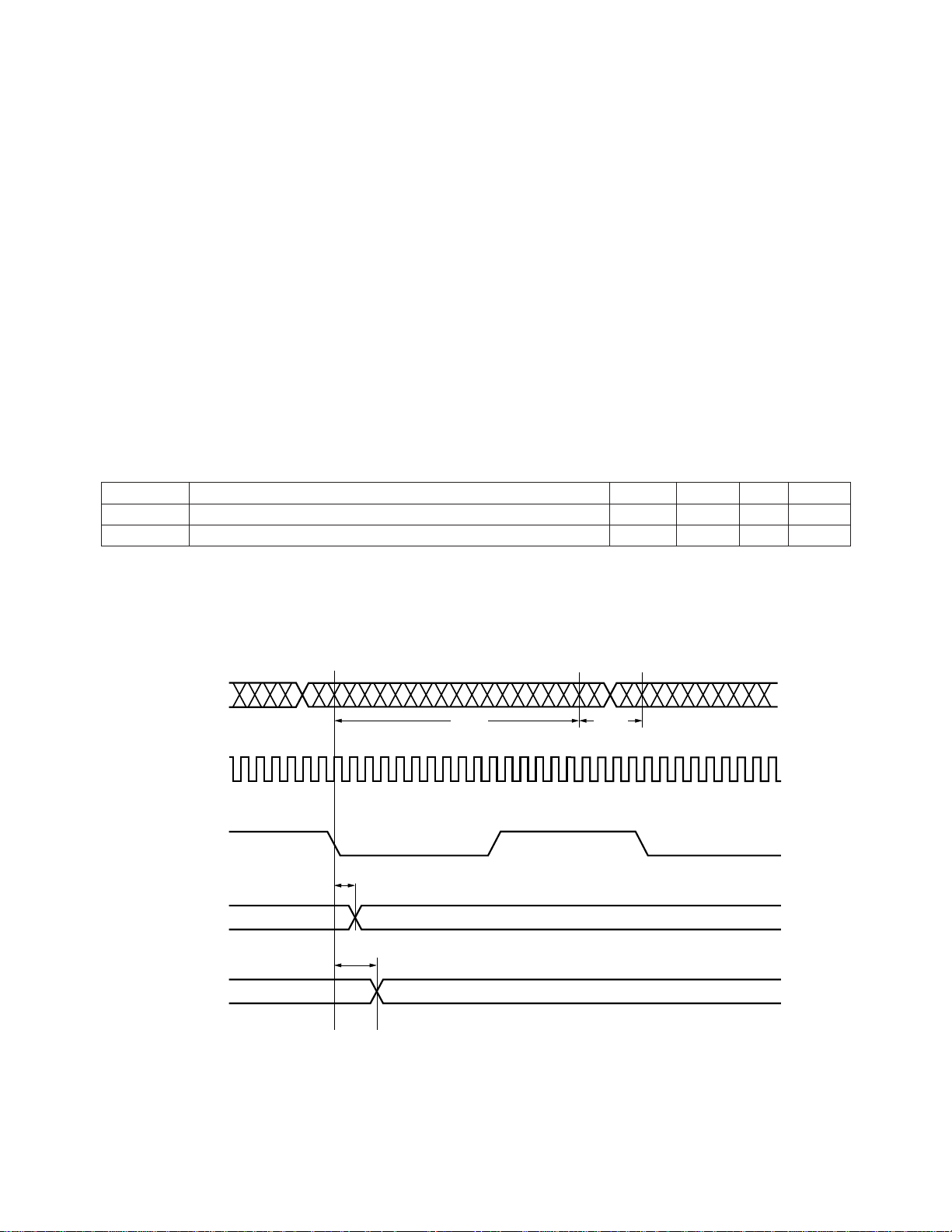
HDMP-1014 (Rx) Timing
Figure 7 is the Rx timing diagram
when the internal PLL is locked to
to the data frame’s boundary,
while the rising edge is in the
center of the data frame.
the input of the serial data frame
to the update of the synchronous
outputs.
the incoming serial data. The
BCLK’s frequency is the same as
the input data rate. The size of
the input data frame can be either
20 bits or 24 bits, depending on
the setting of M20SEL.
Independent of the frame size,
STBROUT’s falling edge is aligned
The synchronous outputs, D00-
D19, LINKRDY*, DAV*, CAV*,
FF, ERROR, and FLAG, are
updated for every data frame,
with a delay of td1 after the falling
edge of STRBOUT. There is a
latency delay of two frames from
The state machine outputs,
STAT0, and STAT1, appear with
the falling edge of STRBOUT after
a delay of td2. These outputs are
updated once every 128 frames.
HDMP-1014 (Rx) Timing Characteristics
Tc = 0°C to +85°C
Symbol Parameter Units Min. Typ. Max.
t
d1
t
d2
Synchronous Output Delay nsec 2.0
State Machine Output Delay nsec 4.0
DIN
BCLK
STRBOUT
t
d1
D00 - D19
LINKRDY*
DAV*, CAV*
FF, ERROR
FLAG
t
d2
STAT1
STAT0
Figure 7. HDMP-1014 (Rx) Timing Diagram.
D-FIELD C-FIELD
583
HDMP-1012 (Tx), HDMP-1014 (Rx)
DC Electrical Specifications
Tc = 0°C to +85°C, GND = Ground, VEE = -4.5 V to -5.5 V
Symbol Parameter Units Min. Typ. Max.
V
IH,ECL
V
IL,ECL
V
OH,ECL
V
OL,ECL
V
IP,H50
V
DC,BLL
V
OP,BLL
I
EE,Tx
I
EE,Rx
Note:
1. BLL outputs are measured with external 150 Ω pull-up resistors to ground. Refer to Figure 23 for additional information.
ECL Input High Voltage Level, Guaranteed high signal mV -1150
for all inputs
ECL Input Low Voltage Level, Guaranteed low signal mV -1500
for all inputs
ECL Output High Voltage Level, Terminated with mV -1050
300 Ω to -2.0 V
ECL Output Low Voltage Level, Terminated with mV -1600
300 Ω to -2.0 V
H50 Input Peak-To-Peak Voltage mV 200
BLL Output Bias Voltage Level mV -900
BLL Output Peak-To-Peak Voltage, Terminated mV +600
with 50 Ω, ac coupled
Transmitter VEE Supply Current, with HCLKSEL off mA +403
Tc = 50°C
Receiver VEE Supply Current, Tc = 50°C mA +512
HDMP-1012 (Tx), HDMP-1014 (Rx)
AC Electrical Specifications
Tc = 25°C
Symbol Parameter Units Min. Typ. Max.
tr,ECL ECL Rise Time, Terminated with 300 Ω to -2.0 V nsec 1
tf,ECL ECL Fall Time, Terminated with 300 Ω to -2.0 V nsec 4.5
tr, BLL BLL Rise Time, Terminated with 50 Ω, ac coupled psec 200
tf,BLL BLL Fall Time, Terminated with 50 Ω, ac coupled psec 170
VSWR
i,H50
VSWR
o,BLL
Note:
1. BLL outputs are measured with external 150 Ω pull-up resistors to ground. Refer to Figure 23 for additional information.
H50 Input VSWR 2:1
BLL Output VSWR 2:1
HDMP-1012 (Tx), HDMP-1014 (Rx)
Typical Lock-Up Time
Tc = 25°C
DIV1 DIV0 HDMP-1012, msec HDMP-1014, msec LINK
0 0 2.0 2.2 2.5
0 1 3.0 3.2 3.5
1 0 4.5 4.7 5.0
1 1 8.0 11.0 12.0
Note:
1. Measured in Local Loop-Back mode with the state machine engaged and 0 cable length.
[1]
, msec
584
HDMP-1012 (Tx), HDMP-1014 (Rx)
Absolute Maximum Ratings
Tc = 25°C, except as specified. Operation in excess of any one of these conditions may result in permanent
damage to this device.
Symbol Parameter Units Min. Max.
V
V
IN,ECL
V
IN,BLL
I
O,ECL
T
T
T
EE
stg
J
max
Supply Voltage V -7 +0.5
ECL Input Voltage V -3 +0.5
H50 Input Voltage V -2 +1
ECL Output Source Current mA +50
Storage Temperature °C -40 +130
Junction Temperature °C -40 +130
Maximum Assembly Temperature (for 10 seconds maximum) °C +260
HDMP-1012 (Tx)
Thermal Characteristics, TA = 25°C
Symbol Parameter Units Typ.
Θ
jc
P
D
Thermal Resistance Die to Case °C/Watt 12
Power Dissipation, V
= -5 volts Watt 2.0
EE
HDMP-1014 (Rx)
Thermal Characteristics, TA = 25°C
Symbol Parameter Units Typ.
Θ
jc
P
D
Thermal Resistance Die to Case °C/Watt 12
Power Dissipation, VEE = -5 volts Watt 2.6
I/O Type Definitions
I/O Type Definition
I-ECL Input ECL. Similar to 100 K ECL, but with pull-down. Thus if the input is left
unconnected, the buffer generates a default value of “0”. The input can also be directly
connected to ground to generate a “1”.
O-ECL Output ECL. Similar to 100 K ECL but should be terminated with RTT ≥ 300 Ω, and do
not exceed 10cm connection distance.
O-BLL 50 matched output driver. Will drive AC coupled 50 Ω loads, with 150 Ω pull-up
resistors for broad band matching. All unused outputs should have 150 Ω pull-up
resistors, and AC coupled to a 50 Ω resistor to ground.
I-H50 Input with internal 50 Ω terminations. Input is diode level shifted so that it can swing
around ground. Can be driven with single-end configuration. Commonly used with input
single-end AC coupling from an O-BLL driver or another 50 Ω source, or differential
direct coupling from an O-BLL driver.
C Filter capacitor node.
S Power supply or ground.
585
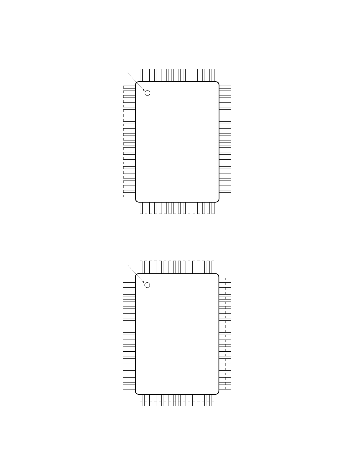
PIN #1 ID
VEEGND
80
79
EHCLKSE
ECLGND
78
77NC76NC75
STRBOUT
LOCKED
MDFSEL
74
M20SEL
GND
73
72
FLAGSEL
DAV*
71
70
CAV*FFED
69
68
67
ECLGND
RFD
66
65
1
CAP0B
2
CAP0A
3
CAP1A
CAP1B
4
5
6
HGND
7
8
STRBIN
9
STRBIN*
HCLKON
HCLK
HCLK*
HGND
LOUT
LOUT*
LOOPEN
DOUT
DOUT*
DIV0
DIV1
V
V
GND
GND
10
11
12
13
14
15
16
17
18
19
20
21
EE
22
EE
23
24
252627282930313233343536373839
INV
DATECODE
LOT# Tx
NCNCNCNCNCNCNC
HDMP-1012
HP
D19
D18
D17
RST*
D16
D15
40
D14
ECLGND
Figure 8. HDMP-1012 (Tx) Package Layout, Top View.
64
GND
63
GND
62
V
EE
V
61
EE
60
FLAG
59
D0
D1
58
57
D2
56
D3
55
D4
54
D5
53
D6
52
GND
51
D7
50
D8
49
D9
48
D10
47
D11
46
D12
D13
45
44
GND
GND
43
42
V
EE
41
V
EE
PIN #1 ID
CAP0B
CAP0A
CAP1A
CAP1B
GND
DIV0
DIV1
BCLK*
BCLK
TCLKSEL
TCLK*
TCLK
HGND
DIN*
DIN
LOOPEN
LIN*
LIN
EQEN
FDIS
V
V
GND
GND
VEEPH1
GND
TEMP
NCLK
FCLK
VEEGND
ECLGNDD0D1D2D3D4D5
80
79
78
77
76
75
74
73
72
71
70
69
1
2
3
4
5
6
7
8
9
10
11
12
13
14
15
16
17
18
19
20
21
EE
22
EE
23
24
252627282930313233343536373839
ACTIVE
STAT1
STAT0
DATECODE
LOT# Rx
EE
V
M20SEL
SMRST1
SMRST2
HDMP-1014
HP
GND
ECLGND
FLAGSEL
STRBOUT
LINKRDY*
68
DAV*
67
CAV*
66
FF
D6
65
40
ERROR
64
63
62
61
60
59
58
57
56
55
54
53
52
51
50
49
48
47
46
45
44
43
42
41
GND
GND
V
EE
V
EE
D7
D8
D9
D10
D11
D12
D13
ECLGND
ECLGND
D14
D15
D16
D17
D18
D19
FLAG
GND
GND
V
EE
V
EE
586
Figure 9. HDMP-1014 (Rx) Package Layout, Top View.

Tx I/O Definition
Name Pin Type Signal
CAP0A 2 C Loop Filter Capacitor: CAP0A should be shorted to CAP0B. CAP1A
CAP0B 1 should be shorted to CAP1B. A loop filter capacitor of 0.1 µF must be
CAP1A 3 connected across the CAP0 and CAP1 inputs to increase the loop time
CAP1B 4 constant.
CAV* 69 I-ECL Control Word Available Input: This active-low input tells the chip
that the user is requesting a control word be transmitted. This pin
should only be asserted after the user has determined the RFD line is
active for a given frame cycle. When this pin is asserted, the
information on the Data inputs is sent as a control frame. If CAV and
DAV are asserted simultaneously, CAV takes precedence.
D0 59 I-ECL Data Inputs: 20 Bit data is encoded and transmitted when M20SEL
D1 58 is active; otherwise the 16 least significant bits are encoded and
D2 57 transmitted. The encoded bits are transmitted LSB first. (e.g.: D0 is
D3 56 sent first, through to either D15 or D19, followed by the 4 coding bits
D4 55 C0-C3.)
D5 54
D6 53
D7 51
D8 50
D9 49
D10 48
D11 47
D12 46
D13 45
D14 40
D15 39
D16 38
D17 37
D18 36
D19 35
DAV* 70 I-ECL Data Available Input: This active-low input tells the chip that the
user has valid data to be transmitted. This pin should be asserted only
after the user has determined that the RFD line is active for a given
frame cycle. When this pin is asserted, the information on the Data
and Flag inputs is encoded and sent as a Data frame.
DIV0 19 I-ECL VCO Divider Select: These two pins program the VCO divider chain
DIV1 20 to operate at full speed, half speed, quarter speed or one-eighth speed.
DOUT 17 O-BLL Normal Serial Data Output: Output used when LOOPEN is not
DOUT* 18 active. This output is a special buffer line logic driver, which is a 50 Ω
back-terminated ECL compatible output.
ECLGND 33 S ECL Ground: Normally 0 volts. This ground is used for the ECL pad
66 drivers. For best performance, coupling of the noisy ECLGND to the
77 clean GND and HGND grounds be minimized.
ED 67 I-ECL Enable Data: This signal comes from the Rx chip state machine and
is used to control the RFD output of the Tx chip. The state machine
only allows data to be enabled when both sides of the link have
established stable lock.
587

Tx I/O Definition (cont’d.)
Name Pin Type Signal
EHCLKSEL 78 I-ECL EHCLK Enable: When active, this input causes the STRBIN inputs
to be used for the transmit serial clock, rather than the internal VCO
clock. This is useful for generating extremely low jitter test signals, or
for operating the link at speeds that are not within the VCO range.
When the STRBIN is active, it is necessary for the data source to take
its clock from the link rather than the usual operation where the Link
phase-locks onto the data source clock.
FF 68 I-ECL Fill Frame Select: When neither CAV or DAV is asserted, or when
ED is false, fill frames are automatically transmitted to allow the Rx
chip to maintain lock. The type of fill frame sent is determined by
the state of this pin. FF0s are sent if low, and either FF1a or FF1b is
sent if FF is high. The choice of FF1a and FF1b is determined by the
state of the cumulative line DC balance.
FLAG 60 I-ECL Extra Flag Bit: When FLAGSEL is active, this input is sent as an
extra data bit in addition to the normal Data inputs. When FLAGSEL
is not asserted, this input is ignored and the transmitted Flag bit is
internally alternated to allow the Rx chip to perform enhanced frame
error detection.
FLAGSEL 71 I-ECL Flag Bit Mode Select: When this input is high, the extra FLAG bit
input is sent as an extra transparent data bit. Otherwise, the FLAG
input is ignored and the transmitted flag bit is internally alternated
by the transmitter. The Rx chip can provide enhanced frame error
detection by checking for strict alternation of the flag bit during data
frames. The FLAGSEL input on the Rx chip should be set to the same
value as the Tx FLAGSEL input.
GND 23 S Ground: Normally 0 volts. This ground is used for everything other
24 than the noisy ECL outputs.
43
44
52
63
64
72
79
HCLK 11 O-BLL High Speed Clock Monitor: Used to monitor actual clock signal
HCLK* 12 used to transmit the serial data. This signal will either be the divided
VCO output, or the divided EHCLK external clock input, depending
on the value of the EHCLKSEL input.
HCLKON 10 I-ECL HCLK Power-down Control: When this pin is de-asserted, the
HCLK, HCLK* outputs are powered down to reduce power
dissipation.
HGND 7 S High Speed Ground: Normally 0 volts. This ground is used to
13 provide a clean reference for STRBIN and STRBIN* inputs. For
optimum impedance matching, it is suggested that the physical
distance between this pin and the ground plane be minimized.
588

Tx I/O Definition (cont’d.)
Name Pin Type Signal
INV 25 O-ECL Invert Signal: A high value of INV implies that the current frame is
being sent inverted to maintain long-term DC balance. With a buffer,
or pulled down with a 1K resistor to VEE and ac coupled, this signal
is useful as an aid to analyzing the serial output stream with an
oscilloscope.
LOCKED 75 O-ECL Loop In-lock Indication: This signal indicates the lock status of the
Tx PLL. A high value indicates lock. This signal is normally connected
to the SMTRST1 reset input of the Rx state machine to force the link
into the start-up state until the Tx PLL has locked. This signal may
give multiple false-lock indications during the acquisition process, so
should be debounced if it is used for any other purpose than to drive
the Rx chip.
LOOPEN 16 I-ECL Loop Back Control: Input which controls whether the DOUT,
DOUT*, or the LOUT, LOUT* outputs are currently enabled. If active,
LOUT, LOUT* are enabled. The unused output is powered down to
reduce dissipation.
LOUT 14 O-BLL Loop Back Serial Data Output: Output used when LOOPEN is
LOUT* 15 active. Typically this output will be used to drive the LIN, LIN* inputs
of the Rx chip.
M20SEL 73 I-ECL 16 or 20 Bit Word Select: When this signal is high, the link operates
in 20 Bit data transmission mode. Otherwise, the link operates in
16 Bit mode.
MDFSEL 74 I-ECL Select Double Frame Mode: When this signal is high, the PLL
expects a 1/2 speed parallel clock at STRBIN. The chip then internally
multiplies this clock and produces a full-rate parallel clock at
STRBOUT. Note that the phase relationship of STRBIN to STRBOUT
and the sampling point change with asserting MDFSEL, as shown in
the Tx timing diagram. This feature is provided so that either a 40 bit
or 32 bit word can be easily transmitted as two 20, or two 16 bit
words. When MDFSEL is low, the PLL expects a full-rate parallel
clock at STRBIN.
RFD 65 O-ECL Ready for Data: Output to tell the user the Link is ready to
transmit data. This pin is a retimed version of the ED input, which is
driven by the Rx chip state machine controller.
RST* 34 I-ECL Chip Reset: This active-low pin initializes the internal chip registers.
It should be asserted during power up for a minimum of 5 parallelrate clock cycles to ensure a complete reset.
STRBIN 8 I-H50 Data Clock Input: When EHCLKSEL is low, this input is phase
STRBIN* 9 locked and multiplied to generate the high speed serial clock. The chip
expects a clock frequency which is equal to the input frame rate if
MDFSEL (double frame mode) is low, and 1/2 the frame rate if
MDFSEL is high. When EHCLKSEL is high, the PLL is bypassed,
and STRBIN directly becomes the high speed serial clock. Refer to
the Tx Timing diagram for the phase relationship between STRBIN,
data and STRBOUT.
589

Tx I/O Definition (cont’d.)
Name Pin Type Signal
STRBOUT 76 O-ECL Frame-rate Data Clock Output: This output is always a frame rate
clock derived from STRBIN. With a buffer or pulled down with a 1K
resistor to VEE and ac- coupled, this output is ideal for triggering an
oscilloscope for examining the serial output eye pattern DOUT or
LOUT.
V
EE
21 S Power: Normally -5 V ± 10%.
22
41
42
61
62
80
590

Rx I/O Definition
Name Pin Type Signal
ACTIVE 25 I-ECL Chip Enable: This input is normally driven by the Rx state machine
output. The ACTIVE signal is internally retimed by STRBOUT and
presented to the user as the LINKRDY signal. This is how the Rx
state machine signals the user that the start-up sequence is complete.
BCLK 9 O-BLL VCO Monitor Output: These pins provide access to the internal
BCLK* 8 VCO clock.
CAP0A 2 C Loop Filter Capacitor: CAP0A should be shorted to CAP0B. CAP1A
CAP0B 1 should be shorted to CAP1B. A loop filter capacitor of 0.1 µf must be
CAP1A 3 connected across the CAP0 and CAP1 inputs to increase the loop time
CAP1B 4 constant.
CAV* 38 O-ECL Control Frame Available Output: This active-low output indicates
that the Rx chip data outputs are receiving Control Frames. False
CAV indications may be generated during link startup.
D0 71 O-ECL Data Outputs: 20 Bit data is received and decoded when M20SEL is
D1 70 active; otherwise 16 bit data is decoded and the D16-D19 bits
D2 69 are undefined.
D3 68
D4 67
D5 66
D6 65
D7 60
D8 59
D9 58
D10 57
D11 56
D12 55
D13 54
D14 51
D15 50
D16 49
D17 48
D18 47
D19 46
DAV* 37 O-ECL Data Available Output: This active-low output indicates that the
Rx chip data outputs, D0..D19, have received data frames. Data
should be latched on the rising edge of STRBOUT. Note that during
link startup, false data indications may be given. The DAV* and
LINKRDY outputs can be used together to avoid confusion during
link startup.
DIN 15 I-H50 Normal Serial Data Input: This is the input used when LOOPEN
DIN* 14 is not active. When LOOPEN is high, the loop back data inputs LIN,
LIN* are used instead. An optional cable equalizer may be enabled for
the DIN, DIN* inputs by asserting EQEN.
DIV0 6 I-ECL VCO Divider Select: These two pins program the VCO divider chain
DIV1 7 to operate at full speed, half speed, quarter speed or one-eighth speed.
591

Rx I/O Definition (cont’d.)
Name Pin Type Signal
ECLGND 32 S ECL Ground: Normally 0 volts. This ground is used for the ECL pad
52 drivers. For best performance it is suggested that coupling of the noisy
53 ECLGND to the clean GND and HGND grounds be minimized.
72
EQEN 19 I-ECL Enable Input for Cable Equalization: When asserted, this signal
activates the cable equalization amplifier on the DIN, DIN* serial
data inputs.
ERROR 40 O-ECL Received Data Error: Asserted when a frame is received that does
not correspond to either a valid Data, Control, or Fill frame encoding.
When FLAGSEL is not active, the Rx chip also tests for strict
alternation of flag bits during data frames. A flag bit alternation
error will also cause an ERROR indication.
FCLK 75 O-ECL Frame Clock Monitor: Leave unterminated in normal use.
FDIS 20 I-ECL Frequency Detector Disable Input: When active, this input
disables the Rx PLL Frequency detector and enables a phase detector.
The Frequency detector is used during the start-up sequence to
acquire wide-band lock on Fill Frames, but must be disabled prior to
sending data patterns. This input is normally controlled by the Rx
state machine.
FF 39 O-ECL Fill Frame Status: During a given STRBOUT clock cycle, if neither
DAV, CAV, or ERROR are active, then the currently received frame
is a Fill frame. The type of fill frame received is indicated by the FF
pin. If FF is low, then FF0 has been received. If FF is high, then
either FF1a or FF1b has been received.
FLAG 45 O-ECL Flag Bit: If both Tx and Rx have FLAGSEL asserted, this output
indicates the value of the transmitted flag bit, then this received bit
can be treated just like an extra data bit. If both Tx and Rx have
FLAGSEL set to low, FLAG is used to differentiate the even frame
from the odd frame in the line code.
FLAGSEL 34 I-ECL Flag Bit Mode Select: When this input is high, the extra FLAG bit
output is effectively an extra transparent data bit. Otherwise, the
FLAG bit is checked for alternation during data frames. Any break in
strict alternation results in an ERROR indication to the user.
GND 5 S Ground: Normally 0 volts. This ground is used for all the core logic
23 other than the output drivers.
24
33
43
44
63
64
73
78
HGND 13 S High Speed Ground: Normally 0 volts. This ground is used to
provide clean references for the high speed DIN, DIN*, LIN, LIN*,
TCLK, TCLK* inputs.
592

Rx I/O Definition (cont’d.)
Name Pin Type Signal
LIN LIN* 18 I-H50 Loop Back Serial Data Input: Use this input when LOOPEN is
17 active. Unlike the DIN, DIN* inputs, this input does not have a cable
equalizer. In normal usage, this input will be connected to the Tx
chip LOUT, LOUT* outputs. This allows the user to check the
near-end functionality of the Tx and Rx pair independent of the
transmission medium
LOOPEN 16 I-ECL Loop Back Control: When asserted, this signal causes the loop back
data inputs LIN, LIN* to be used instead of the normal data inputs
DIN, DIN*.
LINKRDY* 36 O-ECL Link Ready Indicator: This active-low output is a retimed version
of the ACTIVE input. ACTIVE is normally driven by the Rx state
machine output. LINKRDY* then indicates that the startup sequence
is complete and that the data and control indications are valid.
M20SEL 30 I-ECL 16 or 20 Bit Word Select: When this signal is high, the link operates
in 20 Bit data reception mode. Otherwise, the link operates in 16 Bit
mode and data outputs D16-D19 are undefined.
NCLK 76 O-ECL Nibble Clock Monitor: Leave unterminated in normal use.
TEMP 77 T Temperature Sense Diode: Used during wafer and package test
only. It should be left open.
PH1 79 O-ECL Phase Detector Test Output: The output from the phase/frequency
detector in the Rx PLL. When PH1 is high, the VCO should increase
frequency. When low, the VCO should decrease frequency.
SMRST0* 28 I-ECL State Machine Reset Inputs: Each of these active-low input pins
SMRST1* 29 reset the Rx state machine to the initial start-up state. This initiates
a complete PLL restart and handshake at both ends of the duplex
link. Normally, SMCRST0* is connected to a power-up reset circuit
or a host system reset signal. The SMCRST1* input is normally
connected to the Tx LOCKED output. The LOCKED signal holds the
state-machine in the start-up state until the Tx PLL is locked.
STAT0 27 O-ECL State Machine Status Outputs: These outputs indicate the current
STAT1 26 state-machine state. They are used to directly control the Tx ED,
Tx FF, Rx FDIS, and Rx ACTIVE lines.
STRBOUT 35 O-ECL Recovered Frame-rate Data Clock Output: This output is the PLL
recovered frame rate clock. D0-D19, FLAG, DAV, CAV, FF, LINKRDY,
and ERROR should all be latched on the rising edge of STRBOUT.
TCLK 12 I-H50 External VCO Replacement Test Clock: When TCLKSEL in
TCLK* 11 enabled, this input is used in place of the normal VCO signal,
effectively disabling the PLL and allowing the user to provide an
external retiming clock for testing.
TCLKSEL 10 I-ECL Enable Test Clock Input: When this input is active, the TCLK,
TCLK* inputs are used in place of the normal VCO signal. This
feature is useful both for synchronous systems and for chip testing.
593

Rx I/O Definition (cont’d.)
Name Pin Type Signal
V
EE
21 S Power: Normally -5 V +10%
22
31
41
42
61
62
74
80
594

Mechanical Dimensions and Surface Mount Assembly Recommendations
Both the HDMP-1012 and HDMP1014 are implemented in an
industry standard M-Quad 80
package. The package outline
dimensions conform to JEDEC
plastic QFP specifications and are
shown below in Figure 10. The MQuad 80 package material is
aluminum and the leads have
been formed into a “Gull-Wing”
configuration for surface
mounting.
M-Quad 80 Package Information
Item Details
Package Material Aluminum
Lead Finish Material 85/15 Sn/Pb
Lead Finish Thickness 300 - 600 µ inches
Lead Coplanarity 0.004 inches maximum
PIN #1 ID
We recommend keeping the
package temperature, Tc, below
75°C. Forced air cooling may be
required.
+0.18
19.786
-0.08
+0.008
TOP VIEW
+0.16
13.792
-0.04
+0.008
-0.002
)
(0.543
17.20 ± 0.10
(0.677 ± 0.004)
ALL DIMENSIONS ARE IN MILLIMETERS (INCHES).
(0.779
(0.104 ± 0.005)
-0.002
23.20 ± 0.10
(0.913 ± 0.004)
2.64 ± 0.13
)
Figure 10. Mechanical Dimensions of HDMP-1012 and HDMP-1014.
0.35 TYP.
(0.014 TYP.)
0.80 TYP.
(0.0315 TYP.)
7 DEG
0.38 ± 0.05
(0.015 ± 0.002)
0.15
(0.006)
0.80 ± 0.13
(0.031 ± 0.005)
595

Appendix I: Additional Internal Architecture Information
Line Code Description
The HDMP-1012/1014 line code
is Conditional Invert Master
Transition (CIMT), illustrated in
Figure 11. The CIMT line uses
three types of frames: data
frames, control frames, and fill
frames. Fill frames are internally
generated by the Tx chip for use
during link start up and when
there is no input from the user.
DATA FIELD
SERIAL
DATA
16/20 BITS
Each frame consists of a Data
Field (D-Field) followed by a
Coding Field (C-Field). The DField can be either 16-bits or 20bits wide, depending on link
configuration. The C-Field has a
master transition which serves as
a fixed timing reference for the
receivers clock recovery circuit.
Users can send arbitrary data
carried by Data or Control
Frames. The dc balance of the
line code is automatically
enforced by the Tx. Fill frames
have a single rising edge at the
CODING FIELD
4 BITS
master transition which is used
for clock recovery and frame
synchronization at the receiver.
Detailed coding schemes are
described in the following
subsections. All the tables given
in this section show data bits in
the same configuration as a scope
display. In other words, the
leftmost bit in each table is the
first bit to be transmitted in time,
while the rightmost bit is the last
bit to be transmitted.
MASTER
TRANSITION
FILL
FRAME
FRAME K
Figure 11. HDMP-1012/1014 (Tx/Rx Pair) Line Code.
Data Frame Codes
When not in FLAGSEL mode, the
FLAG bit is not user controllable
and is alternately sent as 0 and 1
by the Tx chip during data frames
to provide enhanced error
detection. Control and Fill frames
do not cause toggling between
even and odd frames to occur
(The FLAG bit is not available
during control frames). The
receiver performs a differential
detection to make sure that every
data frame received is the
opposite pattern from the
previous frame. If a break in the
frame error is flagged by
asserting the Rx ERROR output.
This pattern detection makes it
impossible for a static input data
pattern to generate an
undetectable false lock point in
the transmitted data stream. The
detection also reduces the
probability that the loop could
lock onto random data at a point
away from the true master
transition for any significant time
before it would be detected as a
false lock. This mode can detect
all single-bit errors in the C-field
(non-data bit fields) of the frame.
strict alternation is observed, a
FRAME K+1
When the chip is in FLAGSEL
mode, the extra FLAG bit is freely
user definable as an extra data
bit. This provides a 17th bit in 16
bit mode, and a 21st bit in 20 bit
mode. The probability of
undetected false lock is higher,
but the users (e.g., SCI-FI) that
need the extra bit can detect false
lock at a higher level of the
network protocol with clock
recovery circuits, etc. If the
higher level protocols consistently
receive wrong data, they can
initiate a link restart by resetting
the Rx state machine.
596

HDMP-1012 (Tx), HDMP-1014 (Rx)
Operating Modes
M20SEL FLAGSEL Description
0 0 16 bit data plus error checking
0 1 16 bit data plus FLAG
1 0 20 bit data plus error checking
1 1 20 bit data plus FLAG
HDMP-1012 (Tx), HDMP-1014 (Rx)
Data Frame Structure
M20SEL Not Asserted (16 bit data mode)
Data Status Flag bit D-Field C-Field
True 0 D0 - D
Inverted 0 D0 - D
True 1 D0 - D
Inverted 1 D0 - D
15
15
15
15
HDMP-1012 (Tx), HDMP-1014 (Rx)
Data Frame Structure
M20SEL Asserted (20 bit data mode)
1101
0010
1011
0100
Data Status Flag bit D-Field C-Field
True 0 D0 - D
Inverted 0 D0 - D
True 1 D0 - D
Inverted 1 D0 - D
Control Frame Codes
There are 218 control words
provided in 20 bit mode. If the
user desires to send a control
word, his lower 9 bits (D0-D8)
are sent as bits D0-D8 of the DField. The user’s next 9 bits (D9-
D17) are sent as bits D11-D19 of
the D-Field. The control frame is
either inverted or not inverted as
needed to maintain balance, with
the coding bits 0011 used to
indicate true control, and the bits
1100 used to indicate
complement control. The bits d9
and d10 are always forced to 0 1
19
19
19
19
for true control frames and 1 0
1101
0010
1011
0100
for complement control frames.
These middle bits are used to
distinguish control frames from
fill frames, which always have the
middle bits set to either 00, 11, or
10. Similarly, there are 2
14
control words provided in 16 bit
mode.
597

HDMP-1012 (Tx), HDMP-1014 (Rx)
Control Frame Structure
M20SEL Not Asserted (16 bit mode)
D-Field C-Field
D0 - D6 D7 D8 D9 - D15 C0 C1 C2 C3
D0 - D
D
- D
0
6
6
01D
10D
- D
7
- D
7
13
13
0011
1100
HDMP-1012 (Tx), HDMP-1014 (Rx)
Control Frame Structure
M20SEL Asserted (20 bit mode)
D-Field C-Field
D0 - D8 D9 D10 D11-D19 C0 C1 C2 C3
D0 - D80 1 D
D0 - D81 0 D
-D170011
9
-D171100
9
Fill Frame Codes
Two logical fill frames are
provided: FF0 and FF1. FF0 is
physically a 50% duty cycle wave
form with its sole rising edge
occurring between C1 and C2.
Logical FF1 toggles between two
different physical codes, the first
of which advances the falling edge
of FF0 by one bit, the second of
HDMP-1012 (Tx), HDMP-1014 (Rx)
Fill Frame Structure
M20SEL Not Asserted (16 bit mode)
Fill Frame D-Field C-Field
0 1111111 10 0000000 0011
1a 1111111 11 0000000 0011
1b 1111111 00 0000000 0011
HDMP-1012 (Tx), HDMP-1014 (Rx)
Fill Frame Structure
M20SEL Asserted (20 bit mode)
Fill Frame D-Field C-Field
0 111111111 10 000000000 0011
1a 111111111 11 000000000 0011
1b 111111111 00 000000000 0011
which retards the falling edge of
FF0 by one bit. Two logical fill
frame types are required for link
start up in duplex mode.
598

HDMP-1014 (Rx)
Detectable Error States
M20SEL Not Asserted (16 bit mode)
D-Field C-Field
xxxxxxx xx xxxxxxx x00x
xxxxxxx xx xxxxxxx x11x
xxxxxxx 0x xxxxxxx 1100
xxxxxxx 11 xxxxxxx 1100
xxxxxxx xx xxxxxxx 1010
xxxxxxx xx xxxxxxx 0101
HDMP-1014 (Rx)
Detectable Error States
M20SEL Asserted (20 bit mode)
D-Field C-Field
xxxxxxxxx xx xxxxxxxxx x00x
xxxxxxxxx xx xxxxxxxxx x11x
xxxxxxxxx 0x xxxxxxxxx 1100
xxxxxxxxx 11 xxxxxxxxx 1100
xxxxxxxxx xx xxxxxxxxx 1010
xxxxxxxxx xx xxxxxxxxx 0101
Tx Operation Principles
The HDMP-1012 (Tx) is implemented in a high performance
silicon bipolar process. The Tx
performs the following functions
for link operation:
• Phase lock to frame rate clock
• Clock multiplication
• Frame encoding
• Multiplexing
In normal operation, the Tx phase
locks to a user supplied frame
rate clock and multiplies the
frequency to produce the high
speed serial clock. When locked,
the Tx indicates that it is locked
by asserting the LOCKED output.
When the ED input is asserted,
the Tx asserts the RFD signal
indicating that it is now ready to
transmit data or control frames.
The Tx can accept either 16 or 17
bit wide parallel data and produce
a 20 bit frame. It also can accept
20 or 21 bit data and produce a
24 bit frame. Similarly, either 14
bit or 18 bit control words can be
transmitted in a 20 bit or 24 bit
frame respectively.
Tx Encoding
A simplified block diagram of the
transmitter is shown in Figure 4.
The PLL/Clock Generator locks
onto the incoming frame rate (or
one-half frame rate) clock and
multiplies it up to the serial clock
rate. It also generates all the
internal clock signals required by
the Tx chip.
The data inputs, D0-D19, as well
as the control signals; ED, FF,
DAV*, CAV*, and FLAG are
latched in on the rising edge of an
internally generated frame rate
clock. The data field is then
encoded depending on the state
of the control signals. At the same
time, the coding field is
generated. At this point, the entire
frame has been constructed in
parallel form and its sign is
determined. This frame sign is
compared with the accumulated
sign of previously transmitted bits
to decide whether to invert the
frame. If the sign of the current
frame is the same as the sign of
the previously transmitted bits,
then the frame is inverted. If the
signs are opposite, the frame is
not inverted. No inversion is
599

performed if the frame is a fill
frame.
The Output Select block allows
the user to select between two
sets of differential high speed
serial outputs. This feature is
useful for loop back testing. If
LOOPEN is high, LOUT is enabled
and DOUT is disabled. If LOOPEN
is low, DOUT is enabled and
LOUT is disabled.
The active-low RST* input resets
the internal registers to a
balanced state. This pin should be
held low for at least five frame
rate clock cycles to ensure a
complete reset.
The Data Field and Control Field
are encoded depending on ED,
FF, DAV*, CAV*, FLAG,
FLAGSEL, M20SEL as well as two
internally generated signals, O/E
and ACCMSB.
When FLAGSEL is high, O/E is
equivalent to FLAG. This is
equivalent to adding an additional
bit to the data field. When
FLAGSEL is low, O/E alternates
between high and low for data
frames. This allows the link to
perform more extensive error
detection when the extra bit is
unused.
ACCMSB is the sign of the
previously transmitted data. This
is used to determine which type of
FF1 should be sent. When
ACCMSB is low, FF1a is sent and
when ACCMSB is high, FF1b is
sent. This effectively drives the
accumulated offset of transmitted
bits back toward the balanced
state.
Tx Phase-Locked Loop
The block diagram of the
transmitter phase-locked loop is
shown in Figure 12. It consists of
a sequential frequency detector,
loop filter, VCO, clock generation
circuitry, and a lock indicator.
The outputs of the frequency
detector pass through a charge
pump filter that controls the
center frequency of the VCO.
These outputs also go to the VCO
directly to effectively add a zero
in the loop response. An external
high-speed clock can be used
instead of the VCO clock. This is
accomplished by applying a high
signal to EHCLKSEL and a
differential clock to STRBIN.
One of four frequency bands may
be selected by applying
appropriate inputs to DIV0 and
DIV1. The VCO or STRBIN
frequency is divided by N, where
N is 1, 2, 4, or 8 corresponding to
the binary number represented by
DIV1, DIV0. This divided version
of the VCO clock or STRBIN is
used as the serial rate clock and is
available as a differential signal at
the HCLK output.
A clock generator block creates
all the clock signals required for
the chip. Depending on M20SEL,
STRBOUT is either HCLK/20 or
HCLK/24. If MDFSEL is low, then
STRBOUT is a phase-locked
version of STRBIN. If MDFSEL is
high, STRBOUT is twice the
frequency of STRBIN.
STRBIN
M20SEL
MDFSEL
Figure 12. HDMP-1012 (Tx) Phase-Locked Loop.
FREQ
DETECT
INTERNAL CLOCKS
CLOCK
GENERATOR
LOCK
DETECT
LOCKED
STRBOUT
600
HCLK
FILTER
DIV N
DIV0 DIV1
VCO
0
STRBIN1
EHCLKSEL

The lock detect circuit samples
STRBIN with phase shifted
versions of STRBOUT. If the
samples are not the proper
values, the LOCKED signal goes
low and stays low for at least two
frames.
Rx Operation Principles
The HDMP-1014 (Rx) is
monolithically implemented in a
high performance 25 GHz f
t
bipolar process. When properly
configured, the Rx can accept
20B/24B CIMT line code frames,
and then output parallel 16B/17B/
20B/21B Data Word or 14B/18B
Control Word. The Rx provides
the following functions for link
operation:
• Clock recovery
• Frame synchronization
• Data recovery
• Demultiplexing
• Frame decoding
• Frame error detection
• Link state control
Rx Encoding
Figure 5 shows a simplified block
diagram of the receiver. The data
path consists of an Input Select,
an Input Sampler, a Frame
Demultiplexer, a Control Field (CField) Decoder, and a Data Field
(D-Field) Decoder. An on-chip
phase-locked loop (PLL) is used
to extract timing reference from
the serial input (DIN or LIN). The
PLL includes a Phase-Frequency
Detector, a Loop Filter, and a
variable-frequency oscillator
(VCO). All the RX internal clock
signals are generated from a
Clock Generator. The Clock
Generator can be driven either by
internal VCO or external signal,
TCLK, depending on the Clock
Select configuration.
Integrated on the chip is a LinkControl State Machine for link
status monitoring and link
startup. Figure 13 shows the
details of the Input Select. The
Input Select chooses either
nominal serial data (DIN) or
loopback (LIN) signal for the
Input Sampler’s input. If loopback
enable (LOOPEN) is asserted, the
LIN input is selected. Also
included in the Input Selector is
cable equalization circuitry. When
coaxial cable is used as the
transmission media, by setting
EQEN=1 (enable equalization),
the equalization circuitry is in the
DIN signal path and can
compensate for high-frequency
cable loss.
Because the Data Field of the
CIMT line code can be either 16bit or 20-bit wide, the width
selection for Rx is made by
setting the input pin M20SEL
(Figure 5). If M20SEL=1, then
the Rx is configured to accept
serial input with 20-bit data field,
i.e., 24 bits per frame. If M20SEL
= 0, 16-bit data field is selected.
LOOPEN
EQEN
DIN
CABLE EQ
LIN
Figure 13. HDMP-1014 (Rx) Input Selector.
HDMP-1014 (Rx) PhaseLocked Loop
A more detailed block diagram for
the Rx phase-locked loop (PLL) is
shown in Figure 14. In the PLL,
the phase of the serial input, SIN,
is compared with synchronizing
signals from the internal clock
generator, using either a phase
detector or a frequency detector.
The frequency detector disable
signal, FDIS, selects which
detector to use. If synchronization
in a link is not yet established, the
HDMP-1012 (Tx) should send out
Fill Frame 0 (FF0) or Fill Frame 1
(FF1) to the remote Rx. By
setting FDIS=0, the Rx uses
0
1
0
1
SIN
601
FDIS
FREQ
SIN
PHASE
STRBOUT
Figure 14. HDMP-1014 (Rx) Phase-Locked Loop.
the frequency detector to align its
internal clock with the rising edge
of FF0/FF1. Once frequency lock
CLOCK GEN
BCLK
4, 8 by setting DIV1, DIV0 = 00,
01, 10, 11 (see Operating Rate
Tables).
is accomplished, FDIS can be set
to 1, then the PLL uses only the
phase detector for
synchronization adjustment and
the Rx is ready to receive data.
Due to the narrow frequency
acquisition range of the phase
detector, the frequency detector
is used for internal frequency
acquisition. The frequency
detector, however, can only work
with FF0 and FF1 and it is
necessary for the PLL selecting
the phase detector (by setting
FDIS=1) before receiving any
random data.
HDMP-1014 (Rx)
Decoding
In Figure 5, the frame
demultiplexer de-serializes the
recovered serial data from the
Input Sampler, and outputs the
resulting parallel data one frame
at a time. Every frame is
composed of a 16-bit or 20-bit
Data Field (D-Field) and a 4-bit
Control Field (C-Field). The C-
Field, C0-C3, together with the
two center bits of the D-Field (D9
and D10 for 20 bit mode, D7 and
D8 for 16 bit mode) are then
decoded by the C-Field decoder to
The output of the phase-
frequency detector is externally
available through pin PHI. An
external clock source can also be
used (through pin TCLK) by
setting TCLKSEL=1. To broaden
the usable frequency range of the
chip, there is a programmable
divider before the clock
generator. The VCO or TCLK
frequency can be divided by 1, 2,
determine the content of the
frame. The D-Field decoder is
controlled by the outputs of the C-
Field decoder. If an inverted Data
Word or Control Word is
detected, the D-Field decoder will
automatically invert the D-Field
data. If a Control Frame is
detected, the D-Field decoder will
shift the bottom half of the D-
Field so that the outputs are at
0
1
DIV N
DIV0 DIV1
TCLKSEL
PH1
0
1
VCO
FILTER
TCLK
pin D0 - D17 (if M20SEL =1) or
at pin D0 - D13 (if M20SEL =0).
A data Frame is detected by the
receiver when DAV = 1. A control
Frame is detected by the receiver
if CAV = 1. A Fill Frame is
detected by the receiver if DAV =
0 and CAV = 0.
The C-Field decoder will set iERR
= 1 when it detects an error. The
internal error bit (iERR) is
combined with the internal flag
bit (iFLAG) and the flag-bit modeselect signal (FLAGSEL) to
produce the externally available
error bit (ERROR) and flag
(FLAG) bits. If FLAGSEL=1, the
FLAG can be used as an extra
data bit
• ERROR=iERR.
• FLAG=iFLAG.
• If a Fill Frame is detected, then
FLAG=0.
• If a Control Frame is detected,
FLAG should be ignored.
If FLAGSEL=0, the serial input is
assumed to consist of alternating
602

even frames (iFLAG=0) and odd
frames (iFLAG=1).
• If iERR=1, then ERROR=1.
• If a Fill Frame is detected, then
FLAG=0.
• If a Data Frame is detected,
then FLAG=iFLAG, and iFLAG
should alternate between 0 and
1, starting with 0 and ending
with 1; otherwise, ERROR=1.
• If a Control Frame is detected,
then FLAG automatically
alternates between 0 and 1,
starting with 0.
The even or odd feature allows a
32/40-bit wide data word to be
transmitted through the link. A
2:1 multiplexer and a 1:2 demultiplexer are required. FLAG is used
to synchronize the even and odd
frames. Note, both Data and
Control Frames can be
transmitted as even/odd pairs, but
only Data Frames can be detected
for out of order errors.
HDMP-1014 (Rx) LinkControl State Machine
Operation Principle
The link-control state machine
(SMC) on the Rx chip provides a
link handshake protocol enabling
the duplex link to transition from
frequency acquisition and training
mode into data mode.
The HDMP-1012/1014 Tx/Rx link
uses an explicit frequency
acquisition mode at startup that
operates on a square-wave
training sequence. This makes it
possible to use a VCO with a very
wide tuning range yet avoid the
harmonic false lock problems
associated with other circuits of
this type.
Using the SMC, a full duplex data
channel can be implemented
without additional controller or
hardware.
The State Machine Handshake Protocol
Figure 1d shows a simplified
block diagram of the HDMP1012/1014 data channel configured for full duplex operation.
Two HDMP-1012/1014 chipsets
are required to perform the
handshake in parallel. There are
three states that the link must go
through to complete the link
startup process:
• State 0: Frequency Acquisition
• State 1: Waiting for Peer
• State 2: Sending Data
Each side of the link decides
which of the three states that it
should be in. The decision is
based on its own past memory
and the type of frame that it is
currently receiving from the other
side of the link.
Considering only the local port of
the link, there is a transmitter
(Tx), a receiver (Rx) and a state
machine controller (SMC). The
SMC entity, although logically
distinct, is implemented on the
same die as the Rx chip. The SMC
monitors the data frame status
indicators (ERROR, DAV, CAV,
FW) from the Rx, and is able to
force (or control) various
characteristics of the Tx and the
Rx chips. The Tx chip has the
following controllable features:
• It can be forced to send a Fill
Frame using the ED input.
• The type of Fill Frame sent can
be controlled using the FF
input.
The Rx Chip has the following
controllable features:
• It can be in Frequency
acquisition or Phase-lock/Data
reception mode depending on
the state of the FDIS input.
• It can be enabled for data
reception or set in a mode in
which data frames are ignored
depending on the ACTIVE
input.
The Rx chip can also distinguish
between various types of frames.
It can also communicate the
frame type to the SMC. The
various frame types are:
• Fill Frame 0, (FF0)
• Fill Frame 1 a/b (FF1)
• Data/Control frames (Data)
• Error frames (ERROR)
The SMC can also be reset by
either the SMCRST0* or
SMCRST1* inputs. Usually one of
these inputs is used for power-on
reset, and the other is connected
to the Tx LOCKED output.
This holds the SMC in state 0 until
the transmitter PLL has locked.
Figure 15 shows the state
diagram of the SMC. The SMC is
debounced by allowing state
transitions to be made only after
at least 2 consecutive frames give
the same indication. This prevents
single bit errors from causing
false state transitions. In addition
to this debouncing mechanism,
when two consecutive ERROR or
Resets occur, a timer is enabled
forcing the SMC into state zero
for 128 frame times. Any
transition out of this initial state
can only occur after the link has
been error-free for 128 frames.
This prevents false transitions
from being made during the bitslipping that occurs in the initial
frequency acquisition of both the
Tx and Rx PLLs.
603

SEND FF0
0
DISABLE DATA TRANSMISSION
DISABLE DATA RECEPTION
FREQUENCY DETECTOR ON
DATA
ERROR
RESET
FF1
FF0
FF0
ERROR
RESET
1
2
Figure 15. HDMP-1014 (Rx) State Machine State Diagram.
When the local port is in State 0,
it is in the reset state, where both
local Tx and Rx parallel interfaces
are disabled. The local Tx
SEND FF1
DISABLE DATA TRANSMISSION
ENABLE DATA RECEPTION
FREQUENCY DETECTOR OFF
DATA
FF1
SEND FF0
ENABLE DATA TRANSMISSION
ENABLE DATA RECEPTION
FREQUENCY DETECTOR OFF
phase detection mode. Parallel
data can be sent by the local Tx,
and at the same time, received by
the local Rx.
transmits FF0 continuously, and
the local Rx PLL is in the
frequency detection mode. When
the local Rx is phase-locked to the
remote Tx, it transitions to State
1. The local Tx transmits FF1 to
acknowledge the phase-locked
condition (its parallel input is still
disabled). The local Rx PLL is in
the phase detection mode and its
parallel output is enabled. When
in State 2, the two-way
synchronization between the local
port and the remote port is
established. Both local Tx and Rx
The Rx chip has the state machine
logic built in. The SMC has two
status outputs, STAT0 and STAT1,
that control the various features
of the two chips depending on the
current state. The TX inputs that
need to be controlled are FF and
ED. The RX inputs that need to be
controlled are FDIS and ACTIVE.
To control the chips as shown in
the state diagram of Figure 15,
the following interchip
connections must be made
(Figure 16):
parallel interfaces are enabled,
and the local Rx PLL is in the
ERROR
RESET
FF0
DATA
FF1
• Tx FF is driven by STAT1
• Tx ED is driven by STAT0
• Rx FDIS is driven by STAT1
• Rx ACTIVE is driven by STAT1
• TX RST and RX SMCRST0 are
driven by a power-on, or user,
reset circuit.
604

Tx DATA
INTERFACE
RST*
POWER-ON
RESET
Rx DATA
INTERFACE
Figure 16. Full Duplex Configuration.
SMCRST0*
LOCKEDEDFF
STAT0
STAT1
SMCRST1*
FDIS
ACTIVE
DOUT
LOUT
OPTIONS
LIN
DIN
DIN
LIN
OPTIONS
LOUT
DOUT
RxTx
ACTIVE
FDIS
TxRx
STAT1
STAT0
FF
ED
SMCRST1*
SMCRST0*
RST*
LOCKED
Rx DATA
INTERFACE
POWER-ON
RESET
Tx DATA
INTERFACE
Appendix II: Link Configuration Examples
This section shows some
application examples using the
HDMP-1012/1014 chipset. Refer
to I/O Definition for detailed
circuit-level interconnection.
This guide is intended to aid the
user in designing G-LINK into a
system. It provides the necessary
details of getting the system up,
without the detailed description of
the inner circuitry of the chip set.
The first section is a description
of the various configurations for
duplex and simplex operation.
The second section describes the
interface to both single frame and
double frame mode. Following
that is a section on the integrating
capacitor and power supply
bypassing recommendations.
Next is a guide to the various
types of electrical I/O
connections. The final section is a
discussion on TTL translations
and the use of a single positive
supply. Also included is a list of
the various options and their
definitions.
Duplex/Simplex Configurations
The following describes the
common setups for the link. In all
cases, the DIN and LIN are
differential high speed lines, and
unused leads should be
terminated with 50 Ω AC coupled
to ground. Since the data stream
has no DC component, a coupling
cap of 0.1 µF is recommended for
the DIN and LIN inputs.
Full Duplex
Figure 16 shows HDMP-1012/
1014 in a full duplex configuration connecting two bidirectional
(parallel) buses. Each end of the
link has a Tx and RX pair. The
receiver’s state machine outputs
(STAT0 and STAT1) are used to
control the status of the link.
Various options such as 16/20 bit
mode (M20SEL) and speed
selections (DIV0,DIV1) are
grouped together under the label
‘options’. A power-on reset is
available to the user to reset the
link during startup
Since the outputs STAT0 and
STAT1 are ECL levels, they can
be tied directly to the pins shown.
When the Tx has acquired lock to
the incoming STRBIN at the
frame rate, the LOCKED pin is
activated, which enables the Rx.
At this state, both STAT0 and
STAT1 are low, forcing the Tx to
send FF0, which is a square wave
pattern used by the remote Rx to
acquire frame lock. When the
local Rx has acquire frame lock,
STAT1 is set high to first turn off
its own frequency detector
(FDIS), then sets itself to active
mode (ACTIVE), and tells the
local Tx to send FF1 to signal the
remote Rx that the local pair is
ready. Likewise, when the remote
pair is ready, the local Rx will
605

receive FF1, causing STAT0 to go
high, which asserts the enable
data (ED) pin on the Tx. The ED
signal is retimed to signify to the
host that the Tx is ready to send
data (RFD). Other configurations
for duplex mode are also possible
with external user-defined state
machines. Simplex operation
using G-LINK is also possible. The
following sections discuss three
different types of simplex
configurations.
Simplex Method I. Simplex with Low-Speed Return Path
Low-speed lines are used in the
simplex method of Figure 17a.
The remote Rx controls the states
of both the Rx and the local Tx
using these low speed lines. This
is ideal for cases where these noncritical lines are available. Again,
a power on reset is available to
the user. This connection between
the Tx and Rx is identical to one
side of the duplex configuration.
When the Tx is locked, the Rx is
enabled via the LOCKED line. The
Rx’s STAT0 and STAT1 outputs
are low, causing the local Tx to
send FF0. When the Rx is frame
locked, STAT1 is raised, which
disables its frequency detector,
sets itself to active mode, and tells
Tx to send FF1. Upon receiving
FF1 from the Tx, the Rx’s STAT0
line is raised, which enables the
Tx (ED) for data transmission. If
desired, the Rx reset pin
(SMCRST1) can be tied high, and
Tx DATA
INTERFACE
POWER-ON
RESET
Tx DATA
INTERFACE
POWER-ON RESET
PERIODIC
SYNC PULSES
Tx DATA
INTERFACE
POWER-ON
RESET
DOUT
LOUT
RST*
LOCKEDEDFF
OPTIONS
DOUT
LOUT
OPTIONS
DOUT
LOUT
OPTIONS
LOW SPEED LINES
OSC
FREQ =
FRAME RATE
A) SIMPLEX METHOD I WITH LOW-SPEED RETURN PATH
RST*
LOCKEDEDFF
B) SIMPLEX METHOD II WITH PERIODIC SYNC PULSE
RST*
LOCKED
ED = 1
FF = 1
C) SIMPLEX METHOD III WITH EXTERNAL REFERENCE OSCILLATOR
DIN
LIN
OPTIONS
DIN
LIN
OPTIONS
LIN
DIN
OPTIONS
RxTx
ACTIVE
FDIS
RxTx
ACTIVE
FDIS
RxTx
ACTIVE
LOOPEN
STAT1
STAT0
STAT1
STAT0
FDIS
STAT1
SMCRST1*
SMCRST0*
SMCRST1*
SMCRST0*
STAT0
SMCRST1*
SMCRST0*
Rx DATA
INTERFACE
POWER-ON
RESET
Rx DATA
INTERFACE
POWER-ON
RESET
Rx DATA
INTERFACE
POWER-ON
RESET
Figure 17: Simplex Configurations.
606

the LOCKED line can be
eliminated.
Simplex Method II. Simplex
with Periodic Sync Pulse.
Another configuration of simplex
operation is shown in Figure 17b.
For frame lock, the Rx normally
relies on either FF0 or FF1. In
this example, the fill frame FF of
the Tx is forced high with a
connection to ground, and the
enable data pin ED is pulsed
periodically to force the Tx to
send FF1. During this pulse,
however, the link is not available
for data transmission.
The pulse width applied to ED
should be long enough for the Rx
to acquire lock. The typical Rx
lock-up time is around 2.5 mS for
the high frequency band, thus a 5
mS pulse is adequate in this case.
For other bands, longer pulses
are required. Typical lock-up
times for all four data rate ranges
can be found in the table Typical
Lock-Up Time at the front of the
data sheet. Note that these lockup times assume a 0.1 µF integrating capacitor is being used on
the PLL. Refer to the section on
Supply Bypassing and
Integrator Capacitor for more
details. After G-LINK is locked,
ED needs to go low only as often
as needed to ensure that the link
is locked. Lock can be lost if the
serial line is broken, or if two
consecutive frame errors are
detected by the receiver’s state
machine. The length of time
between ED pulses will determine
how long the user needs to wait
before lock is re-established.
Simplex Method III: Simplex with Reference Oscillator
A third configuration for simplex
operation is shown in Figure 17c.
The high-speed serial line is
brought into the receiver through
the LIN input, and a reference
clock at the frame rate is
connected to the DIN input.
The Rx uses the reference clock
for frequency acquisition. Upon
frequency lock, STAT1 goes high,
and sets the detector from
frequency to phase detection
mode through FDIS. At the same
time, it switches the input from
the reference clock to the data
stream. Since the relative phase of
the reference clock to that of the
data stream is random, the phase
detector will lock onto a random
transition in the data stream.
Errors are detected if the phase
lock is not locked to the master
transition. If two consecutive
errors occur, the STAT1 line is
forced low, and the state machine
switches the receiver back to the
reference oscillator. This process
is repeated until the master
transition is found, and an errorfree condition exists. Because of
the nature of this hunting
process, it is possible for a static
code to emulate the master
transition. Therefore, it is
recommended that the flag bit be
reserved for error detection. With
FLAGSEL disabled, the flag bit is
toggled internally by the Tx, and
the Rx uses this strict alternation
to detect errors, thus making the
link much more reliable.
The lock up time in this simplex
configuration is dependent on the
frequency match between the two
local oscillators. This method
relies on a slight difference
between the two frequencies in
order to guarantee a lock within a
reasonable time. In theory, a
perfect match could result in no
lock due by causing the receiver
to consistantly try and lock at the
same non-master transition point
in the incoming frames.
Fortunately there is no such thing
as a perfect match in the real
world. It is recommended to
select crystal oscillators between
0.1% to 0.001% matching.
The above method uses the LIN
line as the high-speed serial data
line. This works well and is simple
to implement, but it doesn’t take
advantage of the coaxial equalizer
on the DIN line. Adding an
external ECL inverter to the Loop
Back Control (LOOPEN) pin
allows the reference oscillator to
be injected into LIN and the serial
data line (DIN) to be used as the
high-speed data line. If the coaxial
equalizer is needed in the DIN
path, DIN and LIN inputs can be
interchanged with an external
ECL inverter before LOOPEN.
Data Interface for Single/
Double Frame Mode.
G-LINK is designed to work with
single frame or double frame
modes, in either 16 or 20 bits
wide per frame. An extra flag bit
is available with FLAGSEL and it
is used to signify the first or
second frames in double- frame
mode. The 16/20 frame width
option is selected with the
M20SEL pin. In this discussion, a
20 bit width is assumed. In both
single and double frame modes,
the data frame (D0-D19), flag bit
(FLAG), and the data/control
word available pins (DAV*, CAV*),
must appear before the setup time
ts, and remain valid for the hold
time th. Refer to HDMP-1012 Tx
607

Timing. Since the PLL of the Tx
is designed with a very high-gain
frequency/phase detector, the
relative alignment of the internal
clock and STRBIN is very tight,
and is insensitive to temperature
and other variations. The
observed external changes are
due mainly to variations in the
buffers, which are relatively small.
For convenience, the setup and
hold times are referenced back to
the user-supplied clock, STRBIN.
The actual sampling clock is
slightly advanced relative to
STRBIN due to internal delays,
and the hold time is typically
negative.
The user has to make sure that
M20SEL, FLAGSEL, DIV0, and
DIV1 have the same setting on
both Tx and Rx. The word width
of the parallel data from the host
can be either 16 bits if M20SEL =
0, or 20 bits if M20SEL = 1. Also,
the FLAG bit can be used as an
additional bit by setting
FLAGSEL=1. In the last case, the
parallel data word width is either
17 bits or 21 bits. The local
loopback test can be enabled by
setting LOOPEN high.
Single Frame Mode
(MDFSEL=0)
A block diagram showing the
single-frame mode data interface
for both the Tx and Rx, and their
associated timing diagrams are
shown in Figure xxx.
In the Tx side, the expected
frequency of the input clock
STRBIN is the bit rate of the data
frame. In this case, the setup and
hold times are referenced to the
rising edge of STRBIN. The
internal clock is buffered to form
STRBOUT which appears with a
delay of T
after STRBIN.
strb
In the Rx side, the data frame,
flag bit, CAV*, DAV*, LINKRDY,
and ERROR appear with a delay
of td1 after the falling edge of
STRBOUT. The state machine
outputs STAT0 and STAT1 appear
with a delay of td2.
Double Frame Mode
(MDFSEL=1)
A block diagram showing the
double-frame mode data interface
for both the Tx and Rx, and their
associated timing diagrams are
shown in Figure 17. This
configuration works best if the
duty cycle of STRBIN is 50%.
In the Tx side, the expected
frequency is 1/2 of the combined
frame period. This combined
frame, D0-D19, is formed by
interlacing the two frames C0C19 and C20-C39 with an
external 2:1 multiplexer. The Tx
locks onto STRBIN, which has the
same frequency as the bit rate of
C0-C39, and with an internal
frequency doubler, generates the
sampling clock to latch in D0D19, DAV*, CAV*, and FLAG.
STRBIN is also used to toggle the
2:1 multiplexer, and is fed into
CAV*, DAV*
D00 - D19
FLAG
STRBOUT
STRBIN
STRBIN
D00 - D19
CAV*, DAV*
FLAG
STRBOUT
= SETUP TIME
t
s
= HOLD TIME
t
h
= STRBIN TO STRBOUT DELAY
t
strb
Figure 18: Tx and Rx Data Interface for Single Frame Mode (MDFSEL=0).
PLL
t
s
t
h
Tx
CONFIGURATIONS
CONFIGURATIONS
t
strb
STRBOUT
D00 - D19
FLAG
CAV*, DAV*, FF
LINKRDY, ERROR
STAT0, STAT1
608
Rx
t
d1
t
= STRBOUT TO SYNCHRONOUS OUTPUTS DELAY
d1
= STRBOUT TO STATE MACHINE OUTPUTS DELAY
t
d2
CAV*, DAV*, FF
LINKRDY, ERROR
D00 - D19
FLAG
STRBOUT
STAT0, STAT1
t
d2

the flag input to signify the two
frames. The setup and hold times
are referenced to 1/2 frame
period of D0-D19, or 90 deg,
from the edges of STRBIN. The
multiplexer delay, t
, should be
mux
considered for timing margins.
The STRBOUT is derived from the
internal sampling clock, and thus
has a frequency double that of
STRBIN. The falling edge of
STRBOUT appears after the rising
and falling edges of STRBIN after
a delay of T
. Other interlacing
strb
techniques can also be achieved
with edge-triggered latches for
improved timing margins.
In the Rx side, the frame D0-D19
are demultiplexed back to the
original C0-C19, and C20-C39
frames with the use of external
edge-triggered flip-flops. The
CAV*, DAV*
C00 - C19
C20 - C39
STRBOUT
STRBIN
STRBIN
FLAG
CAV*, DAV*
C00 - C19
C20 - C39
D00 - D19
STRBOUT
D00 - D19
0
2:1
MUX
FLAG
1
PLL
1/2 FRAME
PERIOD
t
s
t
s
t
h
t
strb
C00 - C19 C20 - C39
t
h
toggle clock of the flip-flops,
RCLK, is derived by the state of
the FLAG bit. RCLK toggle with
the rising edge of STRBOUT with
a delay of tda. The two frames
appear with the rising and falling
edges of RCLK with a delay of tdb.
All of the synchronous outputs
and state machine outputs appear
after the falling edge of STRBOUT
with delays of td1 and t
d2
respectively.
The lower frame of C0-C19 can
be delayed further with additional
latches so that both C0-C19 and
C20-C39 frames are synchronous.
Supply Bypassing and Integrator Capacitor
Figure 20 shows the location of
the PLL integrator capacitors,
power supply capacitors and
CONFIGURATIONS
1/2 FRAME
PERIOD
t
s
t
s
Tx
t
h
t
mux
t
h
Rx
CONFIGURATIONS
STRBOUT
CAV*, DAV*
FF, LINKRDY
ERROR
D00 - D19
FLAG
RCLK
C00 - C19
C20 - C39
required grounding for the Tx and
Rx chips.
Integrating Capacitor
The integrating capacitors (C2)
are required by both the Tx and
Rx to function properly. These
caps are used by the PLL for
frequency and phase lock and
directly set the stability and
lockup times. The designed value
of C2 is 0.1 µF, with a tolerance
of ± 10%. The internal charging
currents are scaled with the DIV0
and DIV1 settings such that the
same capacitor value works with
all four frequency bands. Larger
values of C2 improve jitter
performance, but extend the
lockup times.
Power Supply Bypassing and Grounding
The G-LINK chip set has been
tested to work well with a single
CAV*, DAV*, FF
LINKRDY,
ERROR
D00 - D19
FLAG
t
d1
C00 - C19 C20 - C39
t
da
t
db
C00 - C19
C20 - C39
RCLK
STRBOUT
STAT0
STAT1
t
da
t
db
t
d2
STAT0
t
= SETUP TIME
s
= HOLD TIME
t
h
= STRBIN TO STRBOUT DELAY
t
strb
= 2:1 MULTIPLEXER DELAY
t
mux
STAT1
t
= STRBOUT TO SYNCHRONOUS OUTPUTS DELAY
d1
= STRBOUT TO STATE MACHINE OUTPUTS DELAY
t
d2
= STRBOUT TO RCLK DELAY
t
da
= RCLK TO C00-C39 OUTPUT DELAY
t
db
Figure 19. Transmitter and Receiver Data Interface and Timing for Double Frame Mode (MDFSEL=0).
609

V
EE
PIN 1
CAP0B
C2
D1
V
R1
C1
C2
D1
V
R1
C1
CAP0A
CAP1A
CAP1B
HGND
HGND
EE
V
EE
V
EE
GND
GND
V
EE
PIN 1
CAP0B
CAP0A
CAP1A
CAP1B
GND
HGND
EE
V
EE
V
EE
GND
GND
BYPASS DAMPING RESISTOR
R1 = V
EE
R2 = ECLGND DAMPING RESISTOR
C1 = V
BYPASS CAPACITOR
EE
C2 = PLL INTEGRATOR CAPACITOR
D1 = OPTIONAL CLAMPING DIODE
Figure 20. Power Supply Bypass.
GND
GND
ECLGND
TOP VIEW
Tx
ECLGND
V
EE
EE
GND
V
GND
ECLGND
TOP VIEW
Rx
EE
ECLGND
V
GND
R2
V
EE
ground plane, assuming that it is
a fairly clean ground plane. Thus,
all of the separate grounds
(HGND, GND, and ECLGND) can
GND
GND
V
EE
ECLGND
V
EE
R1
C1
V
EE
be connected onto this plane. The
bypassing of VEE to ground
should be accomplished with a
capacitor (C1) of 0.1 µF and a
series resistor (R1) of 10 Ω. This
series RC network prevents
GND
possible oscillations caused by
package, capacitor, and layout
parasitics. The Rx ECLGND leads
are grounded using R2. These 10
GND
GND
V
V
R1
EE
EE
C1
V
EE
Ω resistors reduce excessive
ringing caused by current spikes
generated by the parasitic
inductance in the ECLGND leads.
This effect is more pronounced in
the receiver because of its
multiple ECL outputs.The
ECLGND pins of the Tx are
simply grounded.
R2
In some instances, if the VCO of
either the Tx or the Rx are at the
GND
GND
V
V
EE
EE
R1
C1
V
EE
extreme high end, the frequency
of STRBOUT exceeds the
maximum frequency allowed by
the hosts. In this case, it is
recommended that a diode clamp,
ECLGND
ECLGND
R2
D1, be used across the integrating
cap C2, such that the upper
frequency is limited. The typical
swing of C2 is ± 0.8 volts, and
GND
GND
V
V
R1
EE
EE
C1
V
EE
thus, the clamping diode should
have a turn-on voltage below 0.8
V, such as with germanium or
schottky diodes. This will vary
with each application. This diode
will also aid the Tx and Rx in the
initial frequency lock-in process.
10 OHMS
10 OHMS
0.1 µF
0.1 µF
Electrical Connections
The electrical I/Os for both the Tx
and Rx are shown in Figures 21-
23. The data sheet uses the
prefix, I and O, on the logic type
in order to identify input and
output lines respectively.
Additional information on pin
names and their functions can be
610

I-ECL O-ECL
800
ECL
OUTPUT
Figure 21. I-ECL and O-ECL Simplified Circuit Schematic.
R
T
16 K
VIL = -1.9 VVTT = -2 V
V
EE
ECLGND
Z
> 100 Ω
O
= -1.3
V
BB
45 µA
V
EE
L < 10 CM
R
= 300
T
ECL
INPUT
V
= -2 V
TT
found in the data sheet under Tx
/ Rx I/O Definitions.
I-ECL and O-ECL
These I/O are designed to
interface directly to ECL-100K
family. A simplified schematic
diagram of I/O cell is shown in
Figure 21. Many of the ECL
interface theories and techniques
can be found in commercial ECL
data books.
The I-ECL inputs have internal
pull down resistors, such that if
left opened, the logic level will
float low. Also, the inputs can be
tied to ground directly to yield a
logic high. These inputs can be
driven from standard ECL buffers,
using conventional termination
techniques. Series terminations at
the source can also be used.
In most cases, the unconnected IECL input will suffice for a logic
low. However, some I-ECL pins
with adjacent high speed lines,
such as the TCLKSEL pin in the
Rx, may be affected by crosstalk
dependent on the trace
separations in the board layout. In
this case, all pins with logic lows
can be tied together and bypassed
to ground with a 0.1 uF capacitor.
The O-ECL can each drive a 50 Ω
line terminated with 50 Ω to Vtt
= -2 V. However, because of the
multiple outputs, driving all lines
into 50 Ω loads will cause
excessive power dissipation and
may lead to undesirable current
spikes in the power and ground
planes. Therefore, it is recommended that the termination
resistor, which sets the output
bias current, be limited to 300 Ω.
To minimize reflections, it is
desirable to match the characteristic impedance of the line to the
termination resistance. But
because of PC board limitations,
realistic values of 100 Ω transmission lines are more
achievable. With 100 Ω lines, it is
recommended that the maximum
distance of the transmission lines
do not exceed 10 cm.
The preferred termination
resistors are individual surfacemount resistors, commonly
connected to Vtt = -2 V which is
properly bypassed to ground.
Resistor packs such as SIPs are
acceptable, but will reduce noise
margins due to extra parasitics.
Each of the O-ECL outputs has a
small trickle current which turns
on the output emitter follower
such that DC logic levels would
appear without external pull-down
terminations. This feature is
useful for testing and system
debugging.
High Speed Interface: I-H50 &
O-BLL
The simplified schematic
diagrams of I-H50 and O-BLL is
shown in Figure 22. The I-H50
input cell has internal 50 Ω
resistors built into the differential
input lines. The termination is
connected via HGND which
isolates the high speed ground
currents from the internal
grounds. The DC level for the
inputs is at 0 V. Since all of the
high speed inputs into G-LINK do
not have a DC component, it is
recommended that I-H50 inputs
be AC coupled with a 0.1 µF
capacitor. It is also recommended
that the unused differential inputs
be terminated with 50 Ω. The OBLL output cell is designed to
611

deliver ECL swings directly into
50 Ω. The output impedance is
matched to 50 Ω with a VSWR of
less than 2:1 to above 2 GHz. This
output is ideal for driving the IH50 input through a 50 Ω cable
and a 0.1 uF coupling capacitor.
The 150 Ω shunt resistor to
ground improves internal DC bias
of the O-BLL differential output
circuit. The O-BLL driver can also
be connected directly into a high
speed 50 Ω oscilloscope. For
optimum performance, both
output should see the same
impedance. It is necessary that all
used O-BLL outputs be
terminated into 50 Ω. Figure 23
shows various methods of
interfacing O-BLL to I-H50 and
standard ECL logic.
TTL and Positive 5 V Operation
Many applications require the I/
Os to interface to the standard
TTL logic family. Such TTL/ECL
translators are available in the
industry from various
semiconductor manufacturers.
This works well, but requires two
power supplies since the system is
supporting two different logic
families. This technique is
preferred, since it is easier to
keep a single clean ground plane.
Although G-LINK has been
designed to work with conventional ECL negative supply, a
single positive supply can also be
used. This basically replaces the
traditional ground and Vee planes
with the Vcc and ground planes.
Also, the termination plane Vtt is
shifted up to +3 V. In theory,
since voltages are all relative,
there should be no difference. In
practice, however, the differences
lie in how well the Vcc plane is
bypassed to ground, since all of
the I/Os are referenced to this
plane. It is therefore necessary to
separate any TTL or CMOS Vcc to
this chip set, so that the cleanest
Vcc plane can be achieved.
O-BLL
12
80 80
28 mA
V
EE
Figure 22. I-H50 and O-BLL Simplified Circuit Schematic.
150
0.1 µF
150 50
ZO = 50 Ω
HGND
I-H50
50
50
V
EE
50
612

Likewise, the Vtt plane must also
be bypassed equally well.
In the positive 5 V supply
configuration, the logic outputs
are in the PECL (positive ECL)
states. Commercial translation
chips are available which will
translate PECL between TTL and
CMOS.
Mode Options
The GLlink has several option
pins which set the modes of
operation. Common to both the
Tx and the Rx are M20SEL, DIV0,
and DIV1, FLAGSEL, and
LOOPEN. Local to the Tx are
MDFSEL, EHCLKSEL, and
HCLKON. While local to the Rx
are EQEN and TCLKSEL. These
pins are all I-ECL, and can be set
as described below.
M20SEL = 0/1 sets the width of
the frame to 16/20 bits.
DIV1 / DIV0 = set the frequency
bands of operation. Refer to the
Setting the Operating Data Rate
Range section for frequency band
selection. It is recommended that
applications near the ends of the
bands have jumpers for DIV0 and
DIV1 inputs, so that the board
can accommodate possible lot-tolot band variations over the life of
the board design.
FLAGSEL = 0/1 selects either the
flag bit is reserved for error
detection by the link, or as an
extra bit available for the user.
150 Ω
= 50 Ω
Z
OBLL
150 Ω
A) SINGLE-ENDED DRIVE O-BLL TO I-H50 INTERFACE
150 Ω
OBLL
150 Ω
B) DIFFERENTIAL DRIVE O-BLL TO I-H50
150 Ω
OBLL
150 Ω
C) DIFFERENTIAL DRIVE O-BLL TO ECL
150 Ω
OBLL
150 Ω
D) SINGLE-ENDED DRIVE O-BLL TO ECL
O
50 Ω 50 Ω
= 50 Ω
Z
O
Z
= 50 Ω
O
Z
= 50 Ω
O
= 50 Ω
Z
O
Z
= 50 Ω
O
50 Ω
82 Ω
IH50
IH50
-1.3 V
50 Ω
ECL
50 Ω
-1.3 V
130 Ω
ECL
(-2 V)
V
TT
Figure 23: Methods of Interfacing O-BLL and I-H50.
613

LOOPEN = 0/1 selects either the
normal data or the loop channels
the I/O.
MDFSEL = 0/1 selects the Tx
single or double frame modes.
ECHKSEL = 0/1 selects either to
lock onto a frame-rate clock at
STRBIN or to use this clock as the
high speed clock and bypass the
PLL in the Tx. This input is used
mainly for testing, and should be
normally set low.
HCLKON = 0/1 turns on the high
speed serial clock outputs of the
Tx. This option was added to
conserve power.
EQEN = 0/1 disables or enables
the data equalizer in the Rx for
cable applications.
TCLKSEL = 0/1 selects the clock
source from either be derived
from the serial data stream or
from the TCLK inputs for the Rx.
This input is for testing only, and
should normally be set low.
614
 Loading...