

Page 1

Technical Reference Guide
HP Compaq dc71xx and dx61xx Series
Business Desktop Computers
Document Part Number: 361834-002
January 2005
This document provides information on the design, architecture, function,
and capabilities of the HP Compaq dc71xx and dx61xx Series Business
Desktop Computers. This information may be used by engineers,
technicians, administrators, or anyone needing detailed information on
the products covered.
Page 2

© Copyright 2005 Hewlett-Packard Development Company, L.P.
The information contained herein is subject to change without notice.
Microsoft, MS-DOS, Windows, and Windows NT are trademarks of Microsoft Corporation in the U.S. and other
countries.
Intel, Pentium, Intel Inside, and Celeron are trademarks of Intel Corporation in the U.S. and other countries.
Adobe, Acrobat, and Acrobat Reader are trademarks or registered trademarks of Adobe Systems Incorporated.
The only warranties for HP products and services are set forth in the express warranty statements accompanying
such products and services. Nothing herein should be construed as constituting an additional warranty. HP shall
not be liable for technical or editorial errors or omissions contained herein.
This document contains proprietary information that is protected by copyright. No part of this document may be
photocopied, reproduced, or translated to another language without the prior written consent of Hewlett-Packard
Company.
WARNING: Text set off in this manner indicates that failure to follow directions could result in bodily
Å
harm or loss of life.
CAUTION: Text set off in this manner indicates that failure to follow directions could result in damage to
Ä
equipment or loss of information.
Technical Reference Guide
HP Compaq dc71xx and dx61xx Series Business Desktop Computers
Second Edition (January 2005)
First Edition (April 2004)
Document Part Number: 361834-002
Page 3

Contents
1 Introduction
1.1 About this Guide . . . . . . . . . . . . . . . . . . . . . . . . . . . . . . . . . . . . . . . . . . . . . . . . . . . . . . . . . . . . . 1–1
1.1.1 Online Viewing . . . . . . . . . . . . . . . . . . . . . . . . . . . . . . . . . . . . . . . . . . . . . . . . . . . . . . . . . 1–1
1.1.2 Hardcopy . . . . . . . . . . . . . . . . . . . . . . . . . . . . . . . . . . . . . . . . . . . . . . . . . . . . . . . . . . . . . . 1–1
1.2 Additional Information Sources . . . . . . . . . . . . . . . . . . . . . . . . . . . . . . . . . . . . . . . . . . . . . . . . . 1–1
1.3 Model Numbering Convention . . . . . . . . . . . . . . . . . . . . . . . . . . . . . . . . . . . . . . . . . . . . . . . . . . 1–2
1.4 Serial Number . . . . . . . . . . . . . . . . . . . . . . . . . . . . . . . . . . . . . . . . . . . . . . . . . . . . . . . . . . . . . . . 1–3
1.5 Notational Conventions . . . . . . . . . . . . . . . . . . . . . . . . . . . . . . . . . . . . . . . . . . . . . . . . . . . . . . . . 1–3
1.5.1 Values . . . . . . . . . . . . . . . . . . . . . . . . . . . . . . . . . . . . . . . . . . . . . . . . . . . . . . . . . . . . . . . . . 1–3
1.5.2 Ranges . . . . . . . . . . . . . . . . . . . . . . . . . . . . . . . . . . . . . . . . . . . . . . . . . . . . . . . . . . . . . . . . 1–3
1.5.3 Register Notation and Usage . . . . . . . . . . . . . . . . . . . . . . . . . . . . . . . . . . . . . . . . . . . . . . . 1–3
1.5.4 Bit Notation and Byte Values. . . . . . . . . . . . . . . . . . . . . . . . . . . . . . . . . . . . . . . . . . . . . . . 1–3
1.6 Common Acronyms and Abbreviations . . . . . . . . . . . . . . . . . . . . . . . . . . . . . . . . . . . . . . . . . . . 1–4
2 System Overview
2.1 Introduction . . . . . . . . . . . . . . . . . . . . . . . . . . . . . . . . . . . . . . . . . . . . . . . . . . . . . . . . . . . . . . . . . 1–1
2.2 Features And Options . . . . . . . . . . . . . . . . . . . . . . . . . . . . . . . . . . . . . . . . . . . . . . . . . . . . . . . . . 1–2
2.2.1 Standard Features . . . . . . . . . . . . . . . . . . . . . . . . . . . . . . . . . . . . . . . . . . . . . . . . . . . . . . . . 1–2
2.2.2 Options . . . . . . . . . . . . . . . . . . . . . . . . . . . . . . . . . . . . . . . . . . . . . . . . . . . . . . . . . . . . . . . . 1–3
2.3 Mechanical Design . . . . . . . . . . . . . . . . . . . . . . . . . . . . . . . . . . . . . . . . . . . . . . . . . . . . . . . . . . . 1–4
2.3.1 Cabinet Layouts . . . . . . . . . . . . . . . . . . . . . . . . . . . . . . . . . . . . . . . . . . . . . . . . . . . . . . . . . 1–5
2.3.2 Chassis Layouts . . . . . . . . . . . . . . . . . . . . . . . . . . . . . . . . . . . . . . . . . . . . . . . . . . . . . . . . . 1–7
2.3.3 Board Layouts . . . . . . . . . . . . . . . . . . . . . . . . . . . . . . . . . . . . . . . . . . . . . . . . . . . . . . . . . 1–13
2.4 System Architecture . . . . . . . . . . . . . . . . . . . . . . . . . . . . . . . . . . . . . . . . . . . . . . . . . . . . . . . . . 1–15
2.4.1 Intel Pentium 4 Processor. . . . . . . . . . . . . . . . . . . . . . . . . . . . . . . . . . . . . . . . . . . . . . . . . 1–17
2.4.2 Chipset . . . . . . . . . . . . . . . . . . . . . . . . . . . . . . . . . . . . . . . . . . . . . . . . . . . . . . . . . . . . . . . 1–18
2.4.3 Support Components . . . . . . . . . . . . . . . . . . . . . . . . . . . . . . . . . . . . . . . . . . . . . . . . . . . . 1–19
2.4.4 System Memory . . . . . . . . . . . . . . . . . . . . . . . . . . . . . . . . . . . . . . . . . . . . . . . . . . . . . . . . 1–19
2.4.5 Mass Storage . . . . . . . . . . . . . . . . . . . . . . . . . . . . . . . . . . . . . . . . . . . . . . . . . . . . . . . . . . 1–19
2.4.6 Serial and Parallel Interfaces . . . . . . . . . . . . . . . . . . . . . . . . . . . . . . . . . . . . . . . . . . . . . . 1–20
2.4.7 Universal Serial Bus Interface . . . . . . . . . . . . . . . . . . . . . . . . . . . . . . . . . . . . . . . . . . . . . 1–20
2.4.8 Network Interface Controller . . . . . . . . . . . . . . . . . . . . . . . . . . . . . . . . . . . . . . . . . . . . . . 1–20
2.4.9 Graphics Subsystem . . . . . . . . . . . . . . . . . . . . . . . . . . . . . . . . . . . . . . . . . . . . . . . . . . . . . 1–21
2.4.10Audio Subsystem. . . . . . . . . . . . . . . . . . . . . . . . . . . . . . . . . . . . . . . . . . . . . . . . . . . . . . . 1–21
2.5 Specifications. . . . . . . . . . . . . . . . . . . . . . . . . . . . . . . . . . . . . . . . . . . . . . . . . . . . . . . . . . . . . . . 1–22
3 Processor/Memory Subsystem
3.1 Introduction . . . . . . . . . . . . . . . . . . . . . . . . . . . . . . . . . . . . . . . . . . . . . . . . . . . . . . . . . . . . . . . . . 1–1
3.2 Pentium 4 Processor . . . . . . . . . . . . . . . . . . . . . . . . . . . . . . . . . . . . . . . . . . . . . . . . . . . . . . . . . . 1–1
3.2.1 Processor Overview . . . . . . . . . . . . . . . . . . . . . . . . . . . . . . . . . . . . . . . . . . . . . . . . . . . . . . 1–2
Technical Reference Guide 361834-002 iii
Page 4

Contents
3.2.2 Processor Upgrading . . . . . . . . . . . . . . . . . . . . . . . . . . . . . . . . . . . . . . . . . . . . . . . . . . . . . 1–4
3.3 Memory Subsystem . . . . . . . . . . . . . . . . . . . . . . . . . . . . . . . . . . . . . . . . . . . . . . . . . . . . . . . . . . . 1–4
3.4 Subsystem Configuration . . . . . . . . . . . . . . . . . . . . . . . . . . . . . . . . . . . . . . . . . . . . . . . . . . . . . . 1–9
4 System Support
4.1 Introduction . . . . . . . . . . . . . . . . . . . . . . . . . . . . . . . . . . . . . . . . . . . . . . . . . . . . . . . . . . . . . . . . . 1–1
4.2 PCI Bus Overview . . . . . . . . . . . . . . . . . . . . . . . . . . . . . . . . . . . . . . . . . . . . . . . . . . . . . . . . . . . . 1–1
4.2.1 PCI Bus Transactions . . . . . . . . . . . . . . . . . . . . . . . . . . . . . . . . . . . . . . . . . . . . . . . . . . . . . 1–2
4.2.2 PCI Bus Master Arbitration . . . . . . . . . . . . . . . . . . . . . . . . . . . . . . . . . . . . . . . . . . . . . . . . 1–8
4.2.3 Option ROM Mapping . . . . . . . . . . . . . . . . . . . . . . . . . . . . . . . . . . . . . . . . . . . . . . . . . . . . 1–8
4.2.4 PCI Interrupts . . . . . . . . . . . . . . . . . . . . . . . . . . . . . . . . . . . . . . . . . . . . . . . . . . . . . . . . . . . 1–8
4.2.5 PCI Power Management Support . . . . . . . . . . . . . . . . . . . . . . . . . . . . . . . . . . . . . . . . . . . . 1–9
4.2.6 PCI Sub-Busses . . . . . . . . . . . . . . . . . . . . . . . . . . . . . . . . . . . . . . . . . . . . . . . . . . . . . . . . . 1–9
4.2.7 PCI Connector . . . . . . . . . . . . . . . . . . . . . . . . . . . . . . . . . . . . . . . . . . . . . . . . . . . . . . . . . . 1–9
4.3 AGP Bus Overview . . . . . . . . . . . . . . . . . . . . . . . . . . . . . . . . . . . . . . . . . . . . . . . . . . . . . . . . . . 1–11
4.3.1 Bus Transactions . . . . . . . . . . . . . . . . . . . . . . . . . . . . . . . . . . . . . . . . . . . . . . . . . . . . . . . 1–11
4.3.2 AGP Connector . . . . . . . . . . . . . . . . . . . . . . . . . . . . . . . . . . . . . . . . . . . . . . . . . . . . . . . . 1–14
4.4 System Resources . . . . . . . . . . . . . . . . . . . . . . . . . . . . . . . . . . . . . . . . . . . . . . . . . . . . . . . . . . . 1–15
4.4.1 Interrupts . . . . . . . . . . . . . . . . . . . . . . . . . . . . . . . . . . . . . . . . . . . . . . . . . . . . . . . . . . . . . 1–15
4.4.2 Direct Memory Access . . . . . . . . . . . . . . . . . . . . . . . . . . . . . . . . . . . . . . . . . . . . . . . . . . . 1–20
4.5 System Clock Distribution. . . . . . . . . . . . . . . . . . . . . . . . . . . . . . . . . . . . . . . . . . . . . . . . . . . . . 1–23
4.6 Real-Time Clock and Configuration Memory. . . . . . . . . . . . . . . . . . . . . . . . . . . . . . . . . . . . . . 1–23
4.6.1 Clearing CMOS . . . . . . . . . . . . . . . . . . . . . . . . . . . . . . . . . . . . . . . . . . . . . . . . . . . . . . . . 1–24
4.6.2 CMOS Archive and Restore. . . . . . . . . . . . . . . . . . . . . . . . . . . . . . . . . . . . . . . . . . . . . . . 1–24
4.6.3 Standard CMOS Locations. . . . . . . . . . . . . . . . . . . . . . . . . . . . . . . . . . . . . . . . . . . . . . . . 1–25
4.7 System Management . . . . . . . . . . . . . . . . . . . . . . . . . . . . . . . . . . . . . . . . . . . . . . . . . . . . . . . . . 1–25
4.7.1 Security Functions . . . . . . . . . . . . . . . . . . . . . . . . . . . . . . . . . . . . . . . . . . . . . . . . . . . . . . 1–26
4.7.2 Power Management . . . . . . . . . . . . . . . . . . . . . . . . . . . . . . . . . . . . . . . . . . . . . . . . . . . . . 1–27
4.7.3 System Status . . . . . . . . . . . . . . . . . . . . . . . . . . . . . . . . . . . . . . . . . . . . . . . . . . . . . . . . . . 1–28
4.7.4 Thermal Sensing and Cooling . . . . . . . . . . . . . . . . . . . . . . . . . . . . . . . . . . . . . . . . . . . . . 1–29
4.8 Register Map and Miscellaneous Functions . . . . . . . . . . . . . . . . . . . . . . . . . . . . . . . . . . . . . . . 1–30
4.8.1 System I/O Map . . . . . . . . . . . . . . . . . . . . . . . . . . . . . . . . . . . . . . . . . . . . . . . . . . . . . . . . 1–31
4.8.2 LPC47B397 I/O Controller Functions . . . . . . . . . . . . . . . . . . . . . . . . . . . . . . . . . . . . . . . 1–32
5 Input/Output Interfaces
5.1 Introduction . . . . . . . . . . . . . . . . . . . . . . . . . . . . . . . . . . . . . . . . . . . . . . . . . . . . . . . . . . . . . . . . . 1–1
5.2 Enhanced IDE/SATA Interfaces . . . . . . . . . . . . . . . . . . . . . . . . . . . . . . . . . . . . . . . . . . . . . . . . . 1–1
5.2.1 EIDE Interfaces . . . . . . . . . . . . . . . . . . . . . . . . . . . . . . . . . . . . . . . . . . . . . . . . . . . . . . . . . 1–1
5.3 Diskette Drive Interface. . . . . . . . . . . . . . . . . . . . . . . . . . . . . . . . . . . . . . . . . . . . . . . . . . . . . . . . 1–7
5.3.1 Diskette Drive Programming . . . . . . . . . . . . . . . . . . . . . . . . . . . . . . . . . . . . . . . . . . . . . . . 1–7
5.3.2 Diskette Drive Connector . . . . . . . . . . . . . . . . . . . . . . . . . . . . . . . . . . . . . . . . . . . . . . . . . 1–11
5.4 Serial Interface. . . . . . . . . . . . . . . . . . . . . . . . . . . . . . . . . . . . . . . . . . . . . . . . . . . . . . . . . . . . . . 1–12
5.4.1 Serial Connector . . . . . . . . . . . . . . . . . . . . . . . . . . . . . . . . . . . . . . . . . . . . . . . . . . . . . . . . 1–12
5.4.2 Serial Interface Programming . . . . . . . . . . . . . . . . . . . . . . . . . . . . . . . . . . . . . . . . . . . . . 1–12
5.5 Parallel Interface . . . . . . . . . . . . . . . . . . . . . . . . . . . . . . . . . . . . . . . . . . . . . . . . . . . . . . . . . . . . 1–14
5.5.1 Standard Parallel Port Mode. . . . . . . . . . . . . . . . . . . . . . . . . . . . . . . . . . . . . . . . . . . . . . . 1–14
5.5.2 Enhanced Parallel Port Mode . . . . . . . . . . . . . . . . . . . . . . . . . . . . . . . . . . . . . . . . . . . . . . 1–14
5.5.3 Extended Capabilities Port Mode . . . . . . . . . . . . . . . . . . . . . . . . . . . . . . . . . . . . . . . . . . . 1–15
iv 361834-002 Technical Reference Guide
Page 5

Contents
5.5.4 Parallel Interface Programming . . . . . . . . . . . . . . . . . . . . . . . . . . . . . . . . . . . . . . . . . . . . 1–15
5.5.5 Parallel Interface Connector . . . . . . . . . . . . . . . . . . . . . . . . . . . . . . . . . . . . . . . . . . . . . . . 1–17
5.6 Keyboard/Pointing Device Interface . . . . . . . . . . . . . . . . . . . . . . . . . . . . . . . . . . . . . . . . . . . . . 1–18
5.6.1 Keyboard Interface Operation . . . . . . . . . . . . . . . . . . . . . . . . . . . . . . . . . . . . . . . . . . . . . 1–18
5.6.2 Pointing Device Interface Operating . . . . . . . . . . . . . . . . . . . . . . . . . . . . . . . . . . . . . . . . 1–20
5.6.3 Keyboard/Pointing Device Interface Programming . . . . . . . . . . . . . . . . . . . . . . . . . . . . . 1–20
5.6.4 Keyboard/Pointing Device Interface Connector . . . . . . . . . . . . . . . . . . . . . . . . . . . . . . . 1–24
5.7 Universal Serial Bus Interface. . . . . . . . . . . . . . . . . . . . . . . . . . . . . . . . . . . . . . . . . . . . . . . . . . 1–25
5.7.1 USB Data Formats . . . . . . . . . . . . . . . . . . . . . . . . . . . . . . . . . . . . . . . . . . . . . . . . . . . . . . 1–26
5.7.2 USB Programming . . . . . . . . . . . . . . . . . . . . . . . . . . . . . . . . . . . . . . . . . . . . . . . . . . . . . . 1–27
5.7.3 USB Connector. . . . . . . . . . . . . . . . . . . . . . . . . . . . . . . . . . . . . . . . . . . . . . . . . . . . . . . . . 1–28
5.7.4 USB Cable Data . . . . . . . . . . . . . . . . . . . . . . . . . . . . . . . . . . . . . . . . . . . . . . . . . . . . . . . . 1–29
5.8 Audio Subsystem. . . . . . . . . . . . . . . . . . . . . . . . . . . . . . . . . . . . . . . . . . . . . . . . . . . . . . . . . . . . 1–29
5.8.1 Functional Analysis . . . . . . . . . . . . . . . . . . . . . . . . . . . . . . . . . . . . . . . . . . . . . . . . . . . . . 1–30
5.8.2 AC97 Audio Controller . . . . . . . . . . . . . . . . . . . . . . . . . . . . . . . . . . . . . . . . . . . . . . . . . . 1–31
5.8.3 AC97 Link Bus. . . . . . . . . . . . . . . . . . . . . . . . . . . . . . . . . . . . . . . . . . . . . . . . . . . . . . . . . 1–31
5.8.4 Audio Codec. . . . . . . . . . . . . . . . . . . . . . . . . . . . . . . . . . . . . . . . . . . . . . . . . . . . . . . . . . . 1–32
5.8.5 Audio Programming . . . . . . . . . . . . . . . . . . . . . . . . . . . . . . . . . . . . . . . . . . . . . . . . . . . . . 1–33
5.8.6 Audio Specifications . . . . . . . . . . . . . . . . . . . . . . . . . . . . . . . . . . . . . . . . . . . . . . . . . . . . 1–35
5.9 Network Interface Controller. . . . . . . . . . . . . . . . . . . . . . . . . . . . . . . . . . . . . . . . . . . . . . . . . . . 1–36
5.9.1 Wake-On-LAN Support . . . . . . . . . . . . . . . . . . . . . . . . . . . . . . . . . . . . . . . . . . . . . . . . . . 1–37
5.9.2 Alert Standard Format Support . . . . . . . . . . . . . . . . . . . . . . . . . . . . . . . . . . . . . . . . . . . . 1–37
5.9.3 Power Management Support . . . . . . . . . . . . . . . . . . . . . . . . . . . . . . . . . . . . . . . . . . . . . . 1–37
5.9.4 NIC Programming . . . . . . . . . . . . . . . . . . . . . . . . . . . . . . . . . . . . . . . . . . . . . . . . . . . . . . 1–38
5.9.5 NIC Connector . . . . . . . . . . . . . . . . . . . . . . . . . . . . . . . . . . . . . . . . . . . . . . . . . . . . . . . . . 1–38
5.9.6 NIC Specifications . . . . . . . . . . . . . . . . . . . . . . . . . . . . . . . . . . . . . . . . . . . . . . . . . . . . . . 1–39
6 Integrated Graphics Subsystem
6.1 Introduction . . . . . . . . . . . . . . . . . . . . . . . . . . . . . . . . . . . . . . . . . . . . . . . . . . . . . . . . . . . . . . . . . 1–1
6.2 Functional Description . . . . . . . . . . . . . . . . . . . . . . . . . . . . . . . . . . . . . . . . . . . . . . . . . . . . . . . . 1–2
6.2.1 Video Memory Allocation Reporting. . . . . . . . . . . . . . . . . . . . . . . . . . . . . . . . . . . . . . . . . 1–4
6.3 Display Modes. . . . . . . . . . . . . . . . . . . . . . . . . . . . . . . . . . . . . . . . . . . . . . . . . . . . . . . . . . . . . . . 1–5
6.4 Programming . . . . . . . . . . . . . . . . . . . . . . . . . . . . . . . . . . . . . . . . . . . . . . . . . . . . . . . . . . . . . . . . 1–6
6.5 Upgrading 845G-Based Graphics . . . . . . . . . . . . . . . . . . . . . . . . . . . . . . . . . . . . . . . . . . . . . . . . 1–6
6.6 VGA Monitor Connector. . . . . . . . . . . . . . . . . . . . . . . . . . . . . . . . . . . . . . . . . . . . . . . . . . . . . . . 1–7
7 Power and Signal Distribution
7.1 Introduction . . . . . . . . . . . . . . . . . . . . . . . . . . . . . . . . . . . . . . . . . . . . . . . . . . . . . . . . . . . . . . . . . 1–1
7.2 Power Supply Assembly/Control . . . . . . . . . . . . . . . . . . . . . . . . . . . . . . . . . . . . . . . . . . . . . . . . 1–1
7.2.1 Power Supply Assembly . . . . . . . . . . . . . . . . . . . . . . . . . . . . . . . . . . . . . . . . . . . . . . . . . . 1–2
7.2.2 Power Control. . . . . . . . . . . . . . . . . . . . . . . . . . . . . . . . . . . . . . . . . . . . . . . . . . . . . . . . . . . 1–4
7.2.3 Power Management . . . . . . . . . . . . . . . . . . . . . . . . . . . . . . . . . . . . . . . . . . . . . . . . . . . . . . 1–7
7.3 Power Distribution. . . . . . . . . . . . . . . . . . . . . . . . . . . . . . . . . . . . . . . . . . . . . . . . . . . . . . . . . . . . 1–8
7.3.1 3.3/5/12 VDC Distribution . . . . . . . . . . . . . . . . . . . . . . . . . . . . . . . . . . . . . . . . . . . . . . . . . 1–8
7.3.2 Low Voltage Production/Distribution . . . . . . . . . . . . . . . . . . . . . . . . . . . . . . . . . . . . . . . 1–11
7.4 Signal Distribution. . . . . . . . . . . . . . . . . . . . . . . . . . . . . . . . . . . . . . . . . . . . . . . . . . . . . . . . . . . 1–12
Technical Reference Guide 361834-002 v
Page 6

Contents
8 BIOS ROM
8.1 Introduction . . . . . . . . . . . . . . . . . . . . . . . . . . . . . . . . . . . . . . . . . . . . . . . . . . . . . . . . . . . . . . . . . 1–1
8.2 ROM Flashing . . . . . . . . . . . . . . . . . . . . . . . . . . . . . . . . . . . . . . . . . . . . . . . . . . . . . . . . . . . . . . . 1–2
8.2.1 Upgrading . . . . . . . . . . . . . . . . . . . . . . . . . . . . . . . . . . . . . . . . . . . . . . . . . . . . . . . . . . . . . . 1–2
8.2.2 Changeable Splash Screen . . . . . . . . . . . . . . . . . . . . . . . . . . . . . . . . . . . . . . . . . . . . . . . . . 1–3
8.3 Boot Functions. . . . . . . . . . . . . . . . . . . . . . . . . . . . . . . . . . . . . . . . . . . . . . . . . . . . . . . . . . . . . . . 1–3
8.3.1 Boot Device Order . . . . . . . . . . . . . . . . . . . . . . . . . . . . . . . . . . . . . . . . . . . . . . . . . . . . . . . 1–3
8.3.2 Network Boot (F12) Support . . . . . . . . . . . . . . . . . . . . . . . . . . . . . . . . . . . . . . . . . . . . . . . 1–4
8.3.3 Memory Detection and Configuration . . . . . . . . . . . . . . . . . . . . . . . . . . . . . . . . . . . . . . . . 1–4
8.3.4 Boot Error Codes . . . . . . . . . . . . . . . . . . . . . . . . . . . . . . . . . . . . . . . . . . . . . . . . . . . . . . . . 1–5
8.4 Setup Utility. . . . . . . . . . . . . . . . . . . . . . . . . . . . . . . . . . . . . . . . . . . . . . . . . . . . . . . . . . . . . . . . . 1–6
8.5 Client Management Functions. . . . . . . . . . . . . . . . . . . . . . . . . . . . . . . . . . . . . . . . . . . . . . . . . . 1–14
8.5.1 System ID and ROM Type . . . . . . . . . . . . . . . . . . . . . . . . . . . . . . . . . . . . . . . . . . . . . . . . 1–16
8.5.2 EDID Retrieve . . . . . . . . . . . . . . . . . . . . . . . . . . . . . . . . . . . . . . . . . . . . . . . . . . . . . . . . . 1–16
8.5.3 Temperature Status. . . . . . . . . . . . . . . . . . . . . . . . . . . . . . . . . . . . . . . . . . . . . . . . . . . . . . 1–17
8.5.4 Drive Fault Prediction . . . . . . . . . . . . . . . . . . . . . . . . . . . . . . . . . . . . . . . . . . . . . . . . . . . 1–17
8.6 PnP Support . . . . . . . . . . . . . . . . . . . . . . . . . . . . . . . . . . . . . . . . . . . . . . . . . . . . . . . . . . . . . . . . 1–18
8.6.1 SMBIOS . . . . . . . . . . . . . . . . . . . . . . . . . . . . . . . . . . . . . . . . . . . . . . . . . . . . . . . . . . . . . . 1–19
8.7 Power Management Functions . . . . . . . . . . . . . . . . . . . . . . . . . . . . . . . . . . . . . . . . . . . . . . . . . 1–19
8.7.1 Independent PM Support . . . . . . . . . . . . . . . . . . . . . . . . . . . . . . . . . . . . . . . . . . . . . . . . . 1–20
8.8 USB Legacy Support. . . . . . . . . . . . . . . . . . . . . . . . . . . . . . . . . . . . . . . . . . . . . . . . . . . . . . . . . 1–21
A Error Messages and Codes
B ASCII Character Set
C Keyboard
Index
vi 361834-002 Technical Reference Guide
Page 7

1.1 About this Guide
This guide provides technical information about HP Compaq dx71xx and dc61xx series personal
computers that feature the Intel Pentium 4 processor and the Intel 915G chipset. This document
describes in detail the system's design and operation for programmers, engineers, technicians,
and system administrators, as well as end-users wanting detailed information.
The chapters of this guide primarily describe the hardware and firmware elements and primarily
deal with the system board and the power supply assembly. The appendices contain general data
such as error codes and information about standard peripheral devices such as keyboards,
graphics cards, and communications adapters.
This guide can be used either as an online document or in hardcopy form.
1.1.1 Online Viewing
Online viewing allows for quick navigating and convenient searching through the document. A
color monitor will also allow the user to view the color shading used to highlight differential
data. A softcopy of the latest edition of this guide is available for downloading in .pdf file format
at the URL listed below:
www.hp.com
1
Introduction
Viewing the file requires a copy of Adobe Acrobat Reader available at no charge from Adobe
Systems, Inc. at the following URL:
www.adobe.com
When viewing with Adobe Acrobat Reader, click on the ( ) icon or “Bookmarks” tab to
display the navigation pane for quick access to particular places in the guide.
1.1.2 Hardcopy
A hardcopy of this guide may be obtained by printing from the .pdf file. The document is
designed for printing in an 8 ½ x 11-inch format. Note that printing in black and white will lose
color shading properties.
1.2 Additional Information Sources
For more information on components mentioned in this guide refer to the indicated
manufacturers' documentation, which may be available at the following online sources:
■ HP Corporation: www.hp.com
■
Intel Corporation: www.intel.com
■
Standard Microsystems Corporation: www.smsc.com
■
USB user group: www.usb.org
Technical Reference Guide 361834-002 1-1
Page 8
Introduction
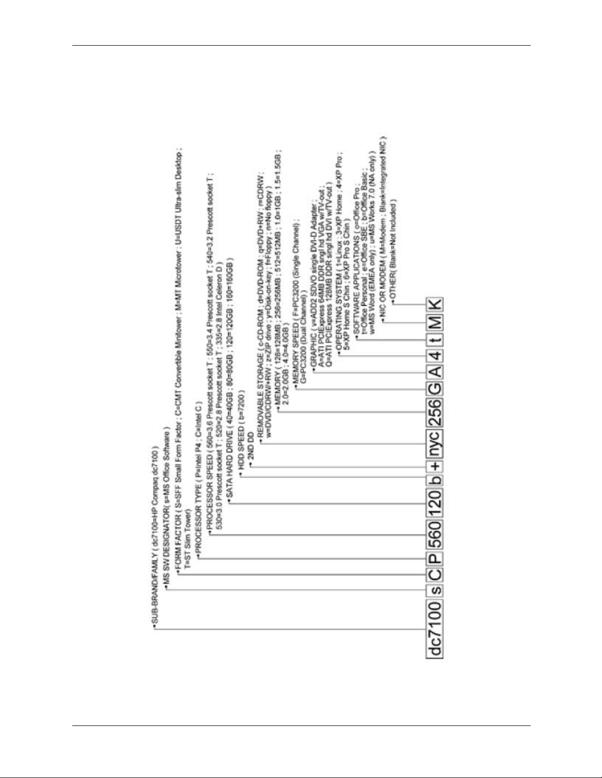
1.3 Model Numbering Convention
The model numbering convention or HP systems is as follows:
1-2 361834-002 Technical Reference Guide
Page 9

1.4 Serial Number
The unit's serial number is located on a sticker placed on the exterior cabinet. The serial number
is also written into firmware and may be read with HP Diagnostics or Insight Manager utilities.
1.5 Notational Conventions
The notational guidelines used in this guide are described in the following subsections.
1.5.1 Values
Hexadecimal values are indicated by a numerical or alpha-numerical value followed by the letter
“h.” Binary values are indicated by a value of ones and zeros followed by the letter “b.”
Numerical values that have no succeeding letter can be assumed to be decimal unless otherwise
stated.
1.5.2 Ranges
Ranges or limits for a parameter are shown using the following methods:
Example A: Bits <7..4> = bits 7, 6, 5, and 4.
Introduction
Example B: IRQ3-7, 9 = IRQ signals 3 through 7, and IRQ signal 9
1.5.3 Register Notation and Usage
This guide uses standard Intel naming conventions in discussing the microprocessor's (CPU)
internal registers. Registers that are accessed through programmable I/O using an indexing
scheme are indicated using the following format:
03C5.17h
In the example above, register 03C5.17h is accessed by writing the index port value 17h to the
index address (03C4h), followed by a write to or a read from port 03C5h.
1.5.4 Bit Notation and Byte Values
Bit designations are labeled between brackets (i.e., “bit <0 >”). Binary values are shown with the
most significant bit (MSb) on the far left, least significant bit (LSb) at the far right. Byte values in
hexadecimal are also shown with the MSB on the left, LSB on the right.
Index port
Data port
Technical Reference Guide 361834-002 1-3
Page 10

Introduction
1.6 Common Acronyms and Abbreviations
Table 1-1 lists the acronyms and abbreviations used in this guide.
Table 1-1
Acronyms and Abbreviations
Acronym or
Abbreviation Description
Aampere
AC alternating current
ACPI Advanced Configuration and Power Interface
A/D analog-to-digital
ADC Analog-to-digital converter
ADD or ADD2 Advanced digital display (card)
AGP Accelerated graphics port
API application programming interface
APIC Advanced Programmable Interrupt Controller
APM advanced power management
AOL Alert-On-LAN™
ASIC application-specific integrated circuit
ASF Alert Standard Format
AT 1. attention (modem commands) 2. 286-based PC architecture
ATA AT attachment (IDE protocol)
ATAPI ATA w/packet interface extensions
AVI audio-video interleaved
AVGA Advanced VGA
AWG American Wire Gauge (specification)
BAT Basic assurance test
BCD binary-coded decimal
BIOS basic input/output system
bis second/new revision
BNC Bayonet Neill-Concelman (connector type)
bps or b/s bits per second
BSP Bootstrap processor
BTO Built to order
CAS column address strobe
CD compact disk
CD-ROM compact disk read-only memory
CDS compact disk system
CGA color graphics adapter
1-4 361834-002 Technical Reference Guide
Page 11

Table 1-1
Acronyms and Abbreviations
Acronym or
Abbreviation Description
Ch Channel, chapter
cm centimeter
CMC cache/memory controller
CMOS complimentary metal-oxide semiconductor (configuration memory)
Cntlr controller
Cntrl control
codec 1. coder/decoder 2. compressor/decompressor
CPQ Compaq
CPU central processing unit
CRIMM Continuity (blank) RIMM
CRT cathode ray tube
CSM 1. Compaq system management 2. Compaq server management
Introduction
DAC digital-to-analog converter
DC direct current
DCH DOS compatibility hole
DDC Display Data Channel
DDR Double data rate (memory)
DIMM dual inline memory module
DIN Deutche IndustriNorm (connector type)
DIP dual inline package
DMA direct memory access
DMI Desktop management interface
dpi dots per inch
DRAM dynamic random access memory
DRQ data request
DVI Digital video interface
dword Double word (32 bits)
EDID extended display identification data
EDO extended data out (RAM type)
EEPROM electrically eraseable PROM
EGA enhanced graphics adapter
EIA Electronic Industry Association
EISA extended ISA
EPP enhanced parallel port
EIDE enhanced IDE
Technical Reference Guide 361834-002 1-5
Page 12

Introduction
Table 1-1
Acronyms and Abbreviations
Acronym or
Abbreviation Description
ESCD Extended System Configuration Data (format)
EV Environmental Variable (data)
ExCA Exchangeable Card Architecture
FIFO first in/first out
FL flag (register)
FM frequency modulation
FPM fast page mode (RAM type)
FPU Floating point unit (numeric or math coprocessor)
FPS Frames per second
ft Foot/feet
GB gigabyte
GMCH Graphics/memory controller hub
GND ground
GPIO general purpose I/O
GPOC general purpose open-collector
GART Graphics address re-mapping table
GUI graphic user interface
hhexadecimal
HW hardware
hex hexadecimal
Hz Hertz (cycles-per-second)
ICH I/O controller hub
IDE integrated drive element
IEEE Institute of Electrical and Electronic Engineers
IF interrupt flag
I/F interface
IGC integrated graphics controller
in inch
INT interrupt
I/O input/output
IPL initial program loader
IrDA Infrared Data Association
IRQ interrupt request
ISA industry standard architecture
1-6 361834-002 Technical Reference Guide
Page 13

Table 1-1
Acronyms and Abbreviations
Acronym or
Abbreviation Description
Kb/KB kilobits/kilobytes (x 1024 bits/x 1024 bytes)
Kb/s kilobits per second
kg kilogram
KHz kilohertz
kV kilovolt
lb pound
LAN local area network
LCD liquid crystal display
LED light-emitting diode
LPC Low pin count
LSI large scale integration
LSb/LSB least significant bit/least significant byte
Introduction
LUN logical unit (SCSI)
m Meter
MCH Memory controller hub
MMX multimedia extensions
MPEG Motion Picture Experts Group
ms millisecond
MSb/MSB most significant bit/most significant byte
mux multiplex
MVA motion video acceleration
MVW motion video window
n variable parameter/value
NIC network interface card/controller
NiMH nickel-metal hydride
NMI non-maskable interrupt
NRZI Non-return-to-zero inverted
ns nanosecond
NT nested task flag
NTSC National Television Standards Committee
NVRAM non-volatile random access memory
OS operating system
PAL 1. programmable array logic 2. phase alternating line
PATA Parallel ATA
Technical Reference Guide 361834-002 1-7
Page 14

Introduction
Table 1-1
Acronyms and Abbreviations
Acronym or
Abbreviation Description
PC Personal computer
PCA Printed circuit assembly
PCI peripheral component interconnect
PCI-E PCI Express
PCM pulse code modulation
PCMCIA Personal Computer Memory Card International Association
PEG PCI express graphics
PFC Power factor correction
PIN personal identification number
PIO Programmed I/O
PN Part number
POST power-on self test
PROM programmable read-only memory
PTR pointer
RAM random access memory
RAS row address strobe
rcvr receiver
RDRAM (Direct) Rambus DRAM
RGB red/green/blue (monitor input)
RH Relative humidity
RMS root mean square
ROM read-only memory
RPM revolutions per minute
RTC real time clock
R/W Read/Write
SATA Serial ATA
SCSI small computer system interface
SDR Singles data rate (memory)
SDRAM Synchronous Dynamic RAM
SDVO Serial digital video output
SEC Single Edge-Connector
SECAM sequential colour avec memoire (sequential color with memory)
SF sign flag
SGRAM Synchronous Graphics RAM
1-8 361834-002 Technical Reference Guide
Page 15

Table 1-1
Acronyms and Abbreviations
Acronym or
Abbreviation Description
SIMD Single instruction multiple data
SIMM single in-line memory module
SMART Self Monitor Analysis Report Technology
SMI system management interrupt
SMM system management mode
SMRAM system management RAM
SPD serial presence detect
SPDIF Sony/Philips Digital Interface (IEC-958 specification)
SPN Spare part number
SPP standard parallel port
SRAM static RAM
SSE Streaming SIMD extensions
Introduction
STN super twist pneumatic
SVGA super VGA
SW software
TAD telephone answering device
TAFI Temperature-sensing And Fan control Integrated circuit
TCP tape carrier package
TF trap flag
TFT thin-film transistor
TIA Telecommunications Information Administration
TPE twisted pair ethernet
TPI track per inch
TTL transistor-transistor logic
TV television
TX transmit
UART universal asynchronous receiver/transmitter
UDMA Ultra DMA
URL Uniform resource locator
us/µs microsecond
USB Universal Serial Bus
UTP unshielded twisted pair
Vvolt
VAC Volts alternating current
Technical Reference Guide 361834-002 1-9
Page 16

Introduction
Table 1-1
Acronyms and Abbreviations
Acronym or
Abbreviation Description
VDC Volts direct current
VESA Video Electronic Standards Association
VGA video graphics adapter
VLSI very large scale integration
VRAM Video RAM
Wwatt
WOL Wake - On-LAN
WRAM Windows RAM
ZF zero flag
ZIF zero insertion force (socket)
1-10 361834-002 Technical Reference Guide
Page 17
2.1 Introduction
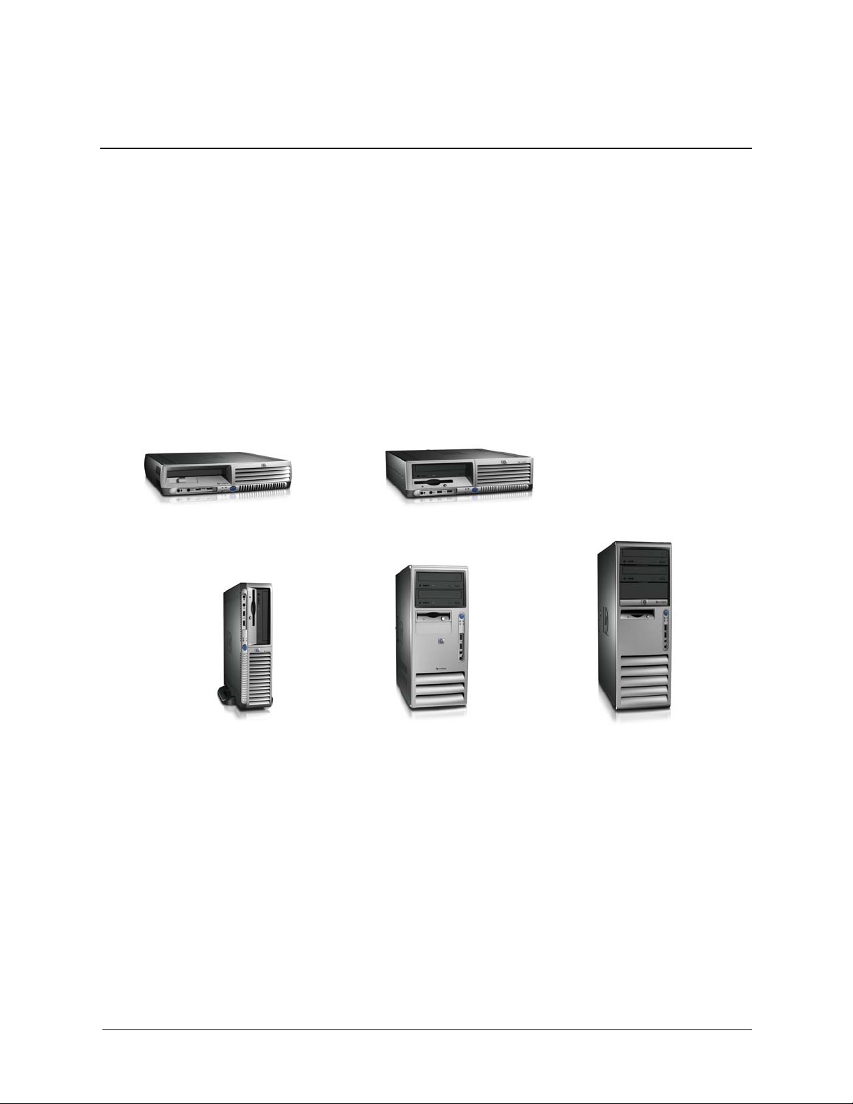
The HP Compaq dc71xx and dx61xx Series Business Desktop Computers (Figure 2-1) deliver an
outstanding combination of manageability, serviceability, and compatibility for enterprise
environments. Based on the Intel Pentium 4 processor with the Intel 915G Chipset, these systems
emphasize performance along with industry compatibility. These models feature architectures
incorporating the PCI bus. All models are easily upgradeable and expandable to keep pace with
the needs of the office enterprise.
2
System Overview
HP Compaq dc7100 USDT
HP Compaq dx61xx ST HP Compaq dx61xx MT
Figure 2-1. HP Compaq dx61xx and dc71xx Series Business Desktop Computers
This chapter includes the following topics:
■ Features (2.2), page 2-2
■ Mechanical design (2.3), page 2-4
■ System architecture (2.4), page 2-22
■ Specifications (2.5), page 2-29
HP Compaq dc7100 SFF
HP Compaq dc7100 CMT
Technical Reference Guide 361834-002 2-1
Page 18

System Overview
2.2 Features And Options
This section describes the standard features.
2.2.1 Standard Features
The following standard features are included on all series inless otherwise indicated:
■ Intel Pentium 4 processor in LGA775 (Socket T) package
■ Integrated graphics controller
■ PC2700 and PC3200 DIMMs support on dx6100 and dc7100 models
■ PC2-4300 DIMM support on dx6120 models
■ IDE controller providing serial and parallel ATA support
■ Hard drive fault prediction
■ Eight USB 2.0 ports
■ Audio processor with one headphone output, one microphone input, and one line input
■ Network interface controller providing 10/100/1000Base T support
■ Plug 'n Play compatible (with ESCD support)
■ Intelligent Manageability support
■ Energy Star compliant
■ Security features including:
❏ Flash ROM Boot Block
❏ Diskette drive disable, boot disable, write protect
❏ Power-on password
❏ Administrator password
❏ Serial/parallel port disable
■ PS/2 enhanced keyboard
■ PS/2 scroll mouse
2-2 361834-002 Technical Reference Guide
Page 19

System Overview
Table 2-1 shows the differences in features between the different PC series based on form factor:
Table 2-1
Difference Matrix by Form Factor
USDT SFF ST MT CMT
Series dc7100 dc7100 dx6100 / dx6120 dx6100 / dx6120 dc7100
System Board Type custom custom custom µATX µATX
Serial and parallel ports Optional [1] Standard Standard Standard Standard
Memory:
# of sockets
Maximum memory
Memory type
Drive bays:
Externally accessible
Internal
PCI Express slots:
x16 graphics
x1
PCI 2.3 slots 1full-height 2 half-height
MultiBay Standard Optional [7] Optional [7] not supported Optional [7]
Smart Cover Sensor / Lock Sensor only Both No No Both
Power Supply:
Power ra ting
PFC
Auto-ranging
NOTE:
[1] Supported on system board. Requires optional cable/bracket assembly.
[2] Accepts low-profile, reversed-layout ADD2/SDVO card: height = 2.5 in., length = 6.6 in.
[3] Slot not accessible in configuration using PCI riser card.
[4] Accepts standard height, normal (non-reversed) layout ADD2/SDVO card: height = 4.2 in., length = 10.5 in.
[5] Riser card configuration is a field option. Full-height PCI slots provided with configuration using PCI riser card.
Half-height dimensions: height = 2.5 in., length = 6.6 in.
Full-hieght dimensions: height = 4.2 in., length = 6.875 in
[6] PCI expansion board required for 4-slot support.
Full-height dimensions:
[7] Requires adapter.
[8] Some MT SKUs shipped with 340-watt power supplies.
3
3 GB
DDR
1
1
0
0
200-watt
Active PFC
Yes
4
4 GB
DDR
2
1
1 [2] [3]
1 [3]
or
2 full-height [5]
240 -wat t
Active PFC
Yes
4
4 GB
DDR / DDR2
2
1
1 [2] [3]
1 [3]
2 half-height
or
2 full-height [5]
240-wat t
Active PFC
Yes
4
4 GB
DDR / DDR2
3
2
1 [4]
1
2 full-height 2 full-height
300-watt [8]
Passive PF C
No
4
4 GB
DDR
4
2
1 [4]
1
or
4 full-height [6]
340-watt
Active PFC
Yes
Technical Reference Guide 361834-002 2-3
Page 20

System Overview
2.3 Mechanical Design
This guide covers six form factors:
■ Ultra Slim Desktop (USDT)—Very slim design that can be used in a tradition desktop
(horizontal) orientation or as a small tower mounted in the supplied tower stand.
■ Small Form Factor (SFF)—A small-footprint desktop requiring minimal desk space.
■ Slim Tower (ST)—Slim design that can be used in a tradition desktop (horizontal)
orientation or as a small tower mounted in the supplied tower stand.
■ Microtower (MT)- A low-height tower that requires less vertical space than a minitower.
■ Convertible Minitower (CMT) —an ATX-type unit providing the most expandability and
being adaptable to desktop (horizontal) or floor-standing (vertical) placement.
The following subsections describe the mechanical (physical) aspects of models.
CAUTION: Voltages are present within the system unit whenever the unit is plugged into a live AC outlet,
Ä
regardless of the system's “Power On” condition. Always disconnect the power cable from the power
outlet and/or from the system unit before handling the system unit in any way.
The following information is intended primarily for identification purposes only. Before servicing these systems,
refer to the applicable Service Reference Guide. Service personnel should review training materials also
✎
available on these products.
2-4 361834-002 Technical Reference Guide
Page 21
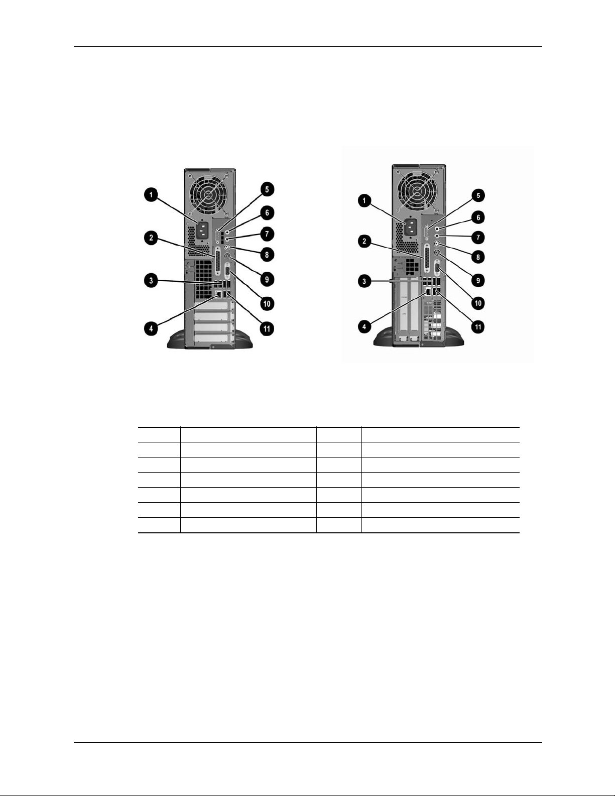
2.3.1 Cabinet Layouts
Front Views
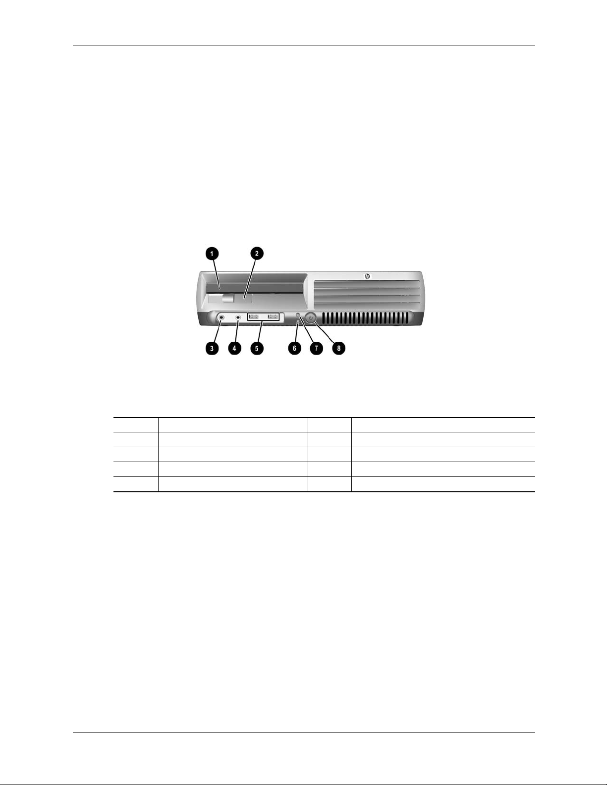
Figure 2-2 shows the front panel components of the Ultra Slim Desktop (USDT) format factor.
System Overview
Item Description Item Decription
1 MultiBay device bay 5 USB ports 7, 8
2 MultiBay device eject lever 6 Power LED
3 Microphone audio In jack 7 MultiBay device / HD activity LED
4 Headphone audio Out jack 8 Power button
Figure 2-2. HP Compaq dc7100 USDT Front View
Technical Reference Guide 361834-002 2-5
Page 22
System Overview
Figure 2-3 shows the front panel components of the Small Form Factor (SFF).
Item Description Item Decription
1 Diskette drive activity LED 7 Microphone audio In jack
2 Diskette drive media door 8 Headphone audio Out jack
3 CD-ROM drive acitvity LED 9 USB ports 7, 8
4 Diskette drive eject button 10 Hard drive activity LED
5 CD-ROM media tray 11 Power LED
6 CD-ROM drive open/close button 12 Power button
Figure 2-3. HP Compaq dc7100 SFF Front View
2-6 361834-002 Technical Reference Guide
Page 23
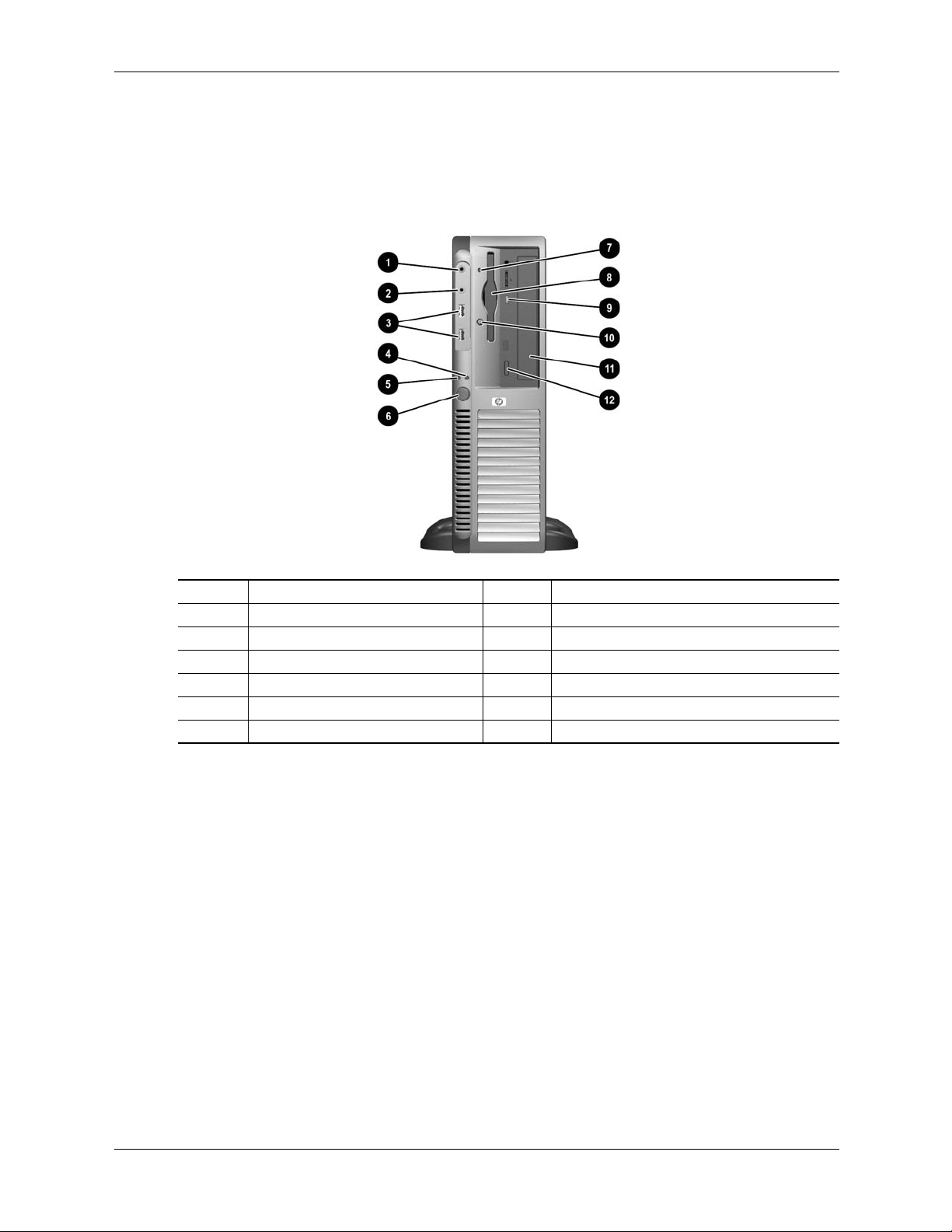
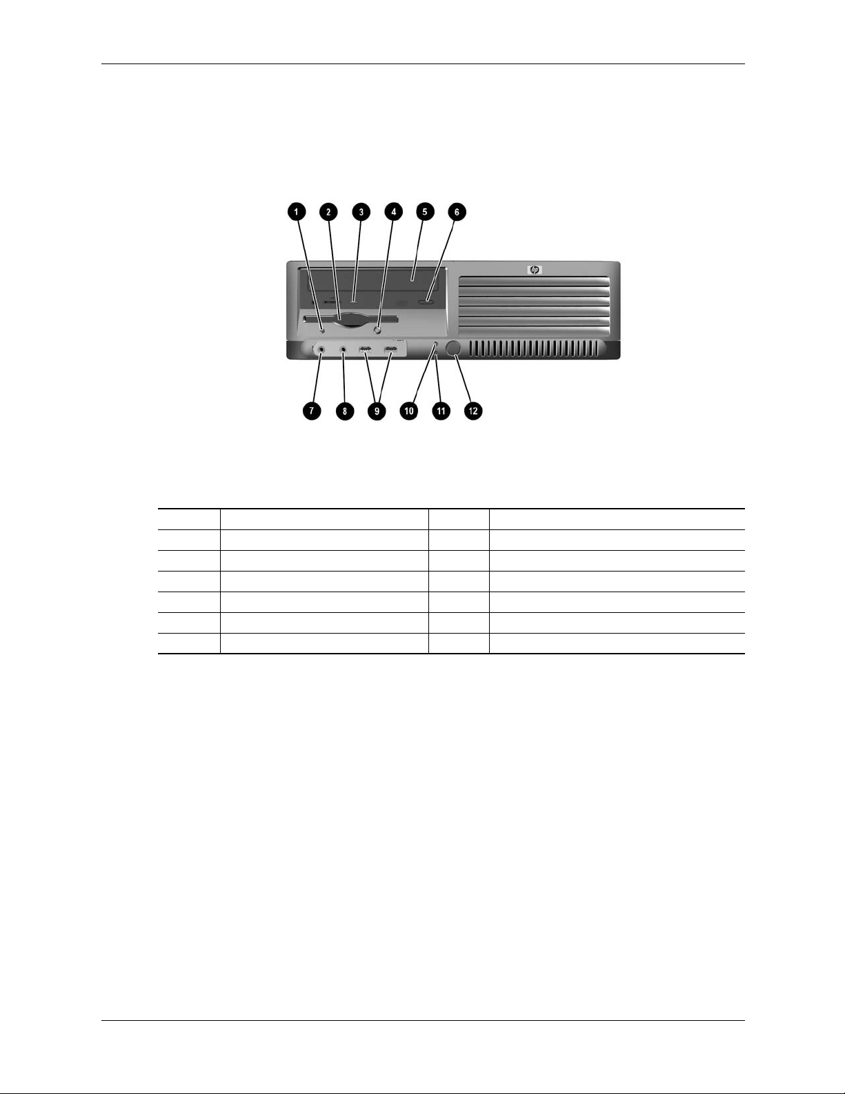
Figure 2-4 shows the front panel components of the Slim Tower (ST) form factor.
System Overview
Item Description Item Decription
1 Micorphone audio In jack 7 Diskette drive activity LED
2 Headphone audio Out jack 8 Diskette media door
3 USB ports 7, 8 9 CD-ROM drive acitvity LED
4 hard drive activity LED 10 Diskette drive eject button
5 Power LED 11 CD-ROM media tray
6 Power button 12 CD-ROM drive open/close button
Figure 2-4. HP Compaq dx6100 ST Front View
Technical Reference Guide 361834-002 2-7
Page 24

System Overview
Figure 2-5 shows the front panel components of the microtower (uT) form factor.
Item Description Item Decription
1 CD-ROM drive 7 CD-ROM drive open/close button
2 CD-ROM drive activity LED 8 Power button
3 Diskette drive media door 9 Power LED
4 Diskette drive activity LED 10 Hard drive activity LED
5 Diskette drive eject button 11 Headphone audio Out jack
6 USB ports 7, 8 12 Microphone audio In jack
Figure 2-5. HP Compaq dx6100 MT Front View
2-8 361834-002 Technical Reference Guide
Page 25
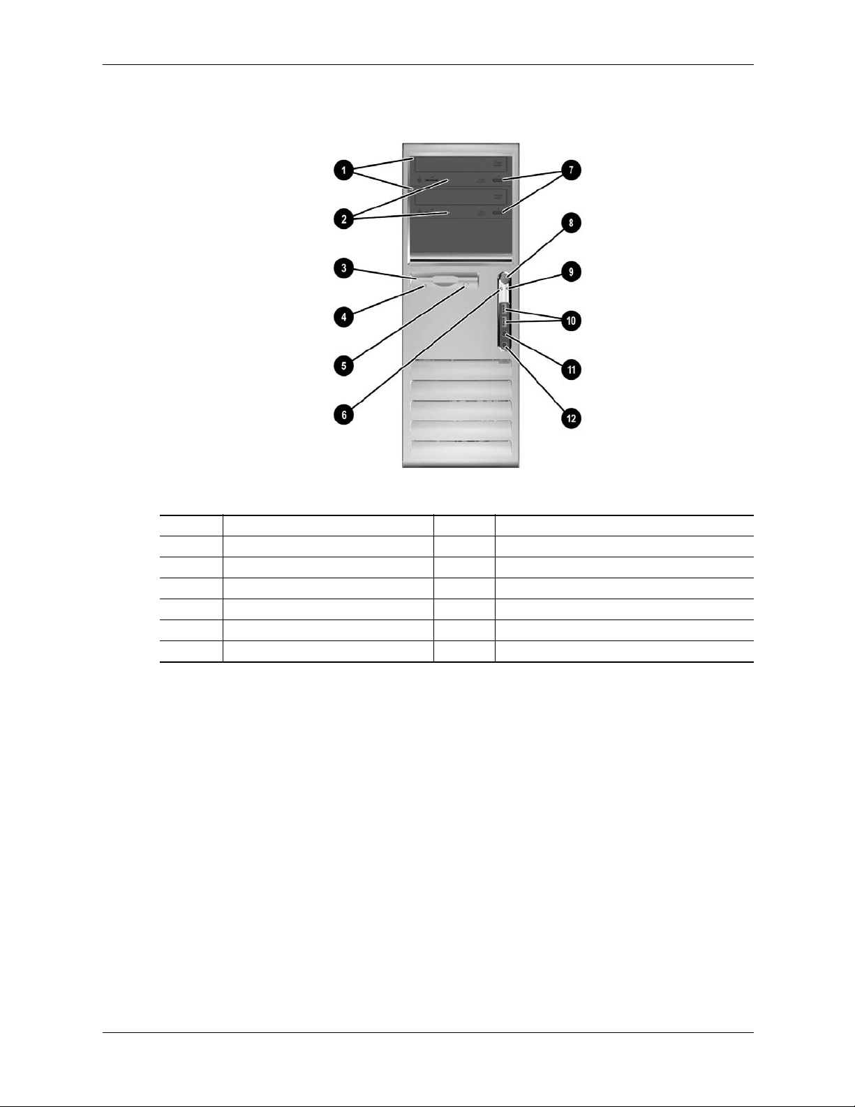
System Overview
Figure 2-6 shows the front panel components of the Convertable Minitower (CMT) form factor.
Item Description Item Decription
1 CD-ROM drive 7 CD-ROM drive open/close button
2 CD-ROM drive activity LED 8 Power button
3 Diskette drive media door 9 Power LED
4 Diskette drive activity LED 10 USB ports 7, 8
5 Diskette drive eject button 11 Headphone audio Out jack
6 Hard drive activity LED 12 Microphone audio In jack
Figure 2-6. HP Compaq dc7100 CMT Front View
Technical Reference Guide 361834-002 2-9
Page 26
System Overview
Rear Views
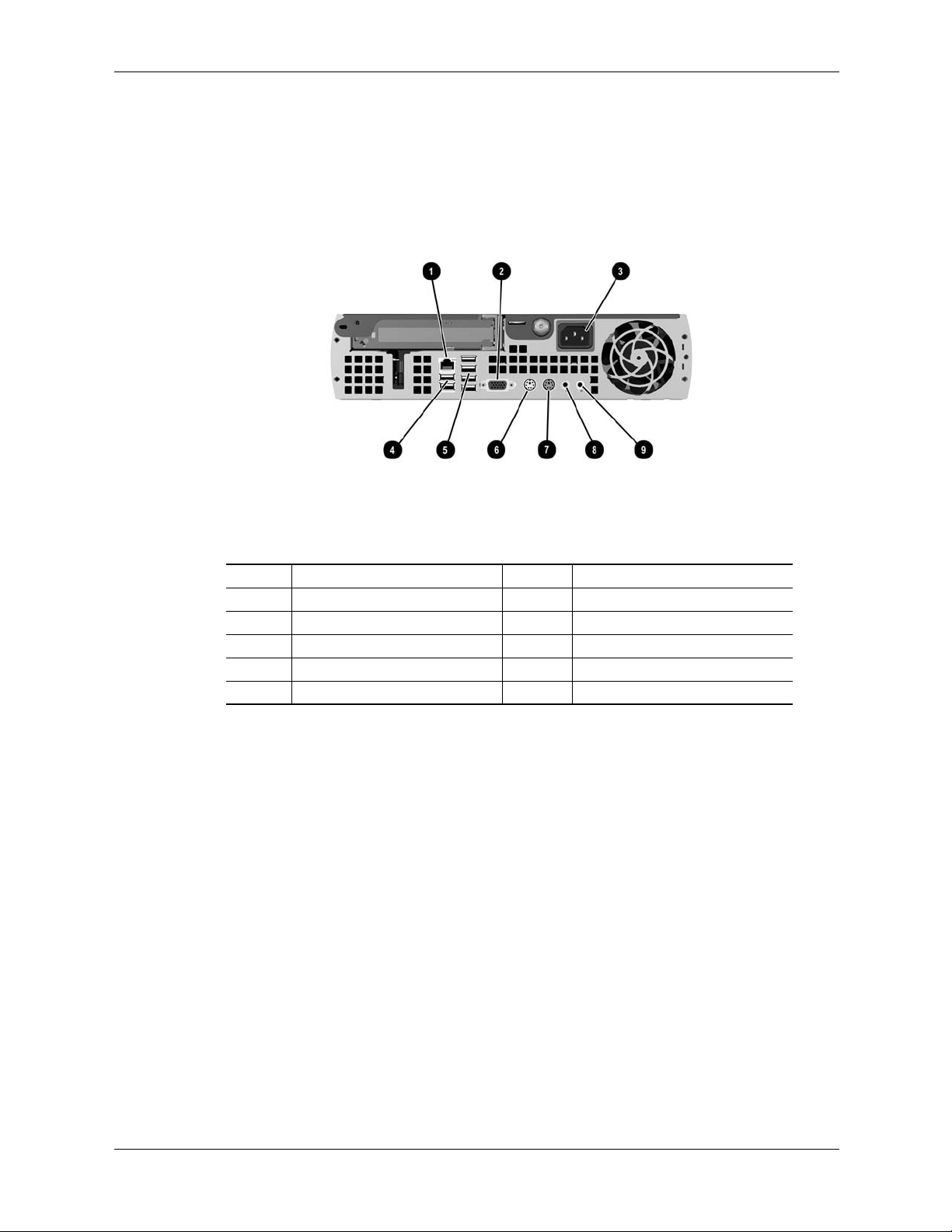
Figure 2-7 shows the rear view of the USDT form factor.
Item Description Item Description
1 NIC (LAN) connector (RJ-45) 6 Mouse connector (PS/2)
2 VGA monitor connector (DB-15) 7 Keyboard connector (PS/2)
3 AC input connector 8 Line audio In
4 USB ports 1, 2 9 Headphone / Speaker audio Out
5USB ports 3 - 6 -- --
Figure 2-7. HP Compaq dc7100 USDT, Rear View
2-10 361834-002 Technical Reference Guide
Page 27
System Overview
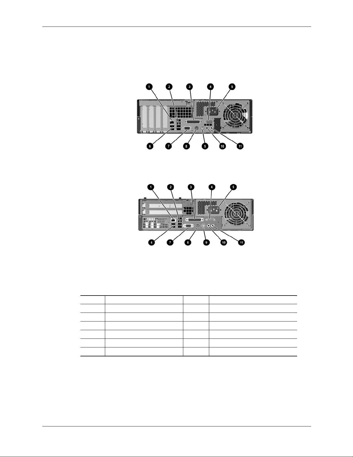
Figure 2-8 shows the rear views of the SFF form factor. Two configurations are available:
■ Without cardcage - Accepts two half-height PCI 2.3 cards, two half-height PCI Express cards
■ With card cage - Accepts two full-height PCI 2.3 cards only
SFF chassis without card cage
SFF Chassis with card cage
Item Description Item Description
1 NIC (LAN) connector (RJ-45) 7 VGA monitor connector (DB-15)
2 USB ports 3 - 6 8 Mouse connector (PS/2)
3 Parallel port (DB-25) 9 Keyboard connector (PS/2)
4 Serial port (DB-9) 10 Line audio In
5 AC input connector 11 Headphone / Speaker audio Out
6USB ports 1, 2 -- --
Figure 2-8. HP Compaq dc7100 SFF, Rear Views
Technical Reference Guide 361834-002 2-11
Page 28
System Overview
Figure 2-9 shows the rear views of the ST form factor. Two configurations are available:
■ Without cardcage - Accepts two half-height PCI 2.3 cards, two half-height PCI Express cards
■ With card cage - Accepts two full-height PCI 2.3 cards only
ST chassis without card cage
Item Description Item Description
1 AC input connector 7 Line audio In
2 Parallel port (DB-25) 8 Keyboard connector (PS/2)
3 USB ports 3 - 6 9 Mouse connector (PS/2)
4 NIC (LAN) connector (RJ-45) 10 VGA monitor connector (DB-15)
5 Serial port (DB-9) 11 USB ports 1, 2
6 Headphone / Speaker audio Out -- --
ST chassis with card cage
Figure 2-9. HP Compaq dc7100 ST, Rear Views
2-12 361834-002 Technical Reference Guide
Page 29
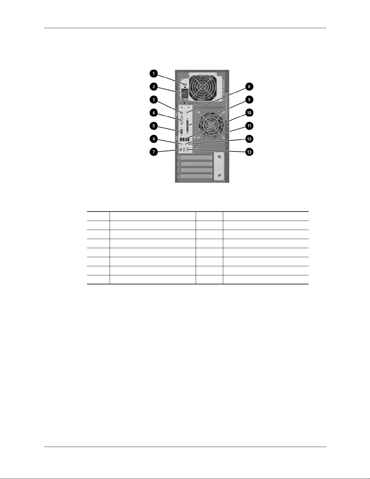
Figure 2-10 shows the rear view of the MT form factor.
System Overview
Item Description Item Description
1 AC voltage select switch [1] 8 Mouse connector (PS/2)
2 AC line connector Microphone In jack 9 Parallel port connctor (DB-25)
3 Keyboard connector (PS/2) 10 USB ports 1 - 4
4 Serial port connector (DB-9) 11 Line audio Out jack
5 VGA monitor connector (B-15) 12 Line audio In jack
6 Microphone In jack 13 NIC (LAN) connector (RJ-45)
7USB ports 5, 6 -- --
NOTE:
[1] Switch not present on SKUs that feature auto-ranging power supply.
Figure 2-10. HP Compaq dx6100 MT, Rear View
Technical Reference Guide 361834-002 2-13
Page 30
System Overview
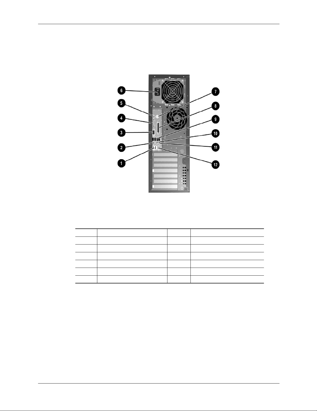
Figure 2-11 shows the rear view of the CMT form factor.
Item Description Item Description
1 USB ports 5, 6 7 Mouse connector (PS/2)
2 Microphone audio In 8 Parallel port connector (DB-25)
3 VGA monitor connector (DB-15) 9 USB ports 1-4
4 Serial port connector (DB-9) 10 Line audio Out jack
5 Keyboard connector (PS/2)) 11 Line audio In jack
6 AC line connector 12 NIC (LAN) connector (RJ-45)
Figure 2-11. HP Compaq dc7100 CMT, Rear View
2-14 361834-002 Technical Reference Guide
Page 31

2.3.2 Chassis Layouts
This section describes the internal layouts of the chassis. For detailed information on servicing
the chassis refer to the multimedia training and/or the maintenance and service guide for these
systems.
UIltra Slim Desktop Chassis
The Ultra Slim Desktop (USDT) chassis used for the HP Compaq dc7100 models uses a
compact, space-saving form factor.
System Overview
1
2
3
7
6
Item Description Item Description
1 Power supply assembly 5 Chassis fan
2 DIMM sockets (3) 6 MultiBay device
3 PCI card cage 7 Hard drive
4 Processor socket -- --
5
4
Figure 2-12. USDT Chassis Layout, TopView
Technical Reference Guide 361834-002 2-15
Page 32

System Overview
Small Form Factor / Slim Tower Chassis
The chassis layouts for the Small Form Factor (SFF) used for the HP Compaq dc7100 models
and the Slim Tower (ST) used for the HP Comapq dx6100 models are shown in Figure 2-13.
Features include:
■ Tilting drive cage assembly for easy access to processor and memory sockets
■ Two configurations:
❏ Without card cage:
◆ Two half-height, full length PCI 2.3 slots
◆ One PCI Express x16 graphics/SDVO slot
◆ One PCI Express x1 slot
❏ With card cage:
◆ Two full-height, full-length PCI 2.3 slots
-
2
9
3
4
8
5
7
1
Chassis without card cage
Item Description Item Description
1 Power supply assembly 6 Card cage
2 DIMM sockets (4) 7 Processor socket
3 PCI Express x1 slot 8 Chassis fan
4 PCI Express x16 graphics/reverse-layout slot [1] 9 Diskette drive bay
5 PCI 2.3 slots (2) 10 CD-ROM drive bay
1
Chassis with card cage
-
2
9
6
8
7
NOTE:
[1] Accepts PCI-E graphics or reversed-layout ADD2 card.
Figure 2-13. SFF / ST Chassis Layout, Top / Right Side Views
2-16 361834-002 Technical Reference Guide
Page 33

System Overview
Microtower Chassis
Figure 2-14 shows the layout for the Microtower (MT) chassis used for the HP Compaq dx6100
models. Features include:
■ Externally accessible drive bay assembly.
■ Easy access to expansion slots and all socketed system board components.
1
2
3
4
5
6
q
-
9
8
Item Description Item Description
1 Power supply assembly 7 Speaker
2 Processor socket 8 PCI 2.3 slots
3 DIMM sockets (4) 9 PCI Express x1 slot
4 DriveLock 10 PCI Express x16 graphics/normal-layout SDVO slot [1]
5 Externally accessible drive bays 11 Chassis fan
6 Internally accessible drive bays -- --
7
NOTE:
[1] Accepts PCI-E graphics or normal-layout ADD2 card.
Figure 2-14. MT Chassis Layout, Left Side View
Technical Reference Guide 361834-002 2-17
Page 34

System Overview
Convertible Minitower
Figure 2-15 shows the layout for the Convertible Minitower (CMT) chassis in the minitower
configuration used for HP Compaq dc7100 models. Features include:
■ Externally accessible drive bay assembly may be configured for minitower (vertical) or
■ Easy access to expansion slots and all socketed system board components.
desktop (horizontal) position.
w
q
-
9
8
1
2
3
4
5
6
7
Item Description Item Description
1 Power supply assembly 7 Speaker (inside card guide assembly)
2 Processor socket 8 Expansion board area
3 DIMM sockets (4) 9 PCI 2.3 slots
4 DriveLock 10 PCI Express x1 slot
5 Externally accessible drive bays 11 PCI Express x16 graphics/normal-layout SDVO slot [1]
6 Internally accessible drive bays 12 Chassis fan
NOTE:
[1] Accepts PCI-E graphics or normal-layout ADD2 card.
Figure 2-15. CMT Chassis Layout, Left Side View (Minitower configuration)
2-18 361834-002 Technical Reference Guide
Page 35

2.3.3 Board Layouts
Figures 2-16 through 2-18 show the system and expansion boards for these systems.
1
2
System Overview
3
4
5
6
o
i
u
7
8
9
y
t
-
r
e
w
q
NOTE: See USDT rear chassis illustrations for externally accessible I/O connectors.
Item Description Item Description
1 Hood sense header 11 Power button, power LED, HD LED header
2 Battery 12 Front panel audio connector
3 Parallel port option header 13 Front panel USB port connector
4 Serial port A header 14 Chassis fan, secondary connector
5 Password clear jumper header 15 Chassis fan, primary connector
6 SATA #0 header 16 DIMM sockets (3)
7 PCI 2.3 slot 17 MultiBay riser connector
8 Intenal speaker header 18 Power supply connector
9 Power supply (VccP) connector 19 Auxiliary audio input connector
10 Processor socket -- --
Figure 2-16. USDT System Board
Technical Reference Guide 361834-002 2-19
Page 36

System Overview
1
2
3
4
5
6
7
8
g
f
d
9
s
a
-
p
o
u
i
Item Description Item Description
1 Serial port B header 14 Front panel audio header
2 Battery 15 Chassis speaker connector
3 SATA #1 header 16 Front panel USB port connector
4 SATA #0 header 17 MultiBay connector
5Password jumper 18DIMM sockets (4)
6 PCI Express x1 slot 19 CD-Audio input connector
7 PCI Express x16 graphics/reversed-layout SDVO slot 20 Diskette drive connector
8 PCI 2.3 slots 21 PATA (primary IDE) connector
9 Power supply (VccP) connector 22 Auxiliary audio input connector
10 Processor socket 23 Power supply connector
11 Chassis fan, primary connector 24 Cover lock (solenoid) connector
12 Chassis fan, secondary conenctor 25 Cover sensor connector
13 Power button, power LED, HD LED header -- --
y
t
re
w
q
NOTE:
See SFF and ST rear chassis illustrations for externally accessible I/O connectors.
Figure 2-17. SFF / ST System Board
2-20 361834-002 Technical Reference Guide
Page 37

System Overview
1
1
2
3
4
5
6
7
z
l
k
j
h
g
f
d
s
p
a
o
PCI Expansion Board [1]
Item Description Item Description
1PCI 2.3 slots 16Serial ATA #2 connector [2]
2 Battery 17 Serial ATA #0 connector
3 PCI Express x1 slot 18 Hood lock header [2]
4 PCI Express x16 graphics/normal-layout SDVO slot 19 Hood sense header [2]
5 Chassis fan header 20 Password clear jumper header
6 Power supply (VccP) connector 21 Power LED/button, HD LED header
7 Serial port B header [2] 22 Serial ATA #1 connector
8 Processor socket 23 CMOS clear switch
9 Processor fan connector 24 Internal speaker connector
10 DIMM sockets (4) 25 Auxiliary audio inpout connector
11 MultiBay conector [2] 26 CD audio input connector
12 Diskette drive connector 27 Front panel USB port connector
13 Parallel ATA connector 28 PCI expansion board connector [2]
14 Power supply connector 29 Front panel audio connector
15 Serial ATA #3 connector [2] -- --
i
u
y
t
System Board
r
e
w
q
8
9
-
NOTES:
See MT and CMT rear chassis illustrations for externally accessible I/O connectors.
[1] Applicable to CMT chassis only.
[2] Not included on MT system boards.
Figure 2-18. MT / CMT System Board and CMT PCI Expansion Board
Technical Reference Guide 361834-002 2-21
Page 38

System Overview
2.4 System Architecture
The systems covered in this guide feature an architecture based on the Intel Pentium 4 processor
and the Intel 915G chipset (Figure 2-11). These systems allow processor upgrading with the Intel
Pentium 4 family and offer flexibility in expansion capabilities.
All systems covered in this guide include the following key components:
■ Intel Pentium 4 with Hyper-Threading technology, 32-KB L1 cache and 1-MB L2 cache.
■ Intel 915G/GV chipset - Includes 82915G or 82915GV GMCH north bridge and 82801
ICH6 south bridge including an integrated graphics controller, dual-channel DDR1 or DDR2
SDRAM controller, serial and parallel ATA controllers, USB 2.0 controller, and PCI
controller supporting PCI 2.3 devices.
■ SMC 47B397 super I/O controller supporting PS/2 keyboard and mouse peripherals
■ AD1981B audio controller supporting line in, speaker out, and headphone out
■ Broadcom BCM5751 10/100/1000 network interface controller
The 915G/GV chipset provides a major portion of system functionality. Designed to compliment
the latest Intel Pentium 4 processors, the chipset serves the processor through a 800-MB
Front-Side Bus (FSB). Communication between the GMCH and ICH6 components occurs
through the Direct Media Interface (DMI). The SFF, ST, MT, and CMT form factors use the
integrated graphics controller of the 82915G that may be upgraded through a PCI Express x16
graphics slot. All systems include a PCI 2.3 slot, and feature as standard a serial ATA (SATA)
hard drive with support for legacy parallel ATA 100 devices including a MultiBay device.
Table 2-2 lists the differences between models.
Table 2-2.
Architectural Differences By Form Factor
Model USDT SFF ST MT CMT
Chipset 915GV 915G 915G 915G 915G
Memory sockets 3 4 4 4 4
DDR2 models? No Yes Yes Yes Yes
Graphics upgrade PCI 2.3 card
only
PCI Express x16
graphics slot?
PCI Express x1 slot? No Yes [1] Yes [1] Yes Yes
Serial / parallel ports Optional [2] Standard [3] Standard [3] Standard [3] Standard [3]
SATA interfaces 1 2 2 4 4
Notes:
[1] Slot not accessible if PCI 2.3 full-height riser is installed.
[2] Requires adapter.
[3] 2nd serial port requires adapter.
No Yes [1] Yes [1] Yes Yes
PCI-E or
PCI 2.3 card
PCI-E or
PCI 2.3 card
PCI-E or
PCI 2.3 card
PCI-E or
PCI 2.3 card
2-22 361834-002 Technical Reference Guide
Page 39

Pentium 4
Processor
915G/GV Chipset
System Overview
Monitor
PCI Express
x16 slot (PEG)[1]
SATA
Hard Drive
MultiBay Device
CD-ROM
AC97 Audio
Subsystem
RGB
Graphics
Cntlr.
PCI Exp.
PEG I/F [1]
SATA
I/F
PATA
I/F
AC97 I/F
915 [2]
GMCH
DMI
DMI
82801
ICH6
PCI Cntlr.
PCI 2.3 slot(s)
SDRAM
Cntlr
USB
I/F
LPC I/F
Ch A DDR/DDR2
SDRAM
Ch B DDR/DDR2
SDRAM
USB Ports 1-8
Serial I/F [1]
Kybd-Mouse I/F
Keyboard
Parallel I/F [1]
LPC47B397
I/O Cntlr.
Mouse
Diskette I/F
Floppy
NIC
I/F
Note:
[1] SFF, ST, MT, and CMT form factors only.
[2] 82915GV for USDT form factor
82915G for SFF. ST. MT, and CMT form factors
PCI Express x1 slot [1]
Power Supply
Figure 2-19 System Architecture, Block diagram
Technical Reference Guide 361834-002 2-23
Page 40

System Overview
2.4.1 Intel Pentium 4 Processor
The models covered in this guide feature the Intel Pentium 4 processor with Hyper-Threading
technology. This processor is backward-compatible with software written for the Pentium III,
Pentium II, Pentium MMX, Pentium Pro, Pentium, and x86 microprocessors. The processor
architecture includes a floating-point unit, 32-KB first and 1-MB secondary caches, and
enhanced performance for multimedia applications through the use of multimedia extension
(MMX) instructions. Also included are streaming SIMD extensions (SSE and SSE2) for
enhancing 3D graphics and speech processing performance. The Pentium 4 processor features
Net-Burst Architecture that uses hyper-pipelined technology and a rapid-execution engine that
runs at twice the processor's core speed.
These systems employ a zero-insertion-force (ZIF) Socket-T designed for mounting an LGA775
processor package (Figure 2-20).
Figure 2-20. Processor Socket and Processor Package
To remove the processor:
1. Remove the processore heat sink/fan assembly (not shown).
2. Release the locking lever (1) by first pushing down, then out and up.
3. Pull up the securing frame (2).
4. Grasp the processor (3) by the edges and lift straight up from the socket.
The processor heatsink/fan assembly mounting differs between form factors. Always use the
✎
same assembly or one of the same type when replacing the processor. Refer to the applicable
Service Reference Guide for detailed removal and replacement procedures of the heatsink/fan
assembly and the processor.
2-24 361834-002 Technical Reference Guide
Page 41

2.4.2 Chipset
The chipset consists of a Graphics Memory Controller Hub (GMCH), an enhanced I/O controller
hub (ICH), and a firmware hub (FWH). Table 2-3 compares the functions provided by the
chipsets.
Components Function
82915G/GV GMCH Intel Graphics Media Accelerator 900 (integrated graphics controller)
82801EB ICH6 PCI 2.3 bus I/F
System Overview
Table 2-3
Chipset Components
PCI Express x16 graphics interface (915G only)
SDRAM controller supporting unbuffered, non-ECC PC2700/PC3200
DDR or PC2-3200/PC2-4300 DDR2 DIMMs (depending on model)
533-, or 800-MHz FSB
PCI Express x1
LPC bus I/F
SMBus I/F
IDE I/F with SATA and PATA support
AC ’97 controller
RTC/CMOS
IRQ controller
Power management logic
USB 1.1/2.0 controllers supporting eight (8) ports
82802 FWH [1] Loaded with HP/Compaq BIOS
NOTE:
[1] Or equivalent component.
Technical Reference Guide 361834-002 2-25
Page 42

System Overview
2.4.3 Support Components
Input/output functions not provided by the chipset are handled by other support components.
Some of these components also provide “housekeeping” and various other functions as well.
Table 2-4 shows the functions provided by the support components.
Support Component Functions
Component Name Function
Table 2-4
LPC47B397 I/O Controller Keyboard and pointing device I/F
BCM5751 Ethernet Controller 10/100/1000 Fast Ethernet network interface controller.
AD1981B Audio Codec Audio mixer
2.4.4 System Memory
These systems implement a dual-channel Double Data Rate (DDR) memory architecture. All
dx6100 and dc7100 models support PC2700 (333- MHz) and PC3200 (400-MHz) DIMMs. Only
dx6120 models support DDR2, PC2-4300 (533-MHz) DIMMs.
DDR and DDR2 DIMMs are NOT interchangeable. Memory type is defined by the system
✎
board.
Diskette I/F
Serial I/F (COM1and COM2)
Parallel I/F (LPT1, LPT2, or LPT3)
PCI reset generation
Interrupt (IRQ) serializer
Power button and front panel LED logic
GPIO ports
Processor over tempurature monitoring
Fan control and monitoring
Power supply voltage monitoring
SMBus and Low Pin Count (LPC) bus I/F
Digital-to-analog converter
Analog-to-digital converter
Analog I/O
6-channel audio support
The USDT system provides three DIMM sockets supporting up to 3 GB of memory while all
other form factors provide four DIMM sockets and support a total of four gigabytes of memory.
The maximum memory amounts stated above are with 1-GB memory modules using 1-Gb
✎
technology DIMMs.
2-26 361834-002 Technical Reference Guide
Page 43

2.4.5 Mass Storage
All models support at least two mass storage devices, with one being externally accessible for
removable media. These systems provide one, two, or four SATA interfaces and one PATA
interface. These systems may be preconfigured or upgraded with a 40-, 80-, or 160-GB SATA
hard drive and one removable media drive such as a CD-ROM drive. Some systems also provide
one MultiBay interface.
2.4.6 Serial and Parallel Interfaces
All models except those that use the USDT form factor include a serial port and a parallel port,
both of which are accessible at the rear of the chassis. The USDT form factor may be upgraded
with an adapter to provide serial and parallel ports. The SFF, ST, MT, and CMT form factors may
be upgraded with an optional second serial port.
The serial interface is RS-232-C/16550-compatible and supports standard baud rates up to
115,200 as well as two high-speed baud rates of 230K and 460K. The parallel interface is
Enhanced Parallel Port (EPP1.9) and Enhanced Capability Port (ECP) compatible, and supports
bi-directional data transfers.
2.4.7 Universal Serial Bus Interface
System Overview
All models provide eight Universal Serial Bus (USB) ports, with two ports accessible at the front
of the unit and six ports accessible on the rear panel. The USB interface provides hot
plugging/unplugging functionality. These systems support USB 1.1 and 2.0 functionality on all
ports.
2.4.8 Network Interface Controller
All models feature a Broadcom NetXtreme Gigabit Network Interface Controller (NIC)
integrated on the system board. The controller provides automatic selection of 10BASE-T,
100BASE-TX, or 1000BASE-T operation with a local area network and includes power-down,
wake-up, and Alert-On-LAN (AOL), and Alert Standard Format (ASF) features. An RJ-45
connector with status LEDs is provided on the rear panel.
Technical Reference Guide 361834-002 2-27
Page 44

System Overview
2.4.9 Graphics Subsystem
These systems use the 82915G or 82915GV GMCH component that integrates an Intel graphics
controller that can drive an external VGA monitor. The integrated graphics controller (IGC)
features a 333-MHz core processor and a 400-MHz RAMDAC. The controller implements
Dynamic Video Memory Technology (DVMT 3.0) for video memory. Table 2-5 lists the key
features of the integrated graphics subsystem.
Integrated Graphics Subsystem Statistics
Recommended for: Hi 2D, Entry 3D
Bus Type Int. PCI Express
Memory Amount 8 MB pre-allocated
Memory Type DVMT 3.0
DAC Speed 400 MHz
Table 2-5
82915G or GV GMCH
Integrated Graphics Controller
Maximum 2D Res. 2048x1536 @ 85 Hz
Software Compatibility Quick Draw,
Outputs 1 RGB
The IGC of the 82915G used in the SFF, ST, MT, and CMT form factors supports upgrading
through a PCI Express x16 graphics slot. The IGC of the 82915GV used in the USDT form
factor does not support a PCI Express x16 graphic slot and may only be upgraded through the
PCI 2.3 slot.
2.4.10 Audio Subsystem
These systems use the integrated AC97 audio controller of the chipset and the ADI 1981B audio
codec. These systems include microphone and line inputs and headphone and line outputs and
include a 3-watt output amplifier driving an internal speaker. All models feature front
panel-accessible microphone in and headphone out audio jacks as standard.
DirectX 9.0,
Direct Draw,
Direct Show,
Open GL 1.4,
MPEG 1-2,
Indeo
2-28 361834-002 Technical Reference Guide
Page 45

2.5 Specifications
This section includes the environmental, electrical, and physical specifications for the systems
covered in this guide. Where provided, metric statistics are given in parenthesis. Specifications
are subject to change without notice.
Environmental Specifications (Factory Configuration)
Parameter Operating Non-operating
System Overview
Table 2-6
Ambient Air Temperature 50
o
to 95o F (10o to 35o C, max.
rate of change < 10°C/Hr)
-24o to 140o F (-30o to 60o C, max.
rate of change < 20°C/Hr )
Shock (w/o damage) 5 Gs [1] 20 Gs [1]
Vibration 0.000215 G
Humidity 10-90% Rh @ 28
wet bulb temperature
2
/Hz, 10-300 Hz 0.0005 G2/Hz, 10-500 Hz
o
C max.
5-95% Rh @ 38.7o C max.
wet bulb temperature
Maximum Altitude 10,000 ft (3048 m) [2] 30,000 ft (9144 m) [2]
NOTE:
[1] Peak input acceleration during an 11 ms half-sine shock pulse.
[2] Maximum rate of change: 1500 ft/min.
Table 2-7
Electrical Specifications
Parameter U.S. International
Input Line Voltage:
Nominal:
Maximum:
100–240 VAC
90–264 VAC
100–240 VAC
90–264 VAC
Input Line Frequency Range:
Nominal:
Maximum:
50–60 Hz
47–63 H z
50–60 Hz
47–63 H z
Power Supply:
Maximum Continuous Power:
USDT
ST or SFF
MT
CMT
200 watts
240 watts
300 watts [1]
340 watts
200 watts
240 watts
300 watts [1]
340 watts
Maximum Line Current Draw:
USDT
SF or SFF
MT
CMT
NOTES:
[1] Some MT SKUs shpped with 340-watt power supplies.
4 A @ 100 VAC
5 A @ 100 VAC
8 A @ 100 VAC
6 A @ 100 VAC
2 A @ 200 VAC
2.5 A @ 200 VAC
4 A @ 200 VAC
3.0 A @ 200 VAC
Technical Reference Guide 361834-002 2-29
Page 46

System Overview
Parameter USDT ST SFF MT CMT [3]
Table 2-8
Physical Specifications
Height 2.95 in
(7.49 cm)
Width 12.4 in
(31.5 cm)
Depth 13.18 in
(33.48 cm)
Weight [1] 13.2 lb [2]
(6.0 kg) [2]
Load-bearing ability
of chassis [4]
NOTES:
[1] System weight may vary depending on installed drives/peripherals.
[2] Without MultiBay device installed.
[3] Minitower configuration. For desktop configuration, swap Height and Width dimensions.
[4] Applicable To unit in desktop orientation only and assumes reasonable type of load such
100 lb
(45.4 kg)
as a monitor.
3.95 in
(10.03 cm)
13.3 in
(33.78 cm)
14.9 in
(37.85 cm)
19.5 lb
(8.8 kg)
100 lb
(45.4 kg)
3.95 in
(10.03 cm)
13.3 in
(33.78 cm)
14.9 in
(37.85 cm)
19.5 lb
(8.8 kg)
100 lb
(45.4 kg)
14.5 in
(36.8 cm)
6.88 in
17.5 cm)
16.31 in
(41.1 cm)
23.8 lb
(10.8 kg)
n/a 100 lb
17.65 in
(44.8 cm)
6.60 in
(16.8 cm)
17.8 in
(45.21 cm)
32.5 lb
(14.7 kg)
(45.4 kg)
2-30 361834-002 Technical Reference Guide
Page 47

Table 2-9
Diskette Drive Specifications
Parameter Measurement
Media Type 3.5 in 1.44 MB/720 KB diskette
Height 1/3 bay (1 in)
Bytes per Sector 512
Sectors per Track:
High Density
Low Density
Tracks per Side:
High Density
Low Density
Read/Write Heads 2
Average Access Time:
Track-to-Track (high/low)
Average (high/low)
Settling Time
Latency Average
18
9
80
80
3 ms/6 ms
94 ms/169 ms
15 ms
100 ms
System Overview
Technical Reference Guide 361834-002 2-31
Page 48

System Overview
Parameter 48x CD-ROM 48/24/28x CD-RW Drive
Interface Type IDE IDE
Table 2-10
Optical Drive Specifications
Media Type (reading)
Media Type (writing) N/a CD-R, CD-RW
Transfer Rate (Reads) 4.8 Kb/s (max sustained) CD-ROM, 4.8 Kb/s;
Transfer Rate (Writes): N/a CD-R, 2.4 Kbps (sustained);
Capacity:
Mode 1, 12 cm
Mode 2, 12 cm
8 cm
Center Hole Diameter 15 mm 15 mm
Disc Diameter 8/12 cm 8/12 cm
Disc Thickness 1.2 mm 1.2 mm
Track Pitch 1.6 um 1.6 um
Laser
Beam Divergence
Output Power
Type
Wave Length
Mode 1,2, Mixed Mode, CD-DA,
Photo CD, Cdi, CD-XA
550 MB
640 MB
180 MB
+/- 1.5 °
0.14 mW
GaAs
790 +/- 25 nm
Mode 1,2, Mixed Mode, CD-DA,
Photo CD, Cdi, CD-XA
CD-ROM/CD-R, 1.5-6 Kb/s
CD-RW, 1.5 Kbps (sustained);
650 MB @ 12 cm
53.5 + 1.5°
53.6 0.14 mW
GaAs
790 +/- 25 nm
Average Access Time:
Random
Full Stroke
Audio Output Level 0.7 Vrms 0.7 Vrms
Cache Buffer 128 KB 128 KB
2-32 361834-002 Technical Reference Guide
<100 ms
<150 ms
<120 ms
<200 ms
Page 49

Table 2-11
Hard Drive Specifications
Parameter 40 GB 80 GB 160 GB
Drive Size 3.5 in 3.5 in 3.5 in
Interface SATA SATA SATA
Transfer Rate 150 MB/s 150 MB/s 150 MB/s
System Overview
Drive Protection System
Support?
Typical Seek Time (w/settling)
Single Track
Average
Full Stroke
Disk Format (logical blocks) 78,165,360 156,301,488 320,173,056
Rotation Speed 5400/7200 5400/7200 7200 RPM
Drive Fault Prediction SMART III SMART III SMART III
Yes Yes Yes
1.2 ms
8.0 ms
18 ms
0.8 ms
9.0 ms
17 ms
0.8 ms
9 ms
17 ms
Technical Reference Guide 361834-002 2-33
Page 50

System Overview
2-34 361834-002 Technical Reference Guide
Page 51

3.1 Introduction
This chapter describes the processor/memory subsystem. These systems feature the Intel
Pentium 4 processor and the 915G chipset (Figure 3-1). The dx6100 and dc7100 models support
PC2700 or PC3200 DDR memory and come standard with PC3200 DIMMs installed. The
dx6120 models support PC2-4300 DDR2 DIMMs only.
3
Processor/Memory Subsystem
Pentium 4
Processor
FSB I/F
82915G
GMCH
Note:
[1] SFF, ST, MT, and CMT models only.
Figure 3-1. Processor/Memory Subsystem Architecture
SDRAM
Cntrl
XMM1
Ch A
DIMM
Ch B
DIMM
XMM3
XMM2 [1]
Ch A
DIMM
Ch B
DIMM
XMM4
This chapter includes the following topics:
■ Pentium 4 processor (3.2), page 3-2
■ Memory subsystem (3.3), page 3-4
Technical Reference Guide 361834-002 3-1
Page 52

Processor/Memory Subsystem
3.2 Pentium 4 Processor
These systems each feature an Intel Pentium 4 processor in a FC-LGA775 package mounted with
a passive heat sink in a zero-insertion force socket. The mounting socket allows the processor to
be easily changed for servicing and/or upgrading.
3.2.1 Processor Overview
The Intel Pentium 4 processor represents the latest generation of Intel's IA32-class of processors.
Featuring Intel's NetBurst architecture and Hyper-Threading technology, the Pentium 4
processor is designed for intensive multimedia and internet applications of today and the future
while maintaining compatibility with software written for earlier (Pentium III, Pentium II,
Pentium, Celeron, and x86) microprocessors. Key features of the Pentium 4 processor include:
■ Hyper-Threading Technology—The main processing loop has twice the depth (20 stages) of
earlier processors allowing for increased processing frequencies.
■ Execution Trace Cache— A new feature supporting the branch prediction mechanism, the
trace cache stores translated sequences of branching micro-operations ( ops) and is checked
when suspected re-occurring branches are detected in the main processing loop. This feature
allows instruction decoding to be removed from the main processing loop.
■ Rapid Execution Engine—Arithmetic Logic Units (ALUs) run at twice (2x) processing
frequency for higher throughput and reduced latency.
■ 1-MB Advanced transfer L2 cache—Using 32-byte-wide interface at processing speed, the
large L2 cache provides a substantial increase.
■ Advanced dynamic execution—Using a larger (4K) branch target buffer and improved
prediction algorithm, branch mis-predictions are reduced by an average of 33 % over the
Pentium III.
■ Enhanced Floating Point Processor —With 128-bit integer processing and deeper pipelining
the Pentium 4's FPU provides a 2x performance boost over the Pentium III.
■ Additional Streaming SIMD extensions (SSE2)—In addition to the SSE support provided by
previous Pentium processors, the Pentium 4 processor includes an additional 144 MMX
instructions, further enhancing:
❏ Streaming video/audio processing
❏ Photo/video editing
❏ Speech recognition
❏ 3D processing
❏ Encryption processing
■ Quad-pumped Front Side Bus (FSB)—The FSB uses a 200-MHz clock for qualifying the
buses' control signals. However, address information is transferred using a 2x strobe while
data is transferred with a 4x strobe, providing a maximum data transfer rate that is four times
that of earlier processors.
3-2 361834-002 Technical Reference Guide
Page 53

Processor/Memory Subsystem
Figure 3-2 illustrates the internal architecture of the Intel Pentium 4 processor.
Pentium 4 Processor
Branch
Prediction
Rapid Exe. Eng.
ALUs
Core speed
Pentium Type Core Speed ALU Speed FSB Speed L2 Cache Size
P4 560
P4 550
P4 540
P4 530
P4 520
16-K Execution
Trace Cache
CPU
Out-of-Order
Core
ALU Speed (Core speed x2)
3.60 GHz 7. 2 G Hz 800 MHz 1 MB
3.40 GHz 6.8 GHz 800 MHz 1 MB
3.20 GHz 6.4 GHz 800 MHz 1 MB
3.00 GHz 6.0 GHz 800 MHz 1 MB
2.80 GHz 5.6 GHz 800 MHz 1 MB
128-bit
Integer
FPU
FSB
I/F
Cache
FSB speed (max. data transfer rate)
8-K
L1
Data
L2
1-MB
Adv..
L2
Transfer
Cache
Figure 3-2. Pentium 4 Processor Internal Architecture
The Intel Pentium 4 increases processing speed by using higher clock speeds with
hyper-pipelined technology, therefore handling significantly more instructions at a time. The
Pentium 4 features a branch prediction mechanism improved with the addition of an execution
trace cache and a refined prediction algorithm. The execution trace cache can store 12 kilobytes
of micro-ops (decoded instructions dealing with branching sequences) that are checked when
re-occurring branches are processed. Code that is not executed (bypassed) is no longer stored in
the L1 cache as was the case in the Pentium III.
The front side bus (FSB) of the Pentium 4 uses a 200-MHz clock but provides bi- and
quad-pumped transfers through the use of 2x- and 4x-MHz strobes. The Pentium 4 processor is
compatible with software written for x86 processors.
3.2.2 Processor Upgrading
All units use the LGA775 ZIF (Socket T) mounting socket. These systems require that the
processor use an integrated heatsink/fan assembly. A replacement processor must use the same
type heatsink/fan assembly as the original to ensure proper cooling.
The processor uses a PLGA775 package consisting of the processor die mounted “upside down”
on a PC board. This arrangement allows the heat sink to come in direct contact with the processor
die. The heat sink and attachment clip are specially designed provide maximum heat transfer
from the processor component.
CAUTION: Attachment of the heatsink to the processor is critical on these systems. Improper attachment
Ä
of the heatsink will likely result in a thermal condition. Although the system is designed to detect thermal
conditions and automatically shut down, such a condition could still result in damage to the processor
component. Refer to the applicable Service Reference Guide for processor installation instructions.
CAUTION: Installing a processor that is not supported by the system board may cause damage to the
Ä
system board and/or the processor.
Technical Reference Guide 361834-002 3-3
Page 54

Processor/Memory Subsystem
3.3 Memory Subsystem
The dx6100 and dc7100 models support PC2700 or PC3200 DDR memory and come standard
with PC3200 DIMMs installed. The dx6120 models support PC2-4300 DDR2 memory only.
The DDR SDRAM “PCxxxx” reference designates bus bandwidth (i.e., a PC2700 DIMM can,
✎
operating at a 333-MHz effective speed, provide a throughput of 2700 MBps (8 bytes ×
333MHz)). Memory speed types may be mixed within a system, although the system BIOS will
set the memory controller to work at speed of the slowest DIMM.
The system board provides three or four DIMM sockets depending on form factor:
■ XMM1 (black connector), channel A (all form factors
■ XMM2 (DDR, blue connector; DDR2, white connector), channel A (SFF, ST, MT, and CMT
form factors only)
■ XMM3 (black connector), channel B (all form factors)
■ XMM4 (DDR, blue connector; DDR2, white connector), channel B (all form factors)
DIMMs do not need to be installed in pairs although installation of pairs (an equal DIMM for
each channel) provides the best performance. The BIOS will detect the DIMM population and set
the system accordingly as follows:
■ Single-channel mode - DIMMs installed for one channel only
■ Dual-channel asymetric mode - DIMMs installed for both channels but of unequal channel
capacities.
■ Dual-channel interleaved mode (recommended)- DIMMs installed for both channels and
offering equal channel capacities, proving the highest performance.
These systems require DIMMs with the following parameters:
■ Unbuffered, compatible with SPD rev. 1.0
■ 256-Mb, 512-Mb, and 1-Gb memory technology
■ x8 and x16 DDR devices
■ CAS latency (CL) of 2.5 or 3
■ Single or double-sided
■ Non-ECC memory only
The SPD format supported by these systems complies with the JEDEC specification for 128-byte
EEPROMs. This system also provides support for 256-byte EEPROMs to include additional
HP-added features such as part number and serial number. The SPD format as supported in this
system (SPD rev. 1) is shown in Table 3-1.
If BIOS detects an unsupported DIMM, a “memory incompatible” message will be displayed
and the system will halt. These systems are shipped with non-ECC DIMMs only. Refer to
chapter 8 for a description of the BIOS procedure of interrogating DIMMs.
An installed mix of DIMM types (i.e., PC2700 and PC3200, CL 2 and CL 3) is acceptable but
operation will be constrained to the level of the DIMM with the lowest (slowest) performance
specification.
If an incompatible DIMM is detected the NUM LOCK will blink for a short period of time
during POST and an error message may or may not be displayed before the system hangs.
3-4 361834-002 Technical Reference Guide
Page 55

Processor/Memory Subsystem
Table 3-1 shows suggested memory configurations for these systems.
NOTE: Table 3-1 does not list all possible configurations. Balanced-capacity, dual-channel
loading yields best performance.
Table 3-1.
DIMM Socket Loading
Channel A Channel B
Socket 1 Socket 2 [1] Socket 3 Socket 4 Total
128-MB none none none 128-MB
128-MB none 128-MB none 256-MB (dual-channel)
128-MB 128-MB 128-MB none 384-MB (dual-channel)
128-MB 128-MB 128-MB 128-MB 512-MB (dua- channel)
256-MB none none none 256-MB
256-MB none 256-MB none 512-MB (dual-channel)
512-MB none none none 512-MB
512-MB none 512-MB none 1-GB (dual-channel)
1-GB none none none 1-GB
1-GB none 1-GB none 2-GB (dual-channel)
1-GB 1-GB 1-GB none 3-GB (dual-channel)
1-GB 1-GB 1-GB 1-GB 4-GB (dual-channel)
NOTE:
[1] SFF, ST, MT, and CMT form factors only.
DDR and DDR2 DIMMs are NOT interchangeable. Memory type is defined by the system
✎
board.
Technical Reference Guide 361834-002 3-5
Page 56

Processor/Memory Subsystem
The SPD address map is shown in Table 3-2.
Byte Description Notes Byte Description Notes
0 No. of Bytes Written Into EEPROM [1] 25 Min. CLK Cycle Time at CL X-2 [7]
1 Total Bytes (#) In EEPROM [2] 26 Max. Acc. Time From CLK @ CL X-2 [7]
2 Memory Type 27 Min. Row Prechge. Time [7]
3 No. of Row Addresses On DIMM [3] 28 Min. Row Active to Delay [7]
4 No. of Column Addresses On DIMM 29 Min. RAS to CAS Delay [7]
5 No. of Module Banks On DIMM 30-31 Reserved
6, 7 Data Width of Module 32-61 Superset Data [7]
8 Voltage Interface Standard of DIMM 62 SPD Revision [7]
9 Cycletime @ Max CAS Latency (CL) [4] 63 Checksum Bytes 0-62
10 Access From Clock [4] 64-71 JEP-106E ID Code [8]
11 Config. Type (Parity, Nonparity...) 72 DIMM OEM Location [8]
12 Refresh Rate/Type [4][5] 73-90 OEM’s Part Number [8]
13 Width, Primary DRAM 91-92 OEM’s Rev. Code [8]
14 Error Checking Data Width 93-94 Manufacture Date [8]
15 Min. Clock Delay [6] 95-98 OEM’s Assembly S/N [8]
16 Burst Lengths Supported 99-
17 No. of Banks For Each Mem. Device [4] 126 Intel frequency check
18 CAS Latencies Supported [4] 127 Reserved
19 CS# Latency [4] 128 - 131 Compaq header “CPQ1” [9]
20 Write Latency [4] 132 Header checksum [9]
21 DIMM Attributes 133 - 145 Unit serial number [9][10]
22 Memory Device Attributes 146 DIMM ID [9][11]
23 Min. CLK Cycle Time at CL X-1 [7] 147 Checksum [9]
24 Max. Acc. Time From CLK @ CL X-1 [7] 148 Reserved [9]
Table 3-2
SPD Address Map (SDRAM DIMM)
125
OEM Specific Data [8]
NOTES:
[1] Programmed as 128 bytes by the DIMM OEM
[2] Must be programmed to 256 bytes.
[3] High order bit defines redundant addressing: if set (1), highest order RAS# address must be re-sent as highest order CAS#
address.
[4] Refer to memory manufacturer’s datasheet
[5] MSb is Self Refresh flag. If set (1), assembly supports self refresh.
[6] Back-to-back random column addresses.
[7] Field format proposed to JEDEC but not defined as standard at publication time.
[8] Field specified as optional by JEDEC but required by this system.
[9] HP usage. This system requires that the DIMM EEPROM have this space available for reads/writes.
[10] Serial # in ASCII format (MSB is 133). Intended as backup identifier in case vender data is invalid.
Can also be used to indicate s/n mismatch and flag system adminstrator of possible system Tampering.
[11]Contains the socket # of the module (first module is “1”). Intended as backup identifier (refer to note [10]).
3-6 361834-002 Technical Reference Guide
Page 57

Figure 3-3 shows the system memory map.
Processor/Memory Subsystem
Main
Memory
Area
DOS
Compatibilty
Area
FFFF FFFFh
FFE0 0000h
F000 0000h
0100 0000h
00FF FFFFh
0010 0000h
000F FFFFh
0000 0000h
High BIOS Area
DMI/APIC
Area
PCI
Memory
Area
IGC (1-32 MB)
TSEG
Main
Memory
Main
Memory
BIOS
Extended BIOS
Expansion Area
Legacy Video
Base Memory
4 GB
Top of DRAM
16 MB
1 MB
640 KB
All locations in memory are cacheable. Base memory is always mapped to DRAM. The next 128
✎
KB fixed memory area can, through the north bridge, be mapped to DRAM or to PCI space.
Graphics RAM area is mapped to PCI or AGP locations.
Figure 3-3. System Memory Map
Technical Reference Guide 361834-002 3-7
Page 58

Processor/Memory Subsystem
3-8 361834-002 Technical Reference Guide
Page 59

4.1 Introduction
This chapter covers subjects dealing with basic system architecture and covers the following
topics:
■ PCI bus overview (4.2), page 4-1
■ System resources (4.3), page 4-11
■
Real-time clock and configuration memory (4.4
■ System management (4.5), page 4-21
■
Register map and miscellaneous functions (4.6
This chapter covers functions provided by off-the-shelf chipsets and therefore describes only
basic aspects of these functions as well as information unique to the systems covered in this
guide. For detailed information on specific components, refer to the applicable manufacturer's
documentation.
4
System Support
), page 4-19
), page 4-26
4.2 PCI Bus Overview
This section describes the PCI bus in general and highlights bus implementation in this particular
✎
system. For detailed information regarding PCI bus operation, refer to the appropriate PCI
specification or the PCI web site: www.pcisig.com.
These systems implement the following types of PCI buses:
■ PCI 2.3 - Legacy parallel interface operating at 33-MHz
■ PCI Express - High-performance interface capable of using multiple TX/RX high-speed
lanes of serial data streams
The PCI bus handles address/data transfers through the identification of devices and functions on
the bus. A device is typically defined as a component or slot that resides on the PCI bus (although
some components such as the GMCH and ICH6 are organized as multiple devices). A function is
defined as the end source or target of the bus transaction. A device may contain one or more
functions. In the standard configuration these systems use a hierarchy of three PCI buses (Figure
4-1). The PCI bus #0 is internal to the chipset components and is not physically accessible. The
Direct Media Interface (DMI) links the GMCH and ICH6 components and operates as a subset of
the PCI bus. All PCI slots and the NIC function internal to the ICH6 reside on PCI bus #2.
Technical Reference Guide 361834-002 4-1
Page 60

System Support
82915G/GV [1]
Memory
Cntlr
Function
Host-DMI Bridge
DMI Link
DMI
PCI 2.3
Bridge
Function
Notes:
[1] USDT form factor; 82915GV; SFF, ST, MT, and CMT form factors, 82915G
[2] SFF. ST, MT, and CMT form factors only.
GMCH
PCI Bus 0
PCI Exp.
Por t 1
Function
PCI 2.3 slot(s)
Integrated
Graphics
Controller
Host-PCI Exp.
Bridge
82801 ICH6
PCI Exp.
Por t 2
Function
PCI Express x1 slot [1]
PCI Bus 1
IDE
Cntlr
Function
NIC
Cntlr
RGB Monitor
PCI Express x16 graphics slot [2]
SATA
Cntlr
Function
USB I/F
Cntlr
Function
LPC
Bridge
Function
AC97
Cntlr
Function
Figure 4-1. PCI Bus Devices and Functions
4.2.1 PCI 2.3 Bus Operation
The PCI 2.3 bus consists of a 32-bit path (AD31-00 lines) that uses a multiplexed scheme for
handling both address and data transfers. A bus transaction consists of an address cycle and one
or more data cycles, with each cycle requiring a clock (PCICLK) cycle. High performance is
realized during burst modes in which a transaction with contiguous memory locations requires
that only one address cycle be conducted and subsequent data cycles are completed using
auto-incremented addressing. Four types of address cycles can take place on the PCI bus; I/O,
memory, configuration, and special. Address decoding is distributed (left up to each device on
the PCI bus).
I/O and Memory Cycles
For I/O and memory cycles, a standard 32-bit address decode (AD31..0) for byte-level
addressing is handled by the appropriate PCI device. For memory addressing, PCI devices
decode the AD31..2 lines for dword-level addressing and check the AD1,0 lines for burst
(linear-incrementing) mode. In burst mode, subsequent data phases are conducted a dword at a
time with addressing assumed to increment accordingly (four bytes at a time).
4-2 361834-002 Technical Reference Guide
Page 61

System Support
Configuration Cycles
Devices on the PCI bus must comply with PCI protocol that allows configuration of that device
by software. In this system, configuration mechanism #1 (as described in the PCI Local Bus
specification Rev. 2.3) is employed. This method uses two 32-bit registers for initiating a
configuration cycle for accessing the configuration space of a PCI device. The configuration
address register (CONFIG_ADDRESS) at 0CF8h holds a value that specifies the PCI bus, PCI
device, and specific register to be accessed. The configuration data register (CONFIG_DATA) at
0CFCh contains the configuration data.
PCI Configuration Data Register
I/O Port 0CFCh, R/W, (8-, 16-, 32-bit access)
Bit Function Bit Function
31 Configuration Enable
0 = Disabled
1 = Enable
30..24 Reserved—read/write 0s
23..16 Bus Number. Selects PCI bus
15..11 PCI Device Number. Selects PCI
device for access
10..8 Function Number. Selects function of
selected PCI device.
7..2 Register Index. Specifies config. reg.
1,0 Configuration Cycle Type ID.
00 = Type 0
01 = Type 1
PCI Configuration Address Register
I/O Port 0CF8h, R/W, (32-bit access only)
31..0 Configuration Data.
Two types of configuration cycles are used. A Type 0 (zero) cycle is targeted to a device on the
PCI bus on which the cycle is running. A Type 1 cycle is targeted to a device on a downstream
PCI bus as identified by bus number bits <23..16>. With three or more PCI buses, a PCI bridge
may convert a Type 1 to a Type 0 if it's destined for a device being serviced by that bridge or it
may forward the Type 1 cycle unmodified if it is destined for a device being serviced by a
downstream bridge. Figure 4-2 shows the configuration cycle format and how the loading of
0CF8h results in a Type 0 configuration cycle on the PCI bus. The Device Number (bits <15..11>
determines which one of the AD31..11 lines is to be asserted high for the IDSEL signal, which
acts as a “chip select” function for the PCI device to be configured. The function number (CF8h,
bits <10..8>) is used to select a particular function within a PCI component.
Register 0CF8h
Results in:
(w/Type 00
Config. Cycle)
NOTES:
32211118
Reserved
AD31..0
[1] Bits <1,0> : 00 = Type 0 Cycle, 01 = Type 1 cycle
Type 01 cycle only. Reserved on Type 00 cycle.
IDSEL (only one signal line asserted)
Bus
Number
Device
Number
Function
Number
Function
Number
7 2 1 0 [1]
Register
Register
Index
Index
Figure 4-2. Configuration Cycle
Technical Reference Guide 361834-002 4-3
Page 62

System Support
Table 4-1 shows the standard configuration of device numbers and IDSEL connections for
components and slots residing on a PCI 2.3 bus.
PCI Component Notes Function # Device #
82915G GMCH:
PCI Express x16 graphics slot [1] 0 0 32 --
82801EB ICH6
PCI 2.3 slot 1 0 4 8 AD20
Host/DMI Bridge
Host/PCI Expr. Bridge
Integrated Graphics Cntlr.
PCI Bridge
LPC Bridge
IDE Controller
Serial ATA Controller
SMBus Controller
USB I/F #1
USB I/F #2
USB I/F #3
USB I/F #4
USB 2.0 Controller
AC97 Audio Controller
AC97 Modem Controller
Network Interface Controller
PCI Express port 1
PCI Express port 2
Table 4-1
PCI Component Configuration Access
[1]
[1]
0
1
0
0
0
1
2
3
0
1
2
3
7
2
3
0
0
1
28
28
2
30
31
31
31
31
29
29
29
29
29
30
30
0
28
28
PCI Bus
#
0
0
0
0
0
0
0
0
0
0
0
0
0
0
0
64
0
0
IDSEL
Wired to:
--
--
PCI 2.3 slot 2 [2] 0 9 8 AD25
PCI 2.3 slot 3 [3] 0 10 8 AD27
PCI 2.3 slot 4 [3] 0 11 8 AD29
NOTES:
[1] Not used in these systems.
[2] SFF, ST, MT, & CMT form factors only.
[3] CMT form factor with PCI expansion board.
4-4 361834-002 Technical Reference Guide
Page 63

System Support
d
The register index (CF8h, bits <7..2>) identifies the 32-bit location within the configuration
space of the PCI device to be accessed. All PCI devices can contain up to 256 bytes of
configuration data (Figure 4-3), of which the first 64 bytes comprise the configuration space
header.
Configuration
Space
Header
31 24 23 16 15 8 7 0
Device-Specific Area
Reserved
Reserved
Expansion ROM Base Address
Subsystem Vendor IDSubsystem ID
Card Bus CIS Pointer
Base Address Registers
BIST Hdr. Type
Status
Device ID
Int. LineInt. Pin Min. GNT Min. Lat.
Line SizeLat. Timer
Command
Vendor ID
Index
FCh
40h
3Ch
38h
34h
30h
2Ch
28h
10h
0Ch
08h
04h
00h
PCI Configuration Space Type 0
Data required by PCI protocol
Figure 4-3. PCI Configuration Space Mapping
PCI 2.3 Bus Master Arbitration
Not required
31 24 23 16 15 8 7 0
Device-Specific Area
Bridge Control
Expansion ROM Base Address
Prefetchable Limit Upper 32 Bits
Prefetchable Base Upper 32 Bits
Prefetch. Mem. Limit Prefetch. Mem. Base
n
Lat.Tmr
BIST Hdr. Type
Status
Device ID
Reserved
I/O Base Upper 16 Bits
Memory BaseMemory Limit
Base Address Registers
Int. LineInt. Pin
I/O BaseI/O Limit Secondary Status
Pri. Bus #Sec. Bus # Sub. Bus # 2
Line SizeLat. Timer
Command
Vendor ID
PCI Configuration Space Type 1
Index
FCh
40h
3Ch
38h
34h
30h
2Ch
28h
24h
20h
1Ch
18h
10h
0Ch
08h
04h
00h
The PCI bus supports a bus master/target arbitration scheme. A bus master is a device that has
been granted control of the bus for the purpose of initiating a transaction. A target is a device that
is the recipient of a transaction. The Request (REQ), Grant (GNT), and FRAME signals are used
by PCI bus masters for gaining access to the PCI bus. When a PCI device needs access to the PCI
bus (and does not already own it), the PCI device asserts it's REQn signal to the PCI bus arbiter (a
function of the system controller component). If the bus is available, the arbiter asserts the GNTn
signal to the requesting device, which then asserts FRAME and conducts the address phase of the
transaction with a target. If the PCI device already owns the bus, a request is not needed and the
device can simply assert FRAME and conduct the transaction. Table 4-3 shows the grant and
request signals assignments for the devices on the PCI bus.
Technical Reference Guide 361834-002 4-5
Page 64

System Support
Device REQ/GNT Line Note
PCI Connector Slot 1 REQ0/GNT0
PCI Connector Slot 2 REQ1/GNT1 [1]
PCI Connector Slot 3 REQ2/GNT2 [2]
PCI Connector Slot 4 REQ3/GNT3 [2]
PCI bus arbitration is based on a round-robin scheme that complies with the fairness algorithm
specified by the PCI specification. The bus parking policy allows for the current PCI bus owner
(excepting the PCI/ISA bridge) to maintain ownership of the bus as long as no request is asserted
by another agent. Note that most CPU-to-DRAM and AGP-to-DRAM accesses can occur
concurrently with PCI traffic, therefore reducing the need for the Host/PCI bridge to compete for
PCI bus ownership.
Table 4-3.
PCI Bus Mastering Devices
NOTE:
[1]SFF, ST, MT, and CMT form factors only.
[2] CMT form factor with PCI expansion board
4.2.2 PCI Express Bus Operation
The PCI Express bus is a high-performace extension of the legacy PCI bus specification. The PCI
Express bus uses the following layers:
■ Software/driver layer
■ Transaction protocol layer
■ Link layer
■ Physical layer
Software/Driver Layer
The PCI Express bus maintains software compatibility with PCI 2.3 and earlier versions so that
there is no impact on existing operating systems and drivers. During system intialization, the PCI
Express bus uses the same methods of device discovery and resource allocation that legacy
PCI-based operating systems and drivers are designed to use. The use of PCI configuration space
and the programmability of I/O devices are also used in the same way as for legacy PCI buses.
The software/driver layer provides read and write requests to the transaction layer for handling a
data transfer.
Transaction Protocol Layer
The transaction protocol layer processes read and write requests from the software/driver layer
and generates request packets for the link layer. Each packet includes an identifier allowing any
required responcse packets to be directed to the originator.
PCI Express protocol supports the three legacy PCI address spaces (memory, I/O, configuration)
as well as a new message space. The message space allows in-band processing of interrupts
through use of the Message Signal Interrupt (MSI) introduced with the PCI 2.2 specification. The
MSI method eliminates the need for hard-wired sideband signals by incorporating those
functions into packets.
4-6 361834-002 Technical Reference Guide
Page 65

System Support
Link Layer
The link layer provides data integrity by adding a sequence information prefix and a CRC suffix
to the packet created by the transaction layer. Flow-control methods ensure that a packet will
only be transferred if the receiving device is ready to accomodate it. A corrupted packet will be
automatically re-sent.
Physical Layer
The PCI Express bus uses a point-to-point, high-speed TX/RX serial lane topology. that can be
scalable as to the the end point’s requirements. One or more full-duplex lanes transfer data
serially. Each lane consists of two differential pairs of signal paths (Figure 4-4), one for transmit,
one for receive.
System Board
TX
Device A
RX
PCI Express Card
Device B
Figure 4-4. PCI Express Bus Lane
Each byte is transferred using 8b/10b encoding. which embeds the clock signal with the data.
Operating at a 2.5 Gigabit transfer rate, a single lane can provide a data flow of 200 MBps. The
bandwidth is increased if additional lanes are available for use. During the initialization process,
two PCI Express devices will negotiate for the number of lanes available and the speed the link
can operate at.
In a x1 (single lane) interface, all data bytes are transferred serially over the lane. In a multi-lane
interface, data bytes are distributed across the lanes using a multiplex scheme as shown in Table
4-4:
Table 4-4.
PCI Express Byte Transfer
x1
Transfer
Byte #
00 0 0
10 1 1
20 2 2
30 3 3
40 0 4
50 1 5
60 2 6
70 3 7
Lane #
x4
Transfer
Lane #
x8
Transfer
Lane #
Technical Reference Guide 361834-002 4-7
Page 66

System Support
For a PCI Express x16 transfer, a lane will be re-used every17th byte of a transfer. The
mux-demux process provided by the physical layer is transparent to the other layers and to
software/drivers.
The SFF, ST, MT MT, and CMT forma factors provide two PCI Express slots: a PCI Express x16
(16-lane) slot specifically designed for a graphics controller, and a general purpose PCI Express
x1 (1-lane) slot.
4.2.3 Option ROM Mapping
During POST, the PCI bus is scanned for devices that contain their own specific firmware in
ROM. Such option ROM data, if detected, is loaded into system memory's DOS compatibility
area (refer to the system memory map shown in chapter 3).
4.2.4 PCI Interrupts
Eight interrupt signals (INTA- thru INTH-) are available for use by PCI devices. These signals
may be generated by on-board PCI devices or by devices installed in the PCI slots. For more
information on interrupts including PCI interrupt mapping refer to the “System Resources”
section 4.3.
4.2.5 PCI Power Management Support
This system complies with the PCI Power Management Interface Specification (rev 1.0). The
PCI Power Management Enable (PME-) signal is supported by the chipset and allows compliant
PCI peripherals to initiate the power management routine.
4-8 361834-002 Technical Reference Guide
Page 67

4.2.6 PCI Connectors
PCI 2.3 Connector
System Support
A1
B2
A49
B49
A52
B52
A62
B62
Figure 4-5. PCI 2.3 Bus Connector (32-Bit, 5.0-volt Type)
PCI 2.3 Bus Connector Pinout
Pin B Signal A Signal Pin B Signal A Signal Pin B Signal A Signal
01 -12 VDC TRST- 22 GND AD28 43 +3.3 VDC PAR
02 TCK +12 VDC 23 AD27 AD26 44 C/BE1- AD15
03 GND TMS 24 AD25 GND 45 AD14 +3.3 VDC
04 TDO TDI 25 +3.3 VDC AD24 46 GND AD13
05 +5 VDC +5 VDC 26 C/BE3- IDSEL 47 AD12 AD11
06 +5 V DC INTA- 27 AD23 +3.3 VDC 48 AD10 GN D
07 INT B- INTC - 28 G ND AD 22 49 GND AD 09
08 INTD- +5 VDC 29 AD21 AD20 50 Key Key
09 PRSNT1- Reserved 30 AD19 GND 51 Key Key
10 RSVD +5 VDC 31 +3.3 VDC AD18 52 AD08 C/BE0-
11 PRSNT2- Reserved 32 AD17 AD16 53 AD07 +3.3 VDC
12 GND GND 33 C/BE2- +3.3 VDC 54 +3.3 VDC AD06
13 GND GND 34 GND FRAME- 55 AD05 AD04
14 RSVD +3.3 AUX 35 IRDY- GND 56 AD03 GND
15 GND RST- 36 +3.3 VDC TRDY- 57 GND AD02
16 CLK +5 VDC 37 DEVSEL- GND 58 AD01 AD00
17 GND GNT- 38 GND STOP- 59 +5 VDC +5 VDC
18 REQ- GND 39 LOCK- +3.3 VDC 60 ACK64- REQ64-
19 +5 VDC PME- 40 PERR- SDONE n 61 +5 VDC +5 VDC
20 AD31 AD30 41 +3.3 VDC SBO- 62 +5 VDC +5 VDC
21 AD29 +3.3 VDC 42 SERR- GND
Table 4-5.
Technical Reference Guide 361834-002 4-9
Page 68

System Support
PCI Express Connectors
A1
A11
A12
A18
x1 Connector
x16 Connector
B1
B11
B12
Figure 4-6. PCI Express Bus Connectors
Table 4-6.
PCI Express Bus Connector Pinout
Pin B Signal A Signal Pin B Signal A Signal Pin B Signal A Signal
01 +12 VDC PRSNT1# 29 GND PERp3 57 GND PERn9
02 +12 VDC +12 VDC 30 RSVD PERn3 58 PETp10 GND
03 RSVD +12 VDC 31 PRSNT2# GND 59 PETn10 GND
04 GND GND 32 GND RSVD 60 GND PERp10
05 SMCLK +5 VDC 33 PETp4 RSVD 61 GND PERn10
06 +5 VDC JTAG2 34 PETn4 GND 62 PETp11 GND
07 GND JTAG4 35 GND PERp4 63 PETn11 GND
08 +3.3 VDC JTAG5 36 GND PERn4 64 GND PERp11
09 JTAG1 +3.3 VDC 37 PETp5 GND 65 GND PERn11
10 3.3 Vaux +3.3 VDC 38 PETn5 GND 66 PETp12 GND
11 WAKE PERST# 39 GND PERp5 67 PETn12 GND
12 RSVD GND 40 GND PERn5 68 GND PERp12
13 GND REFCLK+ 41 PETp6 GND 69 GND PERn12
14 PETp0 REFCLK- 42 PETn6 GND 70 PETp13 GND
15 PETn0 GND 43 GND PERp6 71 PETn13 GND
16 GND PERp0 44 GND PERn6 72 GND PERp13
17 PRSNT2# PERn0 45 PETp7 GND 73 GND PERn13
18 GND GND 46 PETn7 GND 74 PETp14 GND
19 PETp1 RSVD 47 GND PERp7 75 PETn14 GND
20 PETn1 GND 48 PRSNT2# PERn7 76 GND PERp14
21 GND PERp1 49 GND GND 77 GND PERn14
22 GND PERn1 50 PET p8 RSV D 78 PETp15 G ND
23 PETp2 GND 51 PETn8 GND 79 PETn15 GND
24 PETn2 GND 52 GND PERp8 80 GND PERp15
25 GND PERp2 53 GND PERn8 81 PRSNT2# PERn15
26 GND PE Rn2 54 PET p9 GND 82 RSVD GND
27 PETp3 GND 55 PETn9 GND
28 PETn3 GND 56 GND PERp9
A82
B82
4-10 361834-002 Technical Reference Guide
Page 69

4.3 System Resources
This section describes the availability and basic control of major subsystems, otherwise known as
resource allocation or simply “system resources.” System resources are provided on a priority
basis through hardware interrupts and DMA requests and grants.
4.3.1 Interrupts
The microprocessor uses two types of hardware interrupts; maskable and nonmaskable. A
maskable interrupt can be enabled or disabled within the microprocessor by the use of the STI
and CLI instructions. A nonmaskable interrupt cannot be masked off within the microprocessor,
although it may be inhibited by hardware or software means external to the microprocessor.
Maskable Interrupts
The maskable interrupt is a hardware-generated signal used by peripheral functions within the
system to get the attention of the microprocessor. Peripheral functions produce a unique INTA-H
(PCI) or IRQ0-15 (ISA) signal that is routed to interrupt processing logic that asserts the
interrupt (INTR-) input to the microprocessor. The microprocessor halts execution to determine
the source of the interrupt and then services the peripheral as appropriate.
Most IRQs are routed through the I/O controller of the super I/O component, which provides the
serializing function. A serialized interrupt stream is then routed to the ICH component.
System Support
Interrupts may be processed in one of two modes (selectable through the F10 Setup utility):
■ 8259 mode
■ APIC mode
These modes are described in the following subsections.
Technical Reference Guide 361834-002 4-11
Page 70

System Support
8259 Mode
The 8259 mode handles interrupts IRQ0-IRQ15 in the legacy (AT-system) method using
8259-equivalent logic. Table 4-7 lists the standard source configuration for maskable interrupts
and their priorities in 8259 mode. If more than one interrupt is pending, the highest priority
(lowest number) is processed first.
Table 4-7.
Maskable Interrupt Priorities and Assignments
Priority Signal Label Source (Typical)
1 IRQ0 Interval timer 1, counter 0
2 IRQ1 Keyboard
3 IRQ8- Real-time clock
4 IRQ9 Unused
5 IRQ10 PCI devices/slots
6 IRQ11 Audio codec
7 IRQ12 Mouse
8 IRQ13 Coprocessor (math)
9 IRQ14 Primary IDE controller
10 IRQ15 Sec. IDE I/F controller (not available on SATA units)
11 IRQ3 Serial port (COM2)
12 IRQ4 Serial port (COM1)
13 IRQ5 Network interface controller
14 IRQ6 Diskette drive controller
15 IRQ7 Parallel port (LPT1)
-- IRQ2 NOT AVAILABLE (Cascade from interrupt controller 2)
4-12 361834-002 Technical Reference Guide
Page 71

System Support
APIC Mode
The Advanced Programmable Interrupt Controller (APIC) mode provides enhanced interrupt
processing with the following advantages:
■ Eliminates the processor's interrupt acknowledge cycle by using a separate (APIC) bus
■ Programmable interrupt priority
■ Additional interrupts (total of 24)
The APIC mode accommodates eight PCI interrupt signals (INTA-..INTH-) for use by PCI
devices. The PCI interrupts are evenly distributed to minimize latency and wired as follows:
PCI
Slot 1
INTA-
INTB- —
INTC- INTB-
INTD- —
INTE- —
INTF- INTC-
INTG- INTD-
INTH- —
NOTES:
[1] Connection internal to the ICH. Will be reported by BIOS as using INTA but is NOT shared with
other functions using INTA.
Wired
to
MT, CMT form factors only.
SFF, ST, MT, CMT form factors only.
INTA-
PCI
Slot 2
INTD- INTB- INTD-
— — —
INTA- INTC- INTA-
— — —
— — —
INTB- INTD- INTB-
INTC- INTA- INTC-
— — —
PCI
Slot 3
PCI
Slot 4
The PCI interrupts can be configured by PCI Configuration Registers 60h..63h to share the
standard ISA interrupts (IRQn).
The APIC mode is supported by the Windows NT, Windows 2000, and Windows XP operating
✎
systems. Systems running the Windows 95 or 98 operating system will need to run in 8259 mode.
Technical Reference Guide 361834-002 4-13
Page 72

System Support
Maskable Interrupt processing is controlled and monitored through standard AT-type
I/O-mapped registers. These registers are listed in Table 4-8.
I/O Port Register
020h Base Address, Int. Cntlr. 1
021h Initialization Command Word 2-4, Int. Cntlr. 1
0A0h Base Address, Int. Cntlr. 2
0A1h Initialization Command Word 2-4, Int. Cntlr. 2
The initialization and operation of the interrupt control registers follows standard AT-type
protocol.
Non-Maskable Interrupts
Non-maskable interrupts cannot be masked (inhibited) within the microprocessor itself but may
be maskable by software using logic external to the microprocessor. There are two non-maskable
interrupt signals: the NMI- and the SMI-. These signals have service priority over all maskable
interrupts, with the SMI- having top priority over all interrupts including the NMI-.
Table 4-8.
Maskable Interrupt Control Registers
NMI- Generation
The Non-Maskable Interrupt (NMI-) signal can be generated by one of the following actions:
■ Parity errors detected on a PCI bus (activating SERR- or PERR-).
■ Microprocessor internal error (activating IERRA or IERRB)
The SERR- and PERR- signals are routed through the ICH6 component, which in turn activates
the NMI to the microprocessor.
4-14 361834-002 Technical Reference Guide
Page 73

System Support
The NMI Status Register at I/O port 061h contains NMI source and status data as follows:
NMI Status Register 61h
Bit Function
7NMI Status:
0 = No NMI from system board parity error.
1 = NMI requested, read only
6 IOCHK- NMI:
0 = No NMI from IOCHK-
1 = IOCHK- is active (low), NMI requested, read only
5 Interval Timer 1, Counter 2 (Speaker) Status
4 Refresh Indicator (toggles with every refresh)
3 IOCHK- NMI Enable/Disable:
0 = NMI from IOCHK- enabled
1 = NMI from IOCHK- disabled and cleared (R/W)
2 System Board Parity Error (PERR/SERR) NMI Enable:
0 = Parity error NMI enabled
1 = Parity error NMI disabled and cleared (R/W)
1 Speaker Data (R/W)
0 Inteval Timer 1, Counter 2 Gate Signal (R/W)
0 = Counter 2 disabled
1 = Counter 2 enabled
Functions not related to NMI activity
After the active NMI has been processed, status bits <7> or <6> are cleared by pulsing bits <2>
or <3> respectively.
The NMI Enable Register (070h, <7>) is used to enable/disable the NMI signal. Writing 80h to
this register masks generation of the NMI-. Note that the lower six bits of register at I/O port 70h
affect RTC operation and should be considered when changing NMI- generation status.
SMI- Generation
The SMI- (System Management Interrupt) is typically used for power management functions.
When power management is enabled, inactivity timers are monitored. When a timer times out,
SMI- is asserted and invokes the microprocessor's SMI handler. The SMI- handler works with the
APM BIOS to service the SMI- according to the cause of the timeout.
Although the SMI- is primarily used for power management the interrupt is also employed for
the QuickLock/QuickBlank functions as well.
Technical Reference Guide 361834-002 4-15
Page 74

System Support
4.3.2 Direct Memory Access
Direct Memory Access (DMA) is a method by which a device accesses system memory without
involving the microprocessor. Although the DMA method has been traditionally used to transfer
blocks of data to or from an ISA I/O device, PCI devices may also use DMA operation as well.
The DMA method reduces the amount of CPU interactions with memory, freeing the CPU for
other processing tasks.
This section describes DMA in general. For detailed information regarding DMA operation, refer
✎
to the data manual for the Intel 82801 I/O Controller Hub.
The 82801 ICH6 component includes the equivalent of two 8237 DMA controllers cascaded
together to provide eight DMA channels, each (excepting channel 4) configurable to a specific
device. Table 4-9 lists the default configuration of the DMA channels.
Table 4-9.
Default DMA Channel Assignments
DMA Channel Device ID
Controller 1 (byte transfers)
0
1
2
3
Controller 2 (word transfers)
4
5
6
7
Spare
Audio subsystem
Diskette drive
Parallel port
Cascade for controller 1
Spare
Spare
Spare
All channels in DMA controller 1 operate at a higher priority than those in controller 2. Note
that channel 4 is not available for use other than its cascading function for controller 1. The DMA
controller 2 can transfer words only on an even address boundary. The DMA controller and page
register define a 24-bit address that allows data transfers within the address space of the CPU.
In addition to device configuration, each channel can be configured (through PCI Configuration
Registers) for one of two modes of operation:
■ LPC DMA
■ PC/PCI DMA
The LPC DMA mode uses the LPC bus to communicate DMA channel control and is
implemented for devices using DMA through the LPC47B397 I/O controller such as the diskette
drive controller.
The PC/PCI DMA mode uses the REQ#/GNT# signals to communicate DMA channel control
and is used by PCI expansion devices.
The DMA logic is accessed through two types of I/O mapped registers; page registers and
controller registers.
4-16 361834-002 Technical Reference Guide
Page 75

System Support
DMA Page Registers
The DMA page register contains the eight most significant bits of the 24-bit address and works in
conjunction with the DMA controllers to define the complete (24-bit) address for the DMA
channels. Table 4-10 lists the page register port addresses.
Table 4-10.
DMA Page Register Addresses
DMA Channel Page Register I/O Port
Controller 1 (byte transfers)
Ch 0
Ch 1
Ch 2
Ch 3
Controller 2 (word transfers)
Ch 4
Ch 5
Ch 6
Ch 7
Refresh 08Fh [see note]
087h
083h
081h
082h
n/a
08Bh
089h
08Ah
NOTE:
The DMA memory page register for the refresh channel
must be programmed with 00h for proper operation.
The memory address is derived as follows:
24-Bit Address—Controller 1 (Byte Transfers)
8-Bit Page Register 8-Bit DMA Controller
A23..A16 A15..A00
24-Bit Address—Controller 2 (Word Transfers)
8-Bit Page Register 16-Bit DMA Controller
A23..A17 A16..A01, (A00 = 0)
Note that address line A16 from the DMA memory page register is disabled when DMA
controller 2 is selected. Address line A00 is not connected to DMA controller 2 and is always 0
when word-length transfers are selected.
By not connecting A00, the following applies:
■ The size of the the block of data that can be moved or addressed is measured in 16-bits
(words) rather than 8-bits (bytes).
■ The words must always be addressed on an even boundary.
DMA controller 1 can move up to 64 Kbytes of data per DMA transfer. DMA controller 2 can
move up to 64 Kwords (128 Kbytes) of data per DMA transfer. Word DMA operations are only
possible between 16-bit memory and 16-bit peripherals.
The RAM refresh is designed to perform a memory read cycle on each of the 512 row addresses
in the DRAM memory space. Refresh operations are used to refresh memory on the 32-bit
memory bus and the ISA bus. The refresh address is provided on lines SA00 through SA08.
Address lines LA23..17, SA18,19 are driven low.
Technical Reference Guide 361834-002 4-17
Page 76

System Support
The remaining address lines are in an undefined state during the refresh cycle. The refresh
operations are driven by a 69.799-KHz clock generated by Interval Timer 1, Counter 1. The
refresh rate is 128 refresh cycles in 2.038 ms.
DMA Controller Registers
Table 4-11 lists the DMA Controller Registers and their I/O port addresses. Note that there is a
set of registers for each DMA controller.
Table 4-11.
DMA Controller Registers
Register Controller 1 Controller 2 R/W
Status 008h 0D0h R
Command 008h 0D0h W
Mode 00Bh 0D6h W
Write Single Mask Bit 00Ah 0D4h W
Write All Mask Bits 00Fh 0DEh W
Software DRQx Request 009h 0D2h W
Base and Current Address—Ch 0 000h 0C0h W
Current Address—Ch 0 000h 0C0h R
Base and Current Word Count—Ch 0 001h 0C2h W
Current Word Count—Ch 0 001h 0C2h R
Base and Current Address—Ch 1 002h 0C4h W
Current Address—Ch 1 002h 0C4h R
Base and Current Word Count—Ch 1 003h 0C6h W
Current Word Count—Ch 1 003h 0C6h R
Base and Current Address—Ch 2 004h 0C8h W
Current Address—Ch 2 004h 0C8h R
Base and Current Word Count—Ch 2 005h 0CAh W
Current Word Count—Ch 2 005h 0CAh R
Base and Current Address—Ch 3 006h 0CCh W
Current Address—Ch 3 006h 0CCh R
Base and Current Word Count—Ch 3 007h 0CEh W
Current Word Count—Ch 3 007h 0CEh R
Temporary (Command) 00Dh 0DAh R
Reset Pointer Flip-Flop (Command) 00Ch 0D8h W
Master Reset (Command) 00Dh 0DAh W
Reset Mask Register (Command) 00Eh 0DCh W
4-18 361834-002 Technical Reference Guide
Page 77

4.4 Real-Time Clock and Configuration Memory
The Real-time clock (RTC) and configuration memory (also referred to as “CMOS”) functions
are provided by the 82801 component and is MC146818-compatible. As shown in the following
figure, the 82801 ICH6 component provides 256 bytes of battery-backed RAM divided into two
128-byte configuration memory areas. The RTC uses the first 14 bytes (00-0Dh) of the standard
memory area. All locations of the standard memory area (00-7Fh) can be directly accessed using
conventional OUT and IN assembly language instructions through I/O ports 70h/71h, although
the suggested method is to use the INT15 AX=E823h BIOS call.
System Support
0Dh
0Ch
0Bh
0Ah
09h
08h
07h
06h
05h
04h
03h
02h
01h
00h
Figure 4 11. Configuration Memory Map
A lithium 3-VDC battery is used for maintaining the RTC and configuration memory while the
system is powered down. During system operation a wire-Ored circuit allows the RTC and
configuration memory to draw power from the power supply. The battery is located in a battery
holder on the system board and has a life expectancy of four to eight years. When the battery has
expired it is replaced with a Renata CR2032 or equivalent 3-VDC lithium battery.
4.4.1 Clearing CMOS
Register D
Register C
Register B
Register A
Year
Month
Date of Month
Day of Week
Hours (Alarm)
Hours (Timer)
Minutes (Alarm)
Minutes (Timer)
Seconds (Alarm)
Seconds (Timer)
82801
Extended Config.
Memory Area
(128 bytes)
Standard Config.
Memory Area
(114 bytes)
RTC Area
(14 bytes)
FFh
80h
7Fh
0Eh
0Dh
00h
The contents of configuration memory (including the Power-On Password) can be cleared by the
following procedure:
1. Turn off the unit.
2. Disconnect the AC power cord from the outlet and/or system unit.
3. Remove the chassis hood (cover) and insure that no LEDs on the system board are
illuminated.
4. On the system board, press and hold the CMOS clear button for at least 5 seconds.
5. Replace the chassis hood (cover).
6. Reconnect the AC power cord to the outlet and/or system unit.
7. Turn the unit on.
To clear only the Power-On Password refer to section 4.5.1.
Technical Reference Guide 361834-002 4-19
Page 78

System Support
4.4.2 CMOS Archive and Restore
During the boot sequence the BIOS saves a copy of NVRAM (CMOS contents, password(s) and
other system variables) in a portion of the flash ROM. Should the system become un-usable, the
last good copy of NVRAM data can be restored with the Power Button Override function. This
function is invoked with the following procedure:
1. With the unit powered down, press and release the power button.
2. Immediately after releasing the power button in step 1, press and hold the power button until
the unit powers down. This action will be recorded as a Power Button Override event.
With the next startup sequence the BIOS will detect the occurrence of the Power Button Override
event and will load the backup copy of NVRAM from the ROM to the CMOS.
The Power Button Override feature does not allow quick cycling of the system (turning on then
✎
off). If the power cord is disconnected during the POST routine, the splash screen image may
become corrupted, requiring a re-flashing of the ROM (refer to chapter 8, BIOS ROM).
4-20 361834-002 Technical Reference Guide
Page 79

4.4.3 Standard CMOS Locations
Table 4-12 describes standard configuration memory locations 0Ah-3Fh. These locations are
accessible through using OUT/IN assembly language instructions using port 70/71h or BIOS
function INT15, AX=E823h.
Table 4-12.
Configuration Memory (CMOS) Map
Location Function Location Function
00-0Dh Real-time clock 24h System board ID
0Eh Diagnostic status 25h System architecture data
0Fh System reset code 26h Auxiliary peripheral configuration
10h Diskette drive type 27h Speed control external drive
11h Reserved 28h Expanded/base mem. size, IRQ12
12h Hard drive type 29h Miscellaneous configuration
13h Security functions 2Ah Hard drive timeout
14h Equipment installed 2Bh System inactivity timeout
15h Base memory size, low byte/KB 2Ch Monitor timeout, Num Lock Cntrl
16h Base memory size, high byte/KB 2Dh Additional flags
17h Extended memory, low byte/KB 2Eh-2Fh Checksum of locations 10h-2Dh
18h Extended memory, high byte/KB 30h-31h Total extended memory tested
19h Hard drive 1, primary controller 32h Century
1Ah Hard drive 2, primary controller 33h Miscellaneous flags set by BIOS
1Bh Hard drive 1, secondary controller 34h International language
1Ch Hard drive 2, secondary controller 35h APM status flags
1Dh Enhanced hard drive support 36h ECC POST test single bit
1Eh Reserved 37h-3Fh Power-on password
1Fh Power management functions 40-FFh Feature Control/Status
System Support
NOTES:
Assume unmarked gaps are reserved.
Higher locations (>3Fh) contain information that should be accessed using the INT15, AX=E845h
BIOS function (refer to Chapter 8 for BIOS function descriptions).
4.5 System Management
This section describes functions having to do with security, power management, temperature,
and overall status. These functions are handled by hardware and firmware (BIOS) and generally
configured through the Setup utility.
4.5.1 Security Functions
These systems include various features that provide different levels of security. Note that this
subsection describes only the hardware functionality (including that supported by Setup) and
does not describe security features that may be provided by the operating system and application
software.
Technical Reference Guide 361834-002 4-21
Page 80

System Support
Power-On / Setup Password
These systems include a power-on and setup passwords, which may be enabled or disabled
(cleared) through a jumper on the system board. The jumper controls a GPIO input to the 82801
ICH6 that is checked during POST. The password is stored in configuration memory (CMOS)
and if enabled and then forgotten by the user will require that either the password be cleared
(preferable solution and described below) or the entire CMOS be cleared (refer to section 4.4.1).
To clear the password, use the following procedure:
1. Turn off the system and disconnect the AC power cord from the outlet and/or system unit.
2. Remove the cover (hood) as described in the appropriate User Guide or Maintainance And
3. Locate the password clear jumper (header is labeled E49 on these systems) and move the
4. Replace the cover.
5. Re-connect the AC power cord to the AC outlet and/or system unit.
6. Turn on the system. The POST routine will clear and disable the password.
7. To re-enable the password feature, repeat steps 1-6, replacing the jumper on pins 1 and 2 of
Service Reference Guide. Insure that all system board LEDs are off (not illuminated).
jumper from pins 1 and 2 and place on (just) pin 2 (for safekeeping).
header E49.
Setup Password
The Setup utility may be configured to be always changeable or changeable only by entering a
password. Refer to the previous procedure (Power On / Setup Password) for clearing the Setup
password.
Cable Lock Provision
These systems include a chassis cutout (on the rear panel) for the attachment of a cable lock
mechanism.
I/O Interface Security
The serial, parallel, USB, and diskette interfaces may be disabled individually through the Setup
utility to guard against unauthorized access to a system. In addition, the ability to write to or boot
from a removable media drive (such as the diskette drive) may be enabled through the Setup
utility. The disabling of the serial, parallel, and diskette interfaces are a function of the
LPC47B397 I/O controller. The USB ports are controlled through the 82801.
Chassis Security
Some systems feature Smart Cover (hood) Sensor and Smart Cover (hood) Lock mechanisms to
inhibit unauthorized tampering of the system unit.
Smart Cover Sensor
Some systems include a plunger switch that, when the cover (hood) is removed, closes and
grounds an input of the 82801 component. The battery-backed logic will record this “intrusion”
event by setting a specific bit. This bit will remain set (even if the cover is replaced) until the
system is powered up and the user completes the boot sequence successfully, at which time the
bit will be cleared. Through Setup, the user can set this function to be used by Alert-On-LAN
and or one of three levels of support for a “cover removed” condition:
4-22 361834-002 Technical Reference Guide
Page 81

Level 0—Cover removal indication is essentially disabled at this level. During POST, status bit is
cleared and no other action is taken by BIOS.
Level 1—During POST the message “The computer's cover has been removed since the last
system start up” is displayed and time stamp in CMOS is updated.
Level 2—During POST the “The computer's cover has been removed since the last system start
up” message is displayed, time stamp in CMOS is updated, and the user is prompted for the
administrator password. (A Setup password must be enabled in order to see this option).
Smart Cover Lock (Optional)
Some systems support an optional solenoid-operated locking bar that, when activated, prevents
the cover (hood) from being removed. The GPIO ports 44 and 45 of the LPC47B397 I/O
controller provide the lock and unlock signals to the solenoid. A locked hood may be bypassed
by removing special screws that hold the locking mechanism in place. The special screws are
removed with the Smart Cover Lock Failsafe Key.
4.5.2 Power Management
This system provides baseline hardware support of ACPI- and APM-compliant firmware and
software. Key power-consuming components (processor, chipset, I/O controller, and fan) can be
placed into a reduced power mode either automatically or by user control. The system can then
be brought back up (“wake-up”) by events defined by the ACPI specification. The ACPI wake-up
events supported by this system are listed as follows:
System Support
ACPI Wake-Up Event System Wakes From
Power Button Suspend or soft-off
RTC Alarm Suspend or soft-off
Wake On LAN (w/NIC) Suspend or soft-off
PME Suspend or soft-off
Serial Port Ring Suspend or soft-off
USB Suspend only
Keyboard Suspend only
Mouse Suspend only
Technical Reference Guide 361834-002 4-23
Page 82

System Support
4.5.3 System Status
These systems provide a visual indication of system boot and ROM flash status through the
keyboard LEDs and operational status using bi-colored power and hard drive activity LEDs as
indicated in Tables 4-13 and 4-14 respectively.
The LED indications listed in Table 4-13 are valid only for PS/2-type keyboards. A USB
✎
keyboard will not provide LED status for the listed events, although audible (beep) indications
will occur.
PS/2 Keyboard System Boot/ROM Flash Status LED Indications
Event
System memory failure [1] Blinking Off Off
Graphics controller failure [2] Off Blinking Off
System failure prior to graphics cntlr. initialization [3] Off Off Blinking
ROMPAQ diskette not present, faulty, or drive prob. On Off Off
Password prompt Off On Off
Invalid ROM detected—flash failed Blinking [4] Blinking [4] Blinking [4]
Keyboard locked in network mode Blinking [5] Blinking [5] Blinking [5]
Successful boot block ROM flash On [6] On [6] On [6]
NOTES:
[1]Accompanied by 1 short, 2 long audio beeps
[2]Accompanied by 1 long, 2 short audio beeps
[3]Accompanied by 2 long, 1 short audio beeps
[4]All LEDs will blink in sync twice, accompanied by 1 long and three short audio beeps
[5]LEDs will blink in sequence (NUM Lock, then CAPs Lock, then Scroll Lock)
[6]Accompanied by rising audio tone.
Badkdd
Table 4-14 lists the audible and visible indications provided by system status conditions. .
Table 4-13.
NUM Lock
LED
CAPs Lock
LED
Scroll Lock
LED
Table 4-14.
System Operational Status LED Indications
System Status PowerLED Beeps [2] Action Required
S0: System on (normal operation) Steady green None none
S1: Suspend Blinks green @ .5 Hz None none
S3: Suspend to RAM Blinks green @ .5 Hz None none
S4: Suspend to disk Off – clear None none
S5: Soft off Off – clear None none
Processor thermal shutdown Blinks red 2 times @ I Hz [1] 2 [2] Check air flow, fans, heatsink
Processor not seated / installed Blinks red 3 times @ I Hz [1] 3 [2] Check processor presence/seating
Power supply overload failure Blinks red 4 times @ I Hz [1] 4 [2] Check voltage selector, devices, sys. bd
Memory error (pre-video) Blinks red 5 times @ I Hz [1] 5 [2] Check DIMMs, system board
Video error Blinks red 6 times @ I Hz [1] 6 [2] Check graphics card or system board
PCA failure detected by BIOS (pre-video) Blinks red 7 times @ I Hz [1] 7 [2] Replace system board
Invalid ROM checksum error Blinks red 8 times @ I Hz [1] 8 [2] Reflash BIOS ROM
Boot failure (after power on) Blinks red 9 times @ I Hz [1] 9 [2] Check power supply, processor, sys. bd
Bad option card Blinks red 10 times @ I Hz [1] 10 [2] Replace option card
[1] Repeated after 2 second pause.
[2] Beeps are produced by the on-board piezo speaker, NOT the chassis speaker.
[3] Beeps are repeated for 5 cycles, after which only blinking LED indication continues.
4-24 361834-002 Technical Reference Guide
Page 83

4.5.4 Thermal Sensing and Cooling
All systems feature a variable-speed fan mounted as part of the processor heatsink assembly. All
systems also provide or support an auxiliary chassis fan. All fans are controlled through
temperature sensing logic on the system board and/or in the power supply. There are some
electrical differences between form factors and between some models, although the overall
functionally is the same. Typical cooling conditions include the following:
1. Normal—Low fan speed.
2. Hot processor—ASIC directs Speed Control logic to increase speed of fan(s).
3. Hot power supply—Power supply increases speed of fan(s).
4. Sleep state—Fan(s) turned off. Hot processor or power supply will result in starting fan(s).
The RPM (speed) of all fans is the result of the temperature of the CPU as sensed by speed
control circuitry. The fans are controlled to run at the slowest (quietest) speed that will maintain
proper cooling.
Units using chassis and CPU fans must have both fans connected to their corresponding headers
✎
to ensure proper cooling of the system.
System Support
Technical Reference Guide 361834-002 4-25
Page 84

System Support
4.6 Register Map and Miscellaneous Functions
This section contains the system I/O map and information on general-purpose functions of the
ICH6 and I/O controller.
4.6.1 System I/O Map
Table 4-15 lists the fixed addresses of the input/output (I/O) ports.
Table 4-15
System I/O Map
I/O Port Function
0000..001Fh DMA Controller 1
0020..002Dh Interrupt Controller 1
002E, 002Fh Index, Data Ports to LPC47B397 I/O Controller (primary)
0030..003Dh Interrupt Controller
0040..0042h Timer 1
004E, 004Fh Index, Data Ports to LPC47B397 I/O Controller (secondary)
0050..0052h Timer / Counter
0060..0067h Microcontroller, NMI Controller (alternating addresses)
0070..0077h RTC Controller
0080..0091h DMA Controller
0092h Port A, Fast A20/Reset Generator
0093..009Fh DMA Controller
00A0..00B1h Interrupt Controller 2
00B2h, 00B3h APM Control/Status Ports
00B4..00BDh Interrupt Controller
00C0..00DFh DMA Controller 2
00F0h Coprocessor error register
0170..0177h IDE Controller 2 (active only if standard I/O space is enabled for primary drive)
01F0..01F7h IDE Controller 1 (active only if standard I/O space is enabled for secondary drive)
0278..027Fh Parallel Port (LPT2)
02E8..02EFh Serial Port (COM4)
02F8..02FFh Serial Port (COM2)
0370..0377h Diskette Drive Controller Secondary Address
0376h IDE Controller 2 (active only if standard I/O space is enabled for primary drive)
0378..037Fh Parallel Port (LPT1)
03B0..03DFh Graphics Controller
03BC..03BEh Parallel Port (LPT3)
03E8..03EFh Serial Port (COM3)
03F0..03F5h Diskette Drive Controller Primary Addresses
03F6h IDE Controller 1 (active only if standard I/O space is enabled for sec. drive)
03F8..03FFh Serial Port (COM1)
04D0, 04D1h Interrupt Controller
0678..067Fh Parallel Port (LPT2)
0778..077Fh Pa rallel Por t (L PT1 )
07BC. .07 BEh Parall el Port (LPT3)
0CF8h PCI Configuration Address (dword access only )
0CF9h Reset Control Register
0CFCh PCI Configuration Data (byte, word, or dword access)
NOTE:
Assume unmarked gaps are unused, reserved, or used by functions that employ variable I/O
address mapping. Some ranges may include reserved addresses.
4-26 361834-002 Technical Reference Guide
Page 85

4.6.2 LPC47B397 I/O Controller Functions
The LPC47B397 I/O controller contains various functions such as the keyboard/mouse
interfaces, diskette interface, serial interfaces, and parallel interface. While the control of these
interfaces uses standard AT-type I/O addressing (as described in chapter 5) the configuration of
these functions uses indexed ports unique to the LPC47B397. In these systems, hardware
strapping selects I/O addresses 02Eh and 02Fh at reset as the Index/Data ports for accessing the
logical devices within the LPC47B397. Table 4-16 lists the PnP standard control registers for the
LPC47B397.
Table 4-16.
LPC47B397 I/O Controller Control Registers
Index Function Reset Value
02h Configuration Control 00h
03h Reserved
07h Logical Device (Interface) Select:
00h = Diskette Drive I/F
01h = Reserved
02h = Reserved
03h = Parallel I/F
04h = Serial I/F (UART 1/Port A)
05h = Serial I/F (UART 2/Port B)
06h = Reserved
07h = Keyboard I/F
08h = Reserved
09h = Reserved
0Ah = Runtime Registers (GPIO Config.)
0Bh = SMBus Configuration
20h Super I/O ID Register (SID) 56h
21h Revision -22h Logical Device Power Control 00h
23h Logical Device Power Management 00h
24h PLL / Oscillator Control 04h
25h Reserved
26h Configuration Address (Low Byte)
27h Configuration Address (High Byte)
28-2Fh Reserved
System Support
00h
NOTE:
For a detailed description of registers refer to appropriate SMC documentation.
Technical Reference Guide 361834-002 4-27
Page 86

System Support
The configuration registers are accessed through I/O registers 2Eh (index) and 2Fh (data) after
the configuration phase has been activated by writing 55h to I/O port 2Eh. The desired interface
(logical device) is initiated by firmware selecting logical device number of the 47B347 using the
following sequence:
1. Write 07h to I/O register 2Eh.
2. Write value of logical device to I/O register 2Fh.
3. Write 30h to I/O register 2Eh.
4. Write 01h to I/O register 2Fh (this activates the interface).
Writing AAh to 2Eh deactivates the configuration phase.
The systems covered in this guide utilize the following specialized functions built into the LPC
47B397 I/O Controller:
■ Power/Hard drive LED control—The I/O controller provides color and blink control for the
■ Intruder sensing—The battery-backed D-latch logic internal to the LPC47B397 is connected
■ Hood lock/unlock—Supported on SFF, ST, and CMT form factors, logic internal to the
front panel LEDs used for indicating system events (refer to Table 4-14).
to the hood sensor switch to record hood (cover) removal.
LPC47B397 controls the lock bar mechanism.
■ I/O security—The parallel, serial, and diskette interfaces may be disabled individually by
software and the LPC47B397's disabling register locked. If the disabling register is locked, a
system reset through a cold boot is required to gain access to the disabling (Device Disable)
register.
■ Processor present/speed detection—One of the battery-back general-purpose inputs (GPI26)
of the LPC47B397 detects if the processor has been removed. The occurrence of this event is
passed to the ICH6 that will, during the next boot sequence, initiate the speed selection
routine for the processor.
■ Legacy/ACPI power button mode control—The LPC47B397 receives the pulse signal from
the system's power button and produces the PS On signal according to the mode (legacy or
ACPI) selected. Refer to chapter 7 for more information regarding power management.
4-28 361834-002 Technical Reference Guide
Page 87

5.1 Introduction
This chapter describes the standard (i.e., system board) interfaces that provide input and output
(I/O) porting of data and specifically discusses interfaces that are controlled through I/O-mapped
registers. The following I/O interfaces are covered in this chapter:
■ PATA/SATA interface (5.2), page 5-1
■ Diskette drive interface (5.3), page 5-7
■ Serial interfaces (5.4), page 5-12
■ Parallel interface (5.5), page 5-14
■ Keyboard/pointing device interface (5.6), page 5-18
■ Universal serial bus interface (5.7), page 5-25
■ Audio subsystem (5.8), page 5-29
■ Network interface controller (5.9), page 5-36
5
Input/Output Interfaces
5.2 PATA/SATA Interfaces
These systems provide both legacy EIDE (i.e., parallel ATA or PATA) and serial ATA (SATA)
interfaces. All systems are shipped configured with SATA hard drives.
One 40-pin IDE connector is included on the system board. The controller can be configured for
the following modes of operation:
■ Programmed I/O (PIO) mode—CPU controls drive transactions through standard I/O
mapped registers of the IDE drive.
■ 8237 DMA mode—CPU offloads drive transactions using DMA protocol with transfer rates
up to 16 MB/s.
■ Ultra ATA/100 mode—Preferred bus mastering source-synchronous protocol providing
transfer rates of 100 MB/s.
IDE Programming
The IDE interface is configured as a PCI device during POST and controlled through
I/O-mapped registers at runtime. Non-DOS (non-Windows) operating systems may require using
Setup (F10) for drive configuration.
Technical Reference Guide 361834-002 5-1
Page 88

Input/Output Interfaces
IDE Configuration Registers
The IDE controller is configured as a PCI device with bus mastering capability. The PCI
configuration registers for the IDE controller function (PCI device #31, function #1) are listed in
Table 5-1.
Table 5-1.
EIDE PCI Configuration Registers (82801)
PCI Conf.
Address Register
00-01h Vender ID 8086h 0F..1Fh Reserved 0’s
02-03h Device ID [1] 20-23h BMIDE Base Address 1
04-05h PCI Command 0000h 2C, 2Dh Subsystem Vender ID 0000h
06-07h PCI Status 0280h 2E, 2Fh Subsystem ID 0000h
08h Revision ID 00h 30..3Fh Reserved 0’s
09h Programming 80h 40-43h Pri./Sec. IDE Timing 0’s
0Ah Sub-Class 01h 44h Slave IDE Timing 00h
0Bh Base Class Code 01h 48h Sync. DMA Control 00h
0Dh Master Latency Timer 00h 4A-4Bh Sync. DMA Timing 0000h
0Eh Header Type 00h 54h EIDE I/O Config.Register 00h
NOTE:
[1] ICH6 = 244Bh; ICH6 = 24CBh
Reset
Value
PCI Conf.
Addr. Register
Reset
Value
5-2 361834-002 Technical Reference Guide
Page 89

Input/Output Interfaces
IDE Bus Master Control Registers
The IDE interface can perform PCI bus master operations using the registers listed in Table 5-2.
These registers occupy 16 bytes of variable I/O space set by software and indicated by PCI
configuration register 20h in the previous table.
Table 5-2.
IDE Bus Master Control Registers
I/O
Address
Offset
00h 1 Bus Master IDE Command (Primary) 00h
02h 1 Bus Master IDE Status (Primary) 00h
04h 4 Bus Master IDE Descriptor Pointer (Pri.) 0000 0000h
08h 1 Bus Master IDE Command (Secondary) 00h
0Ah 2 Bus Master IDE Status (Secondary) 00h
Size
(Bytes) Register
Default
Value
0Ch 4 Bus Master IDE Descriptor Pointer (Sec.) 0000 0000h
NOTE:
Unspecified gaps are reserved, will return indeterminate data, and should not be written to.
IDE (PATA) Connector
These systems provide a standard 40-pin connector for a primary IDE device and in most factory
configurations connects to a optical drive (CD or DVD). Some signals are re-defined for
UATA/33 and higher modes. Device power is supplied through a separate connector.
Figure 5-1. 40-Pin IDE (PATA) Connector.
Technical Reference Guide 361834-002 5-3
Page 90

Input/Output Interfaces
Pin Signal Description Pin Signal Description
1 RESET- Reset 21 DRQ DMA Request
2 GND Ground 22 GND Ground
3 DD7 Data Bit <7> 23 IOW- I/O Write [1]
4 DD8 Data Bit <8> 24 GND Ground
5 DD6 Data Bit <6> 25 IOR- I/O Read [2]
6 DD9 Data Bit <9> 26 GND Ground
7 DD5 Data Bit <5> 27 IORDY I/O Channel Ready [3]
8 DD10 Data Bit <10> 28 CSEL Cable Select
9 DD4 Data Bit <4> 29 DAK- DMA Acknowledge
10 DD11 Data Bit <11> 30 GND Ground
11 DD3 Data Bit <3> 31 IRQn Interrupt Request [4]
Table 5-3.
40-Pin IDE (PATA) Connector Pinout
12 DD12 Data Bit <12> 32 IO16- 16-bit I/O
13 DD2 Data Bit <2> 33 DA1 Address 1
14 DD13 Data Bit <13> 34 DSKPDIAG Pass Diagnostics
15 DD1 Data Bit <1> 35 DA0 Address 0
16 DD14 Data Bit <14> 36 DA2 Address 2
17 DD0 Data Bit <0> 37 CS0- Chip Select
18 DD15 Data Bit <15> 38 CS1- Chip Select
19 GND Ground 39 HDACTIVE- Drive Active (front panel LED) [5]
20 -- Key 40 GND Ground
NOTES:
[1] On UATA/33 and higher modes, re-defined as STOP.
[2] On UATA/33 and higher mode reads, re-defined as DMARDY-.
On UATA/33 and higher mode writes, re-defined as STROBE.
[3] On UATA/33 and higher mode reads, re-defined as STROBE-.
On UATA/33 and higher mode writes, re-defined as DMARDY-.
[4] Primary connector wired to IRQ14, secondary connector wired to IRQ15.
[5] Pin 39 is used for spindle sync and drive activity (becomes SPSYNC/DACT-)
when synchronous drives are connected.
5-4 361834-002 Technical Reference Guide
Page 91

Input/Output Interfaces
SATA Interfaces
These systems provide one, two, or four serial ATA (SATA) interfaces that can provide certain
advantages over legacy EIDE (PATA) interface including:
■ Higher transfer rates: up to 1.5 Gb/s (150 MB/s)
■ Reduced wiring (smaller cable assemblies)
The SATA interface duplicates most of the functionality of the EIDE interface through a register
interface that is equivalent to that of the legacy IDE host adapter.
SATA Programming
The SATA interface is configured as a PCI device during POST and controlled through
I/O-mapped registers at runtime. Non-DOS (non-Windows) operating systems may require using
Setup (F10) for drive configuration.
SATA Configuration Registers
The SATA controller is configured as a PCI device with bus mastering capability. The PCI
configuration registers for the SATA controller function (PCI device #31, function #2) are listed
in Table 5-4.
Table 5-4.
SATA PCI Configuration Registers (82801, Device 31/Function 2)
PCI Conf.
Addr. Register
00-01h Vender ID 8086h 0F..1Fh Reserved 0’s
02-03h Device ID 24D1h 10-17h Pri. Cmd, Cntrl.
04-05h PCI Command 0000h 18-1Fh Sec. Cmd, Cntrl.
06-07h PCI Status 02B0h 20-23h BMstr Base Address 1
08h Revision ID 00h 2C, 2Dh Subsystem Vender ID 0000h
09h Programming 8Ah 2E, 2Fh Subsystem ID 0000h
0Ah Sub-Class 01h 34h Capabilities pointer 80h
0Bh Base Class Code 01h 3Ch Interrupt Line 00h
0Dh Master Latency Timer 00h 3Dh Interrupt Pin 01h
0Eh Header Type 00h 40-57h Timing, Control All 0’s
Reset
Value
PCI Conf.
Addr. Register
Addrs.
Addrs.
Reset
Value
1 (both)
1 (both)
Technical Reference Guide 361834-002 5-5
Page 92

Input/Output Interfaces
SATA Bus Master Control Registers
The SATA interface can perform PCI bus master operations using the registers listed in Table
5-5. These registers occupy 16 bytes of variable I/O space set by software and indicated by PCI
configuration register 20h in the previous table. As indicated, these registers are virtually a copy
of those used by EIDE operations discussed in the EIDE section.
Table 5-5.
IDE Bus Master Control Registers
I/O Addr.
Offset
00h 1 Bus Master IDE Command (Primary) 00h
02h 1 Bus Master IDE Status (Primary) 00h
04h 4 Bus Master IDE Descriptor Pointer (Primary) 0000 0000h
08h 1 Bus Master IDE Command (Secondary) 00h
0Ah 2 Bus Master IDE Status (Secondary) 00h
0Ch 4 Bus Master IDE Descriptor Pointer (Secondary 0000 0000h
Size
(Bytes) Register Default Value
SATA Connector
The 7-pin SATA connector is shown in the figure below.
Pin 1
A
Pin 7
B
Figure 5-2. 7-Pin SATA Connector (on system board).
Table 5-6.
7-Pin SATA Connector Pinout
Pin Description Pin Description
1Ground 6RX positive
2TX positive 7Ground
3 TX negative A Holding clip
4 Ground B Holding clip
5 RX negative -- --
5-6 361834-002 Technical Reference Guide
Page 93

5.3 Diskette Drive Interface
The diskette drive interface in these systems support one diskette drive connected to a standard
34-pin diskette drive connector. Selected models come standard with a 3.5-inch 1.44-MB diskette
drive installed as drive A.
The diskette drive interface function is integrated into the LPC47B397 super I/O component. The
internal logic of the I/O controller is software-compatible with standard 82077-type logic. The
diskette drive controller has three operational phases in the following order:
■ Command phase—The controller receives the command from the system.
■ Execution phase—The controller carries out the command.
■ Results phase—Status and results data is read back from the controller to the system.
The Command phase consists of several bytes written in series from the CPU to the data register
(3F5h/375h). The first byte identifies the command and the remaining bytes define the
parameters of the command. The Main Status register (3F4h/374h) provides data flow control
for the diskette drive controller and must be polled between each byte transfer during the
Command phase.
The Execution phase starts as soon as the last byte of the Command phase is received. An
Execution phase may involve the transfer of data to and from the diskette drive, a mechnical
control function of the drive, or an operation that remains internal to the diskette drive controller.
Input/Output Interfaces
Data transfers (writes or reads) with the diskette drive controller are by DMA, using the DRQ2
and DACK2- signals for control.
The Results phase consists of the CPU reading a series of status bytes (from the data register
(3F5h/375h)) that indicate the results of the command. Note that some commands do not have a
Result phase, in which case the Execution phase can be followed by a Command phase.
During periods of inactivity, the diskette drive controller is in a non-operation mode known as the
Idle phase.
5.3.1 Diskette Drive Programming
Programming the diskette drive interface consists of configuration, which occurs typically during
POST, and control, which occurs at runtime.
Diskette Drive Interface Configuration
The diskette drive controller must be configured for a specific address and also must be enabled
before it can be used. Address selection and enabling of the diskette drive interface are affected
by firmware through the PnP configuration registers of the 47B397 I/O controller during POST.
The configuration registers are accessed through I/O registers 2Eh (index) and 2Fh (data) after
the configuration phase has been activated by writing 55h to I/O port 2Eh. The diskette drive I/F
is initiated by firmware selecting logical device 0 of the 47B397 using the following sequence:
1. Write 07h to I/O register 2Eh.
2. Write 00h to I/O register 2Fh (this selects the diskette drive I/F).
3. Write 30h to I/O register 2Eh.
4. Write 01h to I/O register 2Fh (this activates the interface).
Writing AAh to 2Eh deactivates the configuration phase. The diskette drive I/F configuration
registers are listed in the following table:
Technical Reference Guide 361834-002 5-7
Page 94

Input/Output Interfaces
Table 5-7.
Diskette Drive Interface Configuration Registers
Index
Address Function R/W
30h Activate R/W 01h
60-61h Base Address R/W 03F0h
70h Interrupt Select R/W 06h
74h DMA Channel Select R/W 02h
F0h DD Mode R/W 02h
F1h DD Option R/W 00h
F2h DD Type R/W FFh
F4h DD 0 R/W 00h
F5h DD 1 R/W 00h
Reset
Value
For detailed configuration register information refer to the SMSC data sheet for the LPC47B397
I/O component.
5-8 361834-002 Technical Reference Guide
Page 95

Input/Output Interfaces
Diskette Drive Interface Control
The BIOS function INT 13 provides basic control of the diskette drive interface. The diskette
drive interface can be controlled by software through the LPC47B397's I/O-mapped registers
listed in Table 5-8. The diskette drive controller of the LPC47B397 operates in the PC/AT mode
in these systems.
Table 5-8.
Diskette Drive Interface Control Registers
Primary
Address
3F0h 370h Status Register A:
3F1h 371h Status Register B:
3F2h 372h Digital Output Register (DOR):
Second.
Address Register R/W
<7> Interrupt pending
<6> Reserved (always 1)
<5> STEP pin status (active high)
<4> TRK 0 status (active high)
<3> HDSEL status (0 = side 0, 1 = side 1)
<2> INDEX status (active high)
<1> WR PRTK status (0 = disk is write protected)
<0> Direction (0 = outward, 1 = inward)
<7,6> Reserved (always 1’s)
<5> DOR bit 0 status
<4> Write data toggle
<3> Read data toggle
<2> WGATE status (active high)
<1,0> MTR 2, 1 ON- status (active high)
<7,6> Reserved
<5,4> Motor 1, 0 enable (active high)
<3> DMA enable (active high)
<2> Reset (active low)
<1,0> Drive select (00 = Drive 1, 01 = Drive 2, 10 = Reserved, 11 =
Tape drive)
R
R
R/W
3F3h 373h Tape Drive Register (available for compatibility) R/W
Technical Reference Guide 361834-002 5-9
Page 96

Input/Output Interfaces
Table 5-8. (Continued)
Diskette Drive Interface Control Registers
Primary
Address
3F4h 374h Main Status Register (MSR):
3F5h 375h Data Register:
3F6h 376h Reserved --
3F7h 377h Digital Input Register (DIR):
Second.
Address Register R/W
<7> Request for master (host can transfer data) (active high)
<6> Transfer direction (0 – write, 1 = read)
<5> non-DMA execution (active high)
<4> Command busy (active high)
<3,2> Reserved
<1,0> Drive 1, 2 busy (active high)
Data Rate Select Register (DRSR):
<7> Software reset (active high)
<6> Low power mode enable (active high)
<5> Reserved (0)
<4..2> Precompensation select (default = 000)
<1,0> Data rate select (00 = 500 Kb/s, 01 = 300 Kb/s, 10 = 250
Kb/s, 11 = 2/1 Mb/s)
<7..0> Data
<7> DSK CHG status (records opposite value of pin)
<6..0> Reserved (0’s)
Configuration Control Register (CCR):
<7..2> Reserved
<1,0> Data rate select (00 = 500 Kb/s, 01 = 300 Kb/s, 10 = 250
Kb/s, 11 = 2/1 Mb/s)
R
W
R/W
R
W
NOTE: The most recently written data rate value to either DRSR or CCR will be in effect.
5-10 361834-002 Technical Reference Guide
Page 97

5.3.2 Diskette Drive Connector
This system uses a standard 34-pin connector (refer to Figure 5-3 and Table 5-9 for the pinout)
for diskette drives. Drive power is supplied through a separate connector.
2 4
1
Figure 5-3. 34-Pin Diskette Drive Connector.
Pin Signal Description Pin Signal Description
1 GND Ground 18 DIR- Drive head direction control
2 LOW DEN- Low density select 19 GND Ground
3 --- (KEY) 20 STEP- Drive head track step cntrl.
4 MEDIA ID- Media identification 21 GND Ground
6
8 910111213141516171819202122232425262728
5
7
34-Pin Diskette Drive Connector Pinout
Table 5-9.
Input/Output Interfaces
30
32
34
29
31
33
5 GND Ground 22 WR DATA- Write data
6 DRV 4 SEL- Drive 4 select 23 GND Ground
7 GND Ground 24 WR ENABLE- Enable for WR DATA-
8 INDEX- Media index is detected 25 GND Ground
9 GND Ground 26 TRK 00- Heads at track 00 indicator
10 MTR 1 ON- Activates drive motor 27 GND Ground
11 GND Ground 28 WR PRTK- Media write protect status
12 DRV 2 SEL- Drive 2 select 29 GND Ground
13 GND Ground 30 RD DATA- Data and clock read off disk
14 DRV 1 SEL- Drive 1 select 31 GND Ground
15 GND Ground 32 SIDE SEL- Head select (side 0 or 1)
16 MTR 2 ON- Activates drive motor 33 GND Ground
17 GND Ground 34 DSK CHG- Drive door opened indicator
Technical Reference Guide 361834-002 5-11
Page 98

Input/Output Interfaces
5.4 Serial Interface
Systems covered in this guide may include one RS-232-C type serial interface to transmit and
receive asynchronous serial data with external devices. Some systems may allow the installation
of a second serial interface through an adapter that consists of a PCI bracket and a cable that
attaches to header P52 on the system board. The serial interface function is provided by the
LPC47B397 I/O controller component that includes two NS16C550-compatible UARTs.
The UART supports the standard baud rates up through 115200, and also special high speed rates
of 239400 and 460800 baud. The baud rate of the UART is typically set to match the capability
of the connected device. While most baud rates may be set at runtime, baud rates 230400 and
460800 must be set during the configuration phase.
5.4.1 Serial Connector
The serial interface uses a DB-9 connector as shown in the following figure with the pinout listed
in Table 5-10.
Figure 5-4. Serial Interface Connector (Male DB-9 as viewed from rear of chassis)
Table 5-10.
DB-9 Serial Connector Pinout
Pin Signal Description Pin Signal Description
1CD Carrier Detect 6DSR Data Set Ready
2 RX Data Receive Data 7 RTS Request To Send
3 TX Data Transmit Data 8 CTS Clear To Send
4 DTR Data Terminal Ready 9 RI Ring Indicator
5 GND Ground -- -- --
The standard RS-232-C limitation of 50 feet (or less) of cable between the DTE (computer) and
DCE (modem) should be followed to minimize transmission errors. Higher baud rates may
require shorter cables.
5.4.2 Serial Interface Programming
Programming the serial interfaces consists of configuration, which occurs during POST, and
control, which occurs during runtime.
Serial Interface Configuration
The serial interface must be configured for a specific address range (COM1, COM2, etc.) and
also must be activated before it can be used. Address selection and activation of the serial
interface are affected through the PnP configuration registers of the LPC47B397 I/O controller.
5-12 361834-002 Technical Reference Guide
Page 99

Input/Output Interfaces
The serial interface configuration registers are listed in the following table:
Table 5-11.
Serial Interface Configuration Registers
Index Address Function R/W
30h Activate R/W
60h Base Address MSB R/W
61h Base Address LSB R/W
70h Interrupt Select R/W
F0h Mode Register R/W
Serial Interface Control
The BIOS function INT 14 provides basic control of the serial interface. The serial interface can
be directly controlled by software through the I/O-mapped registers listed in Table 5-12.
Table 5-12.
Serial Interface Control Registers
COM1
Addr.
3F8h 2F8h Receive Data Buffer
3F9h 2F9h Baud Rate Divisor Register 1 (when bit 7 of Line Control Reg. Is set)
3FAh 2FAh Interrupt ID Register
3FBh 2FBh Line Control Register R/W
3FCh 2FCh Modem Control Register R/W
3FDh 2FDh Line Status Register R
3FEh 2FEh Modem Status R
COM2
Addr. Register R/W
Transmit Data Buffer
Baud Rate Divisor Register 0 (when bit 7 of Line Control Reg. Is set)
Interrupt Enable Register
FIFO Control Register
R/W
R
W
W
W
R
W
Technical Reference Guide 361834-002 5-13
Page 100

Input/Output Interfaces
5.5 Parallel Interface
Systems covered in this guide may include a parallel interface for connection to a peripheral
device with a compatible interface, the most common being a printer. The parallel interface
function is integrated into the LPC47B397 I/O controller component and provides bi-directional
8-bit parallel data transfers with a peripheral device. The parallel interface supports three main
modes of operation:
■ Standard Parallel Port (SPP) mode
■ Enhanced Parallel Port (EPP) mode
■ Extended Capabilities Port (ECP) mode
These three modes (and their submodes) provide complete support as specified for an IEEE 1284
parallel port.
5.5.1 Standard Parallel Port Mode
The Standard Parallel Port (SPP) mode uses software-based protocol and includes two
sub-modes of operation, compatible and extended, both of which can provide data transfers up to
150 KB/s. In the compatible mode, CPU write data is simply presented on the eight data lines. A
CPU read of the parallel port yields the last data byte that was written.
The following steps define the standard procedure for communicating with a printing device:
1. The system checks the Printer Status register. If the Busy, Paper Out, or Printer Fault signals
are indicated as being active, the system either waits for a status change or generates an error
message.
2. The system sends a byte of data to the Printer Data register, then pulses the printer STROBE
signal (through the Printer Control register) for at least 500 ns.
3. The system then monitors the Printer Status register for acknowledgment of the data byte
before sending the next byte.
In extended mode, a direction control bit (CTR 37Ah, bit <5>) controls the latching of output
data while allowing a CPU read to fetch data present on the data lines, thereby providing
bi-directional parallel transfers to occur.
The SPP mode uses three registers for operation: the Data register (DTR), the Status register
(STR) and the Control register (CTR). Address decoding in SPP mode includes address lines A0
and A1.
5.5.2 Enhanced Parallel Port Mode
In Enhanced Parallel Port (EPP) mode, increased data transfers are possible (up to 2 MB/s) due
to a hardware protocol that provides automatic address and strobe generation. EPP revisions 1.7
and 1.9 are both supported. For the parallel interface to be initialized for EPP mode, a negotiation
phase is entered to detect whether or not the connected peripheral is compatible with EPP mode.
If compatible, then EPP mode can be used. In EPP mode, system timing is closely coupled to
EPP timing. A watchdog timer is used to prevent system lockup.
Five additional registers are available in EPP mode to handle 16- and 32-bit CPU accesses with
the parallel interface. Address decoding includes address lines A0, A1, and A2.
5-14 361834-002 Technical Reference Guide
 Loading...