

HP ATF-36077-TR1, ATF-36077-STR Datasheet
5-75
1
GATE
3
DRAIN
2 SOURCE
4 SOURCE
360
ATF-36077
2–18 GHz Ultra Low Noise
Pseudomorphic HEMT
Technical Data
Features
• PHEMT Technology
• Ultra-Low Noise Figure:
0.5 dB Typical at 12 GHz
0.3 dB Typical at 4 GHz
• High Associated Gain:
12 dB Typical at 12 GHz
17 dB Typical at 4 GHz
• Low Parasitic Ceramic
Microstrip Package
• Tape-and-Reel Packing
Option Available
Applications
• 12 GHz DBS LNB (Low Noise
Block)
• 4 GHz TVRO LNB (Low Noise
Block)
• Ultra-Sensitive Low Noise
Amplifiers
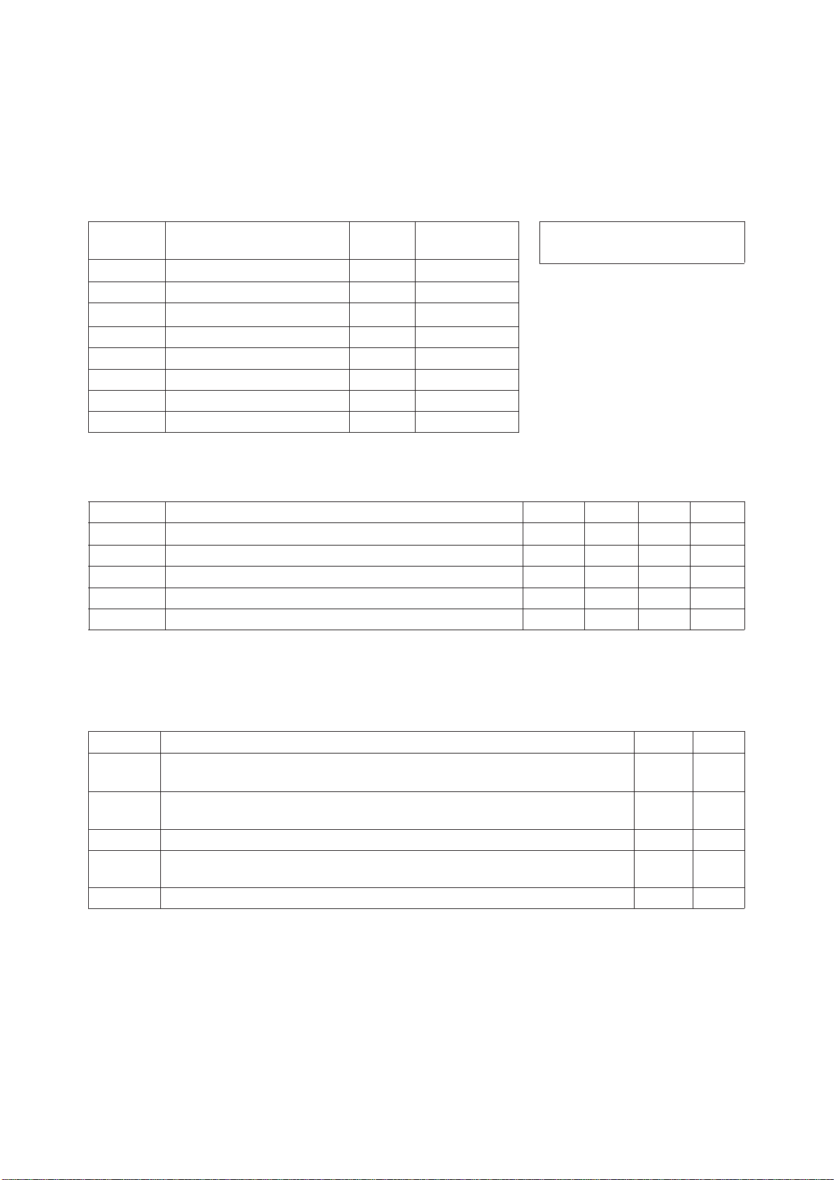
Figure 1. ATF-36077 Optimum Noise
Figure and Associated Gain vs.
Frequency for VDS = 1.5 V, ID = 10 mA.
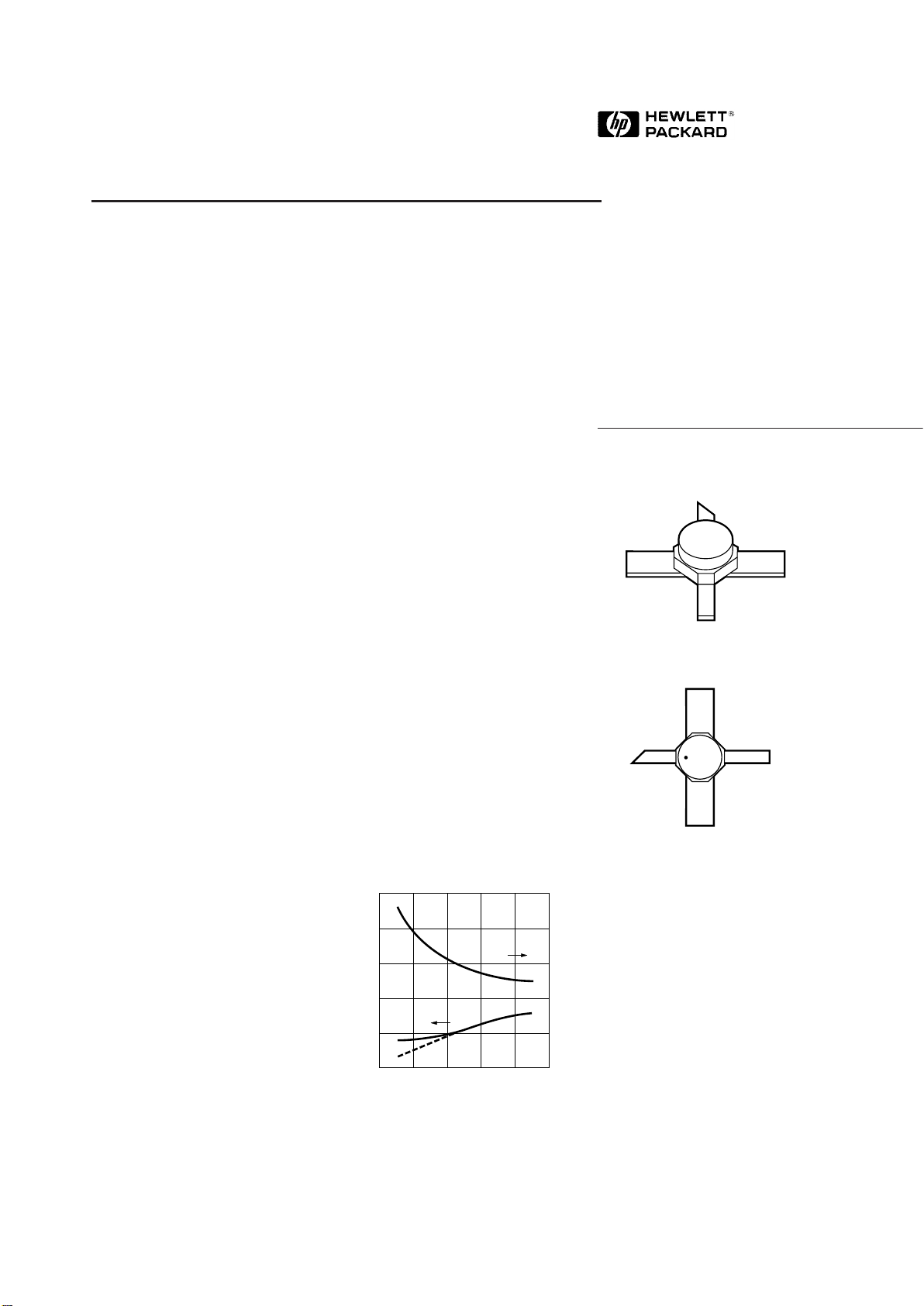
Pin Configuration
77 Package
NOISE FIGURE (dB)
0
0
FREQUENCY (GHz)
81620
1.2
0.8
0.4
4
12
Ga
ASSOCIATED GAIN (dB)
NF
10
15
20
25
[1]
Note: 1. See Noise Parameter Table.
Description
Hewlett-Packard’s ATF-36077 is
an ultra-low-noise Pseudomorphic
High Electron Mobility Transistor
(PHEMT), packaged in a low
parasitic, surface-mountable
ceramic package. Properly
matched, this transistor will
provide typical 12 GHz noise
figures of 0.5 dB, or typical 4 GHz
noise figures of 0.3 dB. Additionally, the ATF-36077 has very low
noise resistance, reducing the
sensitivity of noise performance
to variations in input impedance
match, making the design of
broadband low noise amplifiers
much easier. The premium
sensitivity of the ATF-36077
makes this device the ideal choice
for use in the first stage of
extremely low noise cascades.
The repeatable performance and
consistency make it appropriate
for use in Ku-band Direct Broadcast Satellite (DBS) Television
systems, C-band Television
Receive Only (TVRO) LNAs, or
other low noise amplifiers
operating in the 2-18␣ GHz
frequency range.
This GaAs PHEMT device has a
nominal 0.2 micron gate length
with a total gate periphery (width)
of 200 microns. Proven gold based
metalization systems and nitride
passivation assure rugged, reliable
devices.
5965-8726E
5-76
ATF-36077 Electrical Specifications,
T
C
= 25° C, ZO = 50 Ω, V
ds
= 1.5 V, Ids = 10 mA, (unless otherwise noted).
Symbol Parameters and Test Conditions Units Min. Typ. Max.
NF Noise Figure
[1]
f = 12.0 GHz dB 0.5 0.6
G
A
Gain at NF
[1]
f = 12.0 GHz dB 11.0 12.0
g
m
Transconductance VDS = 1.5 V, VGS = 0 V mS 50 55
I
dss
Saturated Drain Current VDS = 1.5 V, VGS = 0 V m A 15 25 45
V
p 10 %
Pinch-off Voltage VDS = 1.5 V, IDS = 10% of I
dss
V -1.0 - 0.35 - 0.15
Note:
1. Measured in a fixed tuned environment with Γ source = 0.54 at 156°; Γ load = 0.48 at 167°.
Thermal Resistance
[2,3]
:
θ
ch-c
= 60° C/W
Notes:
1. Operation of this device above any one
of these parameters may cause
permanent damage.
2. Measured at P
diss
= 15 mW and
T
ch
= 100°C.
3. Derate at 16.7 mW/°C for TC > 139°C.
ATF-36077 Absolute Maximum Ratings
Absolute
Symbol Parameter Units Maximum
[1]
V
DS
Drain – Source Voltage V +3
V
GS
Gate – Source Voltage V -3
V
GD
Gate-Drain Voltage V -3.5
I
D
Drain Current mA I
dss
P
T
Total Power Dissipation
[3]
mW 180
P
in max
RF Input Power dBm +10
T
ch
Channel Temperature °C 150
T
STG
Storage Temperature °C -65 to 150
ATF-36077 Characterization Information,
T
C
= 25° C, ZO = 50 Ω, V
ds
= 1.5 V, Ids = 10 mA, (unless otherwise noted).
Symbol Parameters and Test Conditions Units Typ.
NF Noise Figure (Tuned Circuit) f = 4 GHz dB 0.3
[2]
f = 12 GHz dB 0.5
G
A
Gain at Noise Figure (Tuned Circuit) f = 4 GHz dB 17
f = 12 GHz dB 12
S
12 off
Reverse Isolation f = 12 GHz, VDS = 1.5 V, VGS = -2 V dB 14
P
1dB
Output Power at 1 dB Gain Compression f = 4 GHz dBm 5
f = 12 GHz d Bm 5
V
GS 10 mA
Gate to Source Voltage for IDS = 10 mA VDS = 1.5 V V -0.2
Note:
2. See noise parameter table.
 Loading...