

Page 1
Service Manual
HP 8560A Spectrum Analyzer
SERIAL NUMBERS
Prefix
3207A
and Above
HEWLETT
Eiia
HP Part No. 08560-90081
Printed in USA
PACKARD
August 1992
Page 2

@Copyright Hewlett-Packard Company 1990, 1992
All Rights Reserved. Reproduction, adaptation, or translation without prior written
permission is prohibited, except as allowed under the copyright laws.
1212 Valley House Drive, Rohnert Park, CA 94928-4999, USA
Page 3

Certification
Hewlett-Packard Company certifies that this product met its published specifications at the
time of shipment from the factory. Hewlett-Packard further certifies that its calibration
measurements are traceable to the United States National Institute of Standards and
Technology, to the extent allowed by the Institute’s calibration facility, and to the calibration
facilities of other International Standards Organization members.
Warranty
This Hewlett-Packard instrument product is warranted against defects in material and
workmanship for a period of one year from date of shipment. During the warranty period,
Hewlett-Packard Company will, at its option, either repair or replace products which prove to
be defective.
For warranty service or repair, this product must be returned to a service facility designated
by HP. Buyer shall prepay shipping charges to HP and HP shall pay shipping charges to
return the product to Buyer. However, Buyer shall pay all shipping charges, duties, and taxes
for products returned to HP from another country.
HP warrants that its software and firmware designated by HP for use with an instrument
will execute its programming instructions when properly installed on that instrument. HP
does not warrant that the operation of the instrument, or software, or firmware will be
uninterrupted or error-free.
Limitation of Warranty
The foregoing warranty shall not apply to defects resulting from improper or inadequate
maintenance by Buyer, Buyer-supplied software or interfacing, unauthorized modification or
misuse, operation outside of the environmental specifications for the product, or improper
site preparation or maintenance.
NO OTHER WARRANTY IS EXPRESSED OR IMPLIED. HP SPECIFICALLY
DISCLAIMS THE IMPLIED WARRANTIES OF MERCHANTABILITY AND FITNESS
FOR A PARTICULAR PURPOSE.
Exclusive Remedies
THE REMEDIES PROVIDED HEREIN ARE BUYER’S SOLE AND EXCLUSIVE
REMEDIES. HP SHALL NOT BE LIABLE FOR ANY DIRECT, INDIRECT, SPECIAL,
INCIDENTAL, OR CONSEQUENTIAL DAMAGES, WHETHER BASED ON
CONTRACT, TORT, OR ANY OTHER LEGAL THEORY.
Assistance
Product maintenance agreements and other customer assistance agreements are available for
Hewlett-Packard products.
For any assistance, contact your nearest Hewlett-Packard Sales and Service
Ofice.
. . .
III
Page 4

Safety Symbols
The following safety symbols are used throughout this manual. Familiarize yourself with each
of the symbols and its meaning before operating this instrument.
Caution
Warning
The caution sign denotes a hazard. It calls attention to a procedure which,
if not correctly performed or adhered to, could result in damage to or
destruction of the instrument. Do not proceed beyond a caution sign until the
indicated conditions are fully understood and met.
The
warning
if not correctly performed or adhered to, could result in injury or loss of life.
Do not proceed beyond a
understood and met.
sign denotes a hazard. It calls attention to a procedure which,
warning
General Safety Considerations
Warning
Before this instrument is switched on,
through the protective conductor of the ac power cable to a socket outlet
provided with protective earth contact.
Any interruption of the protective (grounding) conductor, inside or outside
the instrument, or disconnection of the protective earth terminal can result in
personal injury.
sign until the indicated conditions are fully
make sure it has been properly grounded
Warning
Caution
There are many points in the instrument which can, if contacted, cause personal.
injury. Be extremely careful.
Any adjustments or service procedures that require operation of the instrument
with protective covers removed should be performed only by trained service
personnel.
Before this instrument is switched on, make sure its primary power circuitry
has been adapted to the voltage of the ac power source.
Failure to set the ac power input to the correct voltage could cause damage to
the instrument when the ac power cable is plugged in.
iv
Page 5

HP 8560A Spectrum Analyzer Documentation Outline
For ordering information, contact a Hewlett-Packard Sales and Service Office.
Manuals Shipped with Your Instrument
HP 8560A Installation and Verification Manual
n Tells you how to install the spectrum analyzer.
n Tells you what your analyzer’s specifications are.
0
HP
856OA/8561 B/8563A
w
Tells you how to make measurements with your spectrum analyzer.
w
Tells you how to program your spectrum analyzer.
perating
and Programming Manual
HP 8560A Quick Reference Guide
8
Is an abbreviated version of the HP
856OA/8561B/8563A
Operating and Programming
iWanua1
n Provides you with a listing of all remote programming commands.
Options
S
Option 915:
HP 8560A
ervice
Component Level Information
w
The service manual provides information to service your analyzer to the assembly-level (not
always immediately available for new products).
n The component-level information binder provides component-level information for
component-level repair of the analyzer or analyzer family (not always immediately available
for new products).
Manual and HP 8560A/6lB/63A Spectrum Analyzer
Option 910: Extra Manual Set
w
Doubles all documentation shipped with a standard instrument.
Option 916: HP 8560A Quick Reference Guide
1
Adds an extra HP 8560A Quick Reference Guide to the document package.
V
Page 6

Contents
1. General Information
Manual Organization
Manual Text Conventions
Serial Numbers Covered by This Manual
Instrument Variations
HP 85629B Test and Adjustment Module
Service Kit
Recommended Test Equipment
Electrostatic Discharge
Reducing Potential for ESD Damage
Static-Safe Accessories
Returning Instruments for Service
Service Tag
Original Packaging
Other Packaging
Sales and Service Offices
2. Adjustment Procedures
Introduction
Safety Considerations
Which Adjustments Should Be Performed?
Test Equipment
Adjustable and Factory-Selected Components
Adjustment Tools
Instrument Service Position
Using the TAM
Test Equipment
Adjustment Indicator
1. High-Voltage Power Supply Adjustment
2. Display Adjustment
3. IF
4. IF Amplitude Adjustments
5. DC Log Amplifier Adjustments
6. Sampling Oscillator Adjustment
7. YTO Adjustment
8. First LO Distribution Amplifier Adjustment
9. Tracking Generator Power Level Adjustments
10. Frequency Response Adjustment
11. Calibrator Amplitude Adjustment
12. 10 MHz Reference Adjustment (Non-Option 003 only)
13. Demodulator Adjustment
14. External Mixer Bias Adjustment
..............................
.............................
Bandpass
.........................
.......................
.................
.........................
................
.....................
........................
.................
........................
....................
............................
.........................
..........................
........................
........................
...............
...........................
..............
..........................
.....................
............................
...........................
........................
..............
......................
Adjustment
.......................
.....................
...................
.................
.................
............
...........
................
................
.......
....................
................
l-l
l-2
l-2
l-3
l-6
l-6
1-6
l-7
l-7
1-8
1-8
l-8
l-8
1-8
1-11
2-l
2-2
2-2
2-2
2-2
2-3
2-3
2-9
2-9
2-9
2-12
2-14
2-20
2-25
2-29
2-33
2-37
2-40
2-42
2-45
2-48
2-50
2-52
2-55
Contents-l
Page 7

15. External Mixer Amplitude Adjustment
16. Second IF Gain Adjustment
17. Signal ID Oscillator Adjustment
18. 600 MHz Amplitude Adjustment
19. 10 MHz Reference Adjustment (Option 003)
20. Tracking Oscillator Adjustment (Option 002)
3. Assembly Replacement
Access to Internal Assemblies
Cable Color Code
Procedure 1. Analyzer Cover
Procedure 2. Al Front Frame/Al8 CRT
Procedure 3.
Procedure 4.
Procedure 5. A2, A3, A4, and A5 Assemblies
Procedure 6. A6 Power Supply Assembly
Procedure 7.
Procedure 8. A7 through Al3 Assemblies
A7 1st LO Distribution Amplifier
A8 Low Band Mixer
A9 Input Attenuator
A10 Tracking Generator (Option 002)
AllYTO
Al3 Second Converter
Procedure 9. Al4 and Al5 Assemblies
Procedure 10. Al7 CRT Driver
Procedure 11. Bl Fan
Procedure 12.
Procedure 13. Rear Frame/Rear Dress Panel
Procedure 14. W3 Line Switch Cable
Procedure 15. EEROM (A2U501)
Procedure 16. A21 OCXO (Option 003)
...........................
AlAl
Keyboard/Front Panel Keys
AlA
RPG
A6Al
High Voltage Assembly
.........................
.............................
BTl
Battery
......................
.....................
......................
........................
........................
........................
.....................
..............
..................
.................
................
...........
...........
................
............
.............
...............
..............
...............
...................
.................
................
....................
..............
.................
..................
................
2-57
2-60
2-63
2-66
2-68
2-71
3-2
3-2
3-3
3-4
3-11
3-12
3-13
3-19
3-22
3-25
3-28
3-29
3-30
3-31
3-32
3-33
3-34
3-37
3-38
3-39
3-40
3-44
3-50
3-51
4. Replaceable Parts
Ordering Information
Direct Mail-Order System
Direct Phone-Order System
Parts List Format
Firmware-Dependent Part Numbers
5. Major Assembly and Cable Locations
Introduction . . . . . . . . . . . . . . . . . . . . . . . . . . . . . 5-l
Contents-2
.........................
...........................
......................
.....................
...................
4-l
4-l
4-2
4-2
4-2
Page 8

6. General Troubleshooting
Introduction .............................
Assembly Level Text
Block Diagrams
...........................
Assembly Test Points
........................
........................
Pad.. .............................
Test Jack
Ribbon Cables
WR PROT/WR ENA
Troubleshooting to a Functional Section
Using the TAM
Diagnostic Functions
TAM Requirements
Test Connectors
Revision Connectors
Inconsistent Results
Erroneous Results
............................
...........................
Softkey
Menus
.................
.................
............................
........................
.........................
..........................
........................
.........................
..........................
Blank Display ...........................
Automatic Fault Isolation
Display/Power Supply
Controller Check
ADC/Interface
IF/LOG Check
.........................
Check
..........................
LO Control Check
......................
.......................
.......................
........................
RF Check ............................
Manual Probe Troubleshooting
Cal Osc. Troubleshooting Mode
Error Messages
............................
Viewing Multiple Messages
Error Message Elimination
System Analyzer Programming Errors (100 to 150)
ADC Errors (200 to 299)
.......................
LO and RF Hardware/Firmware Failures (300 to 399)
YTO Loop Errors (300 to 301)
Roller PLL Errors (302 to 316)
YTO Loop Errors (317 to 318)
Roller Oscillator Errors (321 to 329)
YTO Loop Errors (331)
600 MHz Reference Loop (333)
YTO Leveling Loop (334)
Sampling Oscillator (335)
Automatic IF Errors (400 to 599)
System Errors (600 to 651)
Digital and Checksum Errors (700 to 799)
EEROM Checksum Errors (700 to 704)
Program ROM Check-sum Errors (705 to 710)
RAM Check Errors (711 to 719)
Microprocessor Error (717)
Battery Problem (718)
........................
Model Number Error (719)
System Errors (750 to 757)
....................
...................
......................
......................
...........
..........
...................
...................
...................
.................
......................
...................
.....................
.....................
...................
......................
...............
...............
............
..................
.....................
......................
......................
6-1
6-l
6-l
6-2
6-2
6-2
6-2
6-6
6-8
6-10
6-10
6-11
6-11
6-11
6-12
6-12
6-12
6-12
6-12
6-12
6-13
6-13
6-13
6-13
6-13
6-14
6-15
6-15
6-16
6-16
6-17
6-18
6-18
6-18
6-20
6-20
6-21
6-21
6-22
6-22
6-22
6-31
6-31
6-31
6-32
6-33
6-33
6-33
6-34
6-34
Contents-3
Page 9

Option Module Errors (800 to 899)
User-Generated Errors (902 to 904)
Block Diagram Description
RF Section .............................
A7 LODA ............................
A8 Low Band Mixer ........................
A9 Input Attenuator
All YTO
Al3 Second Converter
A15Al
Third Converter (P/O A15)
Flatness Compensation Amplifiers (P/O A15)
Synthesizer Section
Sweeping the First LO
Reference PLL (P/O A15)
YTO PLL (A7, All, P/O A14, P/O A15)
Offset Lock Loop (P/O A15)
Roller Oscillator PLL (P/O A14)
IF Section .............................
A4 LOG Amplifier/Cal Oscillator assembly
A5 IF Assembly
ADC/Interface
ADC ..............................
Log Expand/Video Functions (P/O A3)
Triggering ............................
Controller Section
EEROM
Firmware
Display ASM
Display/Power Supply Section
A6 Power Supply
Al7 CRT Display Driver
............................
Second IF Distribution Amplifier (P/O A15)
Section
..........................
.............................
............................
...........................
.......................
.......................
.......................
.........................
.......................
.....................
.........................
.......................
.........................
......................
..................
..................
..........
....................
............
..............
....................
..................
..............
...............
....................
6-34
6-34
6-35
6-36
6-36
6-36
6-36
6-36
6-37
6-37
6-37
6-37
6-37
6-37
6-38
6-38
6-38
6-39
6-39
6-40
6-40
6-41
6-42
6-42
6-42
6-42
6-43
6-43
6-43
6-43
6-43
6-43
7. ADC/Interface Section
Troubleshooting Using the TAM
Automatic Fault Isolation
Keyboard/RPG Problems
Keyboard Interface
RPG Interface
Triggering Problems
Flatness Control (RF Gain DACs)
A3 Assembly’s Video Circuits
Log Offset/Log Expand
Video MUX
Video Filter
Video Filter Buffer Amplifier
Positive/Negative Peak Detectors
Peak Detector Reset
Rosenfell Detector
ADCMUX
Variable Gain Amplifier (VGA)
Contents-4
.............................
....................
......................
.......................
.........................
...........................
..........................
...................
.....................
.......................
............................
............................
.....................
...................
.........................
.........................
....................
7-4
7-4
7-7
7-7
7-8
7-9
7-11
7-12
7-
14
7-15
7-15
7-16
7-17
7-18
7-18
7-19
7-21
Page 10

Track and Hold
A3 Assembly’s ADC Circuits
ADC Control Signals
ADC Start/Stop Control
ADC ASM
ADC ...............................
Ramp Counter
A3 Assembly’s Control Circuits
Analog Bus Drivers
Analog Bus Timing
Interface Strobe Select
8. IF Section
Troubleshooting Using the TAM
Troubleshooting A4 Log Amplifier with the TAM
Troubleshooting A5 with the TAM
Troubleshooting A4 Cal Oscillator with the TAM
Automatic IF Adjustment
Parameters Adjusted
Requirements
Performance Test Failures
IF Gain Uncertainty Performance Test
Scale Fidelity Performance Test
Resolution Bandwidths Performance Tests
A4 Assembly’s Log Amplifier Circuits
Log Amplifier
Linear Amplifiers
Video Offset
Video Output
Frequency Counter
AM/FM Demodulator
4.8 kHz IF Filters
4.8 kHz and 10.7 MHz IF Filters
10.6952 MHz VCXO
Input Switch
LO Switch
Synchronous Detector
Limiter
Isolation Amplifier
Detector/Mixer
Log Offset/Gain Compensation
Log Offset Compensation
Log Gain Compensation
Video Mux
A5 IF Section
IF Signature
Common IF Signature Problems
1 MHz Resolution Bandwidth Problems
30 kHz Resolution Bandwidth Problems
3 kHz and 10 kHz Resolution Bandwidth Problems
Step Gains
...........................
........................
.............................
...........................
.........................
.........................
........................
........................
............................
...........................
..........................
............................
...........................
Prescaler/Conditioner
.........................
..........................
.........................
............................
.............................
........................
.............................
........................
..........................
.............................
............................
............................
.............................
......................
.......................
.....................
....................
............
..................
............
.......................
.......................
.................
....................
...............
..................
...............
...................
....................
.....................
......................
...................
................
................
...........
7-21
7-22
7-22
7-23
7-24
7-24
7-25
7-26
7-26
7-27
7-28
8-3
8-4
8-4
8-8
8-9
8-10
8-11
8-12
8-12
8-13
8-13
8-14
8-14
8-15
8-16
8-16
8-17
8-17
8-17
8-18
8-19
8-19
8-19
8-20
8-20
8-20
8-20
8-21
8-21
8-21
8-21
8-22
8-23
8-28
8-30
8-32
8-32
8-33
Contents-5
Page 11

A4 Assembly’s Cal Oscillator Circuit
Cal Oscillator Unlock at Beginning of IF Adjust
Inadequate CAL OSC AMPTD Range
300 Hz to 3 kHz Resolution Bandwidth Out of Specification
Low-Pass Filter
Sweep Generator
AM/FM Demodulation, Audio Amplifier, and Speaker
9. Controller Section
Troubleshooting Using the TAM
Blank Display ...........................
Digital Signature Analysis (DSA)
Display Problems
Line Generators
Blanking
Display Jumbled or Trace Off Screen
Intensity ..............................
Bad Characters or Graticule
Long Lines Dimmer Than Short Lines
Analog Zero-Span Problems
Frequency-Count Marker Problems
Frequency Counter
State- and Trace-Storage Problems
Keyboard Problems
..............................
...........................
..........................
...........................
..........................
.....................
......................
..........................
..........................
..................
............
.................
.......
..........
....................
...............
.................
.................
...................
...................
....
:
8-34
8-35
8-35
8-36
8-40
8-40
8-40
9-l
9-2
9-4
9-4
9-4
9-5
9-7
9-10
9-10
9-11
9-12
9-13
9-14
9-15
9-16
10. Synthesizer Section
Confirming a Faulty Synthesizer Section
Troubleshooting Test Setup
Troubleshooting Using the TAM
General PLL Troubleshooting
PLL Locked at Wrong Frequency
Unlocked PLL
Frequency Span Accuracy Problems
Determining the First LO Span
Confirming Span Problems
YTO Main Coil Span Problems (LO Spans
YTO FM Coil Span Problems (LO Spans 1.01 MHz to 20 MHz)
Roller Oscillator Span Problems (LO Spans 51 MHz)
First LO Span Problems (All Spans)
Unlocked YTO PLL
Operation
Troubleshooting an Unlocked YTO PLL
Unlocked Roller Oscillator PLL
Operation
Confirming an Unlocked Condition
Offset Oscillator PLL
Transfer Oscillator PLL
Main Oscillator PLL
Unlocked Offset Lock Loop (Sampling Oscillator)
Operation
Troubleshooting
...........................
..........................
.............................
.............................
.............................
..........................
......................
....................
.....................
....................
......................
.....................
........................
.......................
........................
.................
...................
...................
>20
MHz)
.................
................
..................
.............
..........
.....
..........
10-2
10-7
10-8
10-13
10-13
10-13
10-15
10-15
lo-16
lo-16
10-17
lo-18
10-21
lo-23
lo-23
lo-25
lo-32
lo-32
lo-32
10-33
10-35
10-37
10-39
10-39
10-39
Contents-6
Page 12

Unlocked Reference PLL
Operation
Troubleshooting
Third LO Driver Amplifier
Sampler and Sampler IF
Sweep Generator Circuit
A21 OCXO (Option 003 only)
11. RF Section
Troubleshooting Using the TAM
Low Band Problems (50 Hz to 2.9 GHz)
Low Band Problems
A7 LODA (LO Distribution Amplifier)
A9 Input Attenuator
Al3 Second Converter
Al4 Frequency Control Assembly ....................
A7 LODA Drive
Al5 RF Assembly
Confirming a Faulty Third Converter
Confirming Third Converter Output
Third Converter
Flatness Compensation Control
Control Latches
SIG ID Oscillator
10 MHz Reference
A10 Tracking Generator (Option 002)
Block Diagram Description
Tracking Oscillator ........................
Upconverter ...........................
Pentupler ............................
Modulator ............................
Coupler .............................
Output Mixer
Output Amplifier .........................
Bias Board ............................
Output Goes Unleveled (ERR 900 or ERR 901)
Excessive Residual FM
Flatness Out-of-Tolerance
Vernier Accuracy Out-of-Tolerance
Harmonic/Spurious Outputs Too High
Power Sweep Not Functioning Properly
No Power Output
.............................
...........................
...........................
........................
..........................
......................
........................
........................
.....................
....................
.................
..........................
.................
.........................
.........................
..........................
.................
..................
..........................
....................
..........................
..........................
..................
......................
..........................
.............
.......................
......................
..................
.................
................
..........................
lo-42
lo-42
lo-42
10-44
10-45
10-47
lo-52
11-2
11-4
11-5
11-6
11-7
11-8
11-9
11-9
11-10
11-10
11-11
11-11
11-13
11-13
11-13
11-14
11-18
11-18
11-18
11-18
11-18
11-18
11-18
11-18
11-19
11-19
11-19
11-20
11-21
11-21
1 l-22
11-23
11-23
Contents-7
Page 13

12. Display/Power Supply Section
Troubleshooting Using the TAM
Blank Display
Blank Display
Display Distortion
Focus Problems
Intensity Problems
A6 Power Supply Assembly
Dead Power Supply
Line Fuse Blowing
Supply Restarting Every 1.5 Seconds (Kick Start)
Low Voltage Supplies
High Voltage Supplies
CRT Supply Dropping Out
Blanking Signal
Buck Regulator Control
DC-DC Converter Control
Power Up
A. Component-Level Information Packets
Index
...........................
............................
..........................
............................
..........................
.........................
.........................
........................
........................
...........................
.......................
.............................
....................
......................
......................
......................
............
12-4
12-5
12-6
12-7
12-8
12-9
12-11
12-11
12-13
12-13
12-13
12-14
12-15
12-15
12-16
12-16
12-17
Contents-8
Page 14
Figures
l-1. Serial Number Label Example
l-2. Example of a Static-Safe Workstation
1-3. HP 8560A Shipping Container and Cushioning Materials
2-1. High-Voltage Power Supply Adjustment Setup
2-2. Display Adjustment Setup
2-3. CRT Adjust Pattern
2-4. A2 Display Adjustment Locations
2-5. IF
2-6. IF Amplitude Adjustment Setup
2-7. IF Amplitude Adjustment Locations
2-8. Sampler Adjustment Setup
2-9. Coarse-Tune Adjustment Setup
2-10. YTO Adjustment Setup
2-11. First LO Distribution Amplifier Adjustment Setup
2-12. Tracking Generator Power Level Adjustments Setup and Adjustment
2-13. Frequency Response Adjustment Setup
2-14. Calibrator Amplitude Adjustment Setup
2-15. 10 MHz Frequency Reference Adjustment Setup
2-16. Demodulator Adjustment Setup
2-17. External Mixer Bias Adjustment Setup
2-18. External Mixer Amplitude Adjustment Setup
2-19. Location of
2-20. Signal ID Oscillator Adjustment Setup
2-21. 600 MHz Amplitude Adjustment Setup
2-22. 10 MHz Reference Adjustment (Option
2-23. Tracking Oscillator Adjustment Setup
3- 1.
3-2. Discharging the Post-Accelerator Cable
3-3. A9, A18, and Line-Switch Assembly Mounting Screws
3-4. Front-Frame Mounting Screws
3-5. Installing the CRT and Front-Frame Assemblies
3-6. Placing the CRT into the Front Frame
3-7. A2, A3, A4, and A5 Assembly Removal
3-8. Assembly Cables (1 of 2)
3-8. Assembly Cables (2 of 2)
3-9. Coaxial Cable Clip
3-10. HP-IB and
3-11. A6 Power Supply Connections
3-12. Power Supply Cover
3-13. Al7 CRT Driver Mounting Screws
3-14. Assembly Locations
Bandpass
Locations
Hinged Assemblies
Adjustment Setup
............................
A15Al
AlAl Wl
........................
.......................
.........................
.........................
.......................
.......................
.........................
Cable Placement
.........................
.........................
....................
.................
.........
.............
......................
...................
....................
...................
.................
......................
....................
...........
................
................
............
...................
................
..............
.................
................
003)/Setup
.................
................
....................
.................
................
................
....................
..................
and Adjustment Location
..........
............
l-2
1-7
l-10
2-12
2-14
2-17
2-18
2-20
2-25
2-26
2-33
2-35
2-37
2-40
2-43
2-45
2-48
2-50
2-52
2-55
2-57
2-61
2-63
2-66
2-69
2-72
3-3
3-5
3-6
3-7
3-8
3-9
3-14
3-15
3-16
3-17
3-18
3-20
3-21
3-23
3-26
Contents-9
Page 15

3-15. RF Section Bias Connections . . . . . . . . . . . . . . . . . . . . .
3-16. A9 Mounting Screws at Right Frame
3-17. A10 Tracking Generator Mounting Screws
3-18. All Mounting Screws
........................
3-19. Al4 and Al5 Assembly Removal
3-20. Al4 and Al5 Assembly Cables
3-21. Al7 Mounting Screws
3-22. Main Deck Screws
3-23. A6 Power-Supply Cover
........................
.........................
.......................
....................
3-24. W3 Dress and Connection to A6 Power Supply
3-25. Line Switch Mounting Screw and Cable Dress
3-26. W3 Cable Connector
3-27. Side Frame Mounting Screws
3-28. A21 OCXO Mounting Screws
........................
.....................
.....................
4-l. Parts Identification, Assembly Mounting
4-2. Parts Identification, Cover Assembly
4-3. Parts Identification, Main Chassis
4-4. Parts Identification, RF Section
....................
4-5. Parts Identification, Front Frame
4-6. Parts Identification, Rear Frame
5-
1. Hinged Assemblies
5-2. Top View (A2 Unfolded)
.........................
.......................
5-3. Top View (A2 and A3 Unfolded)
5-4. Top View (A2, A3, A4, and A5 Unfolded)
5-5. Bottom View (Al5 Unfolded)
.....................
5-6. Bottom View (Al5 and Al4 Unfolded)
5-7. Front End
5-8. Rear View
6-l. Assembly Test Points
.............................
.............................
........................
6-2. Ribbon Cable Connections (1 of 2)
6-3. WR ENA Softkey Menu
6-4. Functional Sections
6-5. Phase Lock Loops
..........................
6-6. Simplified Block Diagram
.......................
.........................
......................
6-7. HP 8560A Overall Block Diagram (Sheet 1 of 3)
6-7. HP 8560A Overall Block Diagram (Sheet 2 of 3)
6-7. HP 8560A Overall Block Diagram (Sheet 3 of 3)
7-l. A3 Test Connectors
.........................
7-2. A3 Interface Assembly Block Diagram
8-1. A4 and A5 Test Connectors
.....................
8-2. IF Section Troubleshooting with TAM
8-3. IF Adjust Signature
.........................
8-4. Detailed IF Adjust Signature (1)
8-5. Detailed IF Adjust Signature (2)
8-6. Detailed IF Adjust Signature (3)
8-7. Detailed IF Adjust Signature (4)
8-8. Detailed IF Adjust Signature (5)
8-9. Noisy Signature
8-10. Noise with Correct Shape
8-11. Region B Amplitude Variation
8-12. Region B Amplitude Offset
...........................
......................
....................
......................
.................
...............
...................
.............
.............
................
.................
...................
...................
...................
...................
...............
................
..................
............
............
............
.................
.................
...................
...................
...................
...................
...................
3-27
3-30
3-31
3-32
3-34
3-36
3-37
3-41
3-43
3-45
3-46
3-47
3-49
3-51
4-21
4-33
4-35
4-37
4-39
4-41
5-4
5-4
5-5
5-6
5-7
5-8
5-9
5-10
6-3
6-4
6-7
6-35
6-39
6-45
6-47
6-49
6-51
7-4
7-29
8-3
8-7
8-25
8-25
8-26
8-26
8-27
8-27
8-28
8-29
8-29
8-30
Contents-10
Page 16
8-13. Faulty Crystal Short
8-14. Faulty LC Pole
...........................
8-15. Faulty Crystal Symmetry
........................
......................
8-16. Output Waveform, 10 kHz Resolution Bandwidth
8-17. Output Waveform, 3 kHz Resolution Bandwidth
8-18. Output Waveform, 1 kHz Resolution Bandwidth
8-19. Output Waveform, 300 Hz Resolution Bandwidth
8-20. Failed Crystal Set Symptoms
8-21. A4 Log Amplifier Block Diagram
8-22. A5 IF Assembly Block Diagram
8-23. Cal Oscillator Block Diagram
9-l. A2 Test Connectors
.........................
9-2. Line Generator Output Waveforms
9-3. Blanking Waveforms
........................
9-4. Expanded Blanking Waveforms
9-5. Switch Driver Waveform LCHAR
9-6. Distorted X/Y Line Generator Waveforms
9-7. Expanded X/Y Line Generator Waveforms
9-8. Normal X/Y Line Generator Waveforms
9-9. Delta X Waveform
9-10.
Delta Y Waveform
9-
11.
DEFl
Synchronization
.........................
.........................
........................
9-12. A2 Controller Block Diagram
10-l. YTO Loop Test Setup
........................
10-2. Sampler and Sampling Oscillator Test Setup
10-3. Al4 and Al5 Test Connectors
10-4. PLL Locked at Wrong Frequency
10-5. Unlocked PLL
...........................
10-6. Input to YTO FM Coil Driver
10-7. Input to
Main/FM/VCO
10-8. Troubleshooting an Unlocked YTO PLL
10-9.
Simplified Sweep Generator
10-10. Simplified Sweep Generator during Retrace
10-11. Simplified Synthesizer Section
10-12. Simplified Al4 Assembly Block Diagram
10-13. Simplified Al5 Assembly Block Diagram
10-14. Frequency Control Block Diagram
10-15. RF Assembly Block Diagram
11-l. Al4 and Al5 Test Connectors
11-2. A7 LODA Drive
..........................
11-3. 10 MHz Reference at A15J302
11-4. 10 MHz TTL-Reference at
.....................
...................
....................
.....................
..................
....................
...................
...............
...............
................
.....................
..............
....................
...................
....................
Sweep Switch
................
................
.....................
...............
....................
................
................
...................
.....................
....................
....................
U303
Pin 5
.................
11-5. HP 8560A RF Section Troubleshooting Block Diagram
12-l. Simplified Section Block Diagram
12-2. Al7 Test Connector
12-3. Probe Power Socket
12-4. Buck Regulator Waveform
.........................
.........................
......................
12-5. A6 Power Supply Block Diagram
12-6. Al7 CRT Driver Block Diagram
A-l. Interconnect Diagram
........................
...................
...................
...................
............
............
............
............
.........
8-31
8-31
8-33
8-37
8-38
8-38
8-39
8-39
8-43
8-45
8-47
9-3
9-5
9-6
9-7
9-8
9-9
9-9
9-10
9-11
9-12
9-13
9-17
10-5
10-6
10-8
10-13
10-14
lo-18
10-19
lo-26
10-47
lo-48
10-49
10-50
10-51
10-53
10-54
11-2
11-10
11-15
11-16
11-25
12-2
12-5
12-7
12-12
12-19
12-21
A-7
Contents-l 1
Page 17

Tables
l-l. Service Kit Contents
l-2. Static-Safe Accessories
l-3. Hewlett-Packard Sales and Service Offices
1-4. Recommended Test Equipment
2-l. Related Adjustments (1 of 2)
2-l. Related Adjustments (2 of 2)
2-2. Adjustable Components (1 of 3)
2-2. Adjustable Components (2 of 3)
2-2. Adjustable Components (3 of 3)
2-3. Factory Selected Components
2-4. TAM Adjustments
2-5. Required Test Equipment for TAM
2-6. Factory-Selected LC Filter Capacitors
2-7. LC Factory-Selected Capacitor Selection
2-8. Factory-Selected XTAL Filter Capacitors
2-9. XTAL Factory-Selected Capacitor Selection
2-10. Capacitor Part Numbers
2-11. Sampling Adjustments
2-12. Conversion Loss Data
2-13. A15U802 Values
2-14. Tracking Oscillator Range Centering
3-l. Required Tools ...........................
4-2. Reference Designations, Abbreviations and Multipliers (1 of 4)
4-2. Reference Designations, Abbreviations, and Multipliers (2 of 4)
4-2. Reference Designations, Abbreviations, and Multipliers (3 of 4)
4-2. Reference Designations, Abbreviations, and Multipliers (4 of 4)
4-3. Manufacturers Code List (1 of 3)
4-4. Replaceable Parts
6-l. Location of Assembly Troubleshooting Text
7-l. W2 Control Cable Connections (1 of 2)
7-2. Automatic Fault Isolation References
7-3. TAM Tests Versus A3 Test Connectors
7-4. Keyboard Matrix
7-5. Counter Frequencies
7-6. Trigger MUX Truth Table
7-7. A3U102 Latch Outputs
7-8.
HMUX-SELO/l
7-9. Logic Levels at A3U108
7-10. Demultiplexer A3U410 Truth Table
7-11. Demultiplexer A3U500 Truth Table
8-l. Automatic Fault Isolation References
8-2. TAM Tests Versus Test Connectors (1 of 2)
8-3. Sweep Width Settings
Versus Detector Mode
........................
........................
...............
....................
.....................
.....................
...................
...................
...’................
.....................
.........................
..................
.................
................
...............
..............
.......................
........................
........................
..........................
.................
......
......
......
......
...................
..........................
..............
.................
.................
................
..........................
.........................
......................
.......................
................
.......................
..................
..................
.................
..............
........................
l-6
l-8
1-12
1-13
2-4
2-5
2-6
2-7
2-8
2-8
2-10
2-10
2-22
2-22
2-23
2-23
2-24
2-36
2-59
2-62
2-73
3-2
4-3
4-4
4-5
4-6
4-7
4-10
6-9
7-2
7-5
7-6
7-7
7-9
7-9
7-16
7-18
7-20
7-28
7-28
8-4
8-5
8-9
Contents-12
Page 18

8-4. Available Reference Level Range
8-5. Signal Level for Reference Level Display
9-l. TAM Tests Versus Test Connectors
9-2. Gate Times
10-l. Center Frequency Tuning Values
10-2. Sampling Oscillator Test Frequencies
10-3. YTO Frequency in TEST Position
10-4. Automatic Fault Isolation References (1 of 2)
10-4. Automatic Fault Isolation References (2 of 2)
10-5. TAM Tests versus Test Connectors (1 of 2)
10-5. TAM Tests versus Test Connectors (2 of 2)
10-6. Sweep Signal Destination versus Span
10-7. Harmonic Mixing Number versus Center Frequency
10-8. Settings of Sweep Switches
10-9.
Settings of Sweep Switches
10-10. Settings for Switches and Comparators
lo-
11. Amplifier Polarities
10-12. YTO Frequency Errors with A14J23 on Pins 2 and 3
10-13. Voltages in FM Coil and Main Loop Drivers
10-14. Main Coil Coarse and Fine DACs Voltages
10-15. Sampling Oscillator PLL Divide Ratios
11-1. Automatic Fault Isolation References
11-2. TAM Tests versus Test Connectors
11-3. Attenuator Pin Values
11-4. RF Section Mnemonic Table
12-1. Wl Power-Cable Connections (1 of 2)
12-1. Wl Power-Cable Connections (2 of 2)
12-2. Automatic Fault Isolation References
12-3. TAM Tests versus Test Connectors
A-l. HP 8560A Spectrum Analyzer Documented Assemblies
A-2. A4 and Al6 Assemblies Shipped with HP 8560As Serial Prefixed below 3207A
A-3. Al5 RF Assemblies Shipped with HP 8560As Serial Prefixed below 3029A .
............................
......................
......................
.........................
........................
...................
................
..................
...................
.................
..................
..............
..............
...............
...............
.................
...........
................
..........
..............
...............
................
.................
..................
.....................
.................
.................
.................
....,.............
.........
8-12
8-12
9-2
9-
14
10-3
10-7
10-8
10-9
10-10
10-11
10-12
10-15
10-15
10-17
10-19
10-22
lo-25
lo-28
10-30
10-31
10-40
11-3
11-4
11-7
11-17
12-3
12-4
12-4
12-5
A-2
A-4
A-5
Contents-13
Page 19

General Information
This HP 8560A Spectrum Analyzer Service Manual contains information required to adjust
and service the HP 8560A Spectrum Analyzer to the assembly level.
For component-level information, refer to the HP
Component Level Information.
856OA/61B/63A
Spectrum Analyzer
Manual Organization
Chapter 1, General Information, contains information about service kit contents,
recommended test equipment, returning an instrument for service, and sales and service
offices.
Chapter 2, Adjustment Procedures, contains the necessary adjustment procedures to adjust
the instrument properly after repair.
Chapter 3, Assembly Replacement, contains instructions for removal and replacement of all
major assemblies.
Chapter 4, Replaceable Parts, contains the information necessary to order parts or assemblies
for the instrument.
Chapter 5, Major Assembly and Cable Locations, contains figures identifying all major
assemblies and cables.
Chapter 6, General Troubleshooting, contains instrument-level troubleshooting information,
block diagrams, and troubleshooting information covering the instrument’s six functional
areas.
Chapters 7 through 12 contain troubleshooting information covering the instrument’s six
functional areas.
Appendix contains the component-level documented assemblies matrix and the HP 8560A
Interconnect Diagram.
General Information
1-l
Page 20

Manual Text Conventions
The following text conventions are used throughout this manual:
m
Softkeys
Display
Text
Serial
This service manual applies directly to HP 8560A spectrum analyzers with serial numbers
prefixed 3207A and above. For HP 8560A spectrum analyzers with serial numbers prefixed
below
Hewlett-Packard makes frequent improvements to its products to enhance their performance,
usability, or reliability. HP service personnel have access to complete records of design changes
to each type of equipment, based on the equipment’s serial number. Whenever you contact
HP about your analyzer, have the complete serial number available to ensure obtaining the
most complete and accurate information possible.
3207A, order HP Part Number 08560-90038.
Boxed text in this typeface represents a mechanical key physically located on the
instrument.
Shaded text indicates a
activated by pressing corresponding keys surrounding the display. The labels
displayed are determined by the mechanical front-panel key depressed and the
instrument’s firmware.
Text printed in this typeface indicates text appearing on the screen.
N.umbers
Covered by This Manual
softkey. Softkey labels appear on the display and can be
The serial number label is attached to the rear of the analyzer. The serial number has two
parts: the prefix (the first four numbers and a letter), and the suffix (the last five numbers).
See Figure l-l.
The first four numbers of the prefix are a code identifying the date of the last major design
change incorporated in your analyzer. The letter identifies the country in which the unit
was manufactured. The five-digit suffix is a sequential number and is different for each
unit. Whenever you list the serial number or refer to it in obtaining information about your
analyzer, be sure to use the complete number, including the full prefix and the suffix.
Figure l-l. Serial Number Label Example
l-2 General Information
Page 21

Instrument Variations
The following text lists the unique assemblies contained in the HP 8560A Options 001, 002,
003, and all combinations.
HP 8560A Option 001 (Rear-Panel 2nd IF Output)
Al5 RF Assembly
w19
Rear-panel JlO
HP 8560A Option 002 (Tracking Generator)
A10 Tracking Generator
Al5 RF Assembly
Front dress-panel
w14
W16
W36
W42
w43
W46
w47
W48
unique part number
added
added
added
unique part number
unique part number
added
added
deleted
deleted
added
added
added
added
Rear-panel J 11
Front-panel
Front-panel J6
HP 8560A Option 012 (001 + 002)
Al5 RF Assembly unique part number
w19
Rear-panel JlO
A10 Tracking Generator
Front dress-panel
w14 added
W16
W36
W42 deleted
w43
53
added
deleted
added
added
added
added
unique part number
added
deleted
added
General Information 1-3
Page 22

W46
added
w47
W48
Rear-panel J 11
Front-panel
Front-panel J6
HP 8560A Option 003 (Precision Frequency Reference)
Al5 RF Assembly
A21 OCXO
w49
w50
HP 8560A Option 013 (001 + 003)
Al5 RF Assembly
w19
Rear-panel JlO
53
added
added
added
deleted
added
unique part number
added
added
added
unique part number
added
added
A21 OCXO
w49
w50
HP 8560A Option 023 (002 + 003)
Al5 RF Assembly
A10 Tracking Generator
Front dress-panel
w14
W16
W36
W42
w43
W46
w47
W48
added
added
added
unique part number
added
unique part number
added
added
deleted
deleted
added
added
added
added
Rear-panel
Front-panel
1-4 General Information
Jll
53
added
deleted
Page 23

Front-panel J6
added
A21 OCXO
w49 added
w50
HP 8560A Option 123 (001 + 002 + 003)
Al5 RF Assembly
w19
Rear-panel JlO
A10 Tracking Generator
Front dress-panel
w14
W16
W36
W42
w43
W46
added
added
unique part number
added
added
added
unique part number
added
added
deleted
deleted
added
added
w47
W48
Rear-panel
Front-panel J3
Front-panel J6
A21 OCXO
w49
w50
Jll
added
added
added
deleted
added
added
added
added
General Information l-5
Page 24

HP 85629B Test and Adjustment Module
When attached to the spectrum analyzer’s rear panel, the HP 85629B Test and Adjustment
p
Module (TAM)
rovides diagnostic functions for the HP 8560A. Because the TAM connects
directly to the analyzer’s internal data and address bus, it controls the analyzer’s hardware
directly. It would be impossible to control the hardware to the same extent either from the
analyzer’s front panel or over the HP-IB.
The TAM measures voltages at key points in the circuitry and flags a failure whenever the
voltage falls outside the limits. The TAM locates the failure to a small functional area which
can be examined manually.
Service Kit
The HP 8560A Service Kit (HP part number 08562-60021)
contains service tools required to
repair the instrument. Refer to Table l-l for a list of items in the service kit.
Table l-l. Service Kit Contents
Description
Cable Puller
PC Board Prop
Line Filter Assembly
Line Switch Cable
Extender Cable
BNC to SMB (snap-on) Cable
Connector Extractor Tool Kit
Quantity
1
1
1
1
1
2
1
HP Part Number
5021-6773
5021-7459
5061-9032
5062-0728
5062-0737
85680-60093
8710-1791
Recommended Test Equipment
Equipment required for operation verification, performance tests, adjustments,
troubleshooting, and the Test and Adjustment Module is listed in Table l-4. Other equipment
may be substituted if it meets or exceeds the critical specifications listed in the table. Refer to
the HP 856OA Installation and Verification Manual for the performance tests.
1-6 General Information
Page 25
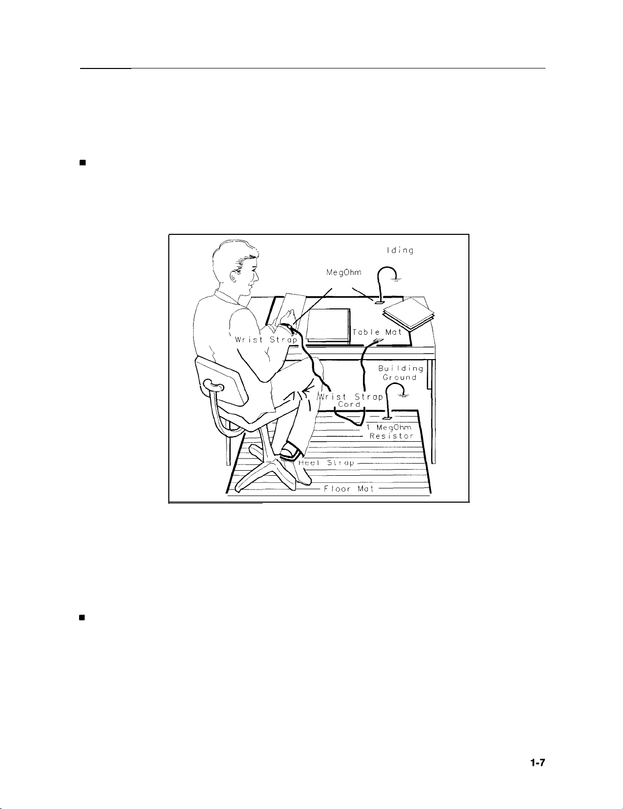
Electrostatic Discharge
Electrostatic discharge (ESD)
can damage or destroy electronic components. Therefore,
all work performed on assemblies consisting of electronic components should be done at a
static-free workstation. Figure l-2 is an example of a static-safe work station using two kinds
of ESD protection:
w
Conductive table mat and wrist-strap combination.
n Conductive floor mat and heel-strap combination.
These methods may be used together or separately.
Bui
lding
Ground
1
MegOhm
Resistor
I /TV
hhirist
StroD\
*
5111125
Figure 1-2. Example of a Static-Safe Workstation
Reducing Potential for ESD Damage
The suggestions that follow may help reduce ESD damage that occurs during
testing and servicing.
w
Before connecting any coaxial cable to an analyzer connector for the first time each day,
momentarily ground the center and outer connectors of the cable.
n Personnel should be grounded with a resistor-isolated wrist strap before touching the center
in of any connector and before removing any assembly from the unit.
n Be sure all instruments are properly earth-grounded to prevent build-up of static discharge.
General Information
nstrument
l-7
Page 26

Static-Safe Accessories
Table 1-2. Static-Safe Accessories
HP Part
Number
9300-0797
9300-0980
9300-1383
9300-l169
ESD heel-strap (reusable 6 to 12 months).
Set includes: 3M static control mat 0.6 m x 1.2 m (2 ft x 4 ft) and 4.6 cm (15 ft)
ground wire. (The wrist-strap and wrist-strap cord are not included. They must
be ordered separately.)
Wrist-strap cord 1.5 m (5 ft)
Wrist-strap, color black, stainless steel, without cord, has four adjustable links
and a 7 mm post-type connection.
Description
Returning Instruments for Service
Service Tag
If you are returning the instrument to Hewlett-Packard for servicing, fill in and attach a blue
service tag. Service tags are supplied in the back of this chapter.
Please be as specific as possible about the nature of the problem. If you have recorded any
error messages that appeared on the screen, or have completed a performance test record, or
have any other specific data on the performance of the analyzer, please send a copy of this
information with the unit.
Original Packaging
Before shipping, pack the unit in the original factory packaging materials if they are available.
If the original materials are unavailable, identical packaging materials may be acquired
through’any Hewlett-Packard Sales and Service Office. Descriptions of the packaging materials
are listed in Figure l-3.
Other Packaging
Caution
Repackage the analyzer in the original packaging materials or with commercially available
materials described in steps 4 and 5, below.
1. Attach a completed service tag to the instrument.
1-8 General Information
Analyzer damage can result from using packaging materials other than those
specified. Never use styrene pellets in any shape as packaging materials. They
do not adequately cushion the equipment or prevent it from shifting in the
carton. They cause equipment damage by generating static electricity and by
lodging in the analyzer fan.
Page 27

2. Install the front-panel cover on the instrument.
3. Wrap the instrument in antistatic plastic to reduce the possibility of damage caused by
electrostatic discharge.
4. Use the original materials or a strong shipping container that is double-walled, corrugated
cardboard carton with 159 kg (350 lb)
ursting strength. The carton must be both large
b
enough and strong enough to accommodate the analyzer and allows at least 3 to 4 inches
on all sides of the analyzer for packing material.
5. Surround the equipment with at least 3 to 4 inches of packing material, or enough to
prevent the equipment from moving in the carton. If packing foam is unavailable, the best
TM
alternative is SD-240 Air Cap
Air Cap looks like a plastic sheet covered with
from Sealed Air Corporation (Commerce, CA 90001).
l-1/4
inch air-filled bubbles. Use the
pink-colored Air Cap to reduce static electricity. Wrap the equipment several times in this
material to both protect the equipment and prevent it from moving in the carton.
6. Seal the shipping container securely with strong nylon adhesive tape.
7. Mark the shipping container
“FRAGILE, HANDLE WITH CARE” to assure careful
handling.
8. Retain copies of all shipping papers.
General Information
l-9
Page 28
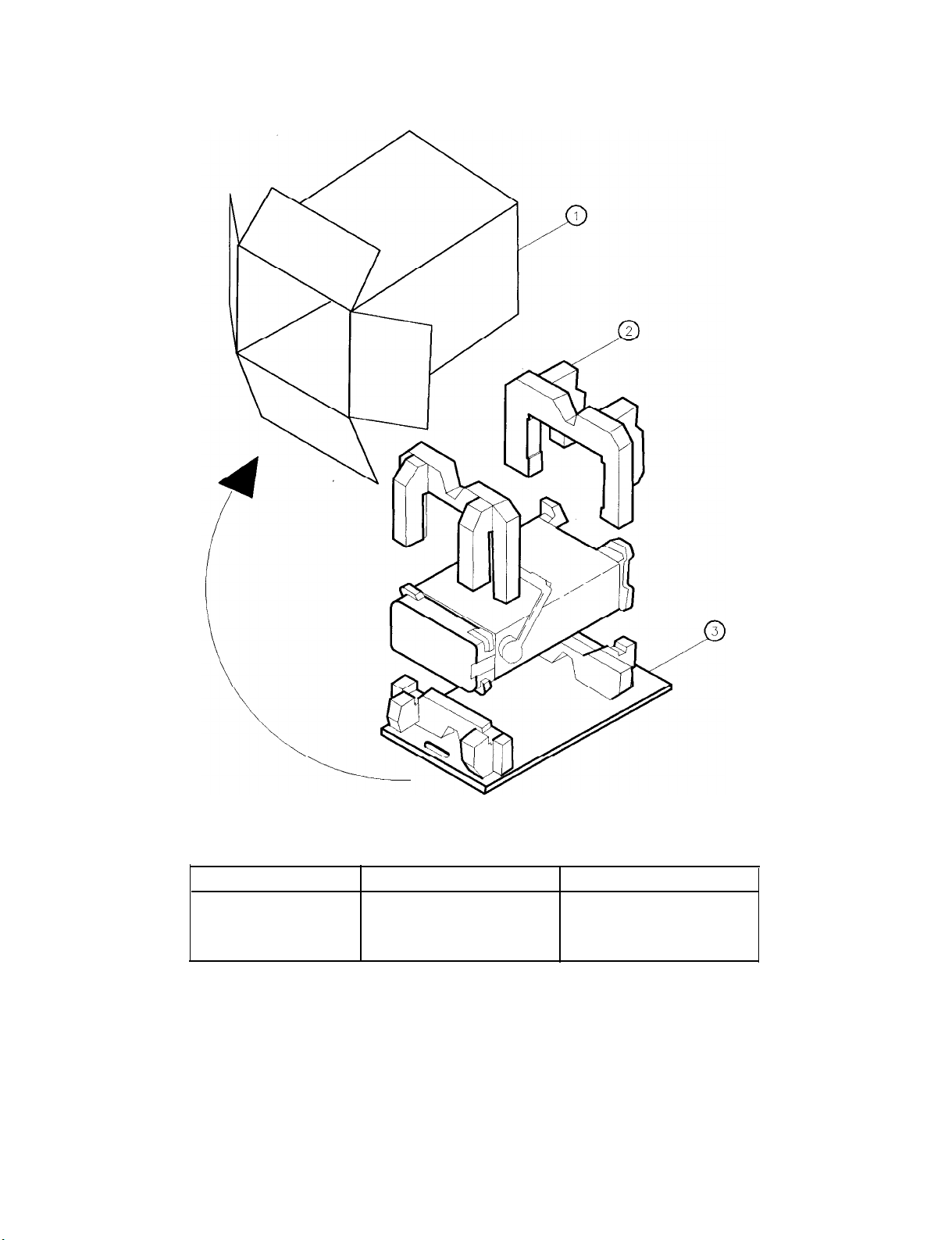
SK1126
Item
1
2
3
Figure 1-3. HP 8560A Shipping Container and Cushioning Materials
l-1 0 General Information
Description
9211-5636
08590-80013
08590-80014
HP Part Number
Outer Carton
Pads (2)
Bottom Tray
Page 29

Sales and Service Offices
Hewlett-Packard has sales and service offices around the world providing complete support for
Hewlett-Packard products. To obtain servicing information, or to order replacement parts,
contact the nearest Hewlett-Packard Sales and Service Office listed in Table l-3.
In any correspondence, be sure to include the pertinent information about model numbers,
serial numbers, and assembly part numbers.
Note
Within the USA, a toll-free phone number is available for ordering
replacement parts. Refer to the “Ordering Information” section in Chapter 4,
“Replaceable Parts,” for the phone number and more information.
General Information l-l 1
Page 30
Table 1-3. Hewlett-Packard Sales and Service Offices
US FIELD OPERATIONS EUROPEAN OPERATIONS
HEADQUARTERS
HEADQUARTERS
Hewlett-Packard Company Hewlett-Packard S.A.
19320 Pruneridge Avenue
Cupertino, CA 95014, USA 1217 Meyrin
(800) 752-0900
150, Route du Nant-d’Avri1
2/Geneva
Switzerland
(41 22) 780.8111
California
Hewlett-Packard Co.
France
1421 South Manhattan Ave. Hewlett-Packard France
Fullerton, CA 92631
(714) 999-6700
1 Avenue Du Canada Blackburn, Victoria 3130
Zone
D’Activite
De Courtaboeuf (61 3) 895-2895
F-91947 Les Ulis Cedex
Hewlett-Packard Co.
301 E. Evelyn
France
(33 1) 69 82 60 60
Mountain View, CA 94041
(415) 694-2000
Colorado
Hewlett-Packard Co.
24 Inverness Place, East
Englewood, CO 80112
Germany
Hewlett-Packard
GmbH
Berner Strasse 117 Canada
6000 Frankfurt 56
West Germany
(49 69) 500006-O
(303) 649-5000
Great Britain
Georgia
Hewlett-Packard Co.
2000 South Park Place
Atlanta, GA 30339
(404) 955-1500
IlklOiS
Hewlett-Packard Ltd.
Eskdale Road, Winnersh Triangle Kanagawa 229, Japan
Wokingham, Berkshire
RGll
England
(44 734) 696622
Hewlett-Packard Co.
5201 Tollview Drive
Rolling Meadows, IL 60008
(708) 255-9800
New Jersey
Hewlett-Packard Co.
120 W. Century Road
Paramus, NJ 07653
(201) 599-5000
Texas
Hewlett-Packard Co.
930 E. Campbell Rd.
Richardson, TX 75081
(214) 231-6101
INTERCON OPERATIONS
HEADQUARTERS
Hewlett-Packard Company
3495 Deer Creek Rd.
Palo Alto, California 94304-1316
(415) 857-5027
Australia
Hewlett-Packard Australia Ltd.
31-41 Joseph Street
Canada
Hewlett-Packard (Canada) Ltd.
17500 South Service Road
Trans-Canada Highway
Kirkland, Quebec H9J 2X8
(514) 697-4232
Japan
Yokogawa-Hewlett-Packard Ltd.
1-27-15 Yabe, Sagamihara
5DZ (81 427) 59-1311
China
China Hewlett-Packard, Co.
38
Bei
San Huan Xl Road
Shuang Yu Shu
Hai Dian District
Beijing, China
(86 1) 256-6888
Singapore
Hewlett-Packard Singapore
Pte. Ltd.
1150 Depot Road
Singapore 0410
(65) 273 7388
Taiwan
Hewlett-Packard Taiwan
8th Floor, H-P Building
337 Fu Hsing North Road
Taipei, Taiwan
(886 2) 712-0404
1-12 General Information
Page 31

Table 1-4. Recommended Test Equipment
Instrument
Synthesized
Sweeper
(two required)
Synthesizer/
Level Generator
Synthesized
Signal Generator Residual SSB Phase Noise at 10 kHz offset
Pulse/Function Frequency Range: 10 kHz to 50 MHz HP 8116A
Generator
AM/FM
Signal Generator
Microwave Frequency Range: 9 MHz to 6.9 GHz
Frequency Counter Time base Accuracy (Aging): <5 x
Universal
Counter
Oscilloscope
Spectrum Analyzer
* Part of Microwave Workstation
P
=
Performance Tests; A = Adjustments; M = Test & Adjustment Module; T = Troubleshooting;
V = Operation Verification
Frequency Range: 10 MHz to 7
Frequency Accuracy (CW): 1 x
Leveling Modes: Internal & External
Modulation Modes: AM & Pulse
Power Level Range: -80 to
Frequency Range: 200 Hz to 80 MHz
Frequency Accuracy: 1 x
Flatness: f0.15 dB
Attenuator Accuracy: <&0.09 dB
Frequency Range: 5 MHz to 2.5
(320 MHz <fc <640 MHz): <-131 dBc/Hz
Pulse Width: 200 ns;
Output Amplitude: 5 V peak-to-peak
Functions: Pulse
TTL Sync Output
Frequency Range: 1 MHz to 200 MHz HP 8640B
Frequency Modulation Mode
Modulation Oscillator Frequency: 1
FM Peak Deviation: 5 kHz
External Frequency Reference Input
Modes: TI
Time Interval Measurement Range: 20 ms to 75 s
Frequency Measurement Range: 17
Frequency Resolution: 1 MHz at 10 MHz
External Frequency Reference Input
Time base accuracy (Aging):
Bandwidth (3
Minimum Vertical Deflection Factor: <2 mV/div
Frequency Range: 4
Typical Residual FM: <l Hz Pk-to-Pk in 100 ms
(Fundamental Mixing)
Critical Specifications
for Equipment Substitution
GHz
10eg/day
+16 dBm
10e7/month
GHz
&
Triangle
kHz
lo-“/day
AFB, Frequency Count
kHz to 11 MHz
<3
x
10m7/month
dB): dc to 100 MHz
kHz to 7 GHz
of
Recommended Use
Model
8340A*
HP
HP
3335A*
HP 8663A
HP
5343A*
Option 001
HP
5334A/B
HP
1980A/B* A,T
HP
8566A/B
P,A,M,V
P
PAT,
M,V
PAT,
M,V
p,v
P
A
PAT
General Informationl- 13
Page 32

Table 1-4. Recommended Test Equipment (continued)
Instrument
Measuring
Receiver
Power Sensor
Power Sensor
Power Sensor
4mplifier
Digital Voltmeter Range: -15 V dc to +120 V dc
DVM Test Leads
10 dB Step Attenuation Range: 30 dB
Attenuator Frequency Range: dc to 80 MHz
1 dB Fixed Attenuation Range: 12 dB
Attenuator
’
Part of Microwave Workstation
P = Performance Tests; A = Adjustments; M = Test & Adjustment Module; T = Troubleshooting
V = Operation Verification
Compatible w/Power Sensors
dB Relative Mode
Resolution: 0.01 dB
Reference Accuracy: <&1.2%
Frequency Range: 50 MHz to 6.9 GHz
Maximum SWR:
1.15 (2.0 to 6.5 GHz)
Frequency Range: 250 MHz to 350 MHz
Power Range: 100 nW to 10
Maximum SWR: 1.15 (250 to 350 MHz)
Frequency Range: 100 kHz to 2.9 GHz HP 8482A*
Maximum SWR:
1.1 (1 MHz to 2.0 GHz)
1.30 (2.0 GHz to 2.9 GHz)
Frequency Range: 2.0 to 2.9 GHz HP 11975
Minimum Output Power (Leveled)
2.0 to 8.0 GHz: $16
Output SWR (Leveled):
Accuracy:
Input Impedance: 21
236
Connectors: BNC (f)
Frequency Range: dc to 80 MHz
Connectors: BNC (f)
Critical Specifications
for Equipment Substitution Model
1.15 (50 to 100 MHz)
1.10 (100 MHz to 2 GHz)
1.20 (12.4 to 18 GHz)
PW
dBm
<1.7
<fl
mV on 10 V Range
Ma
inches, alligator clips, probe tips
Recommended Use
HP
8902A*
HP
8485A*
HP 8484A
HP
3456A*
HP 34118A
HP 355D
HP 355C
PAT,
M,V
PAT,
M,V
P,A
PAT,
M,V
P
A
A,T
p,v
P,V,A
1-14 General Information
Page 33

Table 1-4. Recommended Test Equipment (continued)
Instrument
20 dB Fixed
Attenuator
Frequency Range: dc to 6.5 GHz
Attenuation Accuracy:
Critical Specifications
for Equipment Substitution
<fl
dB
Recommended
Model
HP 8491B
Option 020
Use
p,v
Maximum SWR: 1.2 (dc to 6.5 GHz)
10 dB Fixed
Attenuator
Frequency Range: dc to 6.5 GHz
Attenuation Accuracy:
<f0.6
dB
HP 8491B
Option 010
p,v
Maximum SWR: 1.2 (dc to 6.5 GHz)
Signature Multimeter
Reference Attenuator
Termination
Clock Frequency
>lO
MHz
Supplied with HP 8484A
Frequency Range: dc to 22 GHz
Impedance:
Maximum SWR:
5OQ
<1.22
HP
5005A/B
HP 11708A
HP
909D
T
P,A
P,M,V
Connector: APC 3.5
Low-Pass Filter
Cutoff Frequency: 50 MHz
0955-0306
P,M,V
Rejection at 80 MHz: >50 dB
12 MHz Low-Pass-Filter Cutoff Frequency: 12 MHz
0955-0518
P
g-element Tchebychev, 0.1 dB ripple
Rejection at 18 MHz: >45 dB
Directional
Bridge
Frequency Range: 5 MHz to 50 MHz
Coupling: 6.0 dB (nominal)
HP 8721A
P
Directivity: 30 dB minimum
Power Splitter
VSWR:
Frequency Range: 1 kHz to 22 GHz
<1.45
HP 11667B
P,A,M,V
Insertion Loss: 6 dB (nominal)
Output Tracking:
Equivalent Output SWR:
Product Support Kit No Substitute
Adapter
Type N (f) to BNC (m)
Adapter Type N (m) to BNC (f)
(three required)
Adapter
Adapter
Adapter
(two required)
Adapter
Type N (f) to BNC (f)
Type N (f) to APC 3.5 (m)
Type N (m) to APC 3.5 (m)
Type N (m) to APC 3.5 (f)
<0.25
dB
<1.22
08562-60021
1250-1477
1250-1476
1250-
1474
1250-1750 A
1250-1743
P,A,M,V
1250-1744
A,T
A
p,v
p,v
P,A,V
P = Performance Tests; A = Adjustments; M = Test & Adjustment Module; T = Troubleshooting;
V = Operation Verification
General Information 1-15
Page 34

Table 1-4. Recommended Test Equipment (continued)
ment Substitution
Type N (m) to SMA (f)
Length:
Cable,
Cable, HP-IB
5052
Coaxial Connectors: BNC (m)
(five
required)
Length: 2 122 cm (48 in.)
Required w/Performance Test Software
(12 required) Required w/HP 85629B Test
291
cm (36 in.)
&
Adjustment Module
HP 10503A
HP 10833B
P,A,V
PAM
Length: 2 m (6.6 ft.)
Cable Frequency Range: 10 kHz to 6.9 GHz
(three required) Maximum SWR:
<1.4
at 6.9 GHz
8120-4921
P,A,M,V
Maximum Insertion Loss: 2 dB
Connectors: APC 3.5 (m), both ends
Length: 2 91 cm (36 in.)
Photometer/
No Substitute
JlG-TV
A
Tek
Radiometer
Controller
Required to run Operation Verification Software
No substitute.
HP 9816A,
HP
9836A/C,
V
or HP 310
Power Supply
Tuning Tool
Output Voltage:
224
V dc
Output Voltage Accuracy:
N/A
<f0.2
HP 6114A
V
8710-1010
A
A
P = Performance Tests; A = Adjustments; M = Test & Adjustment Module; T = Troubleshooting
V = Operation Verification
1-16 General Information
Page 35

Adjustment Procedures
Introduction
This chapter contains information on automated and manual adjustment procedures for the
HP 8560A spectrum analyzer. Perform the automated procedures using the HP 85629B
Tests and Adjustment Module (TAM). N
Adjustments should be performed after a repair or performance test failure.
Introduction
Safety Considerations
Which Adjustments Should Be Performed? ..........................................
Test Equipment
Adjustable and Factory-Selected Components ........................................
Adjustment Tools
Instrument Service Position
Using the TAM
Test Equipment ....................................................................
Adjustment Indicator ..............................................................
1. High-Voltage Power Supply Adjustment .........................................
2. Display Adjustment
3. IF
4. IF Amplitude Adjustments
5. DC Log Amplifier Adjustments
6. Sampling Oscillator Adjustment ................................................
7. YTO Adjustment
8. First LO Distribution Amplifier Adjustment
9. Tracking Generator Power Level Adjustments
10. Frequency Response Adjustment
11. Calibrator Amplitude Adjustment
12. 10 MHz Reference Adjustment (Non-Option 003 only)
13. Demodulator Adjustment
14. External Mixer Bias Adjustment ..............................................
15. External Mixer Amplitude Adjustment ........................................
16. Second IF Gain Adjustment
17. Signal ID Oscillator Adjustment ...............................................
18. 600 MHz Amplitude Adjustment ..............................................
19. 10 MHz Reference Adjustment (Option 003)
20. Tracking Oscillator Adjustment
.........................................................................
..............................................................
....................................................................
..................................................................
........................................................
.......................................................................
..........................................................
Bandpass
Adjustment .......................................................
.....................................................
.............................................................
....................................................
.................................................
perform adjustments as routine maintenance.
ever
................................................
....................................
..................................
..............................................
.............................................
.........................
.................................. .2-68
...............................................
..2- 2
..2- 3
..2- 9
..2-14
.2-29
..2-3 7
.2-42
.2-45
..2-5 2
.2-55
..2-6 0
.2-71
2
..2-
.2-2
..2- 2
.2-2
..2- 3
.2-9
..2- 9
.2-12
2-20
2-25
2-33
.2-40
2-48
.2-50
.2-57
2-63
.2-66
1
Note
Before performing any adjustments, allow the instrument to warm up for 5
minutes.
Adjustment Procedures
2-l
Page 36

Safety Considerations
Although this instrument has been designed in accordance with international safety standards,
this manual contains information, cautions, and warnings which must be followed to ensure
safe operation and to prevent damage to the instrument. Service and adjustments should be
performed only by qualified service personnel.
Warning
Warning
Warning
Warning
Adjustments in this section are performed with power supplied to the instrument
and protective covers removed. There are voltages at many points in the
instrument which can, if contacted, cause personal injury. Be extremely careful.
Adjustments should be performed only by trained service personnel.
Power is still applied to this instrument with the m switch in the off position.
Before removing or installing any assembly or printed circuit board, remove the
line-power cord.
Capacitors inside the instrument may still be charged, even if the instrument has
been disconnected from its source of supply.
Use a nonmetallic adjustment tool whenever possible.
Which Adjustments Should Be Performed?
Table 2-1 lists the manual adjustments that should be performed when an assembly is repaired
or changed. It is important to perform the adjustments in the order indicated to ensure that
the instrument meets its specifications.
Test Equipment
The equipment required for the manual adjustment procedures is listed in Table 1-4,
“Recommended Test Equipment
given in the table may be substituted for the preferred test equipment.
Any equipment that satisfies the critical specifications
.”
Adjustable and Factory-Selected Components
Table 2-2 lists the adjustable components by reference designation and name. For each
component, the table provides a description and lists the adjustment number.
Refer to Table 2-3 for a complete list of factory-selected components used in the instrument
along with their functions.
schematic diagrams.
2-2 Adjustment Procedures
Factory-selected components are identified with an asterisk on the
Page 37

Adjustment Tools
For adjustments requiring a nonmetallic tuning tool, use fiber tuning tool, HP part number
8170-0033. For adjustments to the IF Bandpass, use tuning tool, HP part number 8710-1010.
Never try to force an adjustment control. This is especially critical when tuning variable
capacitors or slug-tuned inductors.
Required service accessories, with part numbers, are listed in “Service Kit” in Chapter 1.
Instrument Service Position
Refer to Chapter 3 for information on removing the analyzer cover assembly and accessing all
internal assemblies.
Adjustment Procedures 2-3
Page 38

Table 2-1. Related Adjustments (1 of 2)
Assembly Changed
or Repaired
AlAl
Keyboard
AlA
RPG
A2 Controller
A3 Interface
A4 Log Amp/Cal Osc
A5 IF
A6 Power Supply
A6Al
HV Module
A7
1ST
LO
Distribution Amplifier
A8 Low Band Mixer
A9 Input Attenuator
A10 Tracking Generator
All YTO
Perform the Following Related Adjustments in the Order Listed
No related adjustment
No related adjustment
Display Adjustment
If the old EEROM cannot be used in a new A2
or if an EEROM must be replaced, the following
adjustments must be performed:
External Mixer Amplitude Adjustment
Frequency Response Adjustment
Display Adjustment (Fast Zero Span)
Frequency Response Adjustment
Display Adjustment (Fast Zero Span)
Demodulator Adjustment
IF Amplitude Adjustment
DC Log Amplifier Adjustment
IF
Bandpass
Adjustment
IF Amplitude Adjustment
High Voltage Power Supply Adjustment
Display Adjustment
High Voltage Power Supply Adjustment
Display Adjustment
First LO Distribution Amplifier Adjustment
Frequency Response Adjustment (or perform the Frequency
Response performance test in the
HP 8560A Installation and Verification Manual.
The adjustment must be performed if the performance test fails.)
Frequency Response Adjustment
Frequency Response Adjustment (or perform the Frequency
Response performance test in the
HP 856OA Installation and Verification Manual.
The adjustment must be performed if the performance test fails.)
Tracking Generator Power Level Adjustment
Frequency Response Adjustment
YTO Adjustment
Frequency Response Adjustment (or perform the Frequency
Response performance test in the
HP 8560A Installation and Verification Manual.
The adjustment must be performed if the performance test fails.)
kdjustment
Number
2
15
10
2
10
2
13
4
5
3
4
1
2
1
2
8
10
10
10
9
10
7
10
2-4 Adjustment Procedures
Page 39

Table 2-1. Related Adjustments (2 of 2)
Assembly Changed
or Repaired
Al3 2nd Converter
Al4 Frequency Control
Al5 RF
Al5Al
2nd IF Amplifiel
Al5A2 Sampler
Al7 CRT Driver
Perform the Following Related Adjustments in the Order Listed
Frequency Response Adjustment
Display Adjustment (Fast Zero Span)
YTO Adjustment
First LO Distribution Amplifier Adjustment
Frequency Response Adjustment
10 MHz Reference Adjustment (TCXO)
Calibrator Amplitude Adjustment
External Mixer Bias Adjustment
Sampling Oscillator Adjustment
Signal ID Oscillator Adjustment
External Mixer Amplitude Adjustment
Frequency Response Adjustment
600 MHz Amplitude Adjustment
Second IF Gain Adjustment
Sampling Oscillator Adjustment
Display Adjustment
Adjustmeni
Number
10
2
7
8
10
12
11
14
6
17
15
10
18
16
6
2
418Vl
CRT
A19 HP-IB
A21 OCXO
Display Adjustment
No related adjustment
10 MHz Reference Adjustment (OCXO)
2
19
Adjustment Procedures 2-5
Page 40

Table 2-2. Adjustable Components (1 of 3)
Reference
Designator
A2R206
A2R209
A2R215
A2R218
A2R262
A2R263
A2R268
A2R271
A4C707
A4R445
A4R531
A4R544
A4R826
A5L300
A5L301
A5L700
A5L702
A5R343
A5T200
A5T202
Adjustment
Name
DGTL X GAIN
SWEEP OFFSET
DGTL Y GAIN
VIDEO OFFSET
STOP BLANK
START BLANK
VIDEO GAIN
SWEEP GAIN
FM DEMOD
LIMITER PHASE
LOG AMP TOS
LIN FIDELITY BOW
CAL OSC AMPTD
LC CTR 1
LC CTR 2
LC CTR 3
LC CTR 4
15 DB ATT
XTAL CTR 1
XTAL CTR 2
Adjustment
Number
2
2
2
2
2
2
2
2
13
5
5
5
4
3
3
3
3
4
3
3
Description
Adjusts the horizontal gain in the X line generator.
Adjusts the beginning of the trace to the leftmost
vertical graticule line in fast-analog, zero-span mode.
Adjusts the vertical gain in the Y line generator.
Adjusts the vertical position in fast-analog, zero-span
to match the digital zero-span input.
Adjusts the blanking at the end of a vector on
the display.
Adjusts the blanking at the start of a vector on
the display.
Adjusts the vertical gain in fast-analog, zero-span
to match with the digital zero-span input.
Adjusts the end of the trace to the rightmost
vertical-graticule line in fast-analog,
zero-span mode.
Adjusts the FM demodulation for a peak response.
Adjusts Limiter Phase for peak response
Minimizes Log error near Top of Screen
Minimizes Linearity Fidelity error.
Sets calibration oscillator output power
(nominally -35
the IF during the AUTO IF ADJUST routines.
Adjusts center frequency of first stage of LC
bandwidth filter to 10.7 MHz.
Adjusts center frequency of second stage of LC
bandwidth filter to 10.7 MHz.
Adjusts center frequency of third stage of LC
bandwidth filter to 10.7 MHz.
Adjusts center frequency of fourth stage of LC
bandwidth filter to 10.7 MHz.
Adjusts the attenuation of the Reference 15 dB
attenuator for 15 db between minimum and
maximum attenuation.
Adjusts center frequency of first stage of crystal
bandwidth filter to 10.7 MHZ.
Adjusts center frequency of second stage of crystal
bandwidth filter to 10.7 MHZ.
dBm).
This power is injected into
2-6 Adjustment Procedures
Page 41

Table 2-2. Adjustable Components (2 of 3)
Reference
Designatol
A5T500
A5T502
A6R410
AlOR
AlOR
AlOC3
A14R42
A14R76
A14R93
A14R621
414R628
415ClOO
A15C210
A15C629
A15R237
Adjustment
Name
XTAL CTR 3
XTAL CTR 4
HV ADJ
-10 dB ADJ
3 dB ADJ
TRK
OSC CTR
5.01 GHz
FM SPAN
3.2
GHz
;O
AMPTD
>ATE BIAS
;MPL
MATCH 1
VCO RANGE
298 MHz ADJ
SMPL PWR ADJ
Adjustmend
Number
3
3
1
9
9
20
7
7
7
8
8
6
6
17
6
Description
Adjusts center frequency of third stage of crystal
bandwidth filter to 10.7 MHz.
Adjusts center frequency of fourth stage of crystal
bandwidth filter to 10.7 MHz.
Adjusts the voltage between
to the voltage marked on the
Module.
Offsets power level range of A10 Tracking
Generator.
Adjusts gain of power level range of A10
Tracking Generator.
Centers range of A10 Tracking Generator’s
tracking oscillator.
Adjusts the main coil tune driver current at a
YTO frequency of 6.01 GHz (near the upper YTO
frequency limit).
Adjusts the FM span accuracy by affecting the
sensitivity of the FM coil driver.
Adjusts the main coil fixed driver current at a
YTO frequency of 3.2 GHz (near the lower
YTO frequency limit).
Adjusts the amplitude of the first LO by changing
the reference voltage for the leveling loop.
Adjusts the gate bias for the A7 LO Distribution
Amplifier.
Transforms the sampler input impedance to 50 ohms
3ver
the 280 to 298 MHz range.
Adjusts the VCO tank capacitance so that 21 V
on the VCO tune line equals 298 MHz VCO frequency.
Fine adjusts the 298 MHz SIG ID Oscillator
frequency to optimize its performance.
Adjusts the signal power level to the Sampler.
A6TP405
A6Al
and A6TP401
High Voltage
A15U302
A15R453
A15R726
10 MHz ADJ
PHASE DET
BIAS
500
MHz
4MPLITUDE
12
6
18
Adjusts frequency of the temperature
compensated crystal oscillator (TCXO) to 10 MHz.
Adjusts bias at pin 3 of phase detector A15U408 to
Adjusts input power to ECL divide-by-two chip.
Adjustment Procedures 2-7
1.80 V.
Page 42

Table 2-2. Adjustable Components (3 of 3)
Reference
Designator
A15R561
A15R926 EXT BIAS ZERO
A17R4 Z GAIN
A17Rll
A17R21
A17R26
A17R34
A17R55
A17R57
Al7R75
A17R77
A17R90
A17R92
417R93
Adjustment Adjustment Description
Name
CAL AMPTD
CUTOFF
Z FOCUS
X FOCUS
COARSE FOCUS
X GAIN
X POSN
Y GAIN
Y POSN
TRACE ALIGN
DDD
ASTIG
Number
11
14
2
2
2
2
2
2
2
2
2
2
2
2
Adjusts amplitude of the 300 MHz calibrator signal
to -10.0
Adjusts zero bias point of external mixer bias.
Adjusts maximum intensity.
Adjusts intensity to turn off blanked lines.
Adjusts focus for lines of different brightness.
Adjusts focus at the left and right corners of the display
Adjusts focus at the center of the display.
Adjusts the horizontal-deflection amplifier gain.
Adjusts the CRT horizontal position.
Adjusts the vertical-deflection amplifier gain.
Adjusts the CRT vertical position.
Adjusts the display axis rotation.
Adjusts focus of the center of the display.
Adjusts for the spot roundness on the CRT display.
dBm.
Reference Adjustment
Designator Number
A5C204
A5C216
A5C326
A5C327
A5C505
A5C516
A5C717
A5C718
A15U802
3
3
3
3
3
3
3
3
16
Table 2-3. Factory Selected Components
Basis of Selection
Selected to optimize center frequency of LC tank that loads the crystal.
Selected to optimize center frequency of LC tank that loads the crystal.
Selected to optimize LC pole center frequency.
Selected to, optimize LC pole center frequency.
Selected to optimize center frequency of LC tank that loads the crystal.
Selected to optimize center frequency of LC tank that loads the crystal.
Selected to optimize LC pole center frequency.
Selected to optimize LC pole center frequency.
Selected to set the gain of the second IF to 12 dB.
2-6 Adjustment Procedures
Page 43

Using the TAM
The HP 85629B TAM can be used to perform approximately half of the HP 8560A
adjustment procedures. Table 2-4 lists the TAM adjustments and their corresponding manual
adjustments.
The TAM adjustments do not include procedures for choosing factory-selected components. If
an adjustment cannot be made and a factory-selected component must be changed, refer to
the corresponding manual adjustment.
To select an adjustment, press
Position the pointer next to the desired adjustment using either the knob or step keys. Press
EXECUTE, then follow the on-screen instructions displayed.
(m)
to display the TAM Main Menu, then press ADJUST.
Test Equipment
During the TAM adjustments, instructions for setting test equipment controls are displayed,
with the exclusion of the test listed below. Test equipment for this adjustment is controlled
automatically.
Test 8. Low Band Flatness
Table 2-5 lists the test equipment needed to perform each TAM adjustment. Required models
must be used. Substitutions may be made for recommended models. Substitute sources
must operate over the frequency ranges indicated. Recommended substitutes are listed in
the Configuration Menu. If you must substitute the source with a user-defined model, the
adjustments run faster using a synthesized source rather than an unsynthesized source.
Note
When connecting signals from the HP
to the adjustment setup, use a high-frequency test cable with minimum
attenuation to 22 GHz. HP part number 8120-4921 is recommended for its
ruggedness, repeatability, and low insertion loss.
8340A/B
(or any microwave source)
Adjustment Indicator
To aid in making adjustments, the TAM displays an “Analog Voltmeter Display Box” along
the left-hand side of the display. A horizontal line moves inside the box to represent the
needle of an analog voltmeter. A digital readout appears below the box. Tick marks are often
displayed on the inside edges of the box indicating the desired needle position. (The tick
marks and needle are intensified when the needle is within this acceptable region.) During
some adjustments, an arrow appears along the right edge of the box. This arrow always
indicates the highest position the needle has reached. The arrow is useful when a component
must be adjusted for a peak response; if the peak is overshot, the arrow indicates where the
peak was. The component can be readjusted until the needle is at the same position as the
arrow.
Adjustment Procedures 2-9
Page 44

Table 2-4. TAM Adjustments
TAM Adjustment
1. IF Bandpass, LC Poles
2. IF Bandpass, Crystal Poles
3. IF Amplitude
4. Limiter Phase
5. Linear Fidelity
6. Log Fidelity
7. Sampling Oscillator
8. YTO YTO Adjustment
9. LO Distribution Amp
10. Low Band Flatness
11. Calibrator Amplitude Calibrator Amplitude Adjustment
12. 10 MHz Reference Oscillator 10 MHz Reference Adjustment - TCXO
13. External Mixer Bias *
14. External Mixer Amplitude * External Mixer Amplitude Adjustment
*
Adjustment excluded if the HP 8560A is an Option 002.
IF
IF
IF Amplitude Adjustment
DC Log Amplifier Adjustments, A4 Limiter Phase
DC Log Amplifier Adjustments, A4 Linear Fidelity
DC Log Amplifier Adjustments, A4 Log Fidelity
Sampling Oscillator Adjustment
First LO Distribution Amplifier Adjustment
Frequency Response Adjustment
External Mixer Bias Adjustment
Corresponding Manual Adjustment
Bandpass
Bandpass
(Option 003)
Adjustment
Adjustment
Adjustment
Number
3
3
4
5
5
5
6
7
8
10
11
19
14
15
Table 2-5. Required Test Equipment for TAM
Adjustment
1. IF
Bandoass.
2. IF Bandpass, Crystal Poles None
3. IF Amplitude Synthesizer/Level Generator HP 3335A
4. Limiter Phase
5. Linear Fidelity
LC Poles
Equipment Used Required Recommended
Model Model
None
Test Cable (SMB to BNC)
Manual Probe Cable
Synthesizer/Level Generator HP 3335A
Test Cable BNC
Synthesizer/Level Generator HP 3335A
Test Cable BNC
85680-60093
HP 10503A
HP 10503A
2-10 Adjustment Procedures
Page 45

Table 2-5. Required Test Equipment for TAM (continued)
Adjustment
6. Log Fidelity
7. Sampling Oscillator
8. YTO
9. LO Distribution Amplifier Power Meter
10. Low Band Flatness
11. Calibrator Amplitude
12. 10 MHz Reference
Oscillator
13. External Mixer Bias
14. External Mixer Amplitude Power Meter
Synthesizer/Level Generator HP 3335A
Test Cable BNC
Manual Probe Cable
Frequency Counter (3 to 6.8 GHz)
Power Sensor
(3 to 6.8 GHz, 10 to 20
Source (10 MHz to 2.9 GHz)
Power Meter
Power Sensor
(10 MHz to 2.9 GHz)
Power Splitter
(10 MHz to 2.9 GHz)
Power Meter
Power Sensor
Frequency Counter
(9 to 11 MHz)
Manual Probe Cable
Power Sensor
(310.7 MHz,
Source (310.7 MHz, -30
Equipment Used Required
-25 to -35
dBm)
dBm)
dBm)
Model
HP 8482A,
HP
8481A
Recommended
Model
HP 10503A
HP 5342A, HP 5343A
HP 8902A, HP 436A,
HP 438A
HP 8485A
HP
8340A/B
HP 8902A, HP 436A,
HP438A
HP 8482A, HP
HP 11667B
HP 8902A, HP 436A,
HP 438A
HP 5342A, HP 5343A
HP 8902A, HP 436A,
HP 438A
HP 8484A
HP
8340A/B
8481A
Adjustment Procedures 2-11
Page 46

1. High-Voltage Power Supply Adjustment
Assembly Adjusted
A6 Power Supply
Related Performance Test
There is no related performance test for this adjustment.
Description
The high-voltage power supply is adjusted to the voltage marked on the
The
A6Al
HV Module is characterized in the factory to ensure that the display filament
voltage is set to 6.0 V rms when the
on the HV Module.
Warning
Warning
Note
Note
To minimize shock hazard, use a nonmetallic adjustment tool when adjusting the
A6 Power Supply.
The following procedure probes voltages that, if contacted, could cause
personal injury or death.
Adjustment of the high-voltage power supply should not be a routine
maintenance procedure. Any adjustments should be done only if the A6 Power
Supply,
You must perform the display adjustments after this adjustment if either the
display or HV Module has been replaced.
A6Al
HV Module, or Al8 CRT (display) is repaired or replaced.
+llO
Vdc (
nominal) supply is set to the voltage marked
A6Al
HV Module.
DIGITAL VOLTMETER
Figure 2-1. High-Voltage Power Supply Adjustment Setup
2-12 Adjustment Procedures
SK11
Page 47

1. High-Voltage Power Supply Adjustment
Equipment
Digital Multimeter . . . . . . . . . . . . . . . . . . . . . . . . . . . . . . . . . . . . . . . . . . . . . . HP 3456A
DVM Test Leads . . . . . . . . . . . . . . . . . . . . . . . . . . . . . . . . . . . . . . . . . . . . . . . HP 34118A
Procedure
Warning
1. Set the HP 8560A (LINE) switch off, disconnect the power cord, and remove the analyzer
cover. Fold down the A2 Controller, A3 Interface, A4 Log Amplifier, and A5 IF assemblies.
Remove the A6 Power Supply cover.
2. Position the HP 8560A as shown in Figure 2-l. Connect the positive DVM lead to
A6TP405
3. Set the HP 3456A controls as follows:
FUNCTION . . . . . . . . . . . . . . . . . . . . . . . . . . . . . . . . . . . . . . . . . . . . . . . . DCVOLTS
RANGE . . . . . . . . . . . . . . . . . . . . . . . . . . . . . . . . . . . . . . . . . . . . . . . . . . .
4. Reconnect the power cord to the HP 8560A and set the
5. Record the voltage marked on the
6. Adjust A6R410 HV ADJ for a voltage equal to the voltage recorded in step 5.
7. Set the HP 8560A (LINE) switch off and disconnect the power cord. Wait at least 30 seconds
for the high-voltage power supply capacitors to discharge.
After disconnecting the ac power cord, allow capacitors in the high-voltage
supply to discharge for at least 30 seconds before removing the protective
cover from the A6 Power Supply.
and the negative DVM lead to
A6Al
A6TP401.
1OOOVOLTS
@
switch on.
HV Module.
Voltage marked on A6Al HV Module =
Vdc
8. Disconnect the DVM test leads from A6TP401 and
cover.
A6TP405.
Reinstall the power supply
Adjustment Procedures2- 13
Page 48

2. Display Adjustment
Assembly Adjusted
A2 Controller
Al7 CRT Driver
Related Performance Test
Sweep Time Accuracy (Sweep Times
<30
ms)
Description
Coarse adjustment of the deflection amplifiers, Z-axis amplifiers, and line generators is done
using the CRT adjust pattern.
amplitude adjustments correct for differences between analog and digital display modes. The
displayed sweep time accuracy is adjusted in the fast zero-span sweep adjustments.
Fine adjustments use the graticule. The fast zero-span
SPECTRUM
ANALYZER
BNC CABLE
SK12
Figure 2-2. Display Adjustment Setup
Equipment
10 dB VHF Step Attenuator
Photometer/Radiometer
.......................................
.......................................
Adapters
Type N (m) to BNC (f) . . . . . . . . . . . . . . . . . . . . . . . . . . . . . . . . . . . . . . . . . . . 1250-1476
Cables
BNC, 122 cm (2 required)
. . . . . . . . . . . . . . . . . . . . . . . . . . . . . . . . . . . . . . . HP 10503A
2-14 Adjustment Procedures
HP 355D
TEK
JlG-TV
Page 49

Procedure
2. Display Adjustment
1. Set the analyzer’s
@
switch off. Remove the analyzer’s cover and fold out the A2
Controller and A3 Interface assemblies as illustrated in Figure 2-2. Connect the CAL
OUTPUT to the INPUT. Adjustment locations are shown on the CRT neck for Al7
adjustments and in Figure 2-4 for the A2 adjustments.
Preliminary Adjustments
2. Set A17R55 X GAIN, A17R75 Y GAIN, A17R92 DDD, A17R93 ASTIG, A2R206 DGTL
X GAIN, A2R215 DGTL Y GAIN, A2R262 STOP BLANK, and A2R263 START
BLANK to midrange. Also set the rear-panel X POSN, Y POSN, and TRACE ALIGN to
midrange.
3. Set A17R21 Z FOCUS, A17R26 X FOCUS, and
A17Rll
CUTOFF fully counterclockwise.
4. Set A17R4 Z GAIN fully clockwise.
5. Turn the analyzer on and allow it to warm up for at least 3 minutes. Adjust
A17Rll
CUTOFF until the display is visible and A17R34 COARSE FOCUS for best possible
focus.
Cutoff Adjustment
6. Press
(=I,[-),
FOCUS
,127[=],
INTENSITY,255[jK$,
STORE FOCUS
,then
STORE INTENSITY, MORE I of 2,
GRAT OFF.
Adjust
A17Rll
CUTOFF until the
line between the bottom of trace A and the annunciators at the bottom of the display just
disappears.
Deflection Adjustments
7.
Press CRAT ON, MORE 2 of 2,
MORE
1
of 2 , and CRT ADJ PATTERN . Fold up the A3 Interface assembly.
8. Refer to Figure 2-3 for locating the lines used for adjusting DGTL X GAIN and DGTL Y
GAIN. Each of these lines is actually two lines adjusted for coincidence. The two lines will
form an “X” if they are not adjusted properly.
9. Adjust A2R206 DGTL X GAIN until the two vertical lines near the left edge of the
display appear to be one single line.
10. Adjust A2R215 DGTL Y GAIN until the two horizontal lines near the top edge of the
display appear to be one single line.
11. Adjust A2R262 STOP BLANK and A2R263 START BLANK for the sharpest corners of
the outer box in the test pattern. The intensity of the corners should be the same as the
middle of the lines between the corners.
12. Adjust the rear-panel TRACE ALIGN until the leftmost line of the test pattern is parallel
with the CRT bezel. See Figure 2-3.
13. Adjust the rear-panel X POSN and A17R55 X GAIN until the leftmost ‘Q” characters
and the
softkey
labels appear just inside the left and right edges of the CRT bezel.
INTENSITY,80('),
STORE
INTENSITY,a,
Adjustment Procedures 2-15
Page 50

2. Display Adjustment
14. Adjust the rear-panel Y POSN and A17R75 Y GAIN until the softkey labels align with
their appropriate softkeys.
15. Press
[m).
If necessary, readjust STOP BLANK and START BLANK for the
best-looking intersection of the graticule lines.
center vertical and horizontal graticule lines.
This will be most noticeable along the
2-16 Adjustment Procedures
Page 51

2. Display Adjustment
Intensity Adjustments
16.
Press
17.
Press (CAL), MORE 1 of 2, and CRT ADJ PATTERN. Locate the dot just below the HP
(-1
should almost completely fill the screen with the noise floor. Press
then set the REF LVL to -70 dB and the LOG dB/DIV to 1. This
(SWP).
Adjust
A17R4 Z GAIN until the intensity at the center of the screen is 15 NITS, as indicated by
the TEK
JlG-TV
Photometer/Radiometer.
logo. Adjust A17R93 ASTIG for the smallest round dot possible.
DEFLECTION ADJUSTMENTS
Adjust START BLANK
and STOP BLANK for
sharp corners
Adjust
DGTL X GAIN
unti
I only one
line appears
Adjust TRACE ALIGN
to place this line
parallel to left
edge of CRT bezel
Adjust DGTL Y GAIN
until only one
line
appears
/
jRECALLl
SOFTKEY
-
hp
.
856X
\
\
Adjust MIN
unti I dotsIn these
areas just disappear
INTEN
SOFTKEY
SOFTKEY
SOFTKEY
SOFTKEY
1
2
3
4
5
EX I T
SK13
Figure 2-3. CRT Adjust Pattern
Adjustment Procedures 2-17
Page 52

2. Display Adjustment
AZR206
DGTLY GAIN
AZR215
DGTLY GAIN START BLANK STOP BLANK
/
A2R263
AZR262
A2R268
VIDEO GAIN
SK14
Figure 2-4. A2 Display Adjustment Locations
18. Adjust A17R34 COURSE FOCUS and A17R92 DDD for the best focus of the characters
at the center of the screen.
19. Adjust
20. Adjust A17R26 X FOCUS for best focus of the
A17R21
Z FOCUS for the best focus of the test pattern’s outside box.
“@”
characters at the corners of the test
pattern.
21. Repeat steps 17 through 20 to obtain the best overall focus quality.
2-18 Adjustment Procedures
Page 53

2. Display Adjustment
Fast Zero Span Adjustments
22. Set A2R209 SWEEP OFFSET, A2R218 VIDEO OFFSET, A2R268 VIDEO GAIN and
A2R271 SWEEP GAIN to midrange. Adjustment locations are shown in Figure 2-4 for
these A2 adjustments.
23. Set the HP 355D Attenuator to provide 30 dB attenuation.
24. Press
(-1
on the analyzer, and connect the equipment as shown in Figure 2-2. Set
the HP 8560A controls as follows:
CENTERFREQ. . . . . . . . . . . . . . . . . . . . . . . . . . . . . . . . . . . . . . . . . . . ...300 MHz
SPAN. . . . . . . . . . . . . . . . . . . . . . . . . . . . . . . . . . . . . . . . . . . . . . . . . . . . . . . . . . . 0 Hz
REF LVL . . . . . . . . . . . . . . . . . . . . . . . . . . . . . . . . . . . . . . . . . . . . . . . . . . . .
RES BW. . . . . . . . . . . . . . . . . . . . . . . . . . . . . . . . . . . . . . . . . . . . . . . . . . . . . . .
VIDEO BW . . . . . . . . . . . . . . . . . . . . . . . . . . . . . . . . . . . . . . . . . . . . . . . . . . .
-4OdBm
1kHz
300Hz
Sweep time. . . . . . . . . . . . . . . . . . . . . . . . . . . . . . . . . . . . . . . . . . . . . . . . . . . . . 50 ms
25. Press
26. Press (SAVE), SAVE STATE, and STATE 0.
(MKR), (MKR->),
MARKER-B REF LVL again.
MARKER-> REF LVL .If the marker is not at the top graticule, press
27. Set sweeptime to 10 ms.
28. Press (SAVE), SAVE STATE, and STATE 1 .
29. Adjust A2R209 SWEEP OFFSET to place the beginning of the trace at the leftmost
vertical graticule line.
30. Adjust A2R271 SWEEP GAIN to place the end of the trace at the tenth vertical graticule
line (one division from the right edge of the graticule).
31. Press
[AMPLITUDE)
and press the (up) key seven times.
32. Press
33.
Set the sweep time to 50 ms. Press
34. Press
35.
Switch between STATE1 and STATE2. Adjusting A2R268 and A2R218 so that in STATE1
(SAVE],
SAVE STATE , and STATE 2.
(m),
RECALL STATE, and STATE 1 .
ISAVE),
SAVE STATE, and STATE 3 .
the trace is lined up with the top graticule and in STATE2 the trace is lined up with the
eighth graticule (from the top line). Repeat until they align to within
&0.2
divisions.
36. Adjust A2R209 and A2R271 until the start of sweep is aligned to the leftmost vertical
graticule line and the stop sweep is aligned with the right most vertical graticule line.
37. Press STATE2 and STATE3. The two traces should be aligned within +/-.l divisions.
38. Press STATE0 and STATE1 . The two traces should be aligned within +/-.l divisions.
Adjustment Procedures 2-19
Page 54

3. IF
Bandpass
Adjustment
Assembly Adjusted
A5 IF Assembly
Related Performance Test
Resolution Bandwidth Accuracy and Selectivity
Description
The center frequency of each IF
bandpass
filter pole is adjusted by DAC-controlled varactor
diodes and an inductor (for the LC poles) or a transformer (for the crystal poles). The
inductors and transformers are for coarse tuning and the varactors are for fine tuning by the
microprocessor. The inductors and transformers are adjusted such that the varactor diodes
are biased near the middle of their capacitance range. The varactor diode bias is measured
with the DVM.
Note
This procedure is not a routine adjustment. It should be performed only
if repairs to the A5 IF assembly are made. If the entire A5 IF assembly is
replaced, the assembly arrives pre-adjusted from the factory and requires no
further adjustment.
SPECTRUM
ANALYZER
BOARD
A:
A2
SK15
Figure 2-5. IF Bandpass Adjustment Setup
Equipment
Digital Voltmeter
DVM Test Leads
Special Tuning Tool
2-20 Adjustment Procedures
................................................
...............................................
..............................................
HP 3456A
HP 34118A
8710-1010
Page 55

Procedure
3. IF
Bandpass
Adjustment
1. Set the HP 8560A
cover and fold down the A2 Controller, A3 Interface, A4 Log Amp, and A5 IF assemblies.
Reconnect the power cord and set the (LINE) switch on.
at least 30 minutes.
2. Connect the negative DVM lead to pin 6 of A5J6. See Figure 2-5. Set the HP 3456A
controls as follows:
FUNCTION
RANGE . . . . . . . . . . . . . . . . . . . . . . . . . . . . . . . . . . . . . . . . . . . . . . . . . . . . . . . . ..lOV
3. On the HP 8560A press (PRESET) (SPAN) 2
4. On the HP 8560A, press ADJ
to disappear before continuing with the next step.
5. Read the voltage on
less than
t6.26
6. Repeat steps 4 and 5 until the voltage reads
+6.06
Vdc, turn LC CTR 1 counterclockwise.
m
switch off and disconnect the power cord. Remove the analyzer
Allow the analyzer to warm up for
. . . . . . . . . . . . . . . . . . . . . . . . . . . . . . . . . . . . . . . . . . . . . . . DC VOLTS
INIHz) LCAL)
LC Bandpass Adjustments
CURR
IF STATE. Wait for the IF ADJUST STATUS message
A5TP5
Vdc, turn A5L300 LC CTR 1 clockwise. If the voltage is greater than
is is an empty-hole type of test point). If the voltage is
(th
t6.16
and IF ADJ OFF.
Vdc
flO0
mV.
Note
Caution
7. Move the positive DVM lead to
8. Adjust
9. Move the positive DVM test lead to
10. Adjust A5L700 LC CTR 3 by repeating steps 4 through 6.
11. Move the positive DVM test lead to
12. Adjust A5L702 LC CTR 4 using the procedure in steps 4 through 6.
If the range for the LC CTR adjustment is insufficient, replace the
appropriate factory-selected capacitor as listed in Table 2-6. To determine
the correct replacement value, center the LC CTR adjustment and press
ADJ CURR IF STATE. After the IF ADJUST STATUS message disappears, read
the DVM display. Choose a capacitor value from Table 2-7, based on the
DVM reading and the presently loaded capacitor value. Table 2-10 lists a few
capacitor part numbers.
Set the HP 8560A
A5L301
LC CTR 2 by repeating steps 4 through 6.
m
switch off before removing or replacing any shield.
A5TP6.
A5TPl
A5TP2
(this is a resistor-lead type of test point).
(this is a resistor-lead type of test point).
Adjustment Procedures 2-21
Page 56

3. IF
Bandpass
Adjustment
1
CC CTR Adjustment Fixed Factory Select Capacitor
Table 2-6. Factory-Selected LC Filter Capacitors
A5L300 LC CTR 1
A5L301 LC CTR 2
A5L700 LC CTR 3
A5L702 LC CTR 4
A5C326
A5C327
A5C717
A5C718
Table 2-7. LC Factory-Selected Capacitor Selection
DVM Reading (V)
Replace
6.8 with:
0 to 1.5
1.5 to 2.5
2.5 to 3.5
3.5 to 4.5
4.5 to 5.5
5.5 to 6.5
6.5 to 7.5
7.5 to 8.5
8.5 to 9.5
9.5 to 10
* Indicates a condition that should not exist; suspect broken hardware.
*
18
15
10
8.2
no change
no change
*
*
*
Currentl!
Replace
8.2 with:
*
18
15
12
10
no change
no change
6.8
*
*
Y
Loaded
Replace
10
no change no change
no change no change
CaDacitor
Replace
with:
*
*
18 18
15
12
8.2
6.8
6.8 8.2
12
with:
*
*
15
15
10
8.2
Value (pF)
Replace
I
15
no change
no change
with:
*
*
*
18
18
12
12
10
Replace
18 with:
*
*
*
*
*
no change
no change
15
15
12
XTAL Bandpass Adjustments
13. On the HP
14. Move the positive DVM test lead to
15. On the HP 8560A, press ADJ CURR IF STATE. Wait for the IF ADJUST STATUS message
856OA,
press
@ii)
1
m
and
A5TP7.
ICAL).
to disappear before continuing to the next step.
16. Read the voltage displayed on the DVM. If the voltage is less than
A5T200
CTR 1 counterclockwise.
17. Repeat steps 15 and 16 until the voltage reads
XTAL CTR 1 clockwise. If the voltage is greater than
t6.16
Vdc
flO0 mV.
t6.06
Vdc, turn
t6.26
Vdc, turn XTAL
2-22 Adjustment Procedures
Page 57

3. IF
Bandpass
Adjustment
Note
If the range for the XTAL CTR adjustment is insufficient, replace the
appropriate factory-selected capacitor as listed in Table 2-8. To determine
the correct replacement value, center the XTAL CTR adjustment, and press
ADJ CURR IF STATE. After the IF ADJUST STATUS message
the DVM display. Choose a capacitor value from Table 2-9, based on the
DVM reading and the presently loaded capacitor value. Table 2-10 lists a few
capacitor part numbers.
Caution
18. Move the positive DVM test lead to
Set the HP 8560A luNE) switch off before removing or replacing any shield.
A5TP8.
19. Adjust A5T202 XTAL CTR 2 using the procedure in steps 15 through 17.
20. Move the positive DVM test lead to
A5TP3.
21. Adjust A5T500 XTAL CTR 3 using the procedure in steps 15 through 17.
22. Move the positive DVM test lead to
A5TP4.
23. Adjust A5T502 XTAL CTR 4 using the procedure in steps 15 through 17.
Table 2-8. Factory-Selected XTAL Filter Capacitors
disappears,read
XTAL CTR Adjustment Fixed Factory Select Capacitor
A5T200 XTAL CTR 1
A5T202 XTAL CTR 2
A5T500 XTAL CTR 3 A5C505
A5T502 XTAL CTR 4 A5C516
A5C204
A5C216
Table 2-9. XTAL Factory-Selected Capacitor Selection
DVM Reading (V)
Replace
15
with:
0 to 1.5
1.5to2.5
2.5
to
3.5
3.5to4.5
4.5to5.5
5.5 to 6.5 no change no change no change no change no change no change
6.5 to 7.5 no change no change no change no change no change no change
7.5
to
8.5
8.5
to
9.5
9.5to10
* * *
27
22
18
18
*
*
*
Currently Loaded Capacitor Value (pF)
Replace Replace Replace
18
with:
20
with:
22
with:
Replace Replace
24
* * *
* *
27 27
22 24
20 22
15
15
*
18
15
15
*
* * *
27 27
24 27
18
18
18
with:
* *
22 24
20 24
20 24
* Indicates a condition that should not exist; suspect broken hardware.
27
with:
*
*
Adjustment Procedures 2-23
Page 58

3. IF
Bandpass
Adjustment
Table 2-10. Capacitor Part Numbers
Capacitor Value (pF) HP Part Number
6.8
8.2
10
12
15
18
20
22
24
27
0160-4793
0160-4792
0160-4791
0160-4790
0160-4789
0160-4788
0160-5699
0160-4787
0160-5903
0160-4786
2-24 Adjustment Procedures
Page 59

4. IF Amplitude Adjustments
4. IF Amplitude Adjustments
The IF Amplitude Adjustments consist of the Cal Oscillator Amplitude adjustment and the
Reference 15 dB Attenuator adjustment.
Assembly Adjusted
A4 Log Amp/Cal Oscillator
A5 IF Assembly
Related Performance Tests
IF Gain Uncertainty Test
Scale Fidelity Test
Equipment
Frequency Synthesizer
. . . . . . . . . . . . . . . . . . . . . . . . . . . . . . . . . . . . . . . . . . . HP 3335A
Adapters
Type N (m) to BNC (f) . . . . . . . . . . . . . . . . . . . . . . . . . . . . . . . . . . . . . . . . . . . 1250-1476
Cables
BNC,122cm
Test Cable
(48in)
. . . . . . . . . . . . . . . . . . . . . . . . . . . . . . . . . . . . . . . . . . . . . . . . . ...85680-60093
FREQUENCY
. . . . . . . . . . . . . . . . . . . . . . . . . . . . . . . . . . . . . . . . . . . HP 10503A
_--------------------,
/
I
I
I
I
I
TEST CABLE
SPECTRUM
ANALYZER
Figure 2-6. IF Amplitude Adjustment Setup
Adjustment Procedures 2-25
Page 60

4. IF Amplitude Adjustments
J4’
A5 IF
R445
JIO
(REVISION
CONNECTOR)
Jll
/
R531'
A4 LOG AMP
Figure 2-7. IF Amplitude Adjustment Locations
A4 Log Amp/Cal Oscillator Amplitude Adjustment
J9
J7
R826
J2
38
J5
Jl
J4
R544
J3
SK190
This adjustment sets the output amplitude of the A4 Log Amp/Cal Oscillator and the
absolute amplitude of the reference 15 dB attenuator.
The output of the A4 Log Amp/Cal Oscillator is adjusted so that a -55
applied to the 10.7 MHz IF input on the A5 IF assembly
of -60
dBm.
The effect of this adjustment is visible only after the ADJ CURR IF STATE
(A5J3)
causes a displayed signal
dBm
signal
sequence is complete. ADJ CURR IF STATE causes the IF gain adjustment to use the “new”
output amplitude from the A4 Log Amp/Cal Oscillator. When the adjustment sequence
is complete, the result of the adjustment should cause the -35
displayed at -60
dBm.
dBm
signal at A5J5 to be
This procedure also sets the attenuator of the reference 15 dB attenuator so that a source
amplitude change of 50 dB combined with a spectrum analyzer reference level change of 50 dB
displays an amplitude difference of 50 dB.
Note
The 15 dB Reference Attenuator adjustment is preset at the factory and need
not be done if the entire A5 IF assembly is replaced.
2-26 Adjustment Procedures
Page 61

Procedure
4. IF Amplitude Adjustments
1. Set the HP 8560A
in the service position as illustrated in Figure 2-6. See Figure 2-7 for adjustment location.
2. Disconnect W29, violet coax cable, from
the 50 R output of the HP 3335A. Set the HP 8560A (LINE) switch on.
3. Set the HP 8560A controls as follows:
CENTERFREQ. . . . . . . . . . . . . . . . . . . . . . . . . . . . . . . . . . . . . . . . . . .
SPAN. . . . . . . . . . . . . . . . . . . . . . . . . . . . . . . . . . . . . . . . . . . . . . . . . . . . . . . . 200kHz
REF LVL . . . . . . . . . . . . . . . . . . . . . . . . . . . . . . . . . . . . . . . . . . . . . . . . . . . .
ATTEN
dB/DIV
RES BW. . . . . . . . . . . . . . . . . . . . . . . . . . . . . . . . . . . . . . . . . . . . . . . . . . . . . 300kHz
VIDEO BW . . . . . . . . . . . . . . . . . . . . . . . . . . . . . . . . . . . . . . . . . . . . . . . . . . .
4. On the HP 8560A, press
5. Set the HP 3335A controls as follows:
FREQUENCY. . . . . . . . . . . . . . . . . . . . . . . . . . . . . . . . . . . . . . . . . . . . . . .
AMPLITUDE . . . . . . . . . . . . . . . . . . . . . . . . . . . . . . . . . . . . . . . . . . . . . . . . -55dBm
6. Note the marker value. Ideally it should read -60
7. If the marker reads below -60.1
clockwise for every 0.1 dB below -60
. . . . . . . . . . . . . . . . . . . . . . . . . . . . . . . . . . . . . . . . . . . . . . . . . . . . . . . . .
. . . . . . . . . . . . . . . . . . . . . . . . . . . . . . . . . . . . . . . . . . . . . . . . . . . ..ldB/DIV
m
switch to off. Remove the analyzer cover and place the analyzer
A5J3. Connect the test cable between A5J3 and
..10.7MHz
-6OdBm
100Hz
INIKR) LCAL)
and IF ADJ OFF.
10.7MHz
dBm
+/-.l dB.
dBm,
rotate A4R826 CAL OSC AMPTD one-third turn
dBm.
See Figure 2-7 for the location of A4R826.
OdB
8. If the marker reads above -59.9
counter clockwise for every 0.1 dB above -60
will not be seen at this point.
Note
9. Press
adjustments, the displayed amplitude and marker reading should change.
10. Repeat steps 7 and 8 until the marker reads -60
11. Disconnect the test cable from A5J3 and reconnect W29 to
If A4R826 has inadequate range, refer to “Inadequate CAL OSC AMPTD
Range” in Chapter 9.
AD3
CURR IF STATE . After allowing the analyzer time to complete the
dBm,
rotate A4R826 CAL OSC AMPTD one-third turn
dBm.
A change in the displayed amplitude
dBm
+/-.l dB.
A5J3.
Adjustment Procedures 2-27
Page 62

4. IF Amplitude Adjustments
A5 Reference Attenuator Adjustment
12. Set the HP 3335A (AMPLITUDE) to -60
dBm.
13. Connect a BNC cable between the 50 R output of the HP 3335A and the HP 8560A
INPUT
14. On the HP
500.
856OA,
press (CAL) and REF LEVEL ADJUST. Use the front-panel knob or step
keys to place the peak of the displayed signal 3 dB to 5 dB below the reference level.
15.
On the HP 8560A press [PEAK SEARCH] and MARKER DELTA. Set the analyzer reference
level to -10
16. Change the HP 3335A
17. On the HP 8560A press
dBm.
(AMPLITUDE)
to -10
ICAL).
dBm.
18. Note the AMKR amplitude. Ideally, it should read 50.00 dB +/-.l dB.
19. If the AMKR amplitude is less than 49.9 dB, rotate A5R343 (15 dB
ATTEN)
one-half
turn counterclockwise for each 0.1 dB below 50.00 dB. If the AMKR amplitude is greater
than 50.1
dB,
rotate A5R343 one-half turn clockwise for each 0.1 dB above 50.00 dB. Do
not adjust A5R343 more than five turns before continuing with the next step.
20. On the HP 8560A press ADJ
21.
Set the HP 8560A reference level to -60
CXJRR
IF STATE. Note the AMKR amplitude reading.
dBm
and press
INIKR)
and MARKERS OFF .
22. Repeat steps 12 through 21 until the AMKR amplitude reading is 50.00 dB +/-.l dB.
A5 Adjustment Verification
23. On the HP
the 50 R output of the HP 3335A.
24. Set the HP 8560A reference level to -10
25. Set the HP 3335A
26.
On the HP 8560A press
27. The MARKER amplitude should read -10
this range, repeat steps 4 through 21.
28. On the HP
CENTERFREQ. . . . . . . . . . . . . . . . . . . . . . . . . . . . . . . . . . . . . . . . . . . .
SPAN. . . . . . . . . . . . . . . . . . . . . . . . . . . . . . . . . . . . . . . . . . . . . . . . . . . . . . . . . . . 0 Hz
REF LVL . . . . . . . . . . . . . . . . . . . . . . . . . . . . . . . . . . . . . . . . . . . . . . . . . . . .
RES BW. . . . . . . . . . . . . . . . . . . . . . . . . . . . . . . . . . . . . . . . . . . . . . . . . . . . . 300kHz
29. Connect a BNC cable between the HP 8560A CAL OUTPUT and INPUT
30. On the HP 8560A, press
31. Use the knob or step keys to adjust the REF LEVEL CAL setting until the MKR reads
-10.00
856OA,
disconnect W29 from A5J3. Connect the test cable between A5J3 and
[n)
LMKR)
and MARKER NORMAL.
8560A, reconnect W29 to
[E)
dBm
+/-.l dB.
dBm.
to -5
dBm.
A5J3.
dBm
+/-.13 dB. If the reading is outside of
Press
(PRESET)
(CAL) and REF LVL ADJ .
and set the controls as follows:
..300MHz
-1OdBm
500.
32. On the HP 8560A, press STORE REF LVL .
2-28 Adjustment Procedures
Page 63

5. DC Log Amplifier Adjustments
5. DC Log Amplifier Adjustments
There are three DC Log adjustments; Limiter Phase, Linear Fidelity, and Log Fidelity.
These adjustment need only be done under the following conditions:
Limiter Phase Only if a repair is made to blocks F, G, H, I, or J.
Linear Fidelity
Log Fidelity Only if a repair is made to blocks D, F, H, K, IF Gain Accuracy, RBW
If multiple adjustments are required they should be done in the following order:
1. Limiter Phase
2. Linear Fidelity
3. Log Fidelity
All adjustments should be made with all of the shields on and only after allowing at least a
20-minute warm up.
Only if a repair is made to blocks C, D, F, G, H, I, J, K, 0, IF Gain
Accuracy, RBW switching, or Log Fidelity.
switching, or Log Fidelity.
Assembly Adjusted
A4 Log Amplifier
Related Performance Tests
IF Gain Uncertainty Test
Scale Fidelity Test
Equipment
Frequency Synthesizer
Adapters
Type N (m) to BNC (f) . . . . . . . . . . . . . . . . . . . . . . . . . . . . . . . . . . . . . . . . . . . 1250-1476
Cables
BNC,122 cm(48in)
Test Cable
. . . . . . . . . . . . . . . . . . . . . . . . . . . . . . . . . . . . . . . . . . . . . . . . . ...85680-60093
. . . . . . . . . . . . . . . . . . . . . . . . . . . . . . . . . . . . . . . . . . . HP 3335A
. . . . . . . . . . . . . . . . . . . . . . . . . . . . . . . . . . . . . . . . . . . HP 10503A
A4 Limiter Phase Adjustment
This adjustment consists of adjusting A4R445 for maximum on screen amplitude under the
following conditions.
Adjustment Procedures 2-29
Page 64

5. DC Log Amplifier Adjustments
Procedure
1. Set the HP 8560A
the service position as illustrated in Figure 2-6. See Figure 2-7 for adjustment location.
2. Connect the HP 3335 50 0 output to the HP 8560A 50 0 input. Set the HP 8560A (LINE)
switch on.
3. Set the HP 8560A controls as follows
CENTERFREQ . . . . . . . . . . . . . . . . . . . . . . . . . . . . . . . . . . . . . . . . . . . . . ...15 MHz
SPAN
REF LVL . . . . . . . . . . . . . . . . . . . . . . . . . . . . . . . . . . . . . . . . . . . . . . . . . . . . .
dB/DIV
RES BW
IF Adjust . . . . . . . . . . . . . . . . . . . . . . . . . . . . . . . . . . . . . . . . . . . . . . . . . . . . . . . . . . . off
4. Set up an HP 3335A as follows:
FREQUENCY . . . . . . . . . . . . . . . . . . . . . . . . . . . . . . . . . . . . . . . . . . . . . . . ...15 MHz
AMPLITUDE . . . . . . . . . . . . . . . . . . . . . . . . . . . . . . . . . . . . . . . . . . . . . . . . . -18dBm
5. Press
m.
6. Adjust A4R445 for maximum on-screen amplitude. Refer to Figure 2-7 for the location of
A4R445.
. . . . . . . . . . . . . . . . . . . . . . . . . . . . . . . . . . . . . . . . . . . . . . . . . . . . . . . . . . . . . . ..O
. . . . . . . . . . . . . . . . . . . . . . . . . . . . . . . . . . . . . . . . . . . . . . . . . . . . ..ldB/DIV
ICAL),
ADJ CURR IF STATE , wait for the analyzer to complete adjustments then press
m
switch to off. Remove the analyzer cover and place the analyzer in
-1OdBm
. . . . . . . . . . . . . . . . . . . . . . . . . . . . . . . . . . . . . . . . . . . . . . . . . . . . . . 300kHz
A4 Linear Fidelity Adjustment
This adjustment consists of adjusting A4R544 until the delta marker reads -40 dB under the
following conditions.
Procedure
1. Set the HP 8560A (LINE) switch to off. Remove the analyzer cover and place the analyzer
in the service position as illustrated in Figure 2-6. See Figure 2-7 for adjustment location.
2. Connect the HP 3335 50 R output to the HP 8560A 50 R input. Set the HP 8560A
switch on.
3.
Press(PRESET)(AMPLITUDE),
IF ADJ OFF.
4. Set the HP 8560A controls as follows:
CENTERFREQ
SPAN
RES BW
REF LVL . . . . . . . . . . . . . . . . . . . . . . . . . . . . . . . . . . . . . . . . . . . . . . . . . . . .
5. Set up an HP 3335A as follows:
FREQUENCY
AMPLITUDE . . . . . . . . . . . . . . . . . . . . . . . . . . . . . . . . . . . . . . . . . . . . . . . . -18dBm
. . . . . . . . . . . . . . . . . . . . . . . . . . . . . . . . . . . . . . . . . . . . . . . . . . . . . . . ...5 MHz
. . . . . . . . . . . . . . . . . . . . . . . . . . . . . . . . . . . . . . . . . . . . . . . . . . . . . 300kHz
. . . . . . . . . . . . . . . . . . . . . . . . . . . . . . . . . . . . . . . . . . . . . . ...15 MHz
LINEAR, MORE 1 of 3, AMPD UNITS,dBm,(CAL),
. . . . . . . . . . . . . . . . . . . . . . . . . . . . . . . . . . . . . . . . . . . . ...15 MHz
-1OdBm
m
6. Press [PEAK SEARCH), MARKER DELTA .
2-30 Adjustment Procedures
Page 65

5. DC Log Amplifier Adjustments
7. Reduce the input power by 40
dB,
to -58
dBm
use an attenuator or a source with a
(
good relative amplitude accuracy).
8. If the signal is lower on the screen than expected (delta marker reads a change of greater
than 40 dB, such as
and press
LCAL),
ADJ CURR IF STATE .
-4ldB)
then adjust A4R544 (
Allow sufficient time for the analyzer to complete
see Figure 2-7) for an even lower level
the adjustment.
9. If the signal is higher on the screen than expected (delta marker reads a change of less
than 40
press
dB,
such as reads -39
LCAL),
ADJ CURR IF STATE . Allow sufficient time for the analyzer to complete the
dB)
then adjust A4R544 for an even higher level signal and
adjustment.
10. Repeat the adjustment and adjust current state until the delta marker reads -40 dB
f2
dB.
Adjustment Procedures 2-31
Page 66

5. DC Log Amplifier Adjustments
A4 LOG Fidelity Adjustment
This adjustment consists of adjusting A4R531 until the error is adjusted to zero.
Procedure
1. Set the HP 8560A (LINE) switch to off. Remove the analyzer cover and place the analyzer
in the service position as illustrated in Figure 2-6. See Figure 2-7 for adjustment location.
2. Connect the HP 3335 50 R output to the HP 8560A 50 R input. Set the HP 8560A (LINE)
switch on.
3. Press
4. Set the HP 8560A controls as follows:
5. Set up an HP 3335A as follows:
6. Press
7.
8. Set the source power to -10
9. Adjust A4R531 (
10. Repeat to check. Readjust as necessary to get error adjusted to zero.
[m),
CENTERFREQ
SPAN
RES BW
REF LVL . . . . . . . . . . . . . . . . . . . . . . . . . . . . . . . . . . . . . . . . . . . . . . . . . . . .
FREQUENCY
AMPLITUDE . . . . . . . . . . . . . . . . . . . . . . . . . . . . . . . . . . . . . . . . . . . . . . . .
(MKR),
Calcuate
ADJ CURR IF STATE.
ICAL),
IF ADJ OFF, ADJ CURR IF STATE
. . . . . . . . . . . . . . . . . . . . . . . . . . . . . . . . . . . . . . . . . . . . .
. . . . . . . . . . . . . . . . . . . . . . . . . . . . . . . . . . . . . . . . . . . . . . . . . . . . . . . . . . . . . . .O
. . . . . . . . . . . . . . . . . . . . . . . . . . . . . . . . . . . . . . . . . . . . . . . . . . . . . 300 kHz
. . . . . . . . . . . . . . . . . . . . . . . . . . . . . . . . . . . . . . . . . . . . . . .
MARKER DELTA and decrease the source power to -26
the error. The error = Delta Marker reading + 16 ( in
dBm.
see Figure 2-7) to read two times the error, press
dB).
LCAL),
..15MHz
-1OdBm
..15MHz
-1OdBm
dBm.
2-32 Adjustment Procedures
Page 67

6. Sampling Oscillator Adjustment
6. Sampling Oscillator Adjustment
Assembly Adjusted
Al5 RF Assembly
Related Performance Test
There is no related performance test for this adjustment procedure.
Description
The phase detector bias is adjusted for 1.8 Vdc. The sampling oscillator tank circuit is
adjusted for a tuning voltage of 0.9 Vdc when the oscillator is set to 288 MHz. The voltage
monitored is actually the tuning voltage divided by 4.05. A coarse-tune procedure is also
included, but should only be necessary when the coaxial resonator is replaced. The power and
match of the sampling oscillator signal to the A15A2 Sampler are also adjusted.
SPECTRUM ANALYZER
DIGITAL VOLTMETER
Figure 2-8. Sampler Adjustment Setup
Equipment
An asterisk (*) indicates equipment used only for the coarse-tune procedure.
Digital Voltmeter
DVM Test Leads
Frequency Counter*
Active Probe*
Power Supply*
1 MR Resistor*
Adapters
Type BNC (f) to BNC
................................................
...............................................
.............................................
..................................................
..................................................
..................................................
(f)’
. . . . . . . . . . . . . . . . . . . . . . . . . . . . . . . . . . . . . . . . 1250-0059
w PC
BOARD
PROP
HP 3456A
HP 34118A
HP 5343A
HP
1121A
HP 6114A
0757-0080
SK17
Cables
BNC,122cm(48in)*
. . . . . . . . . . . . . . . . . . . . . . . . . . . . . . . . . . . . . . . . . . HP 10503A
Adjustment Procedures 2-33
Page 68

6. Sampling Oscillator Adjustment
Procedure
1. Set the HP 8560A
analyzer cover and fold down the Al5 RF and Al4 Frequency Control assemblies. Prop
up the Al4 Frequency Control assembly. Reconnect the line power cord and set the (LINE)
switch on. Connect the equipment as illustrated in Figure 2-8.
2. Press
3. Set the HP 3456A controls as follows:
4. Connect the negative DVM lead to A15J200 pin 6, and the positive lead to A15J200 pin
5. Adjust A15R453 PHASE DET BIAS for a DVM reading of
(PRESET]
CENTER FREQ
CF STEP . . . . . . . . . . . . . . . . . . . . . . . . . . . . . . . . . . . . . . . . . . . . . . . . . . . ...30 MHz
SPAN
FUNCTION
RANGE . . . . . . . . . . . . . . . . . . . . . . . . . . . . . . . . . . . . . . . . . . . . . . ..lOV.MANUAL
. . . . . . . . . . . . . . . . . . . . . . . . . . . . . . . . . . . . . . . . . . . . . . . . . . . . . . . . . . . 0 Hz
m
switch to off and disconnect the line power cord. Remove the
on the HP 8560A and set the controls as follows:
. . . . . . . . . . . . . . . . . . . . . . . . . . . . . . . . . . . . . . . . . . . . . .661 MHz
. . . . . . . . . . . . . . . . . . . . . . . . . . . . . . . . . . . . . . . . . . . . . . . DCVOLTS
Phase Detector Bias Adjustment
+1.8
f0.02 Vdc.
Sampling Oscillator Fine-Tune Adjustment
6. Connect the positive DVM lead to A15J200 pin 13. Leave the negative DVM lead
connected to A15J200 pin 6.
7. Adjust A15C210 VCO RANGE for a DVM reading of
Note
8. Connect the negative DVM test lead to A15J400 pin 6, and the positive DVM test lead to
A15J400 pin 1.
9. Press
sampling oscillator to 288 MHz.
10. Adjust
Note
If A15C210 cannot be adjusted for 5.18 Vdc, perform the coarse-tune
adjustment located at the end of this procedure.
Power and Sampler Match Adjustments
(-1
A15ClOO
and set the HP 8560A center frequency to 511 MHz. This sets the
SMPL MATCH 1 to peak the voltage displayed on the DVM.
If a peak cannot be obtained, the sampling oscillator power might be too low.
Adjust A15R237 SMPL PWR ADJ clockwise one-eighth turn and repeat step
10. If necessary, continue increasing the oscillator power, but do not allow the
displayed voltage to exceed +3 Vdc when peaked.
t5.18 &to.05
Vdc.
11. Adjust A15R237 SMPL PWR ADJ to set the displayed voltage to
2-34 Adjustment Procedures
to.9
f0.2 Vdc.
Page 69

6. Sampling Oscillator Adjustment
12. Record the displayed voltage in Table 2-11 as the displayed voltage for the sampling
oscillator frequency of 288 MHz.
13. Press
(m)
on the HP 8560A. Use the step keys to set the analyzer center
frequency to the frequencies listed in Table 2-11. At each listed frequency, record the
displayed voltage in the table.
’
14. If the difference between the maximum and minimum voltages is less than 0.50 V, and all
voltage readings are between
15. Locate the center frequency at which the voltage is lowest. Use the
to.5
and
t2.5
Vdc, proceed to step 19.
II]
and
II]
keys to set
the HP 8560A to this frequency.
16. Readjust SMPL MATCH 1 to set the displayed voltage to 0.8
$0.1
Vdc.
17. Move the positive DVM test lead to A15J400 pin 3.
18. Set the HP 8560A center frequency to 511 MHz.
19. Readjust A15R237 SMPL PWR ADJ if necessary, until the voltage at A15J400 pin 3 is
-0.5 to -2.5 Vdc and the voltage at A15J400 pin 1 is -0.5 to i-2.5 Vdc.
20. Disconnect the DVM probes from A15J400.
Coarse-Tune Adjustment
Note
This adjustment should be necessary only if the coaxial resonator 2200 has
been replaced or if there was insufficient range in the Sampling Oscillator
Fine-Tune Adjustment.
FREQUENCY
COUNTER
POWER
SUPPLY
A14
SPECTRUM
ANALYZER
SK18
Figure 2-9. Coarse-Tune Adjustment Setup
21. Set the HP 8560A
m
switch off and remove the top shield over the sampling oscillator.
Connect the equipment as shown in Figure 2-9.
22. Remove any existing shorts from the exposed center-conductor of coaxial resonator 2200
to the ground plane.
Adjustment Procedures
2-35
Page 70

6. Sampling Oscillator Adjustment
23. Set the HP 6114A Power Supply for a 21 Vdc output
50.2
V. Connect the positive supply
lead to X201 pin 1 and the negative supply lead to X201 pin 4.
24. Connect the active probe to TP201.
25. Set the HP 8560A [LINE] switch on and set the controls as follows:
CENTERFREQ
SPAN
. . . . . . . . . . . . . . . . . . . . . . . . . . . . . . . . . . . . . . . . . . . . . . . . . . . . . . . . . . . 0 Hz
. . . . . . . . . . . . . . . . . . . . . . . . . . . . . . . . . . . . . . . . . . . .
..661MHz
26. Set the HP 5343A Frequency Counter as follows:
SAMPLE RATE . . . . . . . . . . . . . . . . . . . . . . . . . . . . . . . . . . . . . . . Counterclockwise
50R--MO
SWITCH . . . . . . . . . . . . . . . . . . . . . . . . . . . . . . . . . . . . . . . . . . . . . . . .
500
10 Hz-500 MHz/500 MHz-26.5 GHz SWITCH . . . . . . . . . . . 10 Hz-500 MHz
RESOLUTION . . . . . . . . . . . . . . . . . . . . . . . . . . . . . . . . . . . . . . . . . . . . . . . . 100 kHz
27. Starting at the end of 2200 nearest X201, short the center conductor to a hole in the
ground plane with the lead of a 1
MR resistor (HP part number 0757-0059) until the
frequency counter reads 298 MHz f4 MHz.
28. Once the proper tap has been found, solder the resistor lead to the ground plane and the
center conductor of 2200. Cut away the rest of the resistor.
29. Remove the power supply leads and the active probe.
m
30. Set the HP 8560A (LINE) switch off and reinstall the top shield. Set the
switch on.
31. Repeat the procedure beginning at step 2 for the remaining center frequencies listed in
Table 2-11.
Table
2-l
1. Sampling Adjustments
511
541
571
601
631
661
288
290
292
294
296
298
2-36 Adjustment Procedures
Page 71

7. YTO Adjustment
7. YTO Adjustment
Assembly Adjusted
Al4 Frequency Control Assembly
Related Performance Tests
Frequency Span Accuracy
Frequency Readout Accuracy and Frequency Count Marker Accuracy
Description
The YTO main coil adjustments are made with the phase-lock loops disabled. The YTO
endpoints are adjusted to bring these points within the capture range of the main loop. The
YTO FM coil is adjusted to place the 300 MHz CAL OUTPUT signal at the center vertical
graticule in a 20 MHz span.
FREQUENCY
COUNTER
SPECTRUM
ANALYZER
Al4 FREQ CONTRO
Al5 RF
Figure 2-10. YTO Adjustment Setup
Equipment
Microwave Frequency Counter . . . . . . . . . . . . . . . . . . . . . . . . . . . HP 5343A Option 001
Adapters
Type N (m) to BNC (f)
...........................................
Type N (f) to APC 3.5 (f) (Option
APC 3.5 (f) to APC 3.5 (f)
........................................
Cables
BNC,122cm(48in)
SMA,61cm(24in)
. . . . . . . . . . . . . . . . . . . . . . . . . . . . . . . . . . . . . . . . . . . . HP 10503A
. . . . . . . . . . . . . . . . . . . . . . . . . . . . . . . . . . . . . . . . . . . . ...8120-1578
026
only).
........................
.1250-1476
.1250-1745
.5061-5311
SK19
Adjustment Procedures 2-37
Page 72

7. YTO Adjustment
Procedure
Note
This adjustment cannot be performed if the analyzer preselected external
mixer mode is selected.
YTO Main Coil Adjustments
1.
Set the HP 8560A
m
switch off. Remove the analyzer cover and fold down the Al5 RF
and Al4 Frequency Control assemblies.
2.
Disconnect the
shown in Figure 2-10. Set the
3.
Move the jumper on A14523 from the NORM position (pins 1 and 2 jumpered) to the
50R
termination from the
LuNE)
1ST
switch on.
LO OUTPUT. Connect the equipment as
TEST position (pins 2 and 3 jumpered).
4.
On the HP 8560A, press the following keys:
(CONFIG)
(AUX-)
w
(FREQUENCY) CENTER
ISAVE)
EXT MXR UMPR
(EXTERNAL MIXER) LOCK HARMONIC 6
ZERO SPAN
FREQ
18.8893
SAVE LOCK OFF SAVE STATE STATE 0.
(GHz) (WSWP),
IHz)
then press
Press[m)35.7493(GHz
(SAVE) SAVE STATE STATE 1 , then press
5.
On the HP 5343A, press
(SHIFT)
7 and set the controls as follows:
(m)
RECALL STATE STATE 0.
SAMPLE RATE . . . . . . . . . . . . . . . . . . . . . . . . . . . . . . . . . . Fully Counterclockwise
10 Hz-500
Adjust A14R93 3.2 GHz for the appropriate frequency counter reading of 3.200 GHz
6.
fl
MHz.
7.
On the HP 8560A, press STATE 1.
Adjust A14R42 6.01 GHz for a frequency counter reading of 6.010 GHz fl MHz.
8.
9.
On the HP 8560A, press STATE 0.
Repeat steps 6 through 9 until both of these interacting adjustments meet their
10.
MHz/506
MHz-26.5 GHz SWITCH . . . . . . . . 500 MHz-26.5 GHz
tolerances.
11.
Place the jumper on A14523 in the NORM position (pins 1 and 2 jumpered).
12.
Disconnect the SMA cable from the
termination on the
1ST
LO OUTPUT.
1ST
LO OUTPUT jack and reconnect the
500
2-38 Adjustment Procedures
Page 73

YTO FM Coil Adjustments
7. YTO Adjustment
13. On the HP
CENTER FREQ
SPAN
856OA,
press
(PRESET)
and set the controls as follows:
. . . :. . . . . . . . . . . . . . . . . . . . . . . . . . . . . . . . . . . . . . . . . .300 MHz
. . . . . . . . . . . . . . . . . . . . . . . . . . . . . . . . . . . . . . . . . . . . . . . . . . . . . . ...20 MHz
14. Adjust A14R76 FM SPAN until the 300 MHz CAL OUTPUT SIGNAL is aligned with the
center vertical graticule line.
Adjustment Procedures 2-39
Page 74

8. First LO Distribution Amplifier Adjustment
Assembly Adjusted
Al4 Frequency Control Assembly
Related Performance Test
First LO OUTPUT Amplitude
Description
The gate bias for the A7 LO Distribution Amplifier is adjusted to the value specified on A7.
LO AMPTD is adjusted so that the LO SENSE voltage is 6 mV more negative than the value
specified on the A7 LODA label.
MEASURING RECEIVER
DVM TEST LEADS
DIGITAL VOLTMETER
SPECTRUM
ANALYZER
Figure 2-11. First LO Distribution Amplifier Adjustment Setup
Equipment
Measuring Receiver .............................................. HP 8902A
DVM .......................................................... HP 3456A
Power Sensor ................................................... HP 8485A
DVMTest
Adapters
Type N (f) to APC (m) . . . . . . . . . . . . . . . . . . . . . . . . . . . . . . . . . . . . . . . . . . . 1250-1750
Leads ................................................ HP 34118A
SKI10
Procedure
1. Set the HP 8560A (LINE) switch off and disconnect the line cord. Remove the cover and
fold down the Al5 RF and Al4 Frequency Control assemblies. Reconnect the line cord.
2. Remove the
3. Connect the positive lead of the DVM probe to pin 15 of A14J18. Connect the DVM
ground lead to pin 6 of A14J18. See Figure 2-11.
2-40 Adjustment Procedures
500
termination from the
1ST
LO OUTPUT.
Page 75

4. Set the HP 3456A controls as follows:
8. First LO Distribution Amplifier Adjustment
FUNCTION
RANGE . . . . . . . . . . . . . . . . . . . . . . . . . . . . . . . . . . . . . . . . . . . . . . . . . . . . . . . . . 1OV
RESOLUTION . . . . . . . . . . . . . . . . . . . . . . . . . . . . . . . . . . . . . . . . . . . . . . . . . ..lmV
5. Turn the HP 8560A
6. Adjust A14R628 GATE BIAS for a DVM reading within 5% of the GATE BIAS voltage
printed on the A7 LO Distribution Amplifier label.
7. Zero and calibrate the HP
Enter the power sensor 1 GHz Cal Factor into the HP 8902A.
8. Connect the power sensor to the
9. On the HP
10. Connect the positive DVM lead to A14J18 pin 13.
11. Note the LO SENSE voltage printed on the A7 LODA label. Adjust A14R621 LO
AMPTD until the DVM reads 6 mV more negative than the LO SENSE voltage printed
on the A7 LODA label. For example, if the LO SENSE voltage is -170
A14R621 until the DVM reads -176 mV.
12. Check that the HP 8902A power level reads greater than
13. Disconnect the power sensor from the
termination.
8560A,
. . . . . . . . . . . . . . . . . . . . . . . . . . . . . . . . . . . . . . . . . . . . . . . DCVOLTS
m
switch on.
8902A/HP
press (PRESET) (SPAN) ZERO
8485A in LOG mode (power levels read in
1ST
LO OUTPUT on the HP 8560A.
SPAN (w)
+15.2 dBm.
1ST
LO OUTPUT and reconnect the
1.0893
(GHz).
mV,
adjust
5052
dBm).
14. Disconnect the DVM leads from A14J18.
Adjustment Procedures 2-41
Page 76

9. Tracking Generator Power Level Adjustments
Assembly Adjusted
A10 Tracking Generator Assembly
Related Performance Test
Absolute Amplitude and Vernier Accuracy
Description
The A10 Tracking Generator has two adjustments for setting the output power.
-10 dB ADJ sets the power level when the TRK GEN RF POWER is set to -10
AlOR
The -10 dB ADJ acts as an offset adjustment while 0 dB ADJ acts as a gain adjustment.
These adjustments are set in the factory for a 10 dB difference in output power between
the -10
tracking generator, it should only be necessary to adjust -10 dB ADJ (the offset adjustment)
to account for variations in cable loss from the tracking generator to the RF OUT 50
connector. This adjustment is done at a 0
that the absolute power level with a 0
little effect, if any, on the vernier accuracy.
In some cases, the power level at the -10
of tolerance. In such cases, the -10 dB ADJ is set at a TRK GEN RF POWER of -10
and the 0 dB ADJ is set at a TRK GEN RF POWER of 0
be iterated until the power level at the two settings are within the given tolerance.
0 dB ADJ sets the power level when the TRK GEN RF POWER is set to 0
dBm
and 0
dBm
TRK GEN RF POWER settings. When installing a replacement
dBm
TRK GEN RF POWER setting. This ensures
dBm
TRK GEN RF POWER setting is 0
dBm
TRK GEN RF POWER setting might be out
dBm.
These two adjustments must
AlOR
dBm
dBm
and
dBm.
R
with
dBm
Equipment
Measuring Receiver . . . . . . . . . . . . . . . . . . . . . . . . . . . . . . . . . . . . . . . . . . . . . . HP 8902A
Power Sensor
Cable
Type N, 62 cm (24 in.) . . . . . . . . . . . . . . . . . . . . . . . . . . . . . . . . . . . . . . . . . HP 11500B/C
. . . . . . . . . . . . . . . . . . . . . . . . . . . . . . . . . . . . . . . . . . . . . . . . . . . HP 8482A
Procedure
1. Set the HP 8560A LINE switch off. Remove the analyzer’s cover and place the analyzer in
the service position as illustrated in Figure 2-12.
2-42 Adjustment Procedures
Page 77

MEASURING RECEIVER
mj
9. Tracking Generator Power Level Adjustments
SPECTRUM ANALYZER
POWER SENSOR
-10 db ADJ
\
0 db
ADJ
SJll
Figure 2-12. Tracking Generator Power Level Adjustments Setup and Adjustment Locations
2.
Connect the Type N cable between the RF OUT
500
and RF INPUT
50R
connectors on
the HP 8560A.
Press (PRESET) on the HP 8560A and set the controls as follows:
3.
CENTER FREQ
SPAN
4.
On the HP
. . . . . . . . . . . . . . . . . . . . . . . . . . . . . . . . . . . . . . . . . . . . .
. . . . . . . . . . . . . . . . . . . . . . . . . . . . . . . . . . . . . . . . . . . . . . . . . . . . . . . . . . .
8560A,press
(K),(AUXCTRTI),
TRACKING GENRATOR, SRC PWR ON
.300 MHz
OHz
,@,and
m.
5.
On the HP 8560A, press MORE 1 OF 3 , TRACKING PEAK. Wait for the “PEAKING”
message to disappear.
Zero and calibrate the measuring receiver/power sensor combination in log mode (power
6.
levels readout in
dBm).
Enter the power sensor’s 300 MHz Cal Factor into the measuring
receiver.
Disconnect the Type N cable from the RF OUT
7.
RF OUT
5Ofl.
50R
and connect the power sensor to the
On the HP 8560A, press @,
8.
9. Adjust
AlOR
-10 dB ADJ for a 0
m,
and
(mSWP).
dBm
+/-.05 dB reading on the measuring receiver.
Adjustment Procedures 2-43
Page 78

9. Tracking Generator Power Level Adjustments
10. Set the TRK GEN RF POWER to -10
dBm.
Note the power displayed on the measuring
receiver.
Power at -10
dBm
Setting
11. Proceed with steps 12 through 14 only if the power level noted in the previous step was
outside the range of -10
12. With the TRK GEN RF POWER set to -10
-10
dBm
+/-.l dB reading on the measuring receiver.
dBm
+/-.23 dB.
dBm,
adjust
AlOR
-10 dB ADJ for a
Refer to Figure 2-12 for adjustment
location.
13. Set the TRK GEN RF POWER to 0
f0.2
dB reading on the measuring receiver. Refer to Figure 2-12 for adjustment location.
dBm.
Adjust
AlOR
0 dB ADJ for a 0
dBm
14. Repeat steps 12 and 13 until the output power level is within the tolerances indicated at
both the -10
only with the TRK GEN RF POWER set to -10
the TRK GEN RF POWER set to 0
dBm
and 0
dBm
TRK GEN RF POWER settings. Adjust -10 dB ADJ
dBm
and adjust 0 dB ADJ only with
dBm.
dBm
2-44 Adjustment Procedures
Page 79

10. Frequency Response Adjustment
10. Frequency Response Adjustment
Assembly Adjusted
Al5 RF Assembly
Related Performance Tests
Displayed Average Noise Level
Frequency Response
Description
A signal of the same known amplitude is applied to the spectrum analyzer at several different
frequencies. At each frequency, the DAC controlling the flatness compensation amplifiers
is adjusted to place the peak of the displayed signal at the same place on the screen. The
preselector is centered at each frequency before setting the DAC value. The DAC values are
stored in EEROM.
REF
Figure 2-13. Frequency Response Adjustment Setup
Adjustment Procedures 2-45
SJ12
Page 80

10. Frequency Response Adjustment
Equipment
Synthesized Sweeper
...........................................
Measuring Receiver..............................................
Power Sensor...................................................
Power Splitter
..................................................
8340A/B
HP
HP 8902A
HP 8482A
HP 11667A
Adapters
Type N (m) to Type N (m)
Type N (f) to APC 3.5 (m)
........................................
........................................
Type APC 3.5 (f) to APC 3.5 (f)
...................................
1250-1475
1250-1750
5061-5311
Cables
BNC,122cm (48in)............................................
APC
3.5,91cm(36in)
. . . . . . . . . . . . . . . . . . . . . . . . . . . . . . . . . . . . . . . . ...8120-4921
HP 10503A
Procedure
1. Connect the equipment as shown in Figure 2-13. Do not connect the HP 8482A Power
Sensor to the HP 11667B Power Splitter.
2. Zero and calibrate the HP
out in
dBm)
and connect the power sensor through an adapter to the power splitter.
3. Place the WR PROT/WR ENA jumper on the A2 Controller assembly in the WR ENA
position.
8902A/HP
8482A
combination in log mode (power levels read
4. Press
5. Press
[PRESET)
on the HP 8560A and set the controls as follows:
CENTERFREQ
SPAN
RES BW
dB/DIV
. . . . . . . . . . . . . . . . . . . . . . . . . . . . . . . . . . . . . . . . . . . . . . . . . . . . . . . . . . . OHz
. . . . . . . . . . . . . . . . . . . . . . . . . . . . . . . . . . . . . . . . . . . . . . . . . . . . . 300kHz
. . . . . . . . . . . . . . . . . . . . . . . . . . . . . . . . . . . . . . . . . . . . . . . . . . . . . . . . . 2dB
@NSTR
PRESET) on the HP
. . . . . . . . . . . . . . . . . . . . . . . . . . . . . . . . . . . . . . . . . . . . . ..lO MHz
8340A/B
and set the controls as follows:
CW . . . . . . . . . . . . . . . . . . . . . . . . . . . . . . . . . . . . . . . . . . . . . . . . . . . . . . . . . ..lO MHz
POWERLEVEL
. . . . . . . . . . . . . . . . . . . . . . . . . . . . . . . . . . . . . . . . . . . . . . -4
6. On the HP 8560A, press
IhnKR) ICAL)
MORE 1 OF 2 SERVICE CAL DATA, then FLATNESS.
dBm
The current value of the RF Gain DAC should be displayed in the active function area.
7. Enter the appropriate Power Sensor Calibration factor into the HP 8902A.
8. Set the HP
8340A/B
the HP 8560A display. Adjust the HP
[cw)
output to the frequency indicated in the active function area of
8340A/B
POWER LEVEL for a -10
on the HP 8902A.
9. On the HP
8560A,
until the marker reads -10
10. On the HP 8560A, press
adjust the RF Gain DAC value using the front-panel knob or keypad
dBm
+/-.10 dB.
II)
to proceed to the next frequency.
11. Repeat steps 7 through 10 for all low band frequencies.
dBm
reading
12. Press PREV MENU STORE DATA
2-46 Adjustment Procedures
,then
YES on the HP
856OA.
Page 81

10. Frequency Response Adjustment
13. Place the WR PROT/WR ENA jumper on the A2 Controller assembly in the WR PROT
position.
Adjustment Procedures 2-47
Page 82

11. Calibrator Amplitude Adjustment
Assembly Adjusted
Al5 RF Assembly
Related Performance Test
Calibrator Amplitude and Frequency Accuracy
Description
-
The CAL OUTPUT amplitude is adjusted for
panel CAL OUTPUT connector.
10.00
dBm
measured directly at the front
MEASUR I NG
RECEIVER
SPECTRUM ANALYZER
Y
Figure 2-14. Calibrator Amplitude Adjustment Setup
Equipment
Measuring Receiver . . . . . . . . . . . . . . . . . . . . . . . . . . . . . . . . . . . . . . . . . . . . . . HP 8902A
Power Sensor
. . . . . . . . . . . . . . . . . . . . . . . . . . . . . . . . . . . . . . . . . . . . . . . . . . . HP 8482A
Adapters
Type N (f) to BNC (m) . . . . . . . . . . . . . . . . . . . . . . . . . . . . . . . . . . . . . . . . . . . 1250-1477
Procedure
Note
The HP 8560A should be allowed to warm up for at least 30 minutes before
performing this adjustment.
PC
BOARD
PROP
SK113
1. Place the HP 8560A in the service position shown in Figure 2-14. Prop the Al4 Frequency
Control Board assembly in the service position.
2. Zero and calibrate the HP
8902A/HP
8482A combination in log display mode. Enter the
power sensor 300 MHz Cal Factor into the HP 8902A.
2-48 Adjustment Procedures
Page 83

11. Calibrator Amplitude Adjustment
3. Connect the HP 8482A through an adapter directly to the HP 8560A CAL OUTPUT
connector.
4. Adjust A15R561 CAL AMPTD for a -10.00
dBm
reading on the HP 8902A display.
Adjustment Procedures 2-49
Page 84

12. 10 MHz Reference Adjustment (Non-Option 003 only)
Assembly Adjusted
Al5 RF Assembly
Related Performance Test
10 MHz Reference Output Accuracy
Description
The frequency counter is connected to the CAL OUTPUT, which is locked to the 10 MHz
reference. This yields better effective resolution. The temperature-compensated crystal
oscillator (TCXO)
is adjusted for a frequency of 300 MHz as read by the frequency counter.
FREQUENCY COUNTER
Figure 2-15. 10 MHz Frequency Reference Adjustment Setup
Equipment
Microwave Frequency Counter
Cables
BNC,122cm
(48in)
. . . . . . . . . . . . . . . . . . . . . . . . . . . . . . . . . . . . . . . . . . . . HP 10503A
Procedure
Note
Allow the HP 8560A to warm up for at least 30 minutes before performing
this adjustment.
PC
BOARD
PROP
. . . . . . . . . . . . . . . . . . . . . . . . . . HP 5343A Option 001
SK114
1. Connect the equipment as shown in Figure 2-15. Prop up the Al4 Frequency Control
Assembly.
2. Set the HP 5343A controls as follows:
SAMPLE RATE . . . . . . . . . . . . . . . . . . . . . . . . . . . . . . . . . . . . . . . . . . . . . . . Midrange
5052-1Mfl SWITCH
. . . . . . . . . . . . . . . . . . . . . . . . . . . . . . . . . . . . . . . . . . . . . . . .
500
10 Hz-500 MHz/500 MHz-26.5 GHz SWITCH . . . . . . . . . . . . . . . . 10 Hz-500 MHz
2-50’
Adjustment Procedures
Page 85

12. 10 MHz Reference Adjustment (Non-Option 003 only)
3. Press
Note
CjCTRL),
10 MHz INT.
REAR PANEL , and ensure that the 10 MHz reference is set to
When the 10 MHz reference is set to
IO
MHz EXT , the TCXO is not operating
and warmed up. If the reference is set to 10 MHz EXT , set the reference to
10 MHz INT and allow 30 minutes for the TCXO to warm up.
4. Remove dust cap from A15U302, TCXO. The dust cap is toward the rear of the HP 8560A.
5. Adjust 10 MHz ADJ on A15U302 for a frequency counter reading of 300.000000 MHz
f30
Hz.
6. Replace the
dustcap
on A15U302.
Adjustment Procedures 2-51
Page 86

13. Demodulator Adjustment
Assembly Adjusted
A4 Log Amplifier Assembly
Related Performance Test
There is no related performance test for this adjustment procedure.
Description
A 5 kHz peak-deviation FM signal is applied to the INPUT
monitored by an oscilloscope. FM DEMOD is adjusted to peak the response displayed on the
oscilloscope.
wj
SIGNAL GENERATOR
OUTPUT
5Ofl.
The detected audio is
OSCILLOSCOPE
I
ADAPTER ADAPTER
SK115
Figure 2-16. Demodulator Adjustment Setup
Equipment
AM/FM Signal Generator
Oscilloscope
Adapters
Type N (m) to BNC (f) (2 required) . . . . . . . . . . . . . . . . . . . . . . . . . . . . . . . . .1250-1476
2-52 Adjustment Procedures
...................................................
.........................................
HP 8640B
HP 1980A/B
Page 87

13. Demodulator Adjustment
Cables
BNC,122cm(48in)
1:l
Oscilloscope Probe . . . . . . . . . . . . . . . . . . . . . . . . . . . . . . . . . . . . . . . . . . HP 10084A
. . . . . . . . . . . . . . . . . . . . . . . . . . . . . . . . . . . . . . . . . . . . HP 10503A
Procedure
1. Set the HP 8560A
luNE)
switch off. Place the analyzer in the service position as
illustrated in Figure 2-16.
2. Connect the
to
A4J4).
1:l
probe from the oscilloscope Channel 1 input to A4R718 (the end closest
Set the HP 8560A
m
switch on.
Connect the HP 8640B RF OUTPUT to
the HP 8560A INPUT 50R.
3. Set the HP 8640B controls as follows:
RANGE MHz . . . . . . . . . . . . . . . . . . . . . . . . . . . . . . . . . . . . . . . . . . . . . . . . . . . 61-128
FREQUENCY . . . . . . . . . . . . . . . . . . . . . . . . . . . . . . . . . . . . . . . . . . . .
OUTPUT LEVEL . . . . . . . . . . . . . . . . . . . . . . . . . . . . . . . . . . . . . . . . . . . . -10
lOO.OOOMHz
dBm
RF . . . . . . . . . . . . . . . . . . . . . . . . . . . . . . . . . . . . . . . . . . . . . . . . . . . . . . . . . . . . . . . ON
AM . . . . . . . . . . . . . . . . . . . . . . . . . . . . . . . . . . . . . . . . . . . . . . . . . . . . . . . . . . . . . OFF
FM . . . . . . . . . . . . . . . . . . . . . . . . . . . . . . . . . . . . . . . . . . . . . . . . . . . . . . . . . . . . ..INT
MODULATION FREQUENCY . . . . . . . . . . . . . . . . . . . . . . . . . . . . . . . . . 1000 Hz
PEAK DEVIATION . . . . . . . . . . . . . . . . . . . . . . . . . . . . . . . . . . . . . . . . . . . . . . 5 kHz
SCALEFM . . . . . . . . . . . . . . . . . . . . . . . . . . . . . . . . . . . . . . . . . . . . . . . . . ..(k/MHz)
4. Adjust the HP 8640B FM Deviation vernier for a full-scale reading on the meter. Set the
FM to off.
5. Set the HP 1980A/B controls as follows:
CH 1 . . . . . . . . . . . . . . . . . . . . . . . . . . . . . . . . . . . . . . . . . . . . . . . . . . . . . . . . . . . . . ON
CH 2 . . . . . . . . . . . . . . . . . . . . . . . . . . . . . . . . . . . . . . . . . . . . . . . . . . . . . . . . . . . . OFF
CH
lVOLTS/DIV
TIMEBASE
. . . . . . . . . . . . . . . . . . . . . . . . . . . . . . . . . . . . . . . . . . . . . . . . . . . . ..MAIN
. . . . . . . . . . . . . . . . . . . . . . . . . . . . . . . . . . . . . . . . . . . . .
..50mV
CHACOUPLING . . . . . . . . . . . . . . . . . . . . . . . . . . . . . . . . . . . . . . . . . . . . . . . . . . AC
SECS/DIV
. . . . . . . . . . . . . . . . . . . . . . . . . . . . . . . . . . . . . . . . . . . . . . . . 1.00
ms/DIV
TRIGGER . . . . . . . . . . . . . . . . . . . . . . . . . . . . . . . . . . . . . . . . . . . . . . . . . . . . . . . ..INT
HF REJ............................................................ ON
TRIGGER COUPLING.............................................. AC
6. On the HP 8560A, press
(m)
and set the controls as follows:
CENTER FREQ . . . . . . . . . . . . . . . . . . . . . . . . . . . . . . . . . . . . . . . . . . . . . .lOO MHz
SPAN . . . . . . . . . . . . . . . . . . . . . . . . . . . . . . . . . . . . . . . . . . . . . . . . . . . . . . . ...5 MHz
REF LVL . . . . . . . . . . . . . . . . . . . . . . . . . . . . . . . . . . . . . . . . . . . . . . . . . . . . -10
RES BW . . . . . . . . . . . . . . . . . . . . . . . . . . . . . . . . . . . . . . . . . . . . . . . . . . . . .
7. On the HP 8560A, press (PEAK SEARCH) MARKER b CF. Press
(SCTRL)
8. Set the FM to INT on the HP 8640B.
AM/FM DEMOD FM DEMOD ON
ITRIG)
and SINGLE.
w
ZERO SPAN, then
dBm
100kHz
9. A 1 kHz sine wave should be observed on the oscilloscope.
10. Adjust A4C707 FM DEMOD for a maximum peak-to-peak response on the oscilloscope.
See Figure 2-7 for adjustment location.
Adjustment Procedures 2-53
Page 88

13. Demodulator Adjustment
Note
11. Set
the.HP
It is possible to do this procedure without an oscilloscope by adjusting
A4C707 FM DEMOD for the loudest audio tone from the internal speaker.
This adjustment method may give broader and less accurate results than when
using the oscilloscope to peak the response.
8560A
LuNE)
switch to off. Disconnect the probe from A4R718.
2-54 Adjustment Procedures
Page 89

14. External Mixer Bias Adjustment
14. External Mixer Bias Adjustment
Assembly Adjusted
Al5 RF Assembly
Related Performance Test
There is no related performance test for this adjustment procedure.
Description
A voltmeter is connected to the HP 8560A IF INPUT with the external mixer bias set to off.
The bias is adjusted for a 0 Vdc output.
SPECTRUM
DIGITAL VOLTMETER
ADAPTER
Al4
FREQUENCY
^ ^- -
^
ANALYZER
/
kRD
PROP
SK1
Al5 RF
16
Figure 2-17. External Mixer Bias Adjustment Setup
Equipment
DVM . . . . . . . . . . . . . . . . . . . . . . . . . . . . . . . . . . . . . . . . . . . . . . . . . . . . . . . . . . HP 3456A
Adapters
Type BNC (f) to SMA (m)
Type BNC (f) to dual banana plug
. . . . . . . . . . . . . . . . . . . . . . . . . . . . . . . . . . . . . . . . 1250-1200
. . _ . . . . . . . . . . . . . . . . . . . . . . . . . . . . . . 1251-2816
Cables
BNC,122 cm(48in)
. . . . . . . . . . . . . . . . . . . . . . . . . . . . . . . . . . . . . . . . . . . . HP 10503A
Procedure
1. Set the HP 8560A (LINE) switch off and disconnect the ac power cord. Remove the analyzer
cover and connect the equipment as illustrated in Figure 2-17. Reconnect the power cord
and set the (LINE) switch on.
2. Set the HP 3456A controls as follows:
FUNCTION
RANGE...........................................................O.lV
RESOLUTION
. . . . . . . . . . . . . . . . . . . . . . . . . . . . . . . . . . . . . . . . . . . . . . . . DCVOLTS
. . . . . . . . . . . . . . . . . . . . . . . . . . . . . . . . . . . . . . . . . . . . . . . . ..lOOmV
Adjustment Procedures 2-55
Page 90

14. External Mixer Bias Adjustment
3. On the HP 8560A press
[m)
EXTERNAL MIXER BIAS, then BIAS OFF.
4. Adjust A15R926 EXT BIAS ZERO for a DVM reading of 0.000 Vdc
512.5
mV.
2-56 Adjustment Procedures
Page 91

15. External Mixer Amplitude Adjustment
15. External Mixer Amplitude Adjustment
Assembly Adjusted
Al5 RF Assembly
Related Performance Test
IF Input Amplitude Accuracy
Description
The slope of the flatness compensation amplifiers is determined. The user-loaded conversion
losses for K-band are recorded and reset to 30 dB. A 310.7 MHz signal is applied to the power
sensor and the power level of the source is adjusted for a -30
applied to the IF INPUT. The flatness compensation amplifiers are then adjusted (via DACs)
to place the displayed signal at the reference level. Only the determination of the Flatness
Compensation Amplifier slope is performed if the HP 8560A has Option 002.
SYNTHESIZED
SWEEPER
FREQUENCY
STANDARD
EXT
dBm
reading. The signal is then
BNC
CABLE
Figure 2-18. External Mixer Amplitude Adjustment Setup
Equipment
Synthesized Sweeper
Measuring Receiver
Power Sensor
....................................................
50 MHz Reference Attenuator
(supplied with HP 8484A)
............................................
...............................................
SPECTRUM
POWER SENSOR
IN
OUT
HP
8340A/B
HP 8902A
HP 8484A
..................................... HP 11708A
;K117
Adjustment Procedures 2-57
Page 92

15. External Mixer Amplitude Adjustment
Adapters
Type N (f) to SMA (f)
Type N (m) to BNC (f)
Type APC 3.5 (f) to APC 3.5 (f)
............................................
...........................................
...................................
Cables
BNC,122cm
SMA,61cm
(48in).............................................
(24in)
...............................................8120-1578
Procedure
.1250-1772
.1250-1476
.5061-5311
HP 10503A
1. Set the HP 8560A
cover and reconnect the power cord.
2. Set up the equipment as illustrated in Figure 2-18. Do not connect the SMA cable to the
HP 8560A.
3. Move the WR PROT/WR ENA jumper on the A2 Controller assembly to the WR ENA
position. Set the HP 8560A luNE) switch on.
4.
On the HP 8560A, press
CNV LOSS VS
5.
On the HP 8560A, press
CAL 3RD AMP GAIN. Wait until the message ADJUSTMENT-DONE appears in the active
function block.
Note
6. Press
Record any conversion loss reading not equal to 30 dB in Table 2-12 at the appropriate
frequency.
7. If all conversion loss values equal 30
Perform the following steps only if the HP 8560A does not have Option 002.
@
or @ to display the conversion loss value for each frequency listed in Table 2-12.
FREQ
(LINE]
switch off and disconnect the power cord. Remove the analyzer
.
(AUX)
LCAL),
MORE 1 OF 2, SERVICE CAL DATA, 3RD IF AMP, and
EXTERNAL MIXER
dB, skip to step 8, otherwise continue to step a.
AMPTD CORRECT , then
a. Refer to Table 2-12 and press
loss value does not equal 30 dB.
b. Use the analyzer front-panel keys to set the conversion loss value to 30 dB.
c. Repeat steps a and b for all frequencies having a conversion loss value other than
30
dB.
8. Press [INSTR PRESET) on the HP 8340A/B
CW . . . . . . . . . . . . . . . . . . . . . . . . . . . . . . . . . . . . . . . . . . . . . . . . . . . . . . . . 310.7 MHz
POWERLEVEL . . . . . . . . . . . . . . . . . . . . . . . . . . . . . . . . . . . . . . . . . . . . . -30
2-58 Adjustment Procedures
II]
or
II]
to select a frequency at which the conversion
and set the controls as follows:
dBm
Page 93

Page 94

16. Second IF Gain Adjustment
Assembly Adjusted
Al5 RF Assembly
Related Performance Test
IF Input Amplitude Accuracy
Description
The gain of the Second IF (between A15J801 INT Second IF and the third mixer) is set to
12
dB.
Note
This adjustment is necessary after replacing either
or A15U802 Second IF pad.
A15Al
Second IF Amplifier
Equipment
No test equipment or test setup is required for this adjustment procedure.
Procedure
1. Set the HP 8560A
cover. Fold down the Al5 RF and Al4 Frequency Control assemblies. Prop up the Al4
Frequency Control assembly.
2. Remove the shield covering the third converter and
Figure 2- 19.
3. Read the gain printed on the
from Table 2-13 based upon the gain of the Second IF Amplifier.
4. Reinstall the shield on the Al5 assembly.
5. Perform the External Mixer Amplitude Adjustment.
Note
If the second IF input switch is repaired, there might be insufficient range in
the External Mixer Amplitude Adjustment. If this is the case, select a new
value for A15U802. Greater attenuation values of
amplitude, and lower attenuation values will increase the signal amplitude.
m
switch off, disconnect the power cord, and remove the analyzer
A15Al
A15Al
Second IF Amplifier label. Select a value for A15U802
Second IF Amplifier. See
U802
will lower the signal
2-60 Adjustment Procedures
Page 95

16. Second IF Gain Adjustment
c
c
c
A15Al
(BENEATH 5~ I ELD)
/
1:
SK118
Figure 2-19. Location of
AlSAl
Adjustment Procedures 2-61
Page 96

16. Second IF Gain Adjustment
Table 2-13. A15U802 Values
Second IF Amplifier
Gain Range
13.1to14.2
14.3to15.2
15.3to16.2
16.3to17.2
17.3to18.2
18.3to19.2
19.3to20.2
(dB)
U802
(dB)
Value
1
2
3
4
5
6
7
Second
IFA
Part Number
0955-0308
0955-0309
0955-0310
0955-0311
0955-0312
0955-0313
0955-0314
Pad
2-62 Adjustment Procedures
Page 97

17. Signal ID Oscillator Adjustment
17. Signal ID Oscillator Adjustment
Assembly Adjusted
Al5 RF Assembly
Related Performance Test
There is no related performance test for this adjustment procedure.
Description
The frequency range of the 298 MHz Signal ID Oscillator is determined by counting the
10.7 MHz IF as A15C629 is rotated through its range of adjustment. The Signal ID Oscillator
is then set to the frequency determined by the following equation:
Oscillator frequency = 298 MHz
FREQUENCY
COUNTER
SIGNAL
ANALYZER
Al5 RF
ADAPTER
Y
1
TEE
+
TEST CABLE
Oscillator frequency range
-
Al4
FREOUENCYFREOUENCY
\
\
A15J601
4
SPECTRUM
ANALYZER
>
PC
BOARD
,’
PROP
I
SK1 19
Figure 2-20. Signal ID Oscillator Adjustment Setup
Equipment
Microwave Frequency Counter
Spectrum Analyzer . . . . . . . . . . . . . . . . . . . . . . . . . . . . . . . . . . . . . . . . . . . . . HP
Adapters
Type N (m) to BNC (f) (2 required)
BNC Tee
(f,m,f)
. . . . . . . . . . . . . . . . . . . . . . . . . . . . . . . . . . . . . . . . . . . . . . ...1250-0781
. . . . . . . . . . . . . . . . . . . . . . . . . . . . . . . . . . . . . HP 5343A
. . . . . . . . . . . . . . . . . . . . . . . . . . . . . . . . .1250-1476
Adjustment Procedures 2-63
8566A/B
Page 98

17. Signal ID Oscillator Adjustment
Cables
BNC, 122 cm (48 in) (2 required) . . . . . . . . . . . . . . . . . . . . . . . . . . . . . . . . . . HP 10503A
Test Cable, BNC (m) to SMB (f)
. . . . . . . . . . . . . . . . . . . . . . . . . . . . . . . . .85680-60093
Procedure
1.
Set the HP 8560A
cover. Fold down the Al5 RF and Al4 Frequency Control assemblies. Prop up the A14
Frequency Control assembly.
2.
Connect the HP 8560A CAL OUTPUT to the INPUT
the W29 cable from A15J601 (10.7 MHz IF out) and connect the SMB end of the test
cable to A15J601. Connect the rest of the equipment as shown in Figure 2-20.
3.
Reconnect the power cord and set the
complete, set the HP 8560A controls as follows:
LuNE)
switch off, disconnect the power cord, and remove the analyzer
500
using an adapter. Disconnect
luNE)
switch on. After the power-on sequence is
CENTERFREQ
SPAN
4.
Press
5.
Press (INSTR PRESET) on the HP
CENTER FREQUENCY
FREQUENCY SPAN . . . . . . . . . . . . . . . . . . . . . . . . . . . . . . . . . . . . . . . . . . . 200 kHz
Set the HP 5343A controls as follows:
6.
SAMPLE RATE . . . . . . . . . . . . . . . . . . . . . . . . . . . . . . . . . . Fully Counterclockwise
50R-1MR
10 Hz-500 MHz/500 MHz-26.5 GHz SWITCH . . . . . . . . . . . .10 Hz-500 MHz
If no signal is displayed on the HP
7.
displayed.
Note
8. Rotate A15C629 SIG ID slightly while observing the HP
displayed signal frequency does not change, press SGL SWP on the HP 8560A.
. . . . . . . . . . . . . . . . . . . . . . . . . . . . . . . . . . . . . . . . . . . . . . . . . . . . . . . . . . . 0 Hz
(mCTRL)
INTERNAL MIXER SIG ID ON SGL SWP.
SWITCH
If the 298 MHz SIG ID oscillator is severely mistuned, it might be necessary to
widen the span on the HP
. . . . . . . . . . . . . . . . . . . . . . . . . . . . . . . . . . . . . . . . . . . .
8566A/B
. . . . . . . . . . . . . . . . . . . . . . . . . . . . . . . . . , . . . . 10.7 MHz
. . . . . . . . . . . . . . . . . . . . . . . . . . . . . . . . . . . . . . . . . . . . .
and set the controls as follows:
8566A/B,
adjust A15C629 SIG ID until a signal is
8566A/B
to see the shifted sweep.
8566A/B
display. If the
..300MHz
500
2-64 Adjustment Procedures
Page 99

17. Signal ID Oscillator Adjustment
9. While observing the HP
8566A/B
display, adjust A15C629 SIG ID for the highest
obtainable frequency with less than 3 dB decrease in amplitude from maximum. Read this
frequency from the frequency counter and record as Fs dB
10. Observe the HP
8566A/B
display as you adjust A15C629 SIG ID for the lowest obtainable
HIGH.
F3 dB
HIGH =
frequency with less than 3 dB decrease in amplitude from maximum. Record the
frequency counter reading as Fs dB
11. Calculate the difference between Fs dB
Enter the result as
12. Add
FOFFSET
FOFFSET.
to Fs dB
LOW
recorded in step 10 and record the result as
LOW.
HIGH
and Fs dB
F3 dB LOW =
LOW,
then divide results by four.
FOFFSET =
FSIGID.
F
SIGID
=
Hz
MHz
kHz
MHz
13. Adjust A15C629 for a frequency counter reading equaling
frequency must equal 10.7 MHz
f50
kHz.
FSIGID.
The final adjusted
Adjustment Procedures 2-65
Page 100

18. 600 MHz Amplitude Adjustment
Assembly Adjusted
Al5 RF Assembly
Related Performance Test
There is no related performance test for this adjustment procedure.
Description
The HP 8566 Spectrum Analyzer is used to monitor the CAL OUTPUT signal of the
HP 8560A. Potentiometer R726 is then adjusted to minimize the displayed noise floor and
thus ensure proper input power to the ECL divide-by-two chip.
Equipment
Spectrum Analyzer
. . . . . . . . . . . . . . . . . . . . . . . . . . . . . . . . . . . . . . . . . . . . . . . . HP 8566
Adapters
Type N (m) to BNC (f) . . . . . . . . . . . . . . . . . . . . . . . . . . . . . . . . . . . . . . . . . . . 1250-1476
Cables
BNC,122
. . . . . . . . . . . . . . . . . . . . . . . . . . . . . . . . . . . . . . . . . . . . . . . . . . HP 10503A
cm
Procedure
1. Set the HP 8560A (LINE) switch off, disconnect the power cord, and remove the analyzer’s
cover. Fold down the Al5 RF and Al4 Frequency Control assemblies. Prop up the Al4
Frequency Control Assembly.
2. Connect the equipment as shown in Figure 2-21.
S I GNAL
ANALYZER
FREOIJENCY
CONTROL ,~
SPECTRUM
PC
BOARD
PROP
Al5 Ri
I
Figure 2-21. 600 MHz Amplitude Adjustment Setup
3. Reconnect the power cord and set the (LINE) switch on.
2-66 Adjustment Procedures
SJl3
 Loading...