

Page 1

TM 11-6625-2781-14&P-5
TECHNICAL MANUAL
OPERATOR'S, ORGANIZATIONAL,
DIRECT SUPPORT, AND GENERAL SUPPORT
MAINTENANCE MANUAL
(INCLUDING REPAIR PARTS AND SPECIAL TOOLS LIST)
FOR
PLUG-IN, LOW FREQUENCY
(SPECTRUM ANALYZER)
PL-1387/U
(HP-8556A)
(NSN 6625-00-167-5267)
HEADQUARTERS, DEPARTMENT OF THE ARMY
27 APRIL 1983
Page 2

5
1
234
5
SAFETY STEPS TO FOLLOWING SOMEONE IS THE VICTIM OF ELECTRICAL SHOCK
DO NOT TRY TO PULL OR GRAB THE INDIVIDUAL
IF POSSIBLE, TURN OFF THE ELECTRICAL POWER
IF YOU CANNOT TURN OFF THE ELECTRICAL POWER, PULL, PUSH OR LIFT THE PERSON
TO SAFETY USING A DRY WOODEN POLE OR A DRY ROPE OR SOME OTHER INSULATING
MATERIAL
SEND FOR HELP AS SOON AS POSSIBLE
AFTER THE INJURED PERSON IS FREE OF CONTACT WITH THE SOURCE OF ELECTRICAL
SHOCK, MOVE THE PERSON A SHORT DISTANCE AWAY AND IMMEDIATELY START
ARTIFICIAL RESUSCITATION
Page 3

WARNINGS
Removing the top cover from the Display Section exposes the operator to
dangerous potentials (up to 7000 volts).
INPUT connector ground is isolated from cabinet ground. Any voltage present on
cable shield will be present on connector shell (± 100 VDC maximum). If
contacted, this voltage may cause personal injury.
A
Page 4

SPECTRUM ANALYZER LF SECTION
8556A
Serials Prefixed: 1104A
This manual applies directly to LF Sections with the serial number prefixes listed above.
Serial Prefixes Not Listed
For LF Sections with serial prefixes not listed, a "Manual Changes" insert is included with
this manual.
Copyright HEWLETT-PACKARD COMPANY 1971
1501 PAGE MILL ROAD, PALO ALTO, CALIFORNIA, U.S.A.
Manual Part No. 08556-90004
Microfiche Part No. 08556-90006 Printed JULY 1971
B
Page 5

CERTIFICATION
Hewlett-Packard Company certifies that this instrument met its published specifications at
the time of shipment from the factory. Hewlett-Packard Company further certifies that its
calibration measurements are traceable to the United States National Bureau of
Standards, to the extent allowed by the Bureau's calibration facility, and to the calibration
facilities of other International Standards Organization members.
WARRANTY AND ASSISTANCE
This Hewlett-Packard product is warranted against defects in materials and workmanship
for a period of one year from the date of shipment. Hewlett-Packard will, at its option,
repair or replace products which prove to be defective during the warranty period
provided they are returned to Hewlett-Packard, and provided the preventive maintenance
procedures in this manual are followed. Repairs necessitated by misuse of the product
are not covered by this warranty. NO OTHER WARRANTIES ARE EXPRESSED OR
IMPLIED, INCLUDING, BUT NOT LIMITED TO, THE IMPLIED WARRANTIES OF
MERCHANTABILITY AND FITNESS FOR A PARTICULAR PURPOSE. HEWLETTPACKARD IS NOT LIABLE FOR CONSEQUENTIAL DAMAGES.
If this product is sold as part of a Hewlett-Packard integrated instrument system, the
above warranty shall not be applicable, and this product shall be covered only by the
system warranty.
C/(D blank)
Page 6

This manual contains copyrighted material reproduced by permission of the Hewlett-Packard Company. All rights
reserved.
TM 11-6625-2781-14&P-5
TECHNICAL MANUAL HEADQUARTERS
DEPARTMENT OF THE ARM Y
No. 11-6625-2781-14 & P-5 Washington, DC, 27 April 1983
OPERATOR'S, ORGANIZATIONAL, DIRECT SUPPORT,
AND GENERAL SUPPORT MAINTENANCE MANUAL,
INCLUDING REPAIR PARTS AND SPECIAL TOOLS LISTS
FOR
PLUG-IN, LOW FREQUENCY
(SPECTRUM ANALYZER)
PL-13871U
(HP-8556A)
(NSN 6625-00-167-5267)
REPORTING ERRORS AND RECOMMENDING IMPROVEMENTS
You can improve this manual. If you find any mistakes, or if you know of a way to
improve the procedures, please let us know. Mail your letter or DA Form 2028
(Recommended Changes to Publications and Blank Forms) directly to:
Commander, US Army Communications-Electronics Command and Fort
Monmouth, ATTN: DRSEL-ME-MP, Fort Monmouth, NJ 07703. In either case a
reply will be furnished directly to you.
TABLE OF CONTENTS
SECTION O INTRODUCTION Page
O-1 Scope .............................................................................................................................O-1
O-2 Index of Publications .............................................................................................O-1
O-3 Maintenance Forms, Records, and Reports ..........................................................O-1
O-4 Reporting Equipment Improvement Recommendations (EIR) ...........................O-1
O-5 Administrative Storage .............................................................................................O-1
O-6 Destruction of Army Electronic Materiel .................................................................O-1
i
Page 7

TABLE OF CONTENTS
Section Page
I GENERAL INFORMATION..............................................1-1
1-1. Introduction............................................................1-1
1-5. Instruments Covered by Manual.........................1-1
1-7. Description.............................................................1-1
1-15. Accessories Suppl ied...........................................1-2
1-18. Equipment Required but not Supplied...............1-2
1-20. IF Sections .........................................................1-2
1-22. Display Sections................................................1-2
1-24. Compatibility...........................................................1-2
1-27. Operating Accessories .........................................1-2
1-29. Test Equipment Required....................................1-2
1-31. Warranty..................................................................1-2
II INSTALLATION .................................................................2-1
2-1. Initial Inspection.....................................................2-1
2-2. Mechanical Check.............................................2-1
2-4. Electrical Check.................................................2-1
2-6. DELETED...........................................................2-1
2-9. Preparation for Use ..............................................2-1
2-10. Shipping Configuration ....................................2-1
2-12. Power Requirements ........................................2-1
2-15. Power Cable......................................................2-1
2-17. Operating Environment....................................2-1
2-19. Interconnections................................................2-1
2-22. Storage and Shipment .........................................2-2
2-23. Original Packaging............................................2-2
2-27. Other Packaging Materials .............................2-2
III OPERATION ......................................................................3-1
3-1. Introduction............................................................3-1
3-3. Panel Features ......................................................3-1
3-5. Operator's Checks ................................................3-1
3-7. Operating Considerations ....................................3-1
3-9. RF Input..............................................................3-1
3-12. Amplitude Ranges.............................................3-1
3-16. First Mixer Balance ..........................................3-1
3-23. Operating Instructions .........................................3-2
3-26. Setting the Frequency Scan............................3-2
3-31. Adjusting the Amplitude Scale........................3-2
3-37. Using the Tracking Generator.........................3-8
3-52. Variable Persistence and Storage
Functions.........................................................3-10
3-57. Photographic Techniques ...............................3-10
IV PERFORMANCE TESTS
4-1. Introduction............................................................4-1
4-4. Equipment Required.............................................4-1
4-6. Operational Adjustments......................................4-1
4-8. Front Panel Checks .............................................4-1
4-10. Test Sequence......................................................4-1
4-14. Tracking Generator Amplitude............................4-3
4-15. Marker Accuracy ...................................................4-4
4-16. Scan Width Accuracy............................................4-6
4-17. Center Frequency Accuracy................................4-7
4-18. Frequency Response...........................................4-8
4-19. Average Noise Level ............................................4-10
4-20. Residual Responses ............................................4-12
4-21. Spurious Responses ...........................................4-14
4-22. Residual FM...........................................................4-17
4-23. Noise Sidebands ..................................................4-19
4-24. Input Level Control and Gain Compression......4-21
4-25. Tracking Generator Spectral Purity ...................4-23
ii
Section Page
V ADJUSTMENTS................................................................5-1
5-1. Introduction............................................................5-1
5-4. Test Equipment Required ...................................5-1
5-7. Posidriv Screwdrivers .......................................5-1
5-9. Blade Tuning Tools ..........................................5-1
5-11. HP 11592A Service Kit ....................................5-1
5-14. Extender Cable Installation..............................5-1
5-18. Factory Selected Components............................5-1
5-20. Related Adjustments ............................................5-1
5-23. Voltage Checks .....................................................5-2
5-24. Pre-Attenuator Adjustments:
COMP and C IN.................................................5-4
5-25. 50.150 MHz Local Oscillator
Adjustment: A6T1 .............................................5-6
5-26. Mixer Balance Adjustments: C, R and Z............5-7
5-27. Tracking Generator Adjustments:
AMPL ADJ and FLATNESS ADJ ....................5-8
5-28. Frequency Calibration Adjustment:
OFFSET ADJ, 300 kHz ADJ, and
ZERO ADJ .........................................................5-10
5-30. 8552A 47 MHz LO Adjustment ..........................5-13
VI REPLACEABLE PARTS...................................................6-1
6-1. Introduction............................................................6-1
6-5. DELETED...............................................................6-1
VII MANUAL CHANGES
DELETED
VIII SERVICE ...........................................................................8-1
8-1. Introduction............................................................8-1
8-3. Theory of Operation..........................................8-1
8-5. Recommended Test Equipment ....................8-1
8-8. Troubleshooting ................................................8-1
8-13. General Service Information................................8-1
8-14. Part Location Aids.............................................8-1
8-16. Factory Selected Components........................8-1
8-18. Diagram Notes...................................................8-1
8-20. Servicing Aids on Printed Circuit
Boards .............................................................8-2
8-22. Circuit Board Extender ....................................8-2
8-24. General Service Hints ..........................................8-2
8-25. Etched Circuits ..................................................8-2
8-27. Etched Conductor Repair ...............................8-2
8-29. Component Replacement ...............................8-2
8-36. Logic Circuits and Symbols .................................8-5
8-40. Basic AND Gate (Positive Logic)....................8-6
8-42. Basic OR Gate (Positive Logic) .....................8-6
8-45. Truth Tables.......................................................8-6
8-47. Logic Inversion..................................................8-6
8-49. Binary Circuits and Symbols ..............................8-6
8-51. Reset-Set (RS) Flip-Flop..................................8-6
8-53. The RST Flip-Flop.............................................8-8
8-55. Clocked JK Flip-Flop........................................8-8
8-57. JK Master/Slav e Flip-Flop ...............................8-9
8-60. Preset and Clear ..............................................8-10
8-62. Operational Amplifiers ..........................................8-10
8-63. Circuits and Symbols........................................8-10
8-66. Troubleshooting ................................................8-12
8-70. Dial Calibration Procedure...................................8-12
Page 8

LIST OF ILLUSTRATIONS
Figure Page
1-1 Model 8556A Spectrum A nalyzer LF Section with
8552B IF Section and 141T Display Section ...1-0
1-2 Instrument Identification ..............................................1-1
1-3 Typical Spectrum Analyzer Resolution......................1-6
1-4 Typical Spectrum Analyzer Distortion Products.......1-6
1-5 HP 11592A Service Kit ................................................1-12
2-1 LF Section and IF Section Interconnections ............2-3
3-1 Front Panel Features....................................................3-3
3-2 Operational Adjustments..............................................3-6
3-3 Typical Frequency Response Measurement
(in 50 Ohms) .........................................................3-9
3-4 Typical Amplifier Frequency Response Meas-
urement (in 600 Ohms) using a
Frequency Counter...............................................3-9
4-1 Tracking Generator Test Setup..................................4-3
4-2 Marker Accuracy Test Setup .......................................4-4
4-3 Scan Width Accuracy Display.....................................4-6
4-4 Frequency Response Test Setup ..............................4-8
4-5 Average Noise Level Display ......................................4-11
4-6 Residual Responses Display .......................................4-13
4-7 Spurious Responses Test Setup ................................4-14
4-8 Intermodulation Distortion Products Display.............4-16
4-9 Residual FM Test Setup...............................................4-17
4-10 Residual FM Display.....................................................4-18
4-11 Noise Sidebands Test Setup.......................................4-19
4-12 Noise Sidebands Display.............................................4-20
4-13 Input Level Control and Gain Compression
Test Setup..............................................................4-21
4-14 Tracking Generator Spectral Purity Test Setup .......4-23
5-1 Voltage Checks Test Setup.........................................5-2
5-2 Pre-Attenuator Adjustment Test Setup......................5-4
5-3 50.150 MHz Local Oscillator Adjustment
Test Setup..............................................................5-6
5-4 Mixer Balance Adjustments Test Setup....................5-7
5-5 Tracking Generator Adjustment Test Setup ............5-9
5-6 Frequency Calibration Adjustment Test Setup ........5-10
5-7 47 MHz LO Adjustment Display .................................5-14
6-1 Front Panel Parts, Exploded View..............................6-11
8-1 8556A LF Section with Circuit Board Extended ......8-3
8-2 Examples of Diode and Transistor Marking
Methods..................................................................8-4
8-3 Integrated Circuit Packaging ......................................8-5
8-4 Basic AND and OR Gates ..........................................8-5
8-5 Basic NAND and NOR Gates......................................8-6
8-6 Logic Comparison Diagrams ......................................8-7
8-7 RS Flip-Flop...................................................................8-7
8-8 RST Flip-Flop ................................................................8-8
8-9 The Clocked JK Flip-Flop ...........................................8-9
8-10 JK Master/Slave Flip-Flop ...........................................8-10
8-11 Operational Amplifier Equivalent Circuit ....................8-11
8-12 Dial Restringing Procedure..........................................8-13
8-13 Overall Troubleshooting Tree .....................................8-15
8-14 Top and Bottom Internal Views...................................8-19
8-15 Troubleshooting Block Diagram..................................8-23
8-16 Simplified Analyzer Block Diagram ...........................8-27
Figure Page
8-17 LF Section Block Diagram ...........................................8-27
8-18
8-19 Reserved for Optional Inputs (will not appear in
8-20 this printing).
8-21 Master Board Assembly A11 Component
Locations ...............................................................8-31
8-22 Pre-Attenuator and Preamplifier Assembly A5
Component Locations .........................................8-31
8-23 Pre-Attenuator and Preamplifier: A3, A5 and
All Schematic.........................................................8-31
8-24 Input Level Switch Assembly A3 Component
Locations ...............................................................8-35
8-25 Frequency Converter Assembly A6
Component Locations .........................................8-35
8-26 Post-Attenuator and Frequency Converter:
A3 and A6 Schematic...........................................8-35
8-27 Tracking Generator Frequency Converter
Assembly A9 Component Locations ..................8-39
8-28 Tracking Generator Frequency Converter:
A9 Schematic.........................................................8-39
8-29 Tracking Generator Output Assembly A8
Component Locations .........................................8-43
8-30 3 MHz Oscillator Assembly A8A1
Component Locations .........................................8-43
8-31 Input Level Switch Assembly A3
Component Locations .........................................8-43
8-32 Tracking Generator Output: A3 and A8
Schematic...............................................................8-43
8-33 Integrated Circuit Logic Diagrams .............................8-47
8-34 Frequency Control and Marker Generator
Assembly A7 Component Locations ..................8-47
8-35 20 kHz Marker Circuits: A7 Schematic......................8-47
8-36 Scan Width Switch Assembly A2 Component
Locations ...............................................................8-51
8-37 Frequency Control and Marker Generator
Assembly A7 Component Locations..................8-51
8-38 Frequency Control Circuits:
A1, A2 and A7 Schematic ...................................8-51
8-39 Simplified Analogic Diagram ......................................8-53
8-40 Bandwidth Switch Assembly A1 Component
Locations ...............................................................8-55
8-41 Scan Width Switch Assembly A2 Component
Locations ................................................................8-55
8-42 Analogic Circuits: A1 and A2 Schematic ..................8-55
8-43 Bandwidth Switch Assembly A1
Component Locations .........................................8-59
8-44 Input Level Switch Assembly A3 Component
Locations ...............................................................8-59
8-45 IF Section Control Circuits: A1 and A3
Schematic...............................................................8-59
8-46 Power Supply Assembly A10 Component
Locations ...............................................................8-63
8-47 Master Board Assembly A11 Component
Locations ...............................................................8-63
8-48 Power Supply and Voltage Distribution:
A10 and All Schematic.........................................8-63
iii
Page 9

LIST OF TABLES
Table Page
1-1 Specifications.................................................................1-3
1-2 Supplemental Performance Character istics .............1-6
1-3 Operating Accessories .................................................1-9
1-4 Test Equipment ............................................................1-9
1-5 Test Equipment Accessories.......................................1-11
4-1 Front Panel Checks .....................................................4-2
4-2 Performance Test Record............................................4-25
5-1 Analogic Display Calibration Check...........................5-12
5-2 Check and Adjustment Test Record..........................5-15
Table Page
6-1 Designators and Abbreviations used in
Parts List .................................................................6-1
6-2 Manufacturers Code List..............................................6-2
6-3 Replaceable Parts.........................................................6-3
8-1 Factory Selected Components....................................8-2
8-2 Etched Circuit Soldering Equipment..........................8-4
8-3 Schematic Diagram Notes ..........................................8-14
8-4 Assembly and Component Locations ........................8-19
8-5 Connector P2 Pin Identification .................................8-21
8-6 Connector P3 Pin Identification .................................8-21
8-7 Connector XA11 Pin Identification.............................8-21
APPENDIXES
APPENDIX A. REFERENCES ......................................................................................................A-1
APPENDIX B. MAINTENANCE ALLOCATION
Section I. Introduction ...........................................................................................................B-1
II. Maintenance Allocation Chart .................................................................................B-3
III. Tool and Test Equipment Requirements ..................................................................B-4
APPENDIX C. COMPONENTS OF END ITEM LIST (Not applicable)
Page
APPENDIX D. ADDITIONAL AUTHORIZATION LIST (Not applicable)
APPENDIX E. EXPENDABLE SUPPLIES AND MATERIA LS (Not applicable)
APPENDIX F. PART NUMBER-NATIONAL STOCK NUMBER INDEX ............................................F-1
APPENDIX G. MANUFACTURER'S ERRATA AND MANUAL CHANGES .......................................G-1
iv
Page 10

SECTION O
INTRODUCTION
O-1. Scope
This manual provides technical data, and installation,
operation, and maintenance instructions for the
spectrum analyzer low-frequency plug-in PL1387/U,
Hewlett-Packard model 8556A. The PL1387/U is
referred to throughout this manual as the 8556A.
Appendix A lists pertinent publications. Appendix B
contains the Maintenance Allocation Chart (MAC), which
defines the levels and scope of maintenance functions
for the equipment in the Army system, and a list of the
tools and test equipment required. Appendix F provides
a cross reference between commercial part numbers
and National Stock Numbers (NSN). Appendix G
provides a listing of errors in this manual, and changes
which are to be made to the manual, depending on the
serial number of the 8556A with which the manual is to
be used. As indicated, for plug-ins having serial
numbers from 1124A00121, to 1124A00130, only
change 1 is to be applied to the manual. For plug-ins
with serial numbers 1404A2236 and later models, all
nine changes to the manual are required. The list of
appendices is located on page iv, following LIST OF
TABLES in TABLE OF CONTENTS.
O-2. Consolidated Index of Army Publications and
Blank Forms
Refer to the latest issue of DA PAM 310-1 to determine
whether there are new editions, changes or additional
publications pertaining to the equipment.
O-3. Maintenance Forms, Records, and Reports
a. Reports of Maintenance and Unsatisfactory
Equipment. Department of the Army forms and
procedures used for equipment maintenance will be
those prescribed by TM 38-750, The Army Maintenance
Management system.
b. Report of Packaging and Handling Deficiencies.
Fill out and forward SF 364 (Report of Discrepancy
(ROD)) as prescribed in AR 735-11-2/ DLAR
4140.55/NAVMATINST 4355.73/AFR 400-54/MCO
4430.3E.
c. Discrepancy in Shipment Report (DISREP) (SF
361). Fill out and forward Discrepancy in Shipment
Report (DISREP) (SF 361) as prescribed in AR 55-38
NAVSUPINST 4610.33B AFR 75-18./MCO P
4610.19C/DLAR 4500.15.
O-4. Reporting Equipment Improvement
Recommendations (EIR)
If your plug in 8556A needs improvement, let us know.
Send us an EIR. You, the user, are the only one who
can tell us what you don't like about your equipment. Let
us know why you don't like the design. Put it on an SF
368 (Quality Deficiency Report). Mail it to: Commander,
US Army Communications-Electronics Command and
Fort Monmouth, ATTN; DRSEL-ME-MP, Fort Monmouth,
NJ 07703. We'll send you a reply.
O-5. Administrative Storage
The 8556A plug-in can be stored in stockrooms,
warehouses, or other protected facilities. The equipment
should be protected from excessive humidity, sand, dust,
and chemical contaminants. Before putting the 8556A in
administrative storage, make the following preparations:
a. Complete the operational adjustments
procedure given in figure 3-2 to assure that the plug-in is
operable.
b. If the original packing material is not available, at
least protect the unit with protective plastic or paper
wrapping. Place the unit in a carton or box with
makeshift protective packing material around it.
c. Store the equipment indoors, protected from the
elements. Maintain the equipment at moderate
temperature and humidity.
O-6. Destruction of Army Electronic Materiel
Destruction of Army electronic materiel to prevent enemy
use shall be in accordance with TM 750-244-2.
O-1
Page 11
General Information Model 8556A
MODEL 8556A
1-0
Figure 1-1. Model 8556A Spectrum Analyzer LF Section with 8552B IF Section and 141T Display Section
Page 12
Model 8556A General Information
SECTION I
GENERAL INFORMATION
1-1. INTRODUCTION
1-2. This manual contains all information required to
install, operate, test, adjust and service the HewlettPackard Model 8556A Spectrum Analyzer LF Section.
This section covers instrument identification, description,
options, accessories, specifications and other basic
information.
1-3. Figure 1-1 shows the Hewlett-Packard Model
8556A Spectrum Analyzer LF Section with the Model
8552B Spectrum Analyzer IF Section and the Model
141T Display Section. Also shown are the accessories
supplied with the 8556A (see paragraph 1-15).
1-4. The various sections in this manual provide
information as follows:
SECTION II, INSTALLATION, provides
information relative to incoming inspection,
power requirements, mounting, packing,
shipping, etc.
SECTION III, OPERATION, provides information
relative to operating the instrument.
SECTION IV, PERFORMANCE TESTS,
provides information required to ascertain that
the instrument is performing in accordance with
published specifications.
SECTION V, ADJUSTMENTS, provides
information required to properly adjust and align
the instrument after repairs are made.
SECTION VI, REPLACEABLE PARTS, provides
ordering information for all replaceable parts and
assemblies.
SECTION VII, MANUAL CHANGES, normally
will contain no relevant information in the original
issue of a manual. This section is reserved to
provide back-dating and up-dating information in
manual revisions or reprints.
SECTION VIII, SERVICE, includes all
information required to repair the instrument.
1-5. INSTRUMENTS COVERED BY MANUAL
1-6. Hewlett-Packard instruments carry a serial number
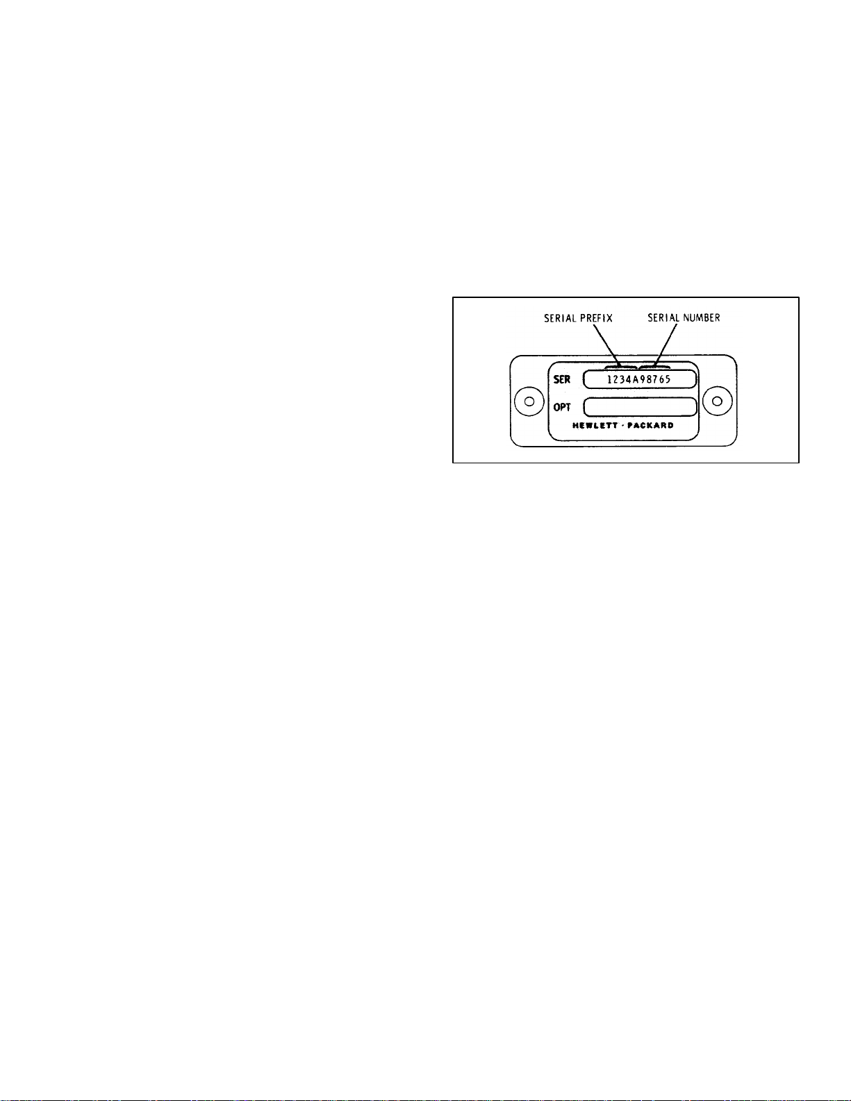
(see Figure 1-2) on the back panel. When the serial
number prefix on the instrument serial number plate of
your instrument is the same as one of the prefix
numbers on the inside title page of this manual, the
manual applies directly to the instrument. When the
instrument serial number prefix is not listed on the inside
title page of this manual, manual change sheets and
manual updating information is provided. Later editions
or revisions to the manual will contain the required
change information in Section VII.
Figure 1-2. Instrument Identification
1-7. DESCRIPTION
1-8. The Hewlett-Packard Model 8556A Spectrum
Analyzer LF Section covers the frequency range from 20
Hz to 300 kHz. When it is combined with an IF Section
and a Display Section it functions as the tuning section
of a low frequency spectrum analyzer.
1-9. The analyzer electronically scans input signals and
displays their frequency and amplitude on a CRT. The
horizontal, x-axis, is calibrated in units of frequency and
the vertical, y-axis, is calibrated in absolute units of
voltage (pV, mV, dBV) or power (dBm). Therefore,
absolute and relative measurements of both amplitude
and frequency can be made.
1-10. The horizontal (frequency) axis can be swept
three different ways:
a. The center of the CRT is set to a frequency
determined by the dial and the analyzer is swept
symmetrically about that frequency.
b. The analyzer is not swept but is used as a fixed
frequency receiver. Signal amplitude can be read on the
CRT and signal modulation can be viewed as with an
oscilloscope.
1-1
Page 13

General Information Model 8556A
c. The analyzer is swept from 0 Hz to a higher
frequency selectable from 200 Hz to 200 kHz.
1-11. The vertical (amplitude) axis provides relative and
absolute measurement capability in volts, dBV, dBm into
600 ohms unbalanced, and dBm into 50 ohms.
1-12. The LF Section's input is isolated from the
instrument chassis so that the CRT display is free of line
frequency spurious responses due to ground loops.
1-13. Accurate frequency calibration is provided by
selecting 20 kHz markers.
1-14. The LF Section also contains a tracking generator
that produces a calibrated signal that precisely tracks the
analyzer tuning frequency. This signal can be used to
test the frequency response of a device; it can also be
used, with a frequency counter, for making frequency
measurements that are accurate to 1 Hz (see Section
III).
1-15. ACCESSORIES SUPPLIED
1-16. The 8556A LF Section requires a special knob on
the IF Section in place of the standard LOG REF LEVEL
control. The special knob has three scales: one is used
for the LF Section log calibration (red scale), one for log
calibration with the RF Sections (black scale), and one
for linear calibration with all units (blue scale). This knob
and an allen wrench to install it are supplied with each
8556A. Extra knobs (HP 08556-00013) are available.
1-17. The 8556A is supplied with the following
accessories: HP 11095A 600 ohm Feed Thru
Termination
HP 11048C 50 ohm Feed Thru Termination
HP 11660A Tracking Generator Shunt (50
ohm output)
1-18. EQUIPMENT REQUIRED BUT NOT SUPPLIED
1-19. The 8556A LF Section must be mated with an IF
Section, such as the 8552A or the 8552B, and a Display
Section, such as the 140T or the 141T, before the units
can perform as a spectrum analyzer.
1-20. IF Sections
greater frequency stability, narrower bandwidths and an
expanded log scale (2 dB per division).
1-22. Display Sections
1-23. The 140T Display Section is equipped with a fixed
persistence, non-storage CRT; the 141T Display Section
is equipped with a variable persistence, storage CRT.
The 143S Display Section has a large screen (8x10
inch) CRT.
1-24. COMPATIBILITY
1-25. The 8556A LF Section is fully compatible with all
current 8552A/B IF Sections; 8552A's with serial prefix
991 and below, and 8552B's with serial prefix 977 and
below must be modified. The modification consists of
adding a white-blue-grey (24 AWG) wire between
8552A/B connectors XA8 pin 8 and J3 pin 40. (See
appropriate 8552 manual for location of connectors.)
NOTE
The 8556A requires a special knob on
the IF Section in place of the
standard LOG REF LEVEL control
(see EQUIPMENT SUPPLIED).
1-26. The 8556A LF Section is fully compatible with all
HP 140S/T, HP 141S/T, and HP 143S Display Sections.
The 8556A can be used with HP 140A/B and 141A/B
Oscilloscope Mainframes but some performance
specifications will be slightly degraded. (For more
information, contact your nearest Hewlett-Packard
office.)
1-27. OPERATING ACCESSORIES
1-28. Operating accessories for use with the
8556A]8552/140 Spectrum Analyzer are listed in Table
1-3. They include a frequency counter, an oscilloscope
camera, and various attenuators and probes.
1-29. TEST EQUIPMENT REQUIRED
1-30. Tables 1-4 and 1-5 list the test equipment and test
equipment accessories required to check, adjust and
repair the 8556A LF Section.
1-21. The 8552A IF Section features calibrated
bandwidths, log and linear amplitude calibration, and
calibrated scan times. The 8552B IF Section has all of
the features of the 8552A and, in addition, manual scan,
1-2
1-31. WARRANTY
1-32. The 8556A LF Section is warranted and certified
as indicated on page C.
Page 14

Model 8556A General Information
Table 1-1. Specifications
8556A/8552B/8552A
FREQUENCY
Range:
20 Hz to 300 kHz - 8552B IF Sec tion
100 Hz to 300 kHz - 8552A IF Section
Tuning Dial Ranges of 0-30 kHz and 0-300 kHz.
Scan Width: (On a 10 div. CRT horizontal axis.)
Per Division: 10 calibrated scan widths from 20 Hz/div
to 20 kHz/div in a 1,2, 5 sequence.
0-10f: 10 calibrated preset scans, from 200 Hz to 200
kHz in a 1, 2, 5 sequence. Analyzer scans from zero
frequency to ten times the scan width per division
setting.
Zero: Analyzer is a fixed tuned receiver.
Accuracy:
Center Frequency: After 1 hour warmup, zero and 300
kHz adjustments, and with the Fine Tune centered,
the dial indicates the display center frequency within
the following specifications:
With 8552B IF Section:
0-30 kHz Range: ±500 Hz
0-300 kHz Range: ±3 kHz
Stability:
Residual FM:
With 8552B IF Section:
Sidebands >60 dB down 50 Hz or more from CW
signal, scan time ≥1 sec/div, 10 Hz band width.
With 8552A IF Section:
Less than 20 Hz peak-to-peak.
Noise Sidebands: More than 90 dB below CW signal,
3 kHz away from signal, with a 100 Hz IF bandwidth.
Frequency Drift: (After 1 hour warmup.)
With 8552B IF Section: Less than 200 Hz/10 min.
With 8552A IF Section: Less than 1 kHz /10 min.
Resolution:
Bandwidth Ranges: IF bandwidths of 10 Hz (50 Hz for
8552A) to 10 kHz are provided in a 1, 3, 10
sequence.
With 8552A IF Section:
0-30 kHz Range: ±1 kHz
0-300 kHz Range: ±5 kHz
Marker: RF markers every 20 kHz accurate to within
±0.01%. Markers controlled by front panel on/off
switch.
Scan Width:
With 8552B IF Section:
Frequency error between any two points on the
display is less than ±3% of the indicated frequency
separation.
With 8552A IF Section:
Frequency error between any two points on the
display is less than ±5% of the indicated frequency
separation.
Bandwidth Accuracy: Individual IF bandwidth 3 dB
points calibrated to ±20% (10 kHz band width ±5%).
Bandwidth Selectivity: 60 dB/3 dB IF bandwidth ratios.
With 8552B IF Section: <11:1 for IF bandwidths from
30 Hz to 3 kHz; <20:1 for 10 kHz IF bandwidth. For
10 Hz bandwidth, 60 dB points are separated by
less than 100 Hz.
With 8552A IF Section: <25:1 for IF bandwidths from
50 Hz to 300 Hz; <20:1 for IF bandwidths from 1 kHz
to 10 kHz.
1-3
Page 15

General Information Model 8556A
Table 1-1. Specifications (cont'd)
AMPLITUDE
Absolute Amplitude Calibration Range:
Log Modes:
dBV 0 dBV = 1 V rms
dBm-600Ω 0 dBm = 1 mW - 600Ω
dBm-502Ω 0 dBm = 1 mW - 502Ω
Input impedance is 1 MΩ. dBm ranges are referenced
with input properly terminated externally.
Log Range: From -150 dBm/dBV to +10 dBm/dBV in
10 dB steps. Log reference level vernier, 0 to -12
dB continuously.
Log Display Range: 10 dB/div on a 70 dB display, or 2
dB/div on a 16 dB display (with 8552B only).
Linear Sensitivity: From 0.1 µV/div to 1V/div in a 1, 2,
10 sequence. Linear sensitivity vernier X1 to X0.25
continuously.
Dynamic Range :
Average Noise Level: Specified with a 600Ω or less
source impedance and INPUT LEVEL at -60
dBm/dBV.
1 kHz IF 10 Hz IF
Mode Bandwidth Bandwidth
dBm-50 Ω <-122 dBm (180 nV) <-142 dBm (18 nV)
dBm-600Ω <-130 dBm (250 nV) <-150 dBm (25 nV)
dBV <-132 dBV (250 nV) <-152 dBV (25 nV)
Linear <400 nV <40 nV
Spurious Responses: Input signal level ≤ INPUT LEVEL
Setting: out of band mixing responses,
TRACKING GENERATOR
harmonic and intermodulation distortion products are
all more than 70 dB below the input signal level 5
kHz to 300 kHz; 60 dB 20 Hz to 5 kHz. Third order
intermodulation products are more than 70 dB below
the input signal level, 5 kHz to 300 kHz with signal
separation >300 Hz.
Residual Reponses: (no signal present at input): with
the INPUT LEVEL at -60 dBm/dBV and the input
terminated with 600Ω or less, all line related residual
responses from 0-500 Hz are below -120 dBm/dBV.
All other residual responses are below -130
dBm/dBV.
Gain Compression: For input signal level 20 dB above
INPUT LEVEL setting gain compression is less than
1 dB.
INPUT LEVEL Control: -10 to -60 dBm/dBV in 10 dB
steps. Accuracy ±0.2 dB. Marking indicates
maximum input levels for 70 dB spurious-free
dynamic range.
Accuracy:
Log Linear
Frequency Response: ±0.2 dB ±2.3%
Switching Between
Bandwidths (at 20°C),
100 Hz to 10 kHz: ±0.5 dB ±5.8%
30 Hz to 10 kHz: ±1.0 dB +12%
10 Hz to 10 kHz: ±1.5 dB ±20%
Display: ±.25 dB/dB ±2.8% of full
but not more 8 div display
than ±1.5 dB
over 70 dB
display range
Frequency Range: Tracks the analyzer tuning, 20 Hz to
300 kHz.
Amplitude Range: Continuously variable from 100 mV
rms to greater than 3V rms into an open circuit.
Amplitude Accuracy: With TRACKING GEN LEVEL in
CAL position, output level at 100 kHz is 100 mV ±0.3
dB into an open circuit.
Frequency Response: ±0.25 dB 50 Hz to 300 kHz.
1-4
Output Impedance: 600Ω.
Spectral Purity:
Residual FM:
With 8552B IF Section: <1 Hz peak-to-peak.
With 8552A IF Section: <20 Hz peak-to-peak.
Harmonic Signals: >40 dB down.
Spurious Outputs: >50 dB down.
Page 16

Model 8556A General Information
Table 1-1. Specifications (cont'd)
INPUT
Input Impedance : 1 MΩ shunted by ≈ 32 pF.
Maximum Input Level: 10V rms, ±200 Vdc.
Ground terminals of BNC input connectors are isolated
from the analyzer chassis ground to minimize ground
loop pickup at low frequencies.
Scan Time: 16 internal scan rates from 0.1 ms/div to 10
sec/div in a 1, 2,5 sequence.
Scan Time Accuracy:
0.1 ms/div to 20 ms/div: ±10%
50 ms/div to 10 sec/div: ±20%.
Power Requirements: 115 or 230 volts ±10%, 50 to 60
Hz, less than 225 watts.
Dimensions:
Model 140T or 141T Display Section: 9-1/5" high
(including height of feet) x 16-3/4" wide x 18-3/8"
deep (229 x 425 x 467 mm).
Model 143S Display Section: 21" high (including height
of feet) x 16-3/4" wide x 18-3/8" deep (533 x 425 x
467 mm).
Maximum Voltage. Isolated Ground to Chassis Ground:
±100 Vdc.
Isolated Ground to Chassis Ground Impedance: 100 kΩ
shunted by approximately 0.3 µf.
GENERAL
Weight:
Model 8556A LF Section: Net. 8 lb (3,7 kg).
Model 8552B IF Section: Net. 9 lb (4,1 kg).
Model 8552A IF Section: Net. 9 lb (4,1 kg).
Model 140T Normal Persistence Display Section: Net
37 lb (16,8 kg).
Model 141T Variable Persistence Display Section:
Net, 40 lb (18 kg).
Model 143S Large Screen Display Section: Net 62 lb
(28,1 kg).
Accessories Included:
Model 11660A Tracking Generator Shunt
Model 11048B 50Ω Feed Thru Termination
Model 11095A 600Ω Feed Thru Termination
1-5
Page 17
General Information Model 8556A
Table 1-2. Supplemental Performance Characteristics
FREQUENCY CHARACTERISTICS
Range: With 300 kHz Center Frequency and 20 kHz/div
Scan Width, analyzer will scan linearly to 400 kHz.
Center Frequency Control: Approximately 10 turns to
cover full dial indicator in both 0-30 kHz and 0-300 kHz
ranges.
Fine Tune: Single turn control, ±50 Hz on 0-30 kHz
range, ±500 Hz on 0-300 kHz range.
Zero Adjust: ±40 kHz range with 8552A, ±12 kHz range
with 8552B.
0-10f Scan Mode: With zero properly adjusted in PER
DIVISION scan, 0 to 10f scan mode will scan from 0
(±500 Hz or 0.2 div, whichever is greater) to ten times
the scan width per division setting. Offset may be
reduced to 0 readjusting frequency zero. Scan
accuracy ±5%.
AMPLITUDE CHARACTERISTICS
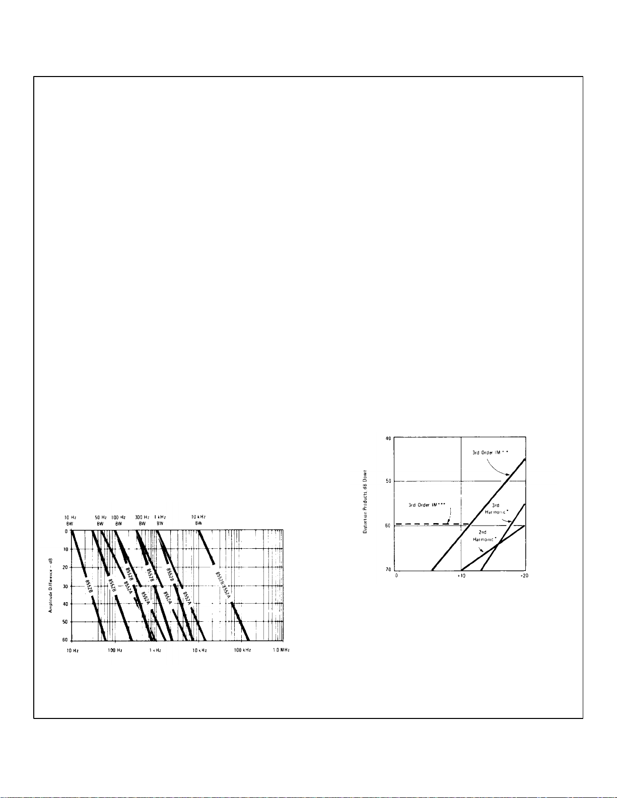
Dynamic Range : For operation from 5 kHz to 300 kHz
with signal levels greater than INPUT LEVEL setting,
see Figure 1-4 for typical distortion.
Accuracy:
Resolution: See Figure 1-3 for curves of typical
8556A/8552B/8552A Spectrum Analyzer resolution
using different IF bandwidths. free dynamic range.
Warmup Drift: (Typical - first hour's operation.)
With 8552B: 500 Hz
With 8552A: 15 kHz
Long Term Drift: (Typical - at fixed center frequency
after one hour warmup.)
With 8552B: 70 Hz/10 min
With 8552A: 400 Hz/10 min
Temperature Drift: (Typical.)
With 8552B: 200 Hz/°C
With 8552A: 2 kHz/°C
Input Level: Provides 50 dB control of input
preamplification and attenuation to prevent input
overload. INPUT LEVEL markings of -60 dBm/dBV to 10 dBm/dBV indicate maximum input level for a
minimum of 70 dB spurious
Log Reference Level: INPUT LEVEL and LOG REF
LEVEL controls provide continuous log reference levels
from +10 dBm/dBV to -80 dBm/dBV (may be decreased
to -92 dBm/dBV by using 12 dB Log Reference Level
Vernier).
Figure 1-3. Typical Spectrum Analyzer
1-6
Signal Level dB Above INPUT LEVEL Setting
* Single input signal, 300 Hz to 300 kHz. Second
and third harmonic distortion products typically 10
dB higher below 30 Hz.
** Two input signals, 5 kHz to 300 kHz with > 300 Hz
signal separation.
*** Two input signals, frequency below 5 kHz with
<300 Hz signal separation.
Figure 1-4. Typical Spectrum Analyzer Distortion
Products
Page 18

Model 8556A General Information
Table 1-2. Supplemental Performance Characteristics (cont'd)
AMPLITUDE CHARACTERISTICS (cont'd)
Accuracy ±0.2 dB (2.3%). Input may be overloaded
up to 20 dB with the analyzer still providing useful
measurement capability. See Figure 1-4.
Log Reference Level Control: Provides 90 dB of IF
gain control in 10 dB steps to cover log and linear
ranges. Accurate to ±0.2 dB (±2.3%).
Log Reference Level Vernier: Provides continuous 12
dB range. Accurate to ±0.1 dB (±1.2%) in 0, -6, -12
dB positions: otherwise ±0.25 dB (±2.8%).
Log Reference Level, switching between 10 dB/div
and 2 dB/div log scales (8552B only):
DISPLAY CHARACTERISTICS
Variable Persistence/Storage (Model 141T):
Plug-ins: Accepts Model 8550 series Spectrum
Analyzer plug-ins and Model 1400 series time
domain plug-ins.
Cathode-ray Tube:
Type: Post-accelerator storage tube, 9000 volt
accelerating potential; aluminized P31 phosphor:
etched safety glass faceplate reduces glare.
Graticule: 8 x 10 division (approximately 7,1 x 8.9 cm)
parallax-free internal graticule: five subdivisions per
major division on horizontal and vertical axes.
Persistence:
Normal: Natural persistence of P31 phosphor
(approximately 0.1 second).
Variable:
Normal Writing Rate Mode: Continuously variable
from less than 0.2 second to more than one
minute (typically to two or three minutes).
Maximum Writing Rate Mode: Typically from 0.2
second to 15 seconds.
Erase: Manual: erasure takes approximately 350 ms;
CRT ready to record immediately after erasure.
Storage Time: Normal writing rate; more than 2 hours at
reduced brightness (typically 4 hours). More than one
minute at maximum brightness.
Accuracy: ±0.6 dB
Temperature Stability: ±0.07 dB/°C.
Amplitude Stability: ±0.07 dB/°C in log. ±0.6 %°C in
linear.
Display Uncalibrated Light: Warns if a combination of
control settings (IF or video bandwidth, scan time or
scan width) degrades absolute calibration for CW
signals. Typically accurate to ±1 position in scan width
or scan time setting.
Video Filter: Averages displayed noise: bandwidth of 10
kHz, 100 Hz and (8552B only) 10 Hz. Bandwidth
accuracy ±20%.
Fast Writing Speed: More than 15 minutes (typically 30
minutes) at reduced brightness or more than 15
seconds at maximum brightness.
Functions Used with Time Domain Plug-ins Only:
Intensity modulation, calibrator, beam finder.
Normal Persistence (Model 140T):
Plug-ins: Same as 141T.
Cathode-ray Tube:
Type: Post-accelerator. 7300 volt potential medium-
short persistence (P7) phosphor, tinted and etched
safety glass face-plate reduces glare. (Normal
persistence of P7 phosphor approximately 3 sec.)
Graticule: 8 x 10 division (approximately 7,6 x 9,5
cm) parallax-free internal graticule: five
subdivisions per major division on horizontal and
vertical axes.
Functions Used with Time Domain Plug-ins Only:
Same as 141T.
Normal Persistence Large Screen Display (Model
143S):
Plug-ins: Same as 141T.
Cathode Ray Tube:
Type: Post-accelerator. 20 kV accelerating
potential aluminized P31 phosphor. (Persistence
approximately 0.1 sec).
Graticule: 8 x 10 divisions (approximately 8 x 10inch) parallax-free internal graticule. five
subdivisions per major division on horizontal and
vertical axes.
Functions Used with Time Domain Plug-ins Only:
Same as 141T.
1-7
Page 19

General Information Model 8556A
Table 1-2. Supplemental Performance Characteristics (cont'd)
GENERAL CHARACTERISTICS
Scan Mode:
Int: Analyzer repetitively scanned by internally
generated ramp; synchronization selected by scan
trigger.
Single: Single scan with reset actuated by front panel
pushbutton.
Ext: Scan determined by 0 to +8 volt external signal;
scan input impedance more than 10 kΩ.
Blanking: -1.5V external blanking signal required.
Manual: Scan determined by front panel control;
continuously variable across CRT in either direction
(8552B only).
Scan Trigger: For Internal Scan Mode, select between:
Auto: Scan free runs.
Line: Scan synchronized with power line frequency.
Ext: Scan synchronized with more than 2 volt (20 volt
max.) trigger signal (polarity selected by internally
located switch in Model 8552 IF Section).
Video: Scan internally synchronized to envelope of RF
input signal (signal amplitude of 1.5 major divisions
peak-to-peak required on display section CRT).
Auxiliary Outputs:
Vertical Output: Approximately 0 to -0.8V for 8 division
deflection on CRT display; approximately 100Ω
output impedance.
Scan Output: Approximately -5 to +5V for 10 div CRT
deflection, 5k Ω output impedance.
Pen Lift Output: 0 to 14V (0V, pen down). Output
available in Int and Single Scan modes and Auto,
Line, and Video Scan Trigger.
CRT Baseline Clipper: Front panel control adjusts
blanking of CRT trace baseline to allow more detailed
analysis of low repetition rate signals and improved
photographic records to be made.
EMI: Conducted and radiated interference is within
requirements of MIL-I-16910C and MIL-I-6181D and
methods CE03 and RE02 of MIL-STD-461 (except 35
to 40 kHz) when 8556A and 8552B are combined in a
140T or 141T Display Section.
1-8
Temperature Range: Operating, 0°C to +55°C,
storage, -40 °C to +75°C.
Page 20

Model 8556A General Information
Table 1-3. Operating Accessories
Model Number Description
HP 10004A 10:1 Divider Probe (oscilloscope type)
HP 1001A Probe to BNC Adapter
HP 1110A Current Probe: Sensitivity: 1 mV/mA
Bandwidth: 1700 Hz (3 dB down)
30 MHz(3 dB down)
Electronic Counter
HP 5381A Frequency Range: 10 Hz to 80 MHz
Sensitivity: 25 mV Input Impedance: 1 Megohm
Gate Time: 0.1, 1 and 10 sec.
Resolution: 1 Hz
Readout: 7 digits
HP 4437A 600 ohm Unbalanced Attenuator
Range: 0-119.9 dB in 0.1 dB increments
Accuracy: ± 0.2 dB to 90 dB
± 0.5 dB to 110 dB
± 1.0 dB to 119.9 dB
Input Power: 1 watt max
HP 197A Oscilloscope Camera
Table 1-4. Test Equipment
Item Minimum Specifications Suggested Use*
Model
AC Voltmeter Voltage Range: 1 mV to 10V full scale (-10 to +2 dB HP 400EL P,A,T
on dB scale)
Frequency Range: 20 Hz to 400 kHz
Accuracy: ± (2.5% of full scale +2.5% of reading)
AC to DC Converter Output: 1V dc for full scale
meter deflection
AC to DC Converter Accuracy: ± (1% of full scale
+1% of reading)
Input Impedance: 10 MΩ shunted by ≈ 25 pF
Oscilloscope Frequency Range: dc to 50 MHz HP 180A/ A, T
AC or DC Coupling 1801A/
Sensitivity: 0.005 V/DIV 1820B
Voltage Accuracy: ±3%
X10 Oscilloscope Probe (2) Division Accuracy: 3%
Resistance: 10 MΩ shunted by 10 pF
*Use: Performance = P: Adjustment = A; Troubleshooting = T
HP 10004A A, T
1-9
Page 21

General Information Model 8556A
Table 1-4. Test Equipment (cont'd)
Item Minimum Specifications Suggested Use*
Model
Frequency Range: 0-60 MHz HP 5327C P, A, T
Counter Sensitivity: 0.1V rms sine wave
Display: 7 digits
Accuracy: ±0.001%
Digital Display: 4 digits HP 3480B, P, A, T
Voltmeter Range: 0 to 100.0 V full scale 3484A
(2 required) 0 to 1000.0 K ohms full scale Opt. 042
for perfor- Accuracy: ± (0.02%7 of reading + 0.05% of range)
mance tests) Polarity: automatic indication
L-C Meter Range: 10 to 40 pF Tektronix A
Accuracy: within 3% of full scale Type 130
Test Oscillator Frequency Range: 20 Hz to 300 kHz HP 651B P, A, T
Dial Accuracy: ±3%
Max Output: > 3.0V into 50 or 600 ohms
Flatness: ± 3%
Distortion: < 1%
Output Monitor: voltmeter monitors output level at
input of attenuator in volts or dB; accurate to ±2%C,
of full scale
Attenuator: range, 90 dB in 10 dB steps
accuracy, ± 0.075 dB, -60 dBm to
+20 dBm
Oscillator Frequency Range: 30 Hz to 100 Hz HP 204D P
Dial Accuracy:± 3%
Max Output: 2.5 V into 600 ohms
Distortion: 0.1% ( 60 dB)
Hum and Noise: <0.01% of output
Filter Set Selectable 500 Hz and 50 kHz Bandpass Filters: White P
> 30 dB of attenuation to second harmonic: Model 2640
> 40 dB of attenuation to third and higher
harmonics
Spectrum HP 8556A/ P
Analyzer 8552B/141T
Only
1-10
*Use: Performance = P: Adjustment A. Troubleshooting = T
Page 22

General Information Model 8556A
Table 1-5. Test Equipment Accessories
Item Minimum Specifications Suggested Use*
Model
BNC Tee One BNC male, two BNC female connectors HP 1250-0781 P
Adapter Selectro Plug to BNC Jack HP 1250-1236 A, T
Adapter Selectro Jack to BNC Jack HP 1250-1237 A, T
Adapter UHF Plug to BNC Jack (UG-273/U) HP 1250-0071 A
Cable Assy Male BNC to Dual Banana Plug, 45 inches long HP 11001A P
Cable Assy Male BNC Connectors, 24 inches long HP 11086A A
Cable Assy Dual Banana Plugs, 44 inches long HP 11000A P
Cable Assy(2) Male BNC Connectors, 48 inches long HP 10503A P, A, T
Cable Assy Dual Banana Plug to Alligator Clips, 5 feet long HP 11002A A, T
Extender 10 Pins, 20 Conductors, for plug-in circuit boards HP 5060-0256 A, T
Board
Screwdrivers Phillips No. 1 A, T
Phillips No. 2 A, T
Pozidriv No. 1 (Stanley No. 5531) HP 8710-0899 A, T
Pozidriv No. 2 (Stanley No. 5332) HP 8710-0900 A, T
Tuning Tool Non-Metallic Shaft (J.F.D. Model No. 5284) HP 8710-1010 A
50-Ohm Supplied with 8556A HP 11048B P, A, T
Feed Thru
Termination
600-Ohm Supplied with 8556A HP 11095A P, A, T
Feed Thru
Termination
Tracking Supplied with 8556A HP 11660A P
Gen Shunt
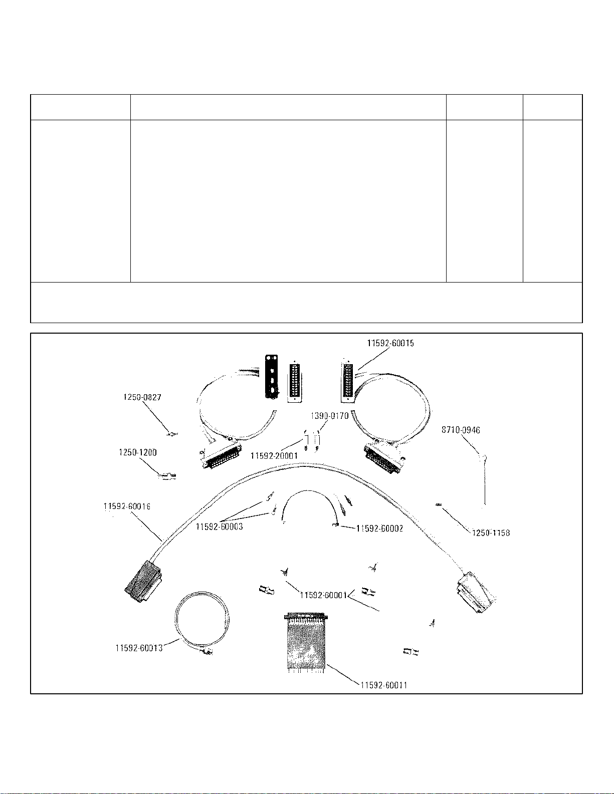
Service Kit Contents: HP 11592A A, T
Display Section to Spectrum Analyzer Extender
Cable Assembly (HP 11592-60015)
Tuning Section to IF Section Interconnection
Cable Assembly (HP 11592-60016)
Selectro Female to BNC Male Test Cable ,3 each,
36 inches long (HP 11592-60001)
Selectro Male to Selectro Female Test Cable,
2 each, 8 inches long (HP 11592-60003)
*Use: Performance = P: Adjustment =A: Troubleshooting = T
1-11
Page 23
General Information Model 8556A
Table 1-5. Test Equipment Accessories (cont'd)
Item Minimum Specifications Suggested Use*
Model
Service Kit Selectro Female to Selectro Female Test Cable, HP 11592A A, T
(cont'd) 2 each, 8 inches long (HP 11592-60002)
Extender Board Assembly, 15 pins, 30 conductors,
for plug-in circuit boards (HP 11592-60011)
Fastener Assembly (2 each: HP 11592-2001 and
HP 1390-0170)
Selectro Jack-to-Jack Adapter (HP 1250-0827)
Wrench, open end, 15/16 inch (HP 8710-0946)
BNC Jack-to-OSM Plug Adapter (HP 1250-1200)
OSM Plug-to-Plug Adapter (HP 1250-1158)
Cable Assembly R and P Connector
(HP 11592-60013)
* Use: Performance = P: Adjustment = A: Troubleshooting = T.
1-12
Figure 1-5. HP 11592A Service Kit
Page 24

Model 8556A Installation
SECTION II
INSTALLATION
2-1. INITIAL INSPECTION
2-2. Mechanical Check
2-3. Check the shipping carton for evidence of damage
immediately after receipt. If there is any visible damage
to the carton, request the carrier's agent be present
when the instrument is unpacked. Inspect the
instrument for physical damage such as bent or broken
parts and dents or scratches. If damage is found refer to
paragraph 2-6 for recommended claim procedures. If
the instrument appears to be undamaged, perform the
electrical check (see paragraph 2-4). The packaging
material should be retained for possible future use.
2-4. Electrical Check
2-5. The electrical check consists of following the
performance test procedures listed in Section IV. These
procedures allow the operator to determine that the
instrument is, or is not, operating within the
specifications listed in Table 1-1. The initial performance
and accuracy of the instrument are certified as stated on
the inside front cover of this manual. If the instrument
does not operate as specified, refer to paragraph 2-6 for
the recommended claim procedure.
2-6.
2-7. DELETED
WARNING
INPUT connector ground is isolated from cabinet
ground. Any voltage present on cable shield will be
present on connector shell (± 100 VDC maximum). If
contacted, this voltage may cause personal injury.
together, electrically connected and inserted in a display
section or oscilloscope mainframe of the 140-series. For
mechanical and electrical connections, refer to Figure
2-1 and paragraph 2-20.
2-12. Power Requirements
2-13. The Spectrum Analyzer can be operated from a
50 to 60 hertz input line that supplies either a 115 volt or
230 volt (±10% in each case) power. Consumed power
varies with the plug-ins used but is normally less than
225 watts. Line power enters the Display Section or
Mainframe, where it is converted to dc voltages, and
then is distributed to the LF and IF Sections via internal
connectors.
2-14. The 115/230 power selector switch at the rear of
the Display Section must be set to agree with the
available line voltage. If the line voltage is 115 volts, the
slide switch must be positioned so that 115 is clearly
visible. The instrument is internally fused for 115 volt
operation, when shipped. If 230 volt source is to be
used, refer to fuse replacement procedures in the
Display Section manual.
2-8.
2-9. PREPARATION FOR USE
CAUTION
Before applying power, check the
rear panel slide switch on the Display
Section for proper position (115 or
230 volts).
2-10. Shipping Configuration
2-11. Because of individual customer requirements,
shipping configurations are flexible. Preparation for use
is based on the premise that the LF and IF Sections are
installed in a Display Section; thus, the Spectrum
Analyzer is physically and functionally complete for use.
Since the LF and IF Sections are usually received
separately, the plug-ins must be mechanically fitted
2-15. Power Cable
2-16. To protect operating personnel, the National
Electrical Manufacturers Association (NEMA) and the
International Electrotechnical Commission (IEC)
recommends that the instrument panel and cabinet be
grounded. The Spectrum Analyzer is equipped with a
three-conductor power cable: the third conductor is the
ground conductor, and when the cable is plugged into an
appropriate receptacle, the instrument is grounded. To
preserve the protection feature when operating the
instrument from a two-contact outlet, use a three-prong
to two-prong adapter and connect the green lead on the
adapter to ground.
2-17. Operating Environment
2-18. The Spectrum Analyzer uses a forced-air cooling
system to maintain required operating temperatures
within the instrument. The air intake and filter are
located on the rear of the Display Section; air is
exhausted through the side panel perforations.
2-1
Page 25

Installation Model 8556A
When operating the instrument, choose a location
which provides at least three inches of clearance around
the rear and both sides. Refer to the Display Section
manual for maintenance instructions for the cooling
system.
2-19. Interconnections
2-20. The LF and IF Sections are normally shipped
separately; the plug-ins must be mechanically fitted
together, electrically connected, and then inserted in the
Display Section or mainframe. To make these
connections, refer to Figure 2-1 and proceed as follows:
a. Set the IF Section on a level bench. Locate slot
near right rear corner of LF Section: also, locate metal
tab on IF Section that engages with this slot.
b. Grasp the 8556A LF Section near middle of
chassis and raise until it is a few inches above the IF
Section.
c. Tilt LF Section until front of assembly is about 2
inches higher than the rear.
d. Engage assemblies in such a way that metal tab
on the rear of the IF Section slips through the slot on LF
Section.
e. With the preceding mechanical interface
completed, gently lower LF Section until electrical plug
and receptacle meet.
a. Push front panel latch in direction of arrow until it
releases.
b. Firmly grasp the middle of latch flange and pull
LF/RF Sections straight out.
c. Locate black press-to-release level near right
front side of LF Section. Press this lever and
simultaneously exert an upward pulling force on front
edge of LF Section.
d. When the two sections separate at the front,
raise LF Section two or three inches and slide metal tab
at rear of IF Section out of the slot in which it is engaged.
2-22. STORAGE AND SHIPMENT
2-23. Original Packaging
2-24. The same containers and materials used in
factory packaging may be used.
2-25. If the instrument is being returned to HewlettPackard for servicing, attach a tag indicating service
required, return address, instrument model number and
full serial number. Mark the container FRAGILE to
assure careful handling.
2-26. In any correspondence refer to the instrument by
model number and full serial number.
2-27. Other Packaging Materials
f. Position LF Section as required to mate the plug
and receptacle. When plug and receptacle are properly
aligned, only a small downward pressure is required to
obtain a snug fit.
g. After the LF and IF Sections are joined
mechanically and electrically, the complete assembly is
ready to insert in the Display Section.
h. Pick up the LF/IF Sections and center in
opening of Display Section. Push forward until assembly
fits snugly into Display Section.
i. Push in front panel latch to securely fasten
assembly in place.
2-21. To separate the LF/IF Sections from Display
Section and to separate the LF Section from the IF
Section, proceed as follows:
2-2
2-28. The following general instructions should be
followed when repackaging with commercially available
materials:
a. Wrap the instrument in heavy paper or plastic.
If shipping to a Hewlett-Packard Service Office or Center
attach a tag indicating the type of service required,
return address, model number and full serial number.)
b. Use a strong shipping container. A double wall
carton made of 350 pound test material is adequate.
c.Use enough shock-absorbing material (three to fourinch layer) around all sides of the instrument to provide
firm cushion and prevent movement inside the container.
Protect the control panel with cardboard.
d. Seal the shipping container securely.
e. Mark the shipping container FRAGILE to assure
careful handling.
Page 26
Model 8556A Installation
Figure 2-1. LF Section and IF Section Interconnections
2-3/2-4
Page 27

Model 8556A Operation
SECTION III
OPERATION
3-1. INTRODUCTION
3-2. This section provides complete operating
instructions for the HP 8556A Spectrum Analyzer LF
Section as used with an 8552 series IF Section and a
140 series Display Section.
3-3. PANEL FEATURES
3-4. Front panel controls, indicators and connectors are
shown and briefly described in Figure 3-1. Rear panel
controls and connectors are shown and described
in Figure 3-2. For a detailed description of IF Section
and Display Section controls and indicators, refer to their
manuals.
3-5. OPERATOR'S CHECKS
3-6. Upon receipt of the analyzer, or when any plug-in is
changed, perform the operational adjustments listed
in Figure 3-2. This procedure corrects for minor
differences between units and ensures that the LF
Section, IF Section and Display Section are properly
matched.
3-7. OPERATING CONSIDERATIONS
3-8. Front panel controls, indicators and connectors are
shown and briefly described in Figure 3-1. The following
information covers general operating considerations.
3-9. RF Input
3-10. The 8556A has an input impedance of 1 Megohm,
shunted by approximately 32 pF, so compensated
oscilloscope probes (see Table 1-3) can be connected
directly to INPUT and used for in-circuit testing. To
compensate an oscilloscope probe for use with the
8556A, use the probe's BNC adaptor to connect the
probe tip to TRACKING GEN OUT. Adjust the probe for
optimum signal flatness on the CRT display.
3-11. Use the feedthrough terminations, 50 ohm and
600 ohm, when the device to be tested must be
terminated in its characteristic impedance (for example,
when measuring dBm). To make a feedthrough
termination for some other impedance, simply connect a
resistor across the analyzer INPUT (connect the resistor
to INPUT ground, not chassis ground). The value of the
resistor should be equal to the characteristic impedance
of the device.
CAUTION
Do not apply more than 10 V rms and
±200 Vdc to INPUT.
3-12. Amplitude Ranges
3-13. The LOG/LINEAR switch on the IF Section works
in conjunction with the dBm/dBV switch on the LF
Section. With LINEAR selected, the analyzer measures
voltage. With LOG selected (either 2 dB or 10 dB on the
8552B), the analyzer measures voltage in dBV (that is,
dB referenced to 1 volt) or power in dBm. The LF
Section is calibrated to measure dBm in 50 or 600 ohms.
3-14. To use 2 dB LOG, first find the signal using 10 dB
LOG; display the desired portion of the signal on the top
16 dB of the CRT display, then switch to 2 dB LOG. The
top of the display, the LOG REF graticule, remains the
same. The -70 dB graticule line becomes -14 dB (each
major division becomes 2 dB).
NOTE
Do not make any VERTICAL GAIN or
POSITION adjustments in 2 dB LOG
as the front panel calibration will
become invalid.
3-15. The LOG REF LEVEL control on the IF Section
has three scales (see EQUIPMENT SUPPLIED in
Section I): the red scale is used for LF Section log
calibration, the black scale is used for RF Section log
calibration, and the blue scale is used for linear
calibration on all units. If the IF Section being used does
not have the red scale, subtract 20 dB from the black
scale to obtain the LOG REF level on the CRT.
3-16. First Mixer Balance
3-17. The first mixer in the 8556A is balanced to insure
a low level of first local oscillator feedthrough appearing
on the display. Excessive LO feedthrough may result in
inaccurate amplitude calibration and excessive
intermodulation distortion. With the dBm/dBV switch set
to 50Ω dBm and INPUT LEVEL set to -60 dBm/dBV, the
first LO feedthrough (zero frequency marker) should be
below -80 dBm. If it is above this level, perform the first
mixer balance adjustment specified below.
3-1
Page 28

Operation Model 8556A
3-18. Remove the top cover from the Display Section
(with power off).
WARNING
Removing the top cover from the
Display Section exposes the operator
to dangerous potentials (up to 7000
volts).
3-19. Set the analyzer controls as follows:
FREQUENCY......................................................0 kHz
BANDWIDTH.......................................................3 kHz
SCAN WIDTH ....................................... PER DIVISION
PER DIVISION.................................................. 10 kHz
INPUT LEVEL ..........................................-60 dBm/dBV
dBm/dBV ....................................................50 Q2 dBm
BASE LINE CLIPPER ............................................ ccw
VIDEO FILTER .................................................. 10 kHz
SCAN TIME PER DIVISION .............5 MILLISECONDS
LOG/LINEAR ..............................................10 dB LOG
LOG REF LEVEL ............................................ -40 dBm
SCAN MODE ..........................................................INT
SCAN TRIGGER ................................................AUTO
POWER ................................................................. ON
NOTE
This procedure assumes that the
analyzer is calibrated as specified in
Figure 3-2 and has been allowed to
warm up at least one-half hour.
3-20. Center the LO feedthrough signal on the display
with the FREQUENCY control.
3-21. Using a non-metallic adjustment tool, alternately
adjust C and R MIXER BALANCE ADJUSTMENTS
(available on the LF Section top cover) to null the LO
feedthrough.
3-22. When the signal is below -80 dBm, turn power off
and replace the top cover.
3-23. OPERATING INSTRUCTIONS
3-24. The following instructions should enable an
operator to make fast, accurate measurements with the
low frequency analyzer. To define each instrument
application is beyond the scope of this manual. For
further details, there is a complete discussion of 8556A
applications in Application Note 134. This application
note is available from your local HP Sales and Service
Office.
3-25. In general, operation of the Spectrum Analyzer
may be accomplished through the following steps:
a. Set the analyzer to scan the appropriate
frequency range with the proper resolution.
b. Adjust the amplitude scale as necessary for the
measurement.
c. Complete the measurement, and interpret the
results.
3-26. Setting the Frequency Scan
3-27. There are three ways to set the frequency scan on
the 8556A. The first is the 0-10f mode of operation.
When this mode is selected, the spectrum analyzer
scans from "zero" frequency to a preset upper limit
selected by the PER DIVISION control. For example, if
the PER DIVISION control is set to 10 kHz, and the 010f mode is selected, the spectrum analyzer will scan
from 0 to 100 kHz, 10 kHz per division. Scans may be
selected from 20 Hz per division to 20 kHz per division in
a 1, 2, 5 sequence.
3-28. The second way to set the frequency scan is the
PER DIVISION mode. In this mode, the frequency scan
is symmetrical about the CENTER FREQUENCY tuned
by the FREQUENCY control. The CENTER
FREQUENCY dial indicates this frequency in two
ranges, 0-30 kHz or 0-300 kHz. The horizontal scale is
then selected by the PER DIVISION setting.
3-29. The third way is the ZERO scan mode. The
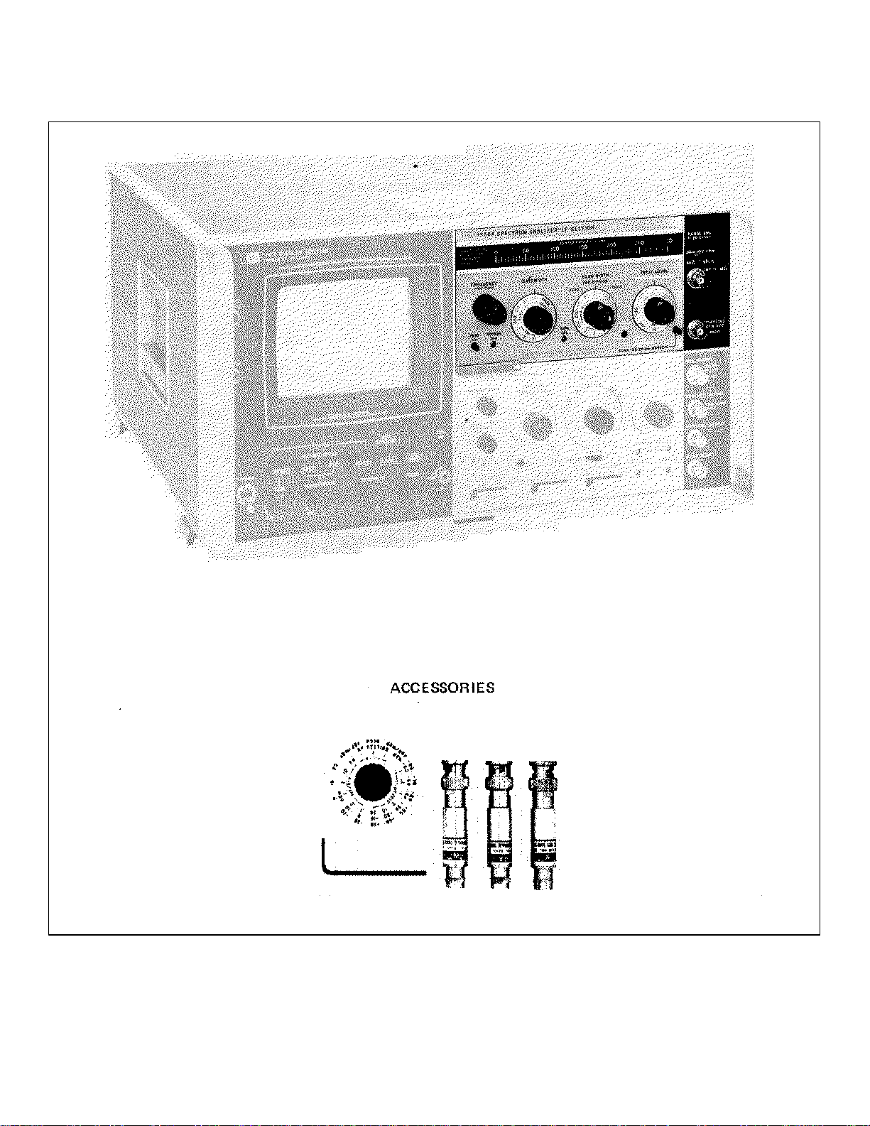
spectrum analyzer becomes a fixed-tuned receiver at the
frequency indicated by the CENTER FREQUENCY dial.
In this mode, amplitude variations are displayed versus
time on the CRT.
3-30. Once the proper frequency scan is chosen, the
resolution needed for the particular measurement should
be determined. Resolution is mainly a function of the IF
bandwidth selected. As narrower IF bandwidths are
used, the resolution increases. At the same time, the
spectrum analyzer must be swept at a slower rate. The
bandwidth used should be only as narrow as is
necessary for the particular application. The best
procedure is to select the bandwidth necessary for the
desired resolution, and then slow the scan rate (SCAN
TIME PER DIVISION) until the DISPLAY UNCAL light is
unlit.
3-31. Adjusting the Amplitude Scale 3-32. Once the
desired signals are displayed on the CRT the amplitude
is set to give an optimum display. The first consideration
is how the amplitude is to be measured. The 8556A can
measure power in dBm (for 50 ohm or 600 ohm
systems), and it can measure voltage on a linear scale
or in dB referred to one volt (dBV) on a log scale.
3-33. If power is the desired parameter, set the
dBm/dBV switch to dBm for the appropriate
3-2
Page 29

Model 8556A Operation
FRONT PANEL FEATURES
(1) DISPLAY UNCAL: warning light indicates that the
CRT display has become uncalibrated due to
incompatible settings of SCAN WIDTH, SCAN
TIME PER DIVISION, BANDWIDTH, and VIDEO
FILTER controls.
(2) FREQUENCY: tunes the CENTER FREQUENCY
in SCAN WIDTH PER DIVISION and ZERO scan
modes. FINE TUNE allows high resolution
adjustments in narrow scans.
(3) ZERO ADJ: calibrates CENTER FREQUENCY
dial for "zero" frequency.
(4) 300 kHz ADJ: calibrates CENTER FREQUENCY
dial for 300 kHz.
(5) BANDWIDTH: selects resolution bandwidth of the
spectrum analyzer from 10 Hz to 10 kHz in a 1, 3
sequence. (8552A, 50 Hz and 100 Hz to 300 kHz
in a 1, 3 sequence.)
(6) AMPL CAL: calibrates display amplitude for
absolute voltage and power measurements.
(7) CENTER FREQUENCY: dial indicates the
CENTER FREQUENCY for SCAN WIDTH PER
DIVISION and ZERO scan modes. Calibrated in 5
kHz increments for 0-300 kHz range and 500 Hz
increments for 0-30 kHz range.
(8) SCAN WIDTH: selects spectrum analyzer
frequency scanning mode. 0-10f repetitively tunes
the spectrum analyzer from "zero" frequency to ten
times the setting of the PER DIVISION control.
(e.g., with PER DIVISION control set at 1 kHz,
scan would be from 0-10 kHz, or 1 kHz per
division.) PER DIVISION mode scans the
spectrum analyzer symmetrically about the
CENTER FREQUENCY with a scan width set by
the PER DIVISION control. In the ZERO scan
mode, the analyzer becomes a fixed frequency
receiver at the CENTER FREQUENCY.
(9) PER DIVISION: selects the CRT horizontal
calibration (frequency scale) in the PER DIVISION
and 0-10f frequency scan modes.
(10) TRACKING ADJ: tunes the TRACKING GEN
OUT frequency to precisely track the tuning
frequency of the spectrum analyzer.
(11) INPUT LEVEL: adjusts the input signal level to
the input mixer and input preamplifier to maximize
dynamic range. This control should be set to
agree with the signal level read on the CRT.
(12) TRACKING GEN LEVEL: adjusts the output level
of the tracking signal present at the TRACKING
GEN OUT. When the CAL position is selected, it
gives an output of 100 mV for calibrating the
spectrum analyzer display. The output can be
increased to 3V.
(13) RANGE kHz : selects CENTER FREQUENCY dial
range of 0-30 kHz or 0-300 kHz.
(14) INPUT: one megohm unbalanced input for signals
to be measured.
(15) dBm/dBV: selects log display absolute calibration
for dB1V or dBm referred to 50 ohms or 600
ohms. For correct dBm measurements, an
external termination of the proper impedance must
be provided for the input signals.
(16) TRACKING GEN OUT: output signal tracks the
spectrum analyzer tuning frequency. The signal
may be used for swept frequency response
measurements or to drive a frequency counter for
accurate frequency measurements. The signal
output also serves to accurately calibrate the
display for absolute amplitude.
(17) kHz MARKERS: places crystal controlled
markers with 20 kHz spacing on CRT. These
markers are accurate to 0.01',, and are useful for
calibrating the frequency axis.
(18) CAL OUTPUT: -30 dBm, 30 MHz signal used for
calibrating amplitude on other tuning sections
(8553B,8554L.8555A).
(19) PEN LIFT OUTPUT, TRIG/BLANK INPUT:
provides -14 V pen lift signal for use with X-Y
recorders during retrace in SINGLE and INT
SCAN MODES with VIDEO. LINE, or AUTO
SCAN TRIGGER. It serves as an input connector
for external blanking signal in the EXT SCAN
MODE. When EXT SCAN TRIGGER is selected,
it becomes an input connector for the external
trigger signal.
(20) VERTICAL OUTPUT: provides output
proportional to vertical deflection on CRT.
Approximately 100 mV per major division with 100
ohm output impedance.
Figure 3-1. Front Panel Features (1 of 4)
3-3
(See foldout, page 3-5, for illustration)
Page 30

Operation Model 8556A
FRONT PANEL FEATURES
(21) SCAN IN/OUT: provides output voltage
proportional to CRT horizontal deflection. 0 volts
equals center screen with 1 volt per division (-5 to
+5V full screen). Output voltage available in
SINGLE, MAN, and INT SCAN MODES. In EXT
SCAN MODE, the connector is used as an input
for 0 to +8V external scan signal.
(22) DISPLAY ADJUST: these controls adjust the
deflection circuit gain and offset levels to match
the IF section to a particular display section.
(23) LOG REF LEVEL LINEAR SENSITIVITY: these
controls set the absolute amplitude calibration of
the CRT display. In the 10 dB LOG or 2 dB LOG
modes, the sum of the two control settings
determines the LOG REF LEVEL (top graticule
line on CRT). In the LINEAR mode, the product of
the two control settings determines the CRT scale
factor in volts per division. A special knob is
provided for use with the 8556A. This knob is
described under OPERATING
CONSIDERATIONS (paragraph 3-15).
(24) LOG/LINEAR: selects display mode for
logarithmic display with scale factors of 10 dB per
division or 2 dB per division or LINEAR display
with scale factor selected by LINEAR
SENSITIVITY (2 dB per division not available with
8552A).
(25) SCAN TRIGGER: selects synchronizing trigger
when in the INT SCAN MODE.
AUTO: scan free runs.
SINGLE: single scan initiated by front panel
pushbutton. SCANNING lamp indicates time
during which analyzer is being scanned.
(27) Initiates or resets scan when SINGLE SCAN
MODE is selected.
(28) SCAN TIME PER DIVISION: selects time
required to scan one major division on CRT
display. Control acts as time base for time domain
operation in ZERO scan.
(29) VIDEO FILTER: post detection low pass filter for
effective averaging of distributed signals such as
noise.
(30) Bandwidths of 10 kHz, 100 Hz, and 10 Hz
selectable; nominal bandwidth 400 kHz in OFF
position. (10 Hz position not available with
8552A.) BASE LINE CLIPPER: allows blanking of
the bright base line area of the CRT for better
photography and improved display of transient
phenomena.
(31) MANUAL SCAN: controls spectrum analyzer
horizontal scan in the MAN SCAN MODE. (Not
available on 8552A.)
(32) CAL 10V and 1V: 10V or 1V square wave used
to calibrate time domain plug-ins ONLY.
LINE: scan synchronized to power line frequency.
EXT.: scan initiated by external positive or
negative pulses (2-20V) applied to TRIG/BLANK
INPUT.
VIDEO: scan internal synchronized to envelope of
RF input signal. Signal amplitude of 1.5 divisions
peak-to-peak (min.) required on display section
CRT.
(26) SCAN MODE: selects scan source.
INT.: analyzer repetitively scanned by internally
generated ramp; synchronization selected by
SCAN TRIGGER. SCANNING lamp indicates
time during which analyzer is being scanned.
EXT.: scan determined by externally applied 0 to
+8V signal at SCAN IN/OUT.
MAN: scan determined by MANUAL SCAN
control; scan continuously variable across CRT in
either direction. (Not available with 8552A.)
Figure 3-1. Front Panel Features (2 of 4)
3-4
(33) FOCUS: focuses CRT spot for best definition.
(34) BEAM FINDER: returns CRT trace to the center
of the screen regardless of deflection potentials
with time domain plug-ins ONLY.
(35) NON STORAGE, CONV: defeats the storage and
variable persistence features of the CRT.
Persistence is that of the standard P31 phosphor.
(36) INTENSITY: adjusts the intensity of the trace on
the CRT.
CAUTION
Excessive INTENSITY will damage
the CRT storage mesh. Whenever
trace blooming occurs, turn
INTENSITY down.
(37) ERASE: erases the CRT in the WRITING SPEED
FAST or STD mode of operation. CRT ready to
record immediately after erasure.
Page 31

Operation
Figure 3-1. Front Panel Features (4 of 4)
3-5
Page 32

Model 8556A
FRONT PANEL FEATURES
(38) PERSISTENCE: adjusts the trace fade rate from
0.1 sec. to more than 2 minutes in the WRITING
SPEED FAST or STD modes of operation.
(39) WRITING SPEED FAST, STD: these controls
select the writing speed of the CRT in the
PERSISTENCE mode of operation. The
WRITING SPEED STD mode is almost always
selected for spectrum analysis applications.
(40) STORE TIME: controls the storage time and
relative brightness of the display in the STORE
mode of operation. Storage time more than 2
minutes at maximum brightness, more than 2
hours at minimum brightness.
(41) STORE: stores the display on the CRT for
extended viewing or photography. The CRT does
not write in the STORE mode.
(42) POWER: controls power to the mainframe and to
both plug-ins.
(43) ASTIG: adjusts the shape of the CRT spot.
(44) TRACE ALIGN : used to adjust the CRT trace to
align with the horizontal graticule lines.
(45) CRT Graticule with LOG and LIN scales. LOG
REF is the level used to reference the amplitude of
displayed signals in the LOG display mode.
LINEAR display amplitude is referenced from the
baseline.
Figure 3-1. Front Panel Features (3 of 4)
Page 33

Operation Model 8556A
OPERATIONAL ADJUSTMENTS
(1) INPUT POWER
a. Set 115/230 switch to correspond with available
input voltage. (The instrument is fused for 115 volt,
50/60 Hz operation; if 230 volt power is used, refer to the
Display Section service manual for fuse replacement
procedures.)
b. Connect line power cord to instrument jack and
to a line power outlet.
(2) INTENSITY MODULATION
Set INT/EXT switch to INT. (Set to EXT only if CRT
Z axis is to be externally modulated normally only
used with 1400 series oscilloscope plug-ins).
(3) FOCUS AND ASTIGMATISM
a. Make the following instrument control settings:
RANGE ..................................................0-300 kHz
FREQUENCY.............................................150 kHz
FINE TUNE .............................................Centered
BANDWIDTH............................................... 10 kHz
SCAN WIDTH.................................. PER DIVISION
PER DIVISION............................................ 20 kHz
INPUT LEVEL ....................................-20 dBm/dBV
dBm/dBV ........................................................ dBV
20 kHz MARKERS ........................................... Out
SCAN TIME PER DIVISION .......5 MILLISECONDS
LOG REF LEVEL ....................................... -10 dBV
Vernier ............................................................ ccw
LOG/LINEAR ........................................10 dB LOG
VIDEO FILTER ...............................................OFF
SCAN MODE ....................................................INT
SCAN TRIGGER ..........................................AUTO
BASE LINE CLIPPER ...................................... ccw
WRITING SPEED ............................................STD
PERSISTENCE ................................................ MIN
INTENSITY ............................................ 12 o'clock
POWER ........................................................... ON
b. Adjust INTENSITY as needed. (Whenever
blooming occurs on CRT, turn INTENSITY down.)
Set LOG REF LEVEL maximum counterclockwise.
Using the VERTICAL POSITION control, bring the
trace to the 50 dB graticule line.
c. Switch the SCAN MODE to MAN, and use the
MANUAL SCAN to bring the CRT dot to the center
of the screen. Adjust FOCUS and ASTIG for the
smallest round dot possible.
(5) HORIZONTAL POSITION AND GAIN
a. Alternately adjust HORIZONTAL GAIN and
HORIZONTAL POSITION so that the trace just fills the
horizontal graticule line.
b. Using the VERTICAL POSITION control, bring
the trace to the bottom graticule line (ignore any slight
misalignment of the trace).
(6) VERTICAL POSITION AND GAIN
a. Connect TRACKING GEN OUT to the INPUT
(do NOT use a feedthrough termination). Set the
TRACKING GEN LEVEL to CAL. Set the VIDEO
FILTER to 10 kHz. Use the LOG REF LEVEL vernier to
set the trace to the -70 dB graticule line at the center of
the CRT. (Adjust AMPL CAL counterclockwise, if
necessary, to lower trace.)
b. Turn the LOG REF LEVEL clockwise 7 steps
(without moving vernier) while observing the trace. The
trace should move up the CRT in 10 dB steps. If it does
not, adjust VERTICAL GAIN to bring the trace to the top
graticule line.
c. Turn the LOG REF LEVEL fully
counterclockwise and repeat steps 6 a. and 6 b. until
no further adjustment is necessary.
(7) AMPLITUDE CALIBRATION
a. Set the LOG REF LEVEL to -20 dBV (set vernier
to zero). Adjust AMPL CAL to bring the trace to the top
graticule line at the center of the screen.
b. Set the LOG/LINEAR switch to LINEAR, and set
LINEAR SENSITIVITY to 20 mV per division. Make any
fine adjustment of the AMPL CAL which is necessary to
bring the trace to the fifth graticule line (5 x 20 mV = 100
mV).
(8) TRACKING ADJUSTMENT
a. Return the LOG/LINEAR switch to 10 dB LOG.
Set the LOG REF LEVEL to -10 dBV, and set the SCAN
WIDTH to ZERO. Reduce the BANDWIDTH to 10 Hz
(50 Hz on 8552A). Adjust TRACK ADJ to bring the trace
as high as possible on the screen.
b. Set the LOG/LINEAR switch to 2 dB LOG (or
LINEAR) and repeat the peaking procedure, then return
to 10 dB LOG.
(4) TRACE ALIGNMENT
Set SCAN MODE to INT. Adjust TRACE ALIGN to
set the trace parallel to the horizontal graticule lines.
Figure 3-2. Operational Adjustments (1 of 3)
3-6
Page 34

Operation
Figure 3-2. Operational Adjustments (3 of 3)
3-7
Page 35

Model 8556A
OPERATIONAL ADJUSTMENTS
(9) FREQUENCY CALIBRATION
a. Disconnect TRACKING GEN OUT from
INPUT and set the controls as follows:
FREQUENCY......................................................0 kHz
RANGE ......................................................... 0-30 kHz
FINE TUNE ....................................................Centered
BANDWIDTH.....................................................300 Hz
SCAN WIDTH ....................................... PER DIVISION
PER DIVISION....................................................1 kHz
20 kHz MARKERS ....................................................In
SCAN TIME PER DIVISION ........... 50 MILLISECONDS
VIDEO FILTER .....................................................OFF
b. Center LO feedthrough signal, at CENTER
FREQUENCY graticule on the display, with ZERO ADJ.
The dial should be accurately set to 0 kHz.
NOTE
If using an 8552A IF Section and
ZERO ADJ will not zero the LO
feedthrough, see paragraph 5-30 in
Section VI.
c. Set RANGE to 0-300 kHz, and slowly tune
FREQUENCY to 300 kHz, counting 20 kHz markers as
they pass the CENTER FREQUENCY graticule on the
display. Center the fifteenth marker (300 kHz) on the
CENTER FREQUENCY graticule.
d. Adjust 300 kHz ADJ so that the dial reads 300
kHz when the fifteenth marker is centered.
e. Repeat steps 9b through 9d until no further
adjustment is necessary.
NOTE
Some minor readjustment of tracking
adjustment and frequency calibration
controls may be necessary from time
to time for narrowband operation.
Figure 3-2. Operational Adjustments (2 of 3)
Page 36

Operation Model 8556A
impedance (600 ohms or 50 ohms). The input should
then be terminated with a feedthrough termination for the
impedance selected.
3-34. For voltage measurements, the dBm/dBV switch
can be set to dBV for a log display, or the LOG/LINEAR
switch can be set to LINEAR for a linear display. If no
feedthrough termination is used, the spectrum analyzer
will display the open circuit voltage. If a feedthrough
termination is used, the voltage displayed will be that
developed across the impedance of the termination.
3-35. The next step is to insure that the spectrum
analyzer is operating linearly. That is, that all spectral
components displayed are present at the input and not
generated in the spectrum analyzer. This is readily
accomplished: read the amplitude of the largest signal
on the CRT, and set the INPUT LEVEL control to the
setting nearest this amplitude. For example, if the
largest signal on the display reads -13 dBV, the INPUT
LEVEL control would be set to -10 dBm/dBV.
3-36. Now set the LOG REF LEVEL or LINEAR
SENSITIVITY controls to give the desired display. One
convenient way to set the LOG REF LEVEL is to set the
-10 dBm/dBV position under the right hand indicator
light. The -60 dBm/dBV position will then fall under the
left hand indicator light. In this position, setting the
INPUT LEVEL control to the amplitude of the largest
signal will bring that signal to the top of the CRT. This
gives the widest possible display dynamic range for
signals between -60 dBm/dBV and -10 dBm/dBV.
3-37. Using the Tracking Generator
3-38. The tracking generator is a flat signal source
whose output frequency precisely, tracks the spectrum
analyzer's tuning frequency. This output can be used as
a source to test devices for frequency response. Also,
by measuring the frequency of the tracking generator's
output with a frequency counter, the frequency of signals
appearing on the spectrum analyzer display can be
precisely determined.
INPUT. Some consideration must be given to the input
and output impedances of the test device. If the device
has a 600 ohm input impedance, the tracking generator
can be connected directly to the device. The 50-ohm
Tracking Generator Shunt supplied with the 8556A
should be used between the tracking generator and the
test device for devices with a 50-ohm input impedance.
3-41. The output of the device should be terminated in
its characteristic impedance. 50 ohm or 600 ohm
devices can be terminated using the feedthrough
terminations, and high impedance devices can be
connected directly to the spectrum analyzer INPUT (see
Figure 3-3). Measure devices which have a different
impedance by using a simple resistive termination.
3-42. The tracking generator output level is 100 mV (-20
dBV) open circuit in the CAL position. This amounts to
50 mV (-26 dBV) across 600 ohms. If the 50 ohm shunt
is used, the output will be 4.17 mV or -34.6 dBm into 50
ohms. The output level increases as TRACKING GEN
LEVEL is turned clockwise from the CAL position.
3-43. System Calibration. The TRACKING GEN OUT
should be connected through any necessary
terminations to the spectrum analyzer INPUT. The
TRACKING GEN LEVEL can then be adjusted to bring
the trace to the top graticule line, thus providing a
convenient reference. The INPUT LEVEL control should
be set to -20 dBm/dBV and the LOG REF LEVEL set to
0 dBm/dBV for maximum measurement range on
passive devices. (Use the dBm scale for 50 ohm
devices and the dBV scale for 600 ohm devices.) 3-44.
Insert the test device in the circuit, and its frequency
response will be displayed directly on the CRT. Insertion
loss can be read directly from the dB scale on the CRT.
3-45. Testing Amplifiers. When measuring amplifier
frequency response, some provision must be made for
the gain of the amplifier to prevent damage to the
spectrum analyzer. A step attenuator should be added
to the test setup to decrease the tracking generator level
by a known amount (see Figure 3-4).
3-39. Frequency Response Measurements. The
frequency scan of the spectrum analyzer is set in much
the same way as described under paragraph 3-26. The
tracking generator's output frequency is determined by
the spectrum analyzer's scan. If a device is being tested
from 0-20 kHz, it is only necessary to set the spectrum
analyzer to scan 0-20 kHz using the 0-10f mode.
3-40. The device under test will be connected in the
signal path between the TRACKING GEN OUT and the
3-8
3-46. Set the attenuator to 0 dB and perform the
calibration procedure described under System
Calibration. Then the attenuation should be increased
by an amount greater than the gain of the amplifier
under test. The gain of the amplifier will be the sum of
the attenuator setting and the dB reading from the CRT
graticule at any point. (Remember, this is a negative
number on the graticule.) For example, the spectrum
analyzer is calibrated for a reference at the top of the
CRT. Now a test
Page 37

Model 8556A Operation
Figure 3-3. Typical Frequency Response Measurement (in 50 Ohms)
Figure 3-4. Typical Amplifier Frequency Response Measurement (in 600 Ohms) Using a Frequency Counter
3-9
Page 38

Operation Model 8556A
amplifier is inserted, and the attenuator is set to 50 dB.
If the amplifier response curve is at the -7 dB graticule
line, the gain is 43 dB (50 dB 7 dB).
3-47. Important Considerations. When using the
tracking generator for swept response measurements,
the spectrum analyzer BANDWIDTH and DISPLAY
UNCAL light take on somewhat different significance.
The BANDWIDTH setting mainly affects the average
noise level and has only a secondary effect on
resolution. Narrowing the BANDWIDTH improves
dynamic range, but requires slower sweep rates. The
DISPLAY UNCAL light in most cases will not apply. The
best procedure in swept response measurements is to
slow the scan rate until the display amplitude remains
constant with changes in SCAN TIME PER DIVISION.
At this point, the scan is the proper rate to satisfy the
requirements of both the spectrum analyzer and the
device under test.
3-48. Spurious responses are not displayed on the CRT
due to the tracking signal source and receiver.
Therefore, measurements may be made over a dynamic
range limited only by gain compression as an upper limit
and system noise as a lower limit.
3-52. Variable Persistence and Storage Functions
3-53. With the 141T Display Section the operator can
set trace persistence for a bright, steady trace that does
not flicker, even on the slow sweeps required for narrow
band analysis. The variable persistence also permits the
display of low repetition rate pulses without flickering
and, using the longest persistence, intermittent signals
can be captured and displayed. The storage capability
allows side-by-side comparison of changing signals.
3-54. Persistence and Intensity. The persistence and
intensity determine how long a written signal will be
visible. Specifically, PERSISTENCE controls the rate at
which a signal is erased and INTENSITY controls the
trace brightness as the signal is written. With a given
PERSISTENCE setting, the actual time of trace visibility
can be increased by greater INTENSITY. Since the
PERSISTENCE control sets the rate of erasing a written
signal, it follows that a brighter trace will require more
time to be erased. Conversely, a display of low intensity
will disappear more rapidly. The same principle applies
to a stored display of high and low intensity.
CAUTION
3-49. Devices, such as filters, which may have
attenuation greater than 100 dB can be measured. The
response can be traced out on the CRT in two 70 dB
segments, and the results can be photographed to give
a composite picture.
3-50. Precise Frequency Measurements. It may be
desired to measure the frequency of a low level signal
which is close to a higher level signal. First, confirm that
TRACK ADJ is correctly adjusted (see Figure 3-2), then
connect a low frequency counter to the tracking
generator's output. Using the MANUAL SCAN mode,
scan the spectrum analyzer until you reach the peak of
the signal response. The frequency displayed on the
counter is the frequency of the signal. Resolution of 1
Hz is possible using narrow scan widths and bandwidths
on the spectrum analyzer. (The counter gate time for
this resolution is 1 second.)
3-51. This same method may be applied to the
measurement of points on a frequency response curve.
Use a high impedance counter and connect it to the
tracking generator's output on a tee with the test device
(see Figure 3-4). Then manually scan to a point of
interest on the response curve and read the frequency.
This method is useful when measuring the 3 dB or 6 dB
bandwidth of a filter, discontinuities in a response
characteristic, or identifying spurious modes on a device.
Excessive INTENSITY will damage
the CRT storage mesh. The
INTENSITY setting for any sweep
speed should just eliminate trace
blooming with minimum
PERSISTENCE setting.
3-55. Storage. The storage controls select the storage
mode in which the CRT functions. In ERASE, STORE
and WRITING SPEED are disconnected and all written
signals are removed from the CRT. The STORE
selector disconnects the WRITING SPEED AND ERASE
functions and implements signal retention at reduced
intensity. In the STORE mode, PERSISTENCE and
INTENSITY have no function.
3-56. Writing Speed. In the FAST mode, the rate of
erasing a written display is decreased. Since the
erasing rate is decreased, the entire screen becomes
illuminated more rapidly and the display is obscured.
The effective persistence and storage time are
considerably reduced.
3-57. Photographic Techniques
3-58. Excellent signal photography is possible when the
Spectrum Analyzer is used with an oscilloscope camera
and when proper techniques are employed. Both the HP
196B and the 197A Oscilloscope Cameras attach
directly to the analyzer's CRT bezel without adapters.
Both cameras also have an Ultra-Violet light source that
causes a
3-10
Page 39

Model 8556A Operation
uniform glow of the CRT phosphor. This gives the
finished photograph a grey background that contrasts
sharply with the white trace and the black graticule lines.
Ultra-Violet illumination is normally used only when the
CRT is of the non-
storage and fixed persistence type (140T Display
Section). For a storage or variable persistence CRT
(141T Display Section), a uniform gray background is
obtained by simply taking the , photograph in STORE
rather than in VIEW.
3-11/3-12
Page 40

Model 8556A Performance Tests
SECTION IV
PERFORMANCE TESTS
4-1. INTRODUCTION
4-2. This section provides instructions for
performance testing the Model 8556A Spectrum
Analyzer LF Section. Front panel checks for routine
inspection are given in Table 4-1. The performance
tests verify that the instrument meets the specifications
listed in Table 1-1.
4-3. Perform the tests in procedural order with the test
equipment called for, or with its equivalent. During the
tests, all circuit boards, shields, covers and attaching
hardware must be in place, and the LF and IF Sections
must be installed in the Display Section. Allow the
analyzer to warm up at least one hour before performing
the tests.
4-4. EQUIPMENT REQUIRED
4-5. Test equipment and test equipment accessories
for the performance tests (designated "P" in the "use"
column) are specified in Tables 1-4 and 1-5. Equipment
other than that listed may be used providing that it meets
or exceeds the minimum specifications listed in the
tables.
4-6. OPERATIONAL ADJUSTMENTS
4-8. FRONT PANEL CHECKS
4-9. The front panel checks provide a quick method for
verifying that the LF Section is operating correctly.
After performing the operational adjustments described
in Figure 3-2, set the analyzer's controls as specified in
Table 4-1 and perform the checks.
4-10. TEST SEQUENCE
4-11. The performance tests are suitable for incoming
inspection, troubleshooting, and preventive
maintenance. A test card for recording data is included
at the back of this section.
4-12. Perform the tests in the following order:
a. Allow analyzer to warm up one hour.
b. Perform operational adjustments listed in Figure
3-2.
c. Perform front panel checks listed in Table 4-1.
d. Perform the performance tests in the order
given.
4-7. Before proceeding to the performance tests,
perform the operational adjustments specified in Figure
3-2 (in Section III). These adjustments correct for minor
differences between units and ensure that the LF
Section, IF Section and Display Section are properly
calibrated.
4-13. Each test is arranged so that the specification
is written as it appears in Table 1-1. Next is a
description of the test that includes any special
instructions. Each test that requires test equipment has
a test setup drawing and a list of required equipment.
4-1
Page 41

Performance Tests Model 8556A
Table 4-1. Front Panel Checks
Function Procedure Result
Calibration 1) Perform operational adjustments specified in 1) Analyzer calibrates
Section III (Figure 3-2), then set analyzer as normally.
follows:
RANGE ........................................................0-300 kHz
FREQUENCY .....................................................0 kHz
BANDWIDTH ....................................................10 kHz
SCAN WIDTH ....................................... PER DIVISION
PER DIVISION ................................................. 20 kHz
INPUT LEVEL ..........................................-30 dBm/dBV
dBm/dBV ......................................................6002 dBm
20 kHz MARKERS ................................................. Out
SCAN TIME PER DIVISION ........... 50 MILLISECONDS
LOG/LINEAR ..............................................10 dB LOG
LOG REF LEVEL ..................................... -20 dBm/dBV
VIDEO FILTER .....................................................OFF
SCAN MODE ..........................................................INT
SCAN TRIGGER ................................................AUTO
BASE LINE 2) Turn BASE LINE CLIPPER full clockwise. 2) At least bottom two
CLIPPER divisions blank on
CRT.
3) Turn BASE LINE CLIPPER full count erclockwise.
Scan 4) Turn SCAN TIME PER DIVISION through its 4) Scan occurs in all
range. positions.
5) Return SCAN TIME PER DIVISION to 50
MILLISECONDS. Center LO feedthrough on
CRT with FREQUENCY.
BANDWIDTH & 6) Reduce SCAN WIDTH PER DIVISION to 20 6) LO feedthrough narrows
SCAN WIDTH Hz, reducing BANDWIDTH to maintain LO as BANDPER DIVISION feedthrough about 2 divisions wide. Reduce WIDTH is reduced
SCAN TIME PER DIVISION to keep DIS- and widens as SCAN
PLAY UNCAL lamp unlit; keep signal centered WIDTH PER DIwith FREQUENCY and FINE TUNE. VISION is reduced.
SCAN WIDTH 7) Set SCAN WIDTH to 0-10f, PER DIVISION 7) LO feedthrough
0-10f to 20 kHz, BANDWIDTH to 1 kHz, and SCAN appears at left
TIME PER DIVISION to 50 MILLISECONDS. graticule on CRT.
8) Depress 20 kHz MARKERS switch. 8) Markers appear at
about every major
DISPLAY UNCAL 9) Increase SCAN TIME PER DIVISION to 20
light MILLISECONDS. 9) DISPLAY UNCAL
light illuminates.
4-2
Page 42

Model 8556A Performance Tests
PERFORMANCE TESTS
4-14. TRACKING GENERATOR AMPLITUDE
SPECIFICATIONS:
Amplitude Range: Continuously variable from 100 mV rms to greater than 3 V rms into an open circuit.
Amplitude Accuracy: With TRACKING GEN LEVEL in CAL position, output level at 100 kHz is 100 Mv ± 0.3 dB into an
open circuit.
Frequency Response: ±0.25 dB, 50 Hz to 300 kHz.
DESCRIPTION: An AC Voltmeter is used to measure the amplitude range and accuracy and the frequency response of
the tracking generator.
EQUIPMENT:
AC Voltmeter ........................................................................................................................HP 400EL
Frequency Counter ............................................................................................................... HP 5327C
24" BNC Cable Assy ............................................................................................................HP 11086A
PROCEDURE:
1. Connect equipment as shown in Figure 4-1, connecting AC Voltmeter directly to TRACKING GEN OUT with 24" BNC
cable.
2. Set analyzer as follows:
RANGE ................................................................................................................................0-300 kHz
FREQUENCY...........................................................................................................................100 kHz
SCAN WIDTH .............................................................................................................................ZERO
TRACKING GEN LEVEL ................................................................................................... CAL 100 mV
Figure 4-1. Tracking Generator Test Setup
3. Set voltmeter to measure 100 mV. It should read 100 mV ±3.5 mV.
Amplitude Accuracy: 96.5 ____103.5 mV
4. Disconnect BNC cable from voltmeter and connect it to Frequency Counter. Set TRACKING GEN LEVEL fully
clockwise, and tune FREQUENCY and FINE TUNE for a 50 Hz reading on counter.
4-3
Page 43

Performance Tests Model 8556A
PERFORMANCE TESTS
4-14. TRACKING GENERATOR AMPLITUDE (cont'd)
5. Set voltmeter to measure 3 volts. Disconnect BNC cable from counter and re-connect it to voltmeter. Voltmeter
should read ≥ 3V:
Amplitude Range: 3V____
6. Reset TRACKING GEN LEVEL to CAL 100 mV, and reset voltmeter to measure 100 mV.
7. Slowly tune FREQUENCY from 50 Hz (set in step 5) to 300 kHz. Voltmeter should indicate a maximum variation of
0.5 dB (±0.25 dB) through entire range:
Frequency Response: _____0.5 dB
4-15. MARKER ACCURACY
SPECIFICATION: RF markers every 20 kHz accurate to within ±0.01%.
DESCRIPTION: The tracking generator is peaked to ensure that it is accurately tracking the analyzer tuning, and a
frequency counter is connected to TRACKING GEN OUTPUT. Marker accuracy is tested using MANUAL SCAN (with
8552B IF Section) or ZERO SCAN (with 8552A IF Section) to tune the analyzer to the markers.
Figure 4-2. Marker Accuracy Test Setup
EQUIPMENT:
Frequency Counter ................................................................................................... HP 5327C
BNC Cable Assembly............................................................................................... HP 10503A
Tuning Tool (or small screwdriver)....................................................................... HP 8710-1010
PROCEDURE:
1. Connect equipment as shown in Figure 4-2, connecting TRACKING GEN OUT to analyzer INPUT with BNC cable.
4-4
Page 44

Model 8556A Performance Tests
PERFORMANCE TESTS
4-15. MARKER ACCURACY (cont'd)
2. Set analyzer as follows:
RANGE .....................................................................................................................0-300 kHz
FREQUENCY...............................................................................................................300 kHz
FINE TUNE ................................................................................................................Centered
BANDWIDTH................................................................................ 10 Hz (8552B) 50 Hz (8552A)
SCAN WIDTH..................................................................................................................ZERO
PER DIVISION................................................................................................................1 kHz
TRACKING GEN LEVEL ......................................................................................... Cal 100 mV
INPUT LEVEL....................................................................................................... -20 dBm/dBV
dBm/dBV........................................................................................................................... dBV
20 kHz MARKERS .............................................................................................................. Out
SCAN TIME PER DIVISION..........................................................................5 MILLISECONDS
LOG REF LEVEL.......................................................................................................... -10 dBV
LOG/LINEAR . .........................................................................................................10 dB LOG
VIDEO FILTER ..................................................................................................................OFF
SCAN MODE .......................................................................................................................INT
SCAN TRIGGER .............................................................................................................AUTO
BASE LINE CLIPPER .........................................................................................................ccw
3. Using tuning tool or small screwdriver, adjust TRACK ADJ to peak trace as high as possible on CRT display.
4. Set LOG/LINEAR to LINEAR and LINEAR SENSITIVITY to 20 mV/DIV and, again, peak trace.
5. Disconnect TRACK ING GEN OUT from analyzer INPUT; connect TRACKING GEN OUT to Frequency Counter (if
necessary, increase TRACKING GEN LEVEL to get reading on counter).
6. Depress 20 kHz MARKERS switch, set BANDWIDTH to 300 Hz, and set SCAN WIDTH to PER DIVISION. Set
LINEAR SENSITIVITY to 2 mV/DIV, SCAN TIMIE PER DIVISION to 50 MILLISECONDS, and center 300 kHz marker
on CRT display with FREQUENCY and FINE TUNE.
7. Set SCAN WIDTH PER DIVISION to 20 Hz, BANDWIDTH to 10 Hz, and SCAN MODE to MAN. Use MANUAL SCAN
knob to set dot on CRT to peak of marker. Frequency Counter should read 300 kHz ±30 Hz:
Marker Accuracy: 299,970 ____ 300,030 Hz
NOTE
With 8552A IF Section, perform test with SCAN WIDTH set to ZERO and
BANDWIDTH set to 50 Hz; peak trace with FINE TUNE to get reading.
8. Set SCAN MODE to INT, and tune FREQUENCY down to next marker (should be at 280 kHz).
9. Set SCAN MODE to MAN and use MANUAL SCAN knob to set dot on CRT to peak of marker. Counter should read
280 kHz ±28 Hz:
Marker Accuracy: 279,972 ____ 280,028 Hz
4-5
Page 45

Performance Tests Model 8556A
PERFORMANCE TESTS
4-16. SCAN WIDTH ACCURACY
SPECIFICATION:
With 8552B IF Section:
Frequency error between any two points on the display is less than +3% of the indicated frequency separation.
With 8552A IF Section:
Frequency error between any two points on the display is less than ±5% of the indicated frequency separation.
DESCRIPTION: Internal 20 kHz markers are used to test scan width accuracy on the CRT display.
PROCEDURE:
1. Set analyzer as follows:
RANGE .................................................................................................................................0-300 kHz
FREQUENCY. ........................................................................................................................100 kHz
FINE TUNE ............................................................................................................................Centered
BANDWIDTH .............................................................................................................................. 1 kHz
SCAN WIDTH ............................................................................................................... PER DIVISION
PER DIVISION ......................................................................................................................... 20 kHz
INPUT LEVEL................................................................................................................... -20 dBm/dBV
dBm/dBV....................................................................................................................................... dBV
20 kHz MARKERS .............................................................................................................................In
SCAN TIME PER DIVISION.................................................................................... 50 MILLISECONDS
LOG REF LEVEL...................................................................................................................... -10 dBV
LOG/LINEAR.......................................................................................................................10 dB LOG
VIDEO FILTER ..............................................................................................................................OFF
SCAN MODE ...................................................................................................................................INT
SCAN TRIGGER .........................................................................................................................AUTO
BASE LINE CLIPPER .....................................................................................................................ccw
2. Note that a 20 kHz marker appears at about every major division on the CRT display. Tune FREQUENCY and FINE
TUNE to center a marker on the -4 graticule line (see Figure 4-3).
3. Measure amount of error, in divisions, that the marker deviates from the +4 graticule line. Marker should appear on
the +4 graticule line plus or minus the specified tolerance (for IF Section being used):
With 8552B IF Section, +0.24 major
divisions: +3.76 ____ ±4.24
With 8552A IF Section, ±0.4 major
divisions: +3.60 ____ +4.40
4. Set BANDWIDTH to 300 Hz, SCAN TIME PER
DIVISION to 0.1 SECONDS, and SCAN WIDTH PER
DIVISION to 5 kHz. Turn FREQUENCY and FINE
TUNE to center a marker on the -4 graticule line.
5. Measure amount of error, in divisions, that the marker
deviates from the +4 graticule line. Marker should
appear on the +4 line plus or minus the specified
tolerance:
Figure 4-3. Scan Width Accuracy Display
4-6
Page 46

Model 8556A Performance Tests
PERFORMANCE TESTS
4-16. SCAN WIDTH ACCURACY (cont'd)
With 8552B IF Section, ±0.24 major divisions: +3.76 ____ +4.24
With 8552A IF Section, ±0.4 major divisions: +3.60 ____ +4.40
NOTE
If 8556A appears to be out of tolerance, re-check scan width accuracy at 160, 220, and 280 kHz. If
8556A scan width accuracy is within tolerance at any frequency, check IF Section scan time
accuracy.
4-17. CENTER FREQUENCY ACCURACY
SPECIFICATION: After 1 hour warmup, zero and 300 kHz adjustments, and with the FINE TUNE centered, the dial
indicates the display center frequency within the following specifications:
With 8552B IF Section:
0-30 kHz Range: ±500 Hz
0-300 kHz Range: ±3 kHz
With 8552A IF Section:
0-30 kHz Range: ±1 kHz
0-300 kHz Range: ± 5 kHz
DESCRIPTION: Dial accuracy is tested using internal 20 kHz markers. Any error between the CENTER FREQUENCY
dial reading and the marker frequency is measured on the CRT display.
PROCEDURE:
1. Set analyzer as follows:
RANGE .................................................................................................................................0-300 kHz
FREQUENCY............................................................................................................................ 20 kHz
FINE TUNE ............................................................................................................................Centered
BANDWIDTH.............................................................................................................................300 Hz
SCAN WIDTH ............................................................................................................... PER DIVISION
PER DIVISION............................................................................................................................... kHz
INPUT LEVEL................................................................................................................... -20 dBm/dBV
dBm/dBV ...................................................................................................................................... dBV
20 kHz MARKERS .............................................................................................................................In
SCAN TIME PER DIVISION.................................................................................... 50 MILLISECONDS
LOG REF LEVEL ..................................................................................................................... -10 dBV
LOG/LINEAR.......................................................................................................................10 dB LOG
VIDEO FILTER ..............................................................................................................................OFF
SCAN MODE. ................................................................................................................................INT
SCAN TRIGGER .........................................................................................................................AUTO
BASE LINE CLIPPER .................................................................................................................... ccw
2. Using FREQUENCY control, center the dial marker on the CENTER FREQUENCY dial every 20 kHz from 20 kHz to
300 kHz (for example, 40 kHz, 60 kHz, 80 kHz, etc.). At each 20 kHz point, a 20 kHz marker should appear at
CENTER FREQUENCY graticule on the CRT within the tolerance shown below:
With 8552B IF Section: -3 ____ +3 divisions
With 8552A IF Section: -5 ____ +5 divisions
4-7
Page 47

Performance Tests Model 8556A
PERFORMANCE TESTS
4-17. CENTER FREQUENCY ACCURACY (cont'd)
3. Switch SCAN WIDTH PER DIVISION to 500 Hz, and switch RANGE to 0-30 kHz. Tune FREQUENCY to 0 kHz and
adjust ZERO ADJ to center LO feedthrough on CENTER FREQUENCY graticule. Then tune FREQUENCY to center
the dial marker on the CENTER FREQUENCY dial at 20 kHz. The 20 kHz marker should appear at CENTER
FREQUENCY graticule on CRT plus or minus the specified tolerance (in major divisions):
With 8552B IF Section: -1 ____ +1 divisions
With 8552A IF Section: -2 ____ +2 divisions
4-18. FREQUENCY RESPONSE
SPECIFICATION: Log: ±0.2 dB; Linear: 2.3%.
DESCRIPTION: The tracking generator's output is calibrated with an AC Voltmeter and used to test the analyzer's
frequency response. The analyzer (with the tracking generator) is set to 20 Hz (if using an 8552B IF Section) or 100 Hz (if
using an 8552A IF Section). The analyzer is then tuned slowly to 300 kHz. Any variations in frequency response are read
on a Digital Voltmeter connected to VERTICAL OUTPUT.
4-8
Figure 4-4. Frequency Response Test Setup
Page 48

Model 8556A Performance Tests
PERFORMANCE TESTS
4-18. FREQUENCY RESPONSE (cont'd)
EQUIPMENT:
AC Voltmeter ........................................................................................................................HP 400EL
Digital Voltmeter (2) ................................................................................. HP 3480B/3484A, Option 042
Frequency Counter ............................................................................................................... HP 5327C
BNC Cable Assy.................................................................................................................. HP 10503A
BNC Tee ....................................................................................................................... HP 1250-0781
Cable Assy.......................................................................................................................... HP 11001A
Cable Assy.......................................................................................................................... HP 11000A
Tracking Gen Shunt ............................................................................................................. HP 11660A
50 Ohm Feed Thru Termination ............................................................................................HP 11048B
24" BNC Cable Assy (2) ...................................................................................................... HP 11086A
Tuning Tool (or small screwdriver)................................................................................... HP 8710-1010
1. Connect equipment as shown in Figure 4-4, connecting TRACKING GEN OUT to analyzer INPUT through the
Tracking Gen Shunt, BNC Tee, 24" BNC Cable Assembly, and the 50 Ohm Feed Thru Termination. Connect AC
Voltmeter to BNC Tee at feed thru with a 24" BNC Cable Assembly; connect first Digital Voltmeter to DC OUTPUT on rear
panel of AC Voltmeter. Connect second Digital Voltmeter to VERTICAL OUTPUT on IF Section.
2. Set analyzer as follows:
RANGE .- .............................................................................................................................. 0-30 kHz
FREQUENCY..............................................................................................................................5 kHz
FINE TUNE ............................................................................................................................Centered
BANDWIDTH .................................................................................................................10 Hz (8552B)
50 Hz (8552A)
SCAN WIDTH..............................................................................................................................ZERO
INPUT LEVEL....................................................................................................................-40 dBm/dBv
TRACKING GEN LEVEL ....................................................................................................... 12 o'clock
20 kHz MARKERS .......................................................................................................................... Out
SCAN TIME PER DIVISION......................................................................................5 MILLISECONDS
LOG/LINEAR............................................................................................................................ LINEAR
LINEAR SENSITIVITY ...........................................................................................................10 mV/DIV
VIDEO FILTER ..........................................................................................................................100 Hz
SCAN MODE ...................................................................................................................................INT
SCAN TRIGGER .........................................................................................................................AUTO
BASE LINE CLIPPER .....................................................................................................................ccw
3. Using tuning tool or small screwdriver, adjust TRACK ADJ to peak trace as high as possible on CRT display.
4. Disconnect Tracking Gen Shunt from TRACKING GEN OUT and connect Frequency Counter to TRACKING GEN
OUT. Set Frequency Counter to measure 100 Hz. Tune FREQUENCY and FINE tune down until counter reads 20
Hz (with 8552B) or 100 Hz (with 8552A). Disconnect counter and re-connect Tracking Gen Shunt to TRACKING GEN
OUT.
5. Set AC Voltmeter to measure 30 mV full scale. Set first Digital Voltmeter (connected to AC Voltmeter) to measure
1.000 volts. Adjust TRACKING GEN LEVEL for a 1.000 V reference on first Digital Voltmeter.
6. Set second Digital Voltmeter (connected to analyzer VERTICAL OUTPUT) to measure 1.000 volts. Adjust LINEAR
SENSITIVITY for a 700.0 mV reference on second Digital Voltmeter.
4-9
Page 49

Performance Tests Model 8556A
PERFORMANCE TESTS
4-18. FREQUENCY RESPONSE (cont'd)
7. Tune FREQUENCY control to frequencies noted below. At each frequency, re-adjust TRACKING GEN LEVEL for a
1.000 volt reading on first Digital Voltmeter, then note reading on second Digital Voltmeter (don't re-adjust LINEAR
SENSITIVITY).
Frequency Reading
1 kHz _____ mV
3 kHz _____ mV
5 kHz _____ mV
10 kHz _____ mV
20 kHz _____ mV
30 kHz _____ mV
Difference between the maximum and minimum readings shall not exceed 32.2 mV.
8. Set RANGE to 0-300 kHz and tune FREQUENCY control to 5 kHz. Again, re-adjust TRACKING GEN LEVEL for a
1.000 volt reading on first Digital Voltmeter. Adjust LINEAR SENSITIVITY for a 700 mV reference on second Digital
Voltmeter.
9. Use instructions in 7 above for frequencies noted below.
Frequency Reading
50 kHz ____ mV
100 kHz ____ mV
150 kHz ____ mV
200 kHz ____ mV
250 kHz ____ mV
300 kHz ____ mV
Difference between the maximum and minimum readings shall not exceed 32.2 mV.
4-19. AVERAGE NOISE LEVEL
SPECIFICATION: Specified with a 600 ohm or less source impedance and INPUT LEVEL at -60 dBm/dBV.
Mode 1 kHz IF Bandwidth 10 Hz IF Bandwidth
dBm - 50 Ω < -122 dBm (180 nV) < -142 dBm (18 nV)
dBm- 600 Ω < -130 dBm (250 nV) < -150 dBm (25 nV)
dBV < -132 dBV (250 nV) < -152 dBV (25 nV)
Linear < 400 nV < 40 nV
DESCRIPTION: Average noise level is observed on the analyzer's calibrated CRT display with no signal input and the
analyzer INPUT terminated in 600 ohms.
NOTE
The 10 Hz bandwidth specification can be checked only when using an 8552B IF Section.
EQUIPMENT:
600 Ohm Feed Thru Termination ................................................................................... HP 11095A
PROCEDURE:
1. Connect 600 Ohm Feed Thru Termination to INPUT. Set the analyzer as follows:
RANGE ..................................................................................................................... 0-30 kHz
FREQUENCY..................................................................................................................7 kHz
FINE TUNE ................................................................................................................Centered
BANDWIDTH...................................................................................................................... kHz
4-10
Page 50

Model 8556A Performance Tests
PERFORMANCE TESTS
4-19. AVERAGE NOISE LEVEL (cont'd)
SCAN WIDTH..............................................................................................................................ZERO
INPUT LEVEL................................................................................................................... -60 dBm/dBV
20 kHz MARKERS .......................................................................................................................... Out
SCAN TIME PER DIVISION.................................................................................... 50 MILLISECONDS
LOG/LINEAR ........................................................................................................................... LINEAR
LINEAR SENSITIVITY ............................................................................................................0.1 V/DIV
Vernier .......................................................................................................................................... ccw
VIDEO FILTER ........................................................................ 10 Hz (with 8552B), 100 Hz (with 8552A)
SCAN MODE ...................................................................................................................................INT
SCAN TRIGGER .........................................................................................................................AUTO
BASE LINE CLIPPER .................................................................................................................... ccw
2. Observe average noise level on CRT display. It should be less than 400 nV (the 4 graticule line on the CRT
represents 400 nV). Tune the analyzer to 300 kHz using FREQUENCY and RANGE controls; the average noise level
should be less than 400 nV throughout the range:
LINEAR noise level: ____ 400 nV
NOTE
Average noise level is read at the mid-point of the noise on the CRT display (see
Figure 4-5).
3. Set LOG/LINEAR to 10 dB LOG. In turn, set dBm/dBV switch to 50 2 dBm, dBV, and 600 Ω dBm; at each setting,
tune the analyzer from 7 kHz to 300 kHz and read the average noise level. It should be as specified below:
50 Ω2 dBm noise level, < -122 dBm: ____ -122 dBm
dBV noise level, <-132 dBV:____ -132 dBV
600 Ω dBm noise level, <-130 dBV: ____ -130 dBV
4. If using an 8552B IF Section, set BANDWIDTH to 10 Hz and check average noise level from 100 Hz to 300 kHz in all
four modes. It should be as specified below:
LINEAR noise level, < 40 nV: ____ 40 nV
50 Ω dBm noise level, <-142 dBm: ____ -142 dBm
dBV noise level, < -152 dBV: ____ -152 dBV
600 Ω dBm noise level, < -150 dBm: ____ -150 dBm
Figure 4-5. Average Noise Level Display
4-11
Page 51

Performance Tests Model 8556A
PERFORMANCE TESTS
4-20. RESIDUAL RESPONSES
SPECIFICATION: (No signal present at INPUT.) With the INPUT LEVEL AT -60 dBm/dBV and the input terminated with
600 ohms or less, all line related residual responses from 0 to 500 Hz are below -120 dBm/dBV. All other residual
responses are below -130 dBm/dBV.
DESCRIPTION: Residual responses are signals that appear on the display with no input signal. To measure them, a
reference is selected so that -120 and -130 dBm/dBV are easily determined, and the display is searched for signals
appearing above this reference.
EQUIPMENT:
50 Ohm Feed Thru Termination HP 11048B
1. Connect 50 Ohm Feed Thru Termination to INPUT and set analyzer as follows:
RANGE ................................................................................................................................. 0-30 kHz
FREQUENCY..............................................................................................................................0 kHz
FINE TUNE ............................................................................................................................Centered
BANDWIDTH.............................................................................................................................100 Hz
SCAN WIDTH................................................................................................................ PER DIVISION
PER DIVISION..........................................................................................................................100 Hz
INPUT LEVEL................................................................................................................... -60 dBm/dBV
dBm/dBV.................................................................................................................................502 dBm
20 kHz MARKERS .......................................................................................................................... Out
SCAN TINIE PER DIVISION .................................................................................... 50 MILLISECONDS
LOG/LINEAR.......................................................................................................................10 dB LOG
LOG REF LEVEL.............................................................................................................. -80 dBm/dBV
Vernier .......................................................................................................................................... ccw
BASE LINE CLIPPER .....................................................................................................................ccw
VIDEO FILTER ..............................................................................................................................OFF
SCAN MODE ..................................................................................................................................INT
SCAN TRIGGER .........................................................................................................................AUTO
NOTE
Instruments that radiate magnetic spurs (such as counters, power supplies, etc.)
should not be operating near 8556A during this test.
2. Using FREQUENCY and FINE TUNE, tune LO feedthrough (0 Hz) to far left graticule line on CRT display (see Figure
4-6).
3. Set BANDWIDTH to 10 Hz (with 8552B IF Section) or 50 Hz (with 8552A IF Section). Set SCAN TIME PER
DIVISION to 2 SECONDS.
4. Measure residual responses from the point that the skirt of the LO feedthrough crosses the -40 dB graticule on the
CRT (-120 dBm) to CENTER FREQUENCY graticule (500 Hz). They should be below -120 dBm:
Line Related Residual Responses: ____ -120 dBm
NOTE
Check that peak of LO feedthrough is below -80 dBm. If it is not, null it (see
Section III) and re-check line related residual responses.
4-12
Page 52

Model 8556A Operation
PERFORMANCE TESTS
4-20. RESIDUAL RESPONSES (cont'd)
5. Check that any residual responses from 500 Hz (CENTER FREQUENCY graticule) to 1 kHz (far right graticule line)
are below -130 dBm:
Residual Responses, 500 Hz to 1 kHz: ____ -130 dBm
6. Set BANDWIDTH to 30 Hz (8552B) or 50 Hz (8552A), SCAN WIDTH PER DIVISION to 2 kHz and SCAN TIME PER
DIVISION to 5 SECONDS. Tune FREQUENCY to 11 kHz. All residual responses should be below -130 dBm:
Residual Responses, 1 kHz to 20 kHz: ____ -130 dBm
7. Set RANGE to 0-300 kHz and tune FREQUENCY to 30 kHz. All residual responses should be below -130 dBm:
Residual Responses, 20 kHz to 40 kHz: ____ -130 dBm
8. Tune FREQUENCY slowly to 300 kHz. All residual responses should be below -130 dBm:
Residual Responses, 40 kHz to 300 kHz: ____ -130 dBm
Figure 4-6. Residual Responses Display
4-13
Page 53

Performance Tests Model 8556A
PERFORMANCE TESTS
4-21. SPURIOUS RESPONSES
SPECIFICATION: Input signal level < INPUT LEVEL setting: out of band mixing responses, harmonic and intermodulation
distortion products are all more than 70 dB below the input signal level 5 kHz to 300 kHz; 60 dB, 20 Hz to 5 kHz. Third
order intermodulation products are more than 70 dB below the input signal level, 5 kHz to 300 kHz with signal separation
> 300 Hz.
DESCRIPTION: An oscillator, with low harmonic distortion, is connected through a bandpass filter, to the analyzer. Any
harmonic distortion due to the analyzer is read on the CRT display. Then intermodulation distortion is checked using a
two-tone test.
Figure 4-7. Spurious Responses Test Setup
EQUIPMENT:
Test Oscillator .........................................................................................................................HP 651B
Oscillator................................................................................................................................HP 204D
BNC Tee ........................................................................................................................HP 1250-0781
BNC Cable Assy ................................................................................................................. HP 10503A
Cable Assy.......................................................................................................................... HP 11000A
Cable Assy.......................................................................................................................... HP 11001A
Filter Set .................................................................................................................. White Model 2640
PROCEDURE:
1. Connect Oscillator through Filter Set to analyzer INPUT as shown in Figure 4-7.
4-14
Page 54

Model 8556A Performance Tests
PERFORMANCE TESTS
4-21. SPURIOUS RESPONSES (cont'd)
2. Set analyzer as follows:
RANGE ......................................................................................................................... 0-300 kHz
FREQUENCY..................................................................................................................... 50 kHz
FINE TUNE .....................................................................................................................Centered
BANDWIDTH......................................................................................................................100 Hz
SCAN WIDTH......................................................................................................... PER DIVISION
PER DIVISION...................................................................................................................500 Hz
INPUT LEVEL........................................................................................................... -10 dBm/dBV
dBm/dBV................................................................................................................................ dBV
20 kHz MARKERS ................................................................................................................... Out
SCAN TIME PER DIVISION.................................................................................... 0.5 SECONDS
LOG/LINEAR................................................................................................................10 dB LOG
LOG REF LEVEL...................................................................................................... -10 dBm/dBV
Vernier .................................................................................................................................. ccw
BASE LINE CLIPPER ............................................................................................................. ccw
VIDEO FILTER ..................................................................................................................100 Hz
SCAN MODE ...........................................................................................................................INT
SCAN TRIGGER .................................................................................................................AUTO
3. Switch Filter Set to 50 kHz filter. Set Oscillator for a 50 kHz, CW signal at -10 dBV. Center signal on analyzer CRT
display with FREQUENCY and FINE TUNE. Set signal peak to CRT LOG REF graticule with Oscillator AMPLITUDE
vernier.
4. Tune FREQUENCY to 100 kHz and 150 kHz; at both frequencies all signals on CRT should be below -70 dB graticule
line.
Harmonic Distortion: -70 dB
5. Switch Filter Set to 500 Hz filter. Set SCAN WIDTH to 0-10f, and set Oscillator for a 500 Hz, CW signal at -10 dBV. If
necessary, set signal peak to CRT LOG REF graticule with Oscillator AMPLITUDE vernier.
6. Set BANDWIDTH to 30 Hz (with 8552B) or 50 Hz (with 8552A ) and set SCAN TIME PER DIVISION to 2 SECONDS.
All harmonics of 500 Hz (1 kHz, 1.5 kHz, etc.) should be below -60 dB graticule line:
Harmonic Distortion: -60 dB
7. Disconnect Filter Set from analyzer INPUT. Connect Test Oscillator and Oscillator to BNC Tee; connect BNC Tee
directly to INPUT.
8. Set one oscillator for a 70 kHz, CW signal (f1), and the other oscillator for a 90 kHz, CW signal (f2). Set both oscillator
output attenuators to -40 dBm.
9. Set INPUT LEVEL to -40 dBV, and SCAN WIDTH PER DIVISION to 20 kHz. Set SCAN TIME PER DIVISION to 2
SECONDS and BANDWIDTH to 300 Hz. Set both oscillator AMPLITUDE verniers so that both signal peaks are 3 dB
below LOG REF graticule on CRT display.
4-15
Page 55

Performance Tests Model 8556A
PERFORMANCE TESTS
4-21. SPURIOUS RESPONSES (cont'd)
10. Refer to Figure 4-8; the signals at 140 kHz (2f1) and 180 kHz (2f2) are oscillator second harmonics. Any second order
intermodulation product (due to the analyzer) will occur at 160 kHz (f1 + f2). Any third order intermodulation products
will occur at 50 kHz (2f1-f2) and at 110 kHz (2f2 f1). The intermodulation products should all be below -70 dB graticule
line:
Intermodulation Products Above 5 kHz:___-70 dB
11. Set one oscillator for a 1.7 kHz, CW signal (f1), and the other oscillator for a 2 kHz, CW signal (f2).
12. Set SCAN WIDTH PER DIVISION knob to 500 Hz, and set BANDWIDTH to 30 Hz (with 8552B IF Section) or 50 Hz
(with 8552A IF Section). If necessary, tune ZERO ADJ until LO feedthrough is centered at far left graticule line.
13. If necessary, use oscillator AMPLITUDE verniers to set both signal peaks 3 dB below LOG REF graticule on CRT.
The signals at 3.4 kHz (2f1) and 4.0 kHz (2f2 ) are oscillator second harmonics. Any second order intermodulation
product will occur at 3.7 kHz (f1 + f2); this will always be centered between the two second harmonics. Any third order
intermodulation product will occur at 1.4 kHz (2f1 f2) and at 2.3 kHz (2f2 f1). The intermodulation products should all be
below -60 dB graticule line:
Intermodulation Products Below 5 kHz:___-60 dB
NOTE
With the 8552A IF Section, the close-in third order intermodulation products will be
hidden in the skirts of the fundamental frequencies.
4-16
Figure 4-8. Intermodulation Distortion Products Display
Page 56

Model 8556A Performance Tests
PERFORMANCE TESTS
4-22. RESIDUAL FM
SPECIFICATION: With 8552B IF Section: Sidebands >60 dB down 50 Hz or more from CW signal, scan time >1 sec/div,
10 Hz bandwidth. With 8552A IF Section: Less than 20 Hz peak-to-peak.
DESCRIPTION: The test is written in two parts: the first part is for the 8552B and tests residual FM by checking a stable,
CW signal for close-in sidebands. The second part is for the 8552A; the signal is slope detected on the linear portion of
the IF filter skirt, then any detected FM is displayed in the time domain.
Figure 4-9. Residual FM Test Setup
EQUIPMENT:
Oscillator ................................................................................................. HP 204D
Cable Assy............................................................................................ HP 11001A
600 Ohm Feed Thru Termination ............................................................ HP 11095A
PROCEDURE:
1. Connect equipment as shown in Figure 4-9, connecting the oscillator to analyzer INPUT through the 600 Ohm Feed
Thru Termination.
2. Set analyzer as follows:
RANGE ............................................................................................................................ 0-30 kHz
FREQUENCY........................................................................................................................2 kHz
FINE TUNE ......................................................................................................................Centered
BANDWIDTH.......................................................................................................................100 Hz
SCAN WIDTH.......................................................................................................... PER DIVISION
PER DIVISION....................................................................................................................500 Hz
INPUT LEVEL............................................................................................................. -20 dBm/dBV
20 kHz MARKERS ................................................................................................................... .Out
dBm/dBV ......................................................................................................................600 O dBm
SCAN TIME PER DIVISION...................................................................................... 0.1 SECONDS
LOG/LINEAR.................................................................................................................10 dB LOG
LOG REF LEVEL........................................................................................................ -20 dBm/dBV
VIDEO FILTER ........................................................................................................................OFF
BASE LINE CLIPPER .............................................................................................................. ccw
SCAN MODE .............................................................................................................................INT
SCAN TRIGGER ...................................................................................................................AUTO
3. Set oscillator for a 2 kHz, CW signal at -20 dBm (read on analzyer CRT). Set NORM/LOW DIST switch on oscillator
rear panel to LOW DIST. If using an 8552B IF Section, proceed to step 4. If using an 8552A IF Section, skip to step
6.
4-17
Page 57

Performance Tests Model 8556A
PERFORMANCE TESTS
4-22. RESIDUAL FM (cont'd)
Figure 4-10. Residual FM Display
4. Center signal on CRT display with FREQUENCY and FINE TUNE. Set BANDWIDTH to 10 Hz, SCAN TIME PER
DIVISION to 2 SECONDS and SCAN WIDTH to 20 Hz. Re-center signal if necessary and set VIDEO FILTER to 10
Hz.
5. All sidebands 2.5 divisions (50 Hz) from CENTER FREQUENCY graticule should be below -60 dB graticule line (see
Figure 4-10):
60 Hz Sidebands (8552B): -60 dB
6. If using an 8552A, set LOG/LINEAR to LINEAR and LINEAR SENSITIVITY to 10 mV/DIV. Center signal on CRT
display with FREQUENCY and FINE TUNE; set SCAN WIDTH PER DIVISION to 200 Hz and BANDWIDTH to 100
Hz.
7. Using LINEAR SENSITIVITY vernier, set signal peak to top horizontal graticule line (see Figure 4-10). Then FINE
TUNE so that upward slope of signal intersects CENTER FREQUENCY graticule line 1 division from the top. Note
where upward slope of signal intersects middle (4) horizontal graticule line.
Horizontal Displacement: divisions
8. Use the horizontal displacement to calculate demodualtion sensitivity:
a. Convert horizontal displacement into hertz. For example, (200 Hz SCAN WIDTH PER DIVISION) x (0.2 div) = 40
Hz.
b. Calculate demodulation sensitivity by dividing the vertical displacement in divisions into horizontal displacement in
Hz. For example, 40 Hz=13.1 Hz
3 div div
9. Turn SCAN WIDTH to ZERO. Tune FREQUENCY and FINE TUNE for a response level within the calibrated three
division range (from 1 division from the top to the center horizontal graticule line).
10. Measure the peak-to-peak deviation and multiply it by the demodulation sensitivity obtained in step 8b above. For
example, 0.5 div p-p signal deviation x 13.3 Hz = 6.65 Hz.
div
Residual FM (8552A): 20 Hz
4-18
Page 58

Model 8556A Performance Tests
PERFORMANCE TESTS
4-23. NOISE SIDEBANDS
SPECIFICATION: More than 90 dB below CW signal, 3 kHz away from signal with a 100 Hz IF bandwidth.
DESCRIPTION: A stable CW signal is applied to the analyzer. The amplitude of the noise sidebands are measured on
the CRT display.
Figure 4-11. Noise Sidebands Test Setup
EQUIPMENT:
Oscillator ............................................................................................................................... HP 204D
Cable Assy. ....................................................................................................................... HP 11001A
600 Ohm Feed Thru Termination . ........................................................................................ HP 11095A
PROCEDURE:
1. Connect equipment as shown in Figure 4-11, connecting the Oscillator to analyzer INPUT through the 600 Ohm Feed
Thru Termination.
2. Set analyzer as follows:
RANGE .................................................................................................................................. 0-30 kHz
FREQUENCY............................................................................................................................ 15 kHz
FINE TUNE ...........................................................................................................................Centered
BANDWIDTH.............................................................................................................................100 Hz
SCAN WIDTH................................................................................................................ PER DIVISION
PER DIVISION............................................................................................................................2 kHz
INPUT LEVEL................................................................................................................... -20 dBm/dBV
20 kHz MARKERS .......................................................................................................................... Out
dBm/dBV .............................................................................................................................600 O dBV
SCAN TIME PER DIVISION............................................................................................ 0.5 SECONDS
LOG/LINEAR.......................................................................................................................10 dB LOG
LOG REF LEVEL................................................................................................................. 0 dBm/dBV
4-19
Page 59

Performance Tests Model 8556A
PERFORMANCE TESTS
4-23. NOISE SIDEBANDS (cont'd)
VIDEO FILTER ..........................................................................................................................OFF
BASE LINE CLIPPER ............................................................................................................... .ccw
SCAN MODE ..............................................................................................................................INT
SCAN TRIGGER ....................................................................................................................AUTO
3. Set Oscillator for a 15 kHz, CW signal at about 0 dBm. Center the signal on analyzer CRT display with FREQUENCY
and FINE TUNE.
4. Set signal peak to LOG REF graticule on CRT with Oscillator AMPLITUDE vernier. Set VIDEO FILTER to 10 Hz (with
8552B IF Section) or 100 Hz (with 8552A IF Section). Set SCAN TIME PER DIVISION to 5 SECONDS.
5. Set LOG REF LEVEL to -20 dBm. Average level of noise sidebands more than 1.5 division (3 kHz) away from signal
should be below -70 dB graticule (-90 dBm).
Noise Sidebands, >90 dB down: -90 dBm
NOTE
Average level of noise sidebands is read at the mid-point of the noise on the CRT
display (see Figure 4-12).
4-20
Figure 4-12. Noise Sidebands Display
Page 60

Model 8556A Performance Tests
PERFORMANCE TESTS
4-24. INPUT LEVEL CONTROL AND GAIN COMPRESSION
SPECIFICATIONS:
INPUT LEVEL Control: -10 to -60 dBm/dBV in 10 dB steps.
Accuracy ±0.2 dB. Marking indicates maximum input levels for 70 dB spurious-free dynamic range. Gain
Compression: For input signal level 20 dB above INPUT LEVEL setting, gain compression is less than 1 dB.
DESCRIPTION: A Test Oscillator's calibrated attenuator is used to test the accuracy of the INPUT LEVEL control. Any
error is read on a Digital Voltmeter connected to the analyzer's VERTICAL OUTPUT. Next, compression is checked by
setting the oscillator 20 dB above the INPUT LEVEL setting.
Figure 4-13. Input Level Control and Gain Compression Test Setup
EQUIPMENT:
Test Oscillator .......................................................................................................................HP 651B
Digital Voltmeter..................................................................................... HP 3480B/3484A, Option 042
BNC Cable Assy................................................................................................................ HP 10503A
50 Ohm Feed Thru Termination .......................................................................................... HP 11048B
Cable Assy........................................................................................................................ HP 11001A
PROCEDURE:
1. Connect equipment as shown in Figure 4-13, connecting the Test Oscillator to INPUT through the 50 Ohm Feed Thru
Termination and the Digital Voltmeter to VERTICAL OUTPUT.
4-21
Page 61

Performance Tests Model 8556A
PERFORMANCE TESTS
4-24. INPUT LEVEL CONTROL AND GAIN COMPRESSION (cont'd)
2. Set analyzer as follows:
RANGE .................................................................................................................................0-300 kHz
FREQUENCY............................................................................................................................ 50 kHz
FINE TUNE ............................................................................................................................Centered
BANDWIDTH............................................................................................................................. 10 kHz
SCAN WIDTH................................................................................................................ PER DIVISION
PER DIVISION............................................................................................................................1 kHz
INPUT LEVEL................................................................................................................... -10 dBm/dBV
20 kHz MARKERS .......................................................................................................................... Out
dBm/dBV............................................................................................................................... 50 O dBm
SCAN TIME PER DIVISION.................................................................................... 20 MILLISECONDS
LOG/LINEAR.......................................................................................................................10 dB LOG
LOG REF LEVEL................................................................................................................. 0 dBm/dBV
Vernier. .......................................................................................................................................... ccw
VIDEO FILTER ..........................................................................................................................100 Hz
BASE LINE CLIPPER .....................................................................................................................ccw
SCAN MODE ..................................................................................................................................INT
SCAN TRIGGER .........................................................................................................................AUTO
3. Set Digital Voltmeter on a range that will measure 700.0 mV. Set Test Oscillator OUTPUT ATTENUATOR to -10
dBm; adjust oscillator frequency to 50 kHz and amplitude controls (COARSE and FINE) for zero on dBm meter scale.
4. Adjust analyzer FREQUENCY and FINE TUNE to peak signal at center of CRT display. Set SCAN WIDTH to ZERO.
Adjust oscillator amplitude controls until Digital Voltmeter reads -700.0 mV.
5. To test INPUT LEVEL control, set INPUT LEVEL and oscillator OUTPUT ATTENUATOR as shown below. In each
case, voltmeter should read -700.0 ±2.0 mV:
INPUT LEVEL/OUTPUT INPUT LEVEL
ATTENUATOR
Settings Error
-10 dBm Reference
-20 dBm -698.0 _____ -702.0 mV
-30 dBm -698.0 _____ -702.0 mV
-40 dBm -698.0_____ -702.0 mV
-50 dBm -698.0 _____ -702.0 mV
-60 dBm -698.0 _____ -702.0 mV
6. To test gain compression, set analyzer INPUT LEVEL and oscillator OUTPUT ATTENUATOR to -10 dBm and adjust
oscillator amplitude controls for zero on dBm meter scale.
7. Set LOG/LINEAR to LINEAR and LINEAR SENSITIVITY to 20 mV/DIV; adjust LINEAR SENSITIVITY vernier for -700
mV read on Digital Voltmeter.
8. Set oscillator OUTPUT ATTENUATOR to +10 dBm; set LINEAR SENSITIVITY to 0.2 V/DIV. Digital Voltmeter should
read -700 ±84 mV:
4-22
-616 -784 mV
Page 62

Model 8556A Performance Tests
PERFORMANCE TESTS
4-25. TRACKING GENERATOR SPECTRAL PURITY
SPECIFICATIONS:
Harmonic Signals: > 40 dB down.
Spurious Outputs: >50 dB down.
NOTE
Testing the analyzer's residual FM also tests the tracking generator's residual FM.
DESCRIPTION: A separate Spectrum Analyzer is used to measure the harmonic and spurious outputs from the 8556A
under test.
Figure 4-14. Tracking Generator Spectral Purity Test Setup
EQUIPMENT:
Spectrum Analyzer. .............................................................................................HP 8556A/8552B/141T
50 Ohm Feed Thru Termination ............................................................................................HP 11048B
BNC Cable Assy.................................................................................................................. HP 10503A
NOTE
If a second spectrum analyzer is not available, an HP 310A Wave Analyzer can be
used to test spectral purity.
PROCEDURE:
1. Connect equipment as shown in Figure 4-14, connecting TRACKING GEN OUT of 8556A under test to INPUT of
separate Spectrum Analyzer; connect through 50 Ohm Feed Thru Termination.
4-23
Page 63

Performance Tests Model 8556A
PERFORMANCE TESTS
4-25. TRACKING GENERATOR SPECTRAL PURITY (cont'd)
2. Set 8556A under test as follows:
RANGE .................................................................................................................................. 0-30 kHz
FREQUENCY............................................................................................................................ 20 kHz
SCAN WIDTH..............................................................................................................................ZERO
TRACKING GEN LEVEL ............................................................................................................ Full cw
3. Set separate Spectrum Analyzer as follows:
RANGE ............................................................................................................................... 0-300 kHz
FREQUENCY.........................................................................................................................200 kHz
FINE TUNE ...........................................................................................................................Centered
BANDWIDTH............................................................................................................................300 Hz
SCAN WIDTH.............................................................................................................................. 0-10f
PER DIVISION......................................................................................................................... 20 kHz
INPUT LEVEL................................................................................................................. -10 dBm/dBV
20 kHz MARKERS ......................................................................................................................... Out
dBm/dBV............................................................................................................................. 50 O dBm
SCAN TIME PER DIVISION.......................................................................................... 0.5 SECONDS
LOG/LINEAR......................................................................................................................10 dB LOG
LOG REF LEVEL..............................................................................................................10 dBm/dBV
VIDEO FILTER ............................................................................................................................OFF
SCAN MODE .................................................................................................................................INT
SCAN TRIGGER .......................................................................................................................AUTO
BASE LINE CLIPPER .................................................................................................................. .ccw
4. Using separate Spectrum Analyzer LOG REF LEVEL vernier, position peak of 20 kHz signal at LOG REF graticule on
CRT. All harmonics of 20 kHz (40 kHz, 60 kHz, 80 kHz, etc.) should be below -40 dB graticule:
Harmonics: -40 dB
5. Switch Spectrum Analyzer SCAN WIDTH to PER DIVISION. All harmonics of 20 kHz should be below -40 dB
graticule:
Harmonics: -40 dB
6. Switch SCAN WIDTH to 0-10f. On 855 6A under test, set TRACKING GEN LEVEL to CAL 100 mV. Disconnect 50
Ohm Feed Thru from Spectrum Analyzer INPUT; connect BNC Cable Assembly directly to INPUT.
7. Set Spectrum Analyzer LOG REF LEVEL to 0 dBm and use vernier to reset peak of 20 kHz signal to LOG REF
graticule on CRT.
8. All spurious signals on CRT (that is, all signals excepting LO feedthrough, 20 kHz, and 20 kHz harmonics) should be
below -50 dB graticule line:
Spurious: -50 dB
9. Switch SCAN WIDTH to PER DIVISION. All spurious signals should be below -50 dB graticule line:
Spurious: -50 dB
4-24
Page 64

Model 8556A Performance Tests
Table 4-2. Performance Test Record (1 of 2)
Hewlett-Packard Model 8556A Test Performed by
Spectrum Analyzer LF Section
Serial No. Date
Para. Test Description Measurement Min. Actual Max.
No. Units
4-14 Tracking Generator Amplitude
Step: 3. Amplitude Accuracy mV 96.5 103.5
5. Amplitude Range V 3
7. Frequency Response dB 0.5
4-15 Marker Accuracy
Step: 7. Marker Accuracy (300 kHz) Hz 299,970 300,030
9. Marker Accuracy (280 kHz) Hz 279,972 280,028
4-16 Scan Width Accuracy
Step: 3. With 8552B (20 kHz/DIV) Divisions +3.76 +4.24
With 8552A (20 kHz/DIV) Divisions +3.60 +4.40
5. With 8552B (5 kHz/DIV) Divisions +3.76 +4.24
With 8552A (5kHz/DIV) Divisions +3.60 +4.40
4-17 Center Frequency Accuracy
Step: 2. With 8552B (0-300 kHz) Divisions -3 +3
With 8552A (0-300 kHz) Divisions -5 +5
3. With 8552B (0-30 kHz) Divisions -1 +1
With 8552A (0-30 kHz) Divisions -2 +2
4-18 Frequency Response
Step: 7. 1 kHz mV 683.9 761.1
3 kHz mV 683.9 761.1
5 kHz mV 683.9 761.1
10 kHz mV 683.9 761.1
20 kHz mV 683.9 761.1
30 kHz mV 683.9 761.1
8. 50 kHz mV 683.9 761.1
100 kHz mV 683.9 761.1
150 kHz mV 683.9 761.1
200 kHz mV 683.9 761.1
250 kHz mV 683.9 761.1
300 kHz mV 683.9 761.1
4-19 Average Noise Level
Step: 2. Linear (1 kHz) nV 400
50 Ω dBm (1 kHz)
dBV (1 kHz) dBV -132
600 Ω dBm (1 kHz)
4. Linear (10 Hz) nV 40
50 Ω dBm (10 Hz)
dBV (10 Hz) dBV -152
600 Ω dBm (10 Hz)
4-20 Residual Responses
Step: 4. Line Related dBm -120
5. 500 Hz to 1 kHz dBm -130
6. 1 kHz to 20 kHz dBm -130
dBm -122
dBm -130
dBm -142
dBm -150
4-25
Page 65

Performance Tests Model 8556A
Table 4-2. Performance Test Record (cont'd)
Para. Test Description Measurement Min Actual Max
No. Units
4-20 Residual Responses (cont'd)
7. 20 kHz to 40 kHz dBm -130
8. 40 kHz to 300 kHz dBm -130
4-21 Spurious Responses
Step 4. Harmonic Distortion (5 kHz to 300 kHz) dB -70
6. Harmonic Distortion (20 Hz to 5 kHz) dB -60
10. Intermod. Products Above 5 kHz dB -70
Intermod. Products Below 5 kHz dB -60
4-22 Residual FM
Step 5. 60 Hz Sidebands (8552B) dB -60
7. Horizontal Displacement Divisions
10. Residual FM (8552A) Hz 20
4-23 Noise Sidebands
Step 5. Noise Sidebands dBm -90
4-24 Input Level Control and Gain Compression
Step 5. INPUT LEVEL: -10 dBm mV -698.0 -702.0
-20 dBm mV -698.0 -702.0
-30 dBm mV -698.0 -702.0
-40 dBm mV -698.0 -702.0
-50 dBm mV -698.0 -702.0
-60 dBm mV -698.0 -702.0
8. Gain Compression mV -616 -784
4-25 Tracking Generator Spectral Purity
Step 4. Harmonics dB -40
5. Harmonics dB -40
8. Spurious dB -50
Spurious dB -50
4-26
Page 66

Model 8556A Adjustments
SECTION V
ADJUSTMENTS
5-1. INTRODUCTION
5-2. This section describes adjustments required to
return the analyzer LF Section to peak operating
condition when repairs are required. Included in this
section are test setups, and check and adjustment
procedures. A test card for recording data is included at
the back of this section. Adjustment location
photographs are contained in foldouts in Section VIII.
5-3. Record data, taken during adjustments, in the
spaces provided or in the data test card at the end of this
section. Comparison of initial data with data taken
during periodic adjustments assists in preventive
maintenance and troubleshooting.
5-4. TEST EQUIPMENT REQUIRED
5-5. Tables 1-4 and 1-5 contain a tabular list of test
equipment and test accessories required in the
adjustment procedures. In addition, the tables contain
the required minimum specifications and a suggested
manufacturers model number.
5-6. In addition to the test equipment and test
accessories in Tables 1-4 and 1-5, a Display Section
and an IF Section are required. Perform the Display
Section and IF Section adjustments prior to performing
the LF Section adjustments.
5-7. Posidriv Screwdrivers
both the LF and IF Sections of the spectrum analyzer.
Some adjustments can be made without this kit by
removing the top cover from both the LF Section and the
Display Section. However, this procedure exposes
dangerous potentials in the Display Section chassis and
should not be used unless absolutely necessary. All
adjustments can and should be performed with the
analyzer plug-ins installed on the extender cables
provided in the service kit.
5-13. Table 1-5, Test Equipment Accessories,
contains a detailed description of the contents of the
service kit, and any item in the kit may be ordered
separately. In the case of the 11592-60015 Extender
Cable Assembly, the wiring is especially critical and
fabrication should not be attempted. However, other
items in the kit may be built if desired.
5-14. Extender Cable Installation
5-15. Push the front panel latch in the direction
indicated by the arrow until the latch disengages and
pops out from the panel. Pull the plug-ins out of the
instrument. Remove the top cover of the LF Section.
5-16. Place the plate end of the HP 11592-60015
Extender Cable Assembly in the Display Section and
press firmly into place so that the plugs make contact.
The plate and plugs cannot be installed upside down as
the plate has two holes corresponding to the two guide
rods in the mainframe.
5-8. Many screws in the instrument appear to be
Phillips, but are not. Table 1-5 gives the name and
number of the Posidriv screwdrivers designed to fit these
screws. To avoid damage to the screw slots, Posidriv
screwdrivers should be used.
5-9. Blade Tuning Tools
5-10. For adjustments requiring a non-metallic metalblade tuning tool, use the J.F.D. Model No. 5284 (HP
8710-1010). In situations not requiring non-metallic
tuning tools, an ordinary small screwdriver or other
suitable tool is sufficient. No matter what tool is used,
never try to force any adjustment control in the analyzer.
This is especially critical when tuning variable slug-tuned
inductors, and variable capacitors.
5-11. HP 11592A Service Kit
5-12. The HP 11592A Service Kit is an accessory item
available from Hewlett-Packard for use in maintaining
5-17. Connect the upper cable plug to the LF Section
and the lower cable plug to the IF Section. The plugs
are keyed so that they will go on correctly and will not
make contact upside down.
5-18. FACTORY SELECTED COMPONENTS
5-19. Table 8-1 contains a list of factory selected
components by reference designation, basis of selection,
and schematic diagram location. Factory selected
components are designated by an asterisk (*) on the
schematic diagrams in Section VIII.
5-20. RELATED ADJUSTMENTS
5-21. These adjustments should be performed when
the troubleshooting information in Section VIII indicates
that an adjustable circuit is not
5-1
Page 67

Adjustments Model 8556A
operating correctly. Perform the adjustments after
repairing, or replacing, the circuit. The troubleshooting
procedures specify the required adjustments.
ADJUSTMENTS
5-23. VOLTAGE CHECKS
REFERENCE: Service Sheet 12 and IF Section and Display Section Operating and Service Manuals.
DESCRIPTION: Dc operating voltages for the LF Section are obtained from the Display Section, the IF Section, and an
isolated power supply in the LF Section. If any of the operating voltages are out of limits, they should be corrected before
performing any of the LF Section adjustments.
5-22. Perform any required Display Section and IF
Section adjustments before performing the LF Section
adjustments. Also, perform the voltage checks in
paragraph 5-23 before performing any of the following
adjustments.
EQUIPMENT:
Digital Voltmeter........................................................................................ HP 3480B/3484A Option 042
Cable Assy ......................................................................................................................... HP 11002A
Extender Cable Assy ...................................................................................................HP 11592-60015
5-2
Figure 5-1. Voltage Checks Test Setup
Page 68

Model 8556A Adjustments
ADJUSTMENTS
5-23. VOLTAGE CHECKS (cont'd)
PROCEDURE:
1. Extend LF and IF Sections on Extender Cable Assembly as shown in Figure 5-1.
2. Connect Digital Voltmeter from -10V test point and +20V test point (located on A7 assembly cover) to chassis ground.
The voltages should be -10 ±0.02V and +20 ±0.10V:
-9.98___-10.02V
+19.90___+20.10V
3. If either voltage is out of limits, see IF Section Operating and Service Manual.
4. Connect voltmeter from -12.6V test point and +100V test point (located at left, rear of Master Board Assembly All) to
chassis ground. The voltages should be -12.6 ±0.2V and +100 ±1.0V:
-12.4___-12.8V
+99.0___+101.0V
5. If either voltage is out of limits, see Display Section Operating and Service Manual.
6. Connect voltmeter from -12.6VF test point (located at left, rear of master board) to chassis ground. (20 kHz
MARKERS button on analyzer front panel should be out.) The voltage should be -11.5 ±0.5V:
-11.0___-12.0V
7. Connect voltmeter from 20 VI test point and -20 VI test point (located on A5 assembly cover) to A5 assembly cover
ground (not chassis ground). The voltages should be +20 ±2V and -20 +2V:
+18 +22V
-18__ -22V
8. If any of the voltages checked in steps 6 and 7 are out of limits, see Service Sheet 12 in this manual.
5-3
Page 69

Adjustments Model 8556A
ADJUSTMENTS
5-24. PRE-ATTENUATOR ADJUSTMENTS: COMP AND C IN
REFERENCE: Service Sheet 4.
DESCRIPTION: Pre-attenuator attenuation is checked. Then its flatness is set, adjusting COMP capacitor A5C7, so that
attenuation at 300 kHz equals attenuation at 3 kHz. C IN capacitor A5C6 is adjusted so that INPUT capacitance does not
change when the attenuator is used.
Figure 5-2. Pre-Attenuator Adjustment Test Setup
EQUIPMENT:
L-C Meter............................................................................................................... Tektronix Type 130
Test Oscillator .......................................................................................................................HP 651B
AC Voltmeter.......................................................................................................................HP 400EL
50 Ohm Feed Thru Termination .......................................................................................... HP 11048B
BNC Cable Assy................................................................................................................ HP 10503A
24" BNC Cable Assy .......................................................................................................... HP 11086A
Adapter .........................................................................................................................HP 1250-1236
Adapter .........................................................................................................................HP 1250-0071
Extender Cable Assy .................................................................................................HP 11592-60015
Tuning Tool ................................................................................................................... HP 8710-1010
PROCEDURE:
1. Connect equipment as shown in Figure 5-2, disconnecting green cable (A3W1) so that AC Voltmeter can be
connected to A5J2 (OUTPUT). Connect Test Oscillator to analyzer INPUT through 50 Ohm Feed Thru Termination.
5-4
Page 70

Model 8556A Adjustments
ADJUSTMENTS
5-24. PRE-ATTENUATOR ADJUSTMENTS: COMP AND C IN (cont'd)
2. Set analyzer as follows (controls not specified do not apply):
dBm/dBV.............................................................................................................................50 Ω dBm
INPUT LEVEL................................................................................................................. -40 dBm/dBV
3. Set Test Oscillator for a 3 kHz -27 dBm signal as follows:
FREQUENCY..................................................................................................................................3.0
RANGE .........................................................................................................................................X 1K
OUTPUT ATTENUATOR .........................................................................................................-20 dBm
AMPLITUDE..............................................................................................................................-7 dBm
4. Set AC Voltmeter to measure -10 dB.
5. Adjust Test Oscillator AMPLITUDE (COARSE and FINE) so that AC Voltmeter reads -10.00 dB.
6. Set analyzer INPUT LEVEL to -30 dBm/dBV. Increase 3 kHz signal from Test Oscillator exactly 30 dB by setting
OUTPUT ATTENUATOR to +10 dBm.
7. The AC Voltmeter should read -10 dB ±0.20 dB:
-9.8 -10.2 dB
8. Set Test Oscillator to 300 kHz by setting RANGE to X100K (don't change oscillator signal amplitude).
9. Adjust COMP capacitor A5C7 until AC Voltmeter reads within ±0.10 dB of reading in step 7 (taken at 3 kHz):
(step 7) ±0.10 dB, 0.10 0.10 dB
10. Disconnect AC Voltmeter, Test Oscillator, and 50 Ohm Feed Thru Termination from analyzer. Don't re-connect green
cable (A3W1) to A5J2 (OUTPUT). Set analyzer dBm/dBV switch to dBV and input level to -40 dBm/dBV.
11. Connect the 24 inch BNC cable assembly to L-C Meter UNKNOWN L or C input, and set meter to measure 32 pF.
Null cable capacitance by zeroing the meter, then connect cable to analyzer INPUT.
12. The L-C Meter should read approximately 32 pF (µµ F):
≈32 pF
13. Set analyzer INPUT LEVEL to -30 dBm/dBV. Adjust C IN capacitor A5C6 until L-C Meter reads within ±0.5 pF of
reading in step 12:
(step 12) ±0.5 pF, 0.5 0.5 pF
14. Disconnect L-C Meter from analyzer INPUT. Re-connect green cable (A3W1) to A5J2 (OUTPUT). Perform mixer
balance adjustments specified in paragraph 5-26.
5-5
Page 71

Adjustments Model 8556A
ADJUSTMENTS
5-25. 50.150 MHz LOCAL OSCILLATOR ADJUSTMENT: A6T1
REFERENCE: Service Sheet 5.
DESCRIPTION: Transformer A6T1 is tuned to peak the signal from the 50.150 MHz local oscillator. Then the signal's
frequency and amplitude are checked.
Figure 5-3. 50.150 MHz Local Oscillator Adjustment Test Setup
EQUIPMENT:
Oscilloscope......................................................................................................HP 180A/1801A/1820B
Frequency Counter ............................................................................................................... HP 5327C
BNC Cable Assy ................................................................................................................. HP 10503A
Adapter. ....................................................................................................................... HP 1250-1236
Extender Cable Assy ...................................................................................................HP 11592-60015
Extender Board............................................................................................................... HP 5060-0256
Tuning Tool ................................................................................................................... HP 8710-1010
PROCEDURE:
1. Connect equipment as shown in Figure 5-3. Remove Frequency Converter Assembly A6 from chassis and re-install
on extender board. Connect Oscilloscope to A6J3 using BNC cable and adapter.
2. Set Oscilloscope to measure 50.150 MHz at about 1V peak-to-peak by setting TIME/DIV to 0.1 µsec and VOLTS/DIV
to 0.2V.
3. Using non-metallic tuning tool, tune transformer A6T1 for maximum signal on Oscilloscope. Signal level should be
0.9V to 1.6V peak-to-peak.
0.9 1.6V P-P
5-6
Page 72

Model 8556A Adjustments
ADJUSTMENTS
5-25. 50.150 MHz LOCAL OSCILLATOR ADJUSTMENT: A6T1 (cont'd)
4. Disconnect BNC cable from Oscilloscope and connect it to Frequency Counter. Set counter to measure 50.150 MHz.
5. Oscillator frequency should be 50.150 MHz ±3.0 kHz:
50.147 50.153 MHz
6. Disconnect BNC cable from A6 assembly; remove extender board and install assembly into chassis. Re-connect
cables to A6J1, J2 and J3. Perform mixer balance adjustments as specified in paragraph 5-26.
5-26. MIXER BALANCE ADJUSTMENTS: C; R and Z
REFERENCE: Service Sheet 5
DESCRIPTION: C, R and Z MIXER BALANCE are adjusted until LO feedthrough measures less than -80 dBm.
Figure 5-4. Mixer Balance Adjustments Test Setup
EQUIPMENT:
Extender Cable Assy ...................................................................................................HP 11592-60015
Tuning Tool ................................................................................................................... HP 8710-1010
50 Ohm Feed Thru Termination ............................................................................................HP 11048B
PROCEDURE:
1. Extend LF and IF Sections on Extender Cable Assembly as shown in Figure 5-4. The A6 assembly should be
mounted in chassis with all screws in place. Connect 50 Ohm Feed Thru Termination to analyzer INPUT.
5-7
Page 73

Adjustments Model 8556A
ADJUSTMENTS
5-26. MIXER BALANCE ADJUSTMENTS: C, R and Z (cont'd)
2. Set analyzer controls as follows:
FREQUENCY..............................................................................................................................0 kHz
BANDWIDTH .............................................................................................................................. 3 kHz
SCANWIDTH................................................................................................................. PER DIVISION
PER DIVISION.......................................................................................................................... 10 kHz
INPUT LEVEL ..................................................................................................................-60 dBm/dBV
dBm/dBV............................................................................................................................... 50 O dBm
BASE LINE CLIPPER .................................................................................................................... ccw
VIDEO FILTER ......................................................................................................................... 10 kHz
SCAN TIME PER DIVISION......................................................................................5 MILLISECONDS
LOG/LINEAR ......................................................................................................................10 dB LOG
LOG REF LEVEL .................................................................................................................... -40 dBm
SCAN MODE ...................................................................................................................................INT
SCAN TRIGGER .........................................................................................................................AUTO
NOTE
This procedure assumes that analyzer has been allowed to warm up at least onehalf hour and that it is calibrated as specified in Section III, Figure 3-2.
3. Center LO feedthrough signal on display with FREQUENCY control.
4. Using non-metallic adjustment tool, adjust C and R MIXER BALANCE (A6R5 and C12) for best null of LO
feedthrough.
5. Adjust Z MIXER BALANCE (A6C22) for LO feedthrough null, then repeat steps 4 and 5 until LO feedthrough is below
-40 dB graticule on display (<-80 dBm):
-80 dBm
6. Secure top cover on 8556A. Repeat step 4 until LO feedthrough is below -40 dB graticule line.
-80 dBm
5-27. TRACKING GENERATOR ADJUSTMENTS: AMPL ADJ and FLATNESS ADJ
REFERENCE: Service Sheet 7
DESCRIPTION: Tracking generator level is adjusted at 100 kHz, flatness is adjusted at 300 kHz, and flatness is checked
across the band from 20 kHz to 300 kHz. Then the generator's ability to deliver power into a load is checked.
NOTE
The following adjustments assume that the analyzer meets its frequency
specifications.
5-8
Page 74

Model 8556A Adjustments
ADJUSTMENTS
5-27. TRACKING GENERATOR ADJUSTMENTS: AMPL ADJ and FLATNESS ADJ (cont'd)
Figure 5-5. Tracking Generator Adjustment Test Setup
EQUIPMENT:
AC Voltmeter .......................................................................................................................HP400EL
600 Ohm Feed Thru Termination ....................................................................................... HP 11095A
24" BNC Cable Assy .......................................................................................................... HP 11086A
Tuning Tool .................................................................................................................. HP 8710-1010
Extender Cable Assy .................................................................................................HP 11592-60015
PROCEDURE:
1. Connect equipment as shown in Figure 5-5, connecting AC Voltmeter directly to TRACKING GEN OUT with 24" BNC
cable.
2. Set analyzer as follows (controls not specified do not apply):
FREQUENCY.........................................................................................................................100 kHz
SCAN WIDTH............................................................................................................................ZERO
RANGE ............................................................................................................................... 0-300 kHz
TRACKING GEN LEVEL ................................................................................................. CAL 100 mV
20 kHz MARKERS ......................................................................................................................... Out
3. Set AC Voltmeter to read 100 mV full scale and adjust AMPL ADJ (A8A1R1) so that voltmeter reads exactly 100 mV
(use non-metallic tuning tool).
4. Set FREQUENCY to 300 kHz and adjust FLATNESS ADJ (A8R9) so that voltmeter reads exactly 100 mV.
5-9
Page 75

Adjustments Model 8556A
ADJUSTMENTS
5-27. TRACKING GENERATOR ADJUSTMENTS: AMPL ADJ and FLATNESS ADJ (cont'd)
5. Slowly tune FREQUENCY from 300 kHz to 20 kHz. The voltmeter should indicate a maximum variation of 5 mV
through entire range:
5 mV
6. Connect 600 Ohm Feed Thru Termination between TRACKING GEN OUT and AC Voltmeter. Set TRACKING GEN
LEVEL full clockwise. Voltmeter should read > 1.5 V:
1.5 V
7. Slowly tune FREQUENCY from 20 kHz to 300 kHz. The voltmeter should indicate a maximum variation of 80 mV
through entire range:
80 mV
5-28. FREQUENCY CALIBRATION ADJUSTMENT: OFFSET ADJ, 300 kHz ADJ, and ZERO ADJ
REFERENCE: Service Sheet 9
DESCRIPTION: OFFSET ADJ is adjusted, and the dial is calibrated with the ZERO ADJ and 300 kHz ADJ controls.
EQUIPMENT
NOTE
This procedure assumes that analyzer horizontal display calibration has been
performed (see Figure 3-2 in Section III).
Figure 5-6. Frequency Calibration Adjustment Test Setup
5-10
Digital Voltmeter...................................................................................... HP 3480B/3484A Option 042
Cable Assy ....................................................................................................................... HP 11002A
Extender Cable Assy .................................................................................................HP 11592-60015
Page 76

Model 8556A Adjustments
ADJUSTMENTS
5-28. FREQUENCY CALIBRATION ADJUSTMENT: OFFSET ADJ, 300 kHz ADJ and ZERO ADJ (cont)
PROCEDURE:
1. Connect equipment as shown in Figure 5-6, connecting Digital Voltmeter between Scan Width Switch Assembly A2,
wafer S2-1R lug 11½ (where white-red-gray. 928, wire is connected) and chassis ground.
2. Set analyzer controls as follows:
FREQUENCY.............................................................................................................................0 kHz
FINE TUNE ...........................................................................................................................Centered
RANGE ............................................................................................................................... 0-300 kHz
BANDWIDTH............................................................................................................................ 10 kHz
SCAN WIDTH............................................................................................................... PER DIVISION
PER DIVISION...........................................................................................................................1 kHz
INPUT LEVEL................................................................................................................. -10 dBm/dBV
BASE LINE CLIPPER ................................................................................................................... ccw
VIDEO FILTER .............................................................................................................................OFF
SCAN TIME PER DIVISION................................................................................... 50 MILLISECONDS
LOG/LINEAR......................................................................................................................10 dB LOG
SCAN MODE .................................................................................................................................INT
SCAN TRIGGER .......................................................................................................................AUTO
3. Center 300 kHz ADJ, and center OFFSET ADJ (A7R13). Center LO feedthrough signal at CENTER FREQUENCY
graticule with ZERO ADJ. Dial should be accurately set to 0 kHz.
4. Adjust OFFSET ADJ for 0.0 ± 5.0 mV read on voltmeter.
5. Set BANDWIDTH to 100 Hz and PER DIVISION to 100 Hz; center signal on display with ZERO ADJ Switch RANGE
to 0-30 kHz; signal shift should be less than 150 Hz:
150 Hz
6. Set BANDWIDTH to 1 kHz, PER DIVISION to 20 kHz and RANGE to 0-300 kHz; push 20 kHz MARKERS switch.
7. Slowly tune FREQUENCY to 300 kHz counting 20 kHz markers as they pass CENTER FREQUENCY graticule on
display. Center fifteenth marker (300 kHz) on CENTER FREQUENCY graticule: adjust 300 kHz ADJ so that dial
reads 300 kHz when fifteenth marker (300 kHz) is centered.
8. Tune FREQUENCY to 0 kHz. Adjust ZERO ADJ to center LO feedthrough (0 Hz) on display.
9. Repeat steps 7 and 8 until no further adjustment is necessary.
5-29. ANALOGIC CHECKS
REFERENCE: Service Sheet 10 and IF Section Operating and Service Manual.
DESCRIPTION: Perform the display calibration check tabulated below. If an adjustment is required, refer to the analogic
adjustment procedure in the IF Section manual.
If the table indicates that the DISPLAY UNCAL light should be off, it is acceptable for the light to be on if the light
subsequently goes off when either SCAN TIME PER DIVISION or SCAN WIDTH PER DIVISION is switched one position
counter-clockwise.
5-11
Page 77

Adjustments Model 8556A
ADJUSTMENTS
5-29. ANALOGIC CHECKS (cont'd)
Table 5-1. Analogic Display Calibration Check
VIDEO FILTER
10 Hz 2 SECONDS 100 Hz 1 kHz PER DIVISION OFF
10 Hz 1 SECOND 100 Hz 1 kHz PER DIVISION ON
100 Hz 0.2 SECONDS 1 kHz 10 kHz PER DIVISION OFF
100 Hz 0.1 SECONDS 1 kHz 10 kHz PER DIVISION ON
10 kHz 10 MILLISECONDS 3 kHz 20 kHz PER DIVISION OFF
10 kHz 5 MILLISECONDS 3 kHz 20 kHz PER DIVISION ON
OFF 5 MILLISECONDS 3 kHz 20 kHz ZERO OFF*
OFF 2 MILLISECONDS 10 kHz 20 kHz PER DIVISION OFF
OFF 5 MILLISECONDS 3 kHz 20 kHz PER DIVISION OFF
OFF 5 MILLISECONDS 1 kHz 20 kHz PER DIVISION ON
OFF 20 MILLISECONDS 1 kHz 10 kHz PER DIVISION OFF
OFF 20 MILLISECONDS 300 Hz 10 kHz PER DIVISION ON
OFF 50 MILLISECONDS 300 Hz 2 kHz PER DIVISION OFF
OFF 50 MILLISECONDS 100 Hz 2 kHz PER DIVISION ON
OFF 0.1 SECONDS 100 Hz 500 Hz PER DIVISION OFF
OFF 0.1 SECONDS 30 Hz 500 Hz PER DIVISION ON
OFF 0.2 SECONDS 30 Hz 100 Hz PER DIVISION OFF
OFF 0.2 SECONDS 10 Hz 100 Hz PER DIVISION ON
OFF 0.5 SECONDS 10 Hz 20 Hz PER DIVISION OFF
OFF 0.5 SECONDS 300 Hz 20 Hz PER DIVISION OFF
SCAN TIME
PER DIVISION
BAND-
WIDTH
SCAN WIDTH
PER DIVISION
SCAN WIDTH
DISPLAY
UNCAL
LIGHT
OFF 0.2 SECONDS 300 Hz 20 kHz PER DIVISION ON
OFF 0.2 SECONDS 300 Hz 10 kHz PER DIVISION OFF
OFF 0.1 SECONDS 300 Hz 10 kHz PER DIVISION ON
OFF 0.1 SECONDS 300 Hz 5 kHz PER DIVISION OFF
OFF 50 MILLISECONDS 300 Hz 5 kHz PER DIVISION ON
OFF 50 MILLISECONDS 300 Hz 2 kHz PER DIVISION OFF
OFF 20 MILLISECONDS 300 Hz 2 kHz PER DIVISION ON
OFF 20 MILLISECONDS 300 Hz 1 kHz PER DIVISION OFF
OFF 10 MILLISECONDS 300 Hz 1 kHz PER DIVISION ON
OFF 10 MILLISECONDS 300 Hz 500 Hz PER DIVISION OFF
OFF 5 MILLISECONDS 300 Hz 500 Hz PER DIVISION ON
OFF 5 MILLISECONDS 300 Hz 200 Hz PER DIVISION OFF
OFF 2 MILLISECONDS 300 Hz 200 Hz PER DIVISION ON
OFF 2 MILLISECONDS 300 Hz 100 Hz PER DIVISION OFF
OFF 1 MILLISECOND 300 Hz 100 Hz PER DIVISION ON
OFF 1 MILLISECOND 300 Hz 50 Hz PER DIVISION OFF
* No exception allowed
5-12
Page 78

Model 8556A Adjustments
ADJUSTMENTS
5-30. 8552A 47 MHz LO ADJUSTMENT
REFERENCE: Service Sheet 9 and 8552A IF Section Operating and Service Manual.
DESCRIPTION: On some HP Model 8552A Spectrum Analyzer IF Sections, long term aging may have caused the center
frequency of the 47 MHz LO to drift beyond the zero adjustment range of the 8556A. If this is the case, the following
simplified 47 MHz LO adjustment procedure can be used to readjust center frequency and tuning accuracy.
EQUIPMENT:
Extender Cable Assy (if not available, see step 1)..................................................................................HP 11592-60015
Tuning Tool ................................................................................................................................................. 8710-1010
PROCEDURE:
1. Extend LF and IF Sections on Extender Cable Assembly (see paragraph 5-15 for step-by-step procedure). If the
Extender Cable Assembly is not available, the adjustment can be made with the LF and IF Sections installed in the
Display Section:
a. Remove 8552A and 8556A from Display Section.
b. Remove bottom covers from Display Section and 8552A.
c. Place Display Section on left side and plug 8552A and 8556A into Display Section. Be careful that 8552A does
not hang up on Display Section guide rails.
CAUTION
Removing the Display Section bottom cover exposes dangerous potentials (up to
7000 volts).
2. Turn analyzer on and allow to warm up at least one hour.
3. Set analyzer as follows:
RANGE .................................................................................................................................0-300 kHz
FREQUENCY...........................................................................................................................100 kHz
FINE TUNE ...........................................................................................................................Centered
BANDWIDTH...............................................................................................................................3 kHz
SCAN WIDTH................................................................................................................ PER DIVISION
PER DIVISION.......................................................................................................................... 20 kHz
INPUT LEVEL................................................................................................................... -20 dBm/dBV
ZERO ADJ................................................................................................. Centered (5 turns from stop)
300 kHz ADJ..........................................................................................................................Centered
20 kHz MARKERS ......................................................................................................................... .Out
SCAN TIME PER DIVISION.................................................................................... 50 MILLISECONDS
LOG/LINEAR ............................................................................................................................... .LOG
LOG REF LEVEL ............................................................................................................. -10 dBm/dBV
BASE LINE CLIPPER .................................................................................................................... ccw
SCAN MODE ...................................................................................................................................INT
SCAN TRIGGER .........................................................................................................................AUTO
4. If necessary, adjust HORIZONTAL POSITION and GAIN on 8552A for a 10 division horizontal trace.
5. Depress 20 kHz MARKERS switch. Markers should appear at approximately every major vertical graticule line on
CRT. Switch 20 kHz MARKERS switch out.
5-13
Page 79

Adjustments Model 8556A
ADJUSTMENTS
5-30. 8552A 47 MHz LO ADJUSTMENT (cont'd)
6. Using non-metallic tuning tool, slowly adjust 8552A A3A2C4 (see Assembly and Adjustment Locations photo in 8552A
manual) until the LO feedthrough appears on the CRT (about ±1 .turn); then adjust 8552A A3A2C4 until LO
feedthrough is centered on far left graticule line (see Figure 5-7).
7. Depress 20 kHz MARKERS switch. With LO feedthrough centered on far left graticule line, markers should be evenly
spaced with ninth marker (180 kHz) within ±0.2 division (4 kHz) of the +4 graticule line. If not, adjust 8552A A5R42
TUNING RANGE and A3A2C4 until the 20 kHz markers are aligned on the graticule lines and the LO feedthrough is
centered on the far left graticule line. (A5R42 varies marker spacing and A3A2C4 varies location of markers.)
8. Tune FREQUENCY to 0 kHz (FINE TUNE centered), and set SCAN WIDTH PER DIVISION to 1 kHz and SCAN
TIME PER DIVISION to 5 MILLISECONDS.
9. Adjust 8552A A2A3C4 until LO feedthrough is centered within ±2 divisions of center graticule line. Center LO
feedthrough exactly on center graticule line with 8556A ZERO ADJ.
10. Tune FREQUENCY to 300 kHz. Adjust 8556A 300 kHz ADJ to center 300 kHz marker on center graticule line.
11. Turn analyzer off, remove 8552A and 8556A from Display Section, replace bottom covers, and reinstall 8556A and
8552A.
5-14
Figure 5-7. 47 MHz LO Adjustment Display
Page 80

Model 8556A Adjustments
Table 5-2. Check and Adjustment Test Record
Hewlett-Packard Model 8556A Test Performed by
Spectrum Analyzer LF Section
Serial No. Date
Para.
No.
5-23 Voltage Checks
Step: 2. -10 Volt Supply Vdc -9.98 -10.02
2. +20 Volt Supply Vdc +19.90 +20.10
4. -12.6 Volt Supply Vdc -12.4 -12.8
4. +100 Volt Supply Vdc +99.0 +101.0
6. -12.6 Volts Filtered Vdc -11.0 -12.0
7. +20 Volts Isolated Vdc +18 +22
7. -20 Volts Isolated Vdc -18 -22
5-24 Pre-Attenuator Adjustments
Pre-Attenuator (30 ± 0.10 dB):
Step: 7. at 3 kHz dB -9.8 -10.2
9. at 300 kHz dB 0.10 0.10
12. INPUT Capacitance pF
13. Pre-Attenuator Capacitance pF 0.5 0.5
5-25 50.15 MHz Oscillator Adjustment
Step: 3. Signal Level V P-P 0.9 1.6
5. Frequency MHz 50.147 50.153
5-26 Mixer Balance Adjustment
Step: 5. LO Feedthrough Level dBm -80
6. LO Feedthrough Level dBm -80
5-27 Tracking Generator Adjustments
Step: 5. Flatness mVrms 95 105
6. Max. Into Load Vrms 1.5
7. Flatness at Max. mVrms 5 5
5-28 Frequency Calibration Adjustment
Step: 6. RANGE Switch Shift Hz 150
Test Description
Measurement
Units
Min. Actual Max.
≈ 32
5-15/5-16
Page 81

Model 8556A Replaceable Parts
SECTION VI
REPLACEABLE PARTS
6-1. INTRODUCTION
6-5.
DELETED
6-2. Table 6-1 is an index of reference designations
6-6.
and abbreviations used in Hewlett-Packard manuals.
6-7. To obtain a pa rt that is not listed, include:
6-3. Table 6-3 lists 8556A replaceable parts in alphanumerical order of their reference designation.
6-4. Table 6-2 lists code number identification of part
a. Instrument model number.
b. Instrument serial number.
manufacturers. (Manufacturer's code and part number
are supplied for each part listed in Table 6-3).
c. Description of the part.
d. Function and location of the part.
Table 6-1. Reference Designators and Abbreviations used in Parts List
REFERENCE DESIGNATORS
A = assembly F = fuse P = plug V = vacuum tube.
B = motor FL = Filter Q = transistor neon bulb.
BT = battery J = jack R = resistor photocell, etc.
C = capacitor K = relay RT = thermistor VR = voltage
CP = coupler L = inductor S = switch regulator
CR = diode LS = loud speaker T = transformer W = cable
DL = delay line M = meter TB = terminal board X = socket
DS = device signaling (lamp) MK = microphone TP = test point Y = crystal
E = misc electronic part MP = mechanical part U = integrated circuit Z = tuned cavity,
network
ABBREVIATIONS
A = amperes H = henries NIO = normally open RMO = rack mount only
AFC = automatic frequency HDW = hardware NOM = nominal RMS = root-mean square
AMPL = amplifier HG = mercury zero (zero tem- voltage
BFO = beat frequency oscilla- Hz = Hertz ficient) SCR = screw
BE CU = beryllium copper IF = intermedia te freq negative SECT = section(s)
BH = binder head IMPG = impregnated NRFR = not recommended SEMICON = semiconductor
BP = bandpass INCD = incandescent for field re- SI = silicon
BRS = brass INCL = include(s) placement SIL = silver
BWO = backward wave oscilla- INS = insulation(ed) NSR = not separately SL = slide
CCW = counterclockwise OBD = order by SST = Stainless steel
CER = ceramic K = kilo = 1000 description SR = split ring
CMO = cabinet mount only OH = oval head STL = steel
COEF = coefficient LH = left hand OX = oxide
COM = common LIN = linear taper P peak TA tantalum
COMP = composition LK WASH = lock washer PC = printed circuit TD = time delay
COMPL = complete LOG = logarithmic taper PF = picofarads = 10
CONN = connector LPF = low pass filter farads THD = thread
CP = cadmium plate PH BRZ = phosphor bronze TI = titanium
CRT = cathode-ray tube
CW = clockwise M =milli =10
DEPC = deposited carbon MET FLM = metal film voltage TWT = traveling wave
DR = drive MET OX = metallic oxide PNP = positive-negative- tube
ELECT = electrolytic MHz = mega Hertz P/O = part of
ENCAP = encapsulated MINAT = miniature POLY =polystyrene µ = micro 10
EXT = external MOM = momentary PORC = porcelain
MOS = metalized POS = position(s) VAR = variable
F = farads substrate POT = potentiometer VDCW = dc working volts
FH = flat head MTG = mounting PP = peak-to-peak
FIL H = fillister head MY = "mylar" PT = point
FXD = fixed PWV = peak working volt- W/ = with
G = giga (10
GE = germanium NE = neon RF = radio frequency WW = wirewound
GL = glass NI PL = nickel plate RH = round head or W/O = without
GRD = ground(ed) right hand
control HEX = hexagonal NPO = negative positive RWV = reverse wor king
HR = hour(s) perature coef- S-B = slow-blow
tor NPN = negative-positive- SE = selenium
tor INT = internal replaceable SPG = spring
-12
-3
MEG = meg= 10
MFR = manufacturer positive
9
N = nano (10-9) WIV = working inverse
N/C = normally closed RECT = rectifier voltage
9
PHL = Phillips TOL = tolerance
PIV = peak inverse TRIM = trimmer
age W = watts
SPL = special
TGL = toggle
-6
6-1
Page 82

Replaceable Parts Model 8556A
Table 6-2. Manufacturers' Code List
MFR ZlP
NO. MANUFACTURER NAME ADDRESS CODE
00000 U.S.A. COMMON ANY SUPPLIER OF U.S.A.
01121 ALLEN BRADLEY CO. MILWAUKEE, WIS. 53204
01295 TEXAS INSTRUMENTS INC. SEMICONDUCTOR COMPONENTS DIV. DALLAS, TEX. 75231
04713 MOTOROLA SEMICONDUCTOR PROD. INC. PHOENIX, ARIZ. 85008
07263 FAIRCHILD CAMERA & INST. CORP. SEMICONDUCTOR DIV. MOUNTAIN VIEW, CALIF. 94040
08664 BRISTOL CO. THE WATERBURY, CONN. 06720
08717 SLOAN CO. THE SUN VALLEY, CALIF. 91352
12574 GULTON IND. INC. DATA SYSTEM DIV. ALBUQUERQUE, N.M. 87108
28480 HEWLETT-PACKARD COMPANY PALO ALTO, CALIF. 94304
36196 STANWYCK COIL PROD. LTD. HAWKSBURY ONTARIO, CANADA
56289 SPRAGUE ELECTRIC CO. N. ADAMS, MASS. 01247
70276 ALLEN MFG. CO. HARTFORD, CONN. 06101
71041 BOSTON GEAR WORKS DIV N. AMERICAN ROCKWELL CORP. QUINCY, MASS. 02171
71468 ITT CANNON ELECT. INC. LOS ANGELES, CALIF. 90031
71593 GLOBE UNION INC. CENTRALAB DIV. MILWAUKEE. WISC. 53201
71744 CHICAGO MINIATURE LAMP WORKS CHICAGO, ILL. 60640
71785 CINCH MFG. CO. DIV TRW INC. ELK GROVE VILLAGE, ILL.
72136 ELECTRO MOTIVE MFG. CO. INC. WILLIMANTIC, CONN. 06226
72982 ERIE TECHNOLOGICAL PROD. INC. ERIE, PA. 16512
73734 FEDERAL SCREW PROD. INC. CHICAGO, ILL. 60618
74970 JOHNSON E.F. CO. WASECA, MINN. 56093
75042 INTERNATIONAL RESISTANCE CO. INC. PHILADELPHIA, PA. 19108
75915 LITTELFUSE INC. DES PLAINES, ILL. 60016
76530 CINCH MONADNOCK MILLS DIV. TRW INC. CITY OF INDUSTRY, CALIF. 91746
78189 SHAKEPROOF DIV. ILLINOIS TOOL WORKS ELGIN, ILL. 60120
78488 STACKPOLE CARBON CO. ST. MARYS, PA. 15857
79727 CONTINENTAL-WIRT ELECTRONICS CORP. PHILADELPHIA, PA. 19144
80131 ELECTRONIC INDUSTRIES ASSOCIATION WASHINGTON D.C. 20006
82142 AIRCO SPEER ELECT. COMP. DU BOIS, PA. 15801
91506 AUGAT INC. ATTLEBORO, MASS. 02703
93332 SYLVANIA ELECTRIC PROD. INC. SEMICONDUCTOR DIV. WOBURN, MASS. 01801
98291 SEALECTRO CORP. MAMARONECK, N.Y. 10544
98978 INTERNATIONAL ELECT. RESEARCH CORP. BURBANK, CALIF. 91502
99800 DELEVAN ELECTRONICS CORP. E. AURORA, N.Y. 14052
6-2
Page 83

Model 8556A Replaceable Parts
Table 6-3. Replaceable Parts
Reference Mfr
Designation HP Part Number Qty Description Code Mfr Part Number
A1 08556-60026 1 SWITCH ASSY:BAND WIDTH 28480 08556-60026
A1CR1 1901-0025 3 DIODE:SILICON 100MA/1V 07263 FD 2387
A1R1 0757-0274 1 R:FXD MET FLM 1.21K OHM 1% 1/8W 28480 0757-0274
A1R2 0757-0465 5 R:FXD MET FLM 100K OHM I% 1/8W 28480 0757-0465
A1R3 0698-3453 1 R:FXD MET FLM 196K OHM 1% 1/8W 28480 0698-3453
A1R4 0698-3161 2 R:FXD MET FLM 38.3K OHM 1% 1/8W 28480 0698-3161
A1R5 0698-4507 1 R:FXD MET FLM 76.8K OHM 1% 1/8W 28480 0698-4507
A1R6 0698-3161 R:FXD MET ELM 38.3K OHM 1% 1/8W 28480 0698-3161
A1R7 0698-4534 2 R:FXD MET FLM 309K OHM 1% 1/8W 28480 0698-4534
A1R8 0698-4521 2 R:FXD MET FLM 154K OHM 1% 1/8W 28480 0698-4521
A1R9 0698-4534 R:FXD MET ELM 309K O M 12 1/8W 28480 0698-4534
A1R10 0698-4521 R:FXD MET FLM 154K OHM 1% 1/8W 28480 0698-4521
A1R11 0757-0458 1 R:FXD MET FLM 51.1K OHM 1% 1/8W 28480 0757-0458
A1R12 0698-3148 1 R:FXD FLM 102K OHM 1% 1/8w 28480 0696-3148
A1R13 0698-4487 1 R:FXD FLM 25.5K OHM 1% 1/8W 28480 0698-4487
A1R14 0698-3157 3 RFXD MET FLM 19.6K OHM 1% 1/8W 28480 0696-3157
A1S1 3100-3012 1 SWITCH:ROTARY 7 POSITION 2848C 3100-3012
A2 08556-60027 1 SWITCH ASSY:SCANWIDTH 28480 08556-60027
A2R1 0698-6296 1 R:FXD MET FLM 20.00 OHM 0.25% 1/8W 28480 0698-6296
A2R2 0698-7533 2 R:FXD FLM 30 OHM 0.25% 1/9W 2848C 0698-7533
A2R3 0698-4190 2 R:FXD MET FLM 50 OHM 0.25% 1/8W 28480 0698-4190
A2R4 0698-7888 1 R:FXD FLP 22.2 OHM 0.25% 1/8W 28480 0698-7888
A2R5 0698-7532 1 R:FXD FLM 100 OHM 0.25% 1/8W 28480 0698-7532
A2R6 0698-7533 R:FXD FLM 30 OHM 0.25% 1/8W 28480 0698-7533
A2R7 0698-4190 R:FXD MET FLM 50 OHM 0.25% 1/8W 28480 0698-4190
A2R8 0698-6299 1 R:FXD MET FLM 100.40 OHM 0.25% 1/8W 28480 0698-6299
A2R9 0698-7916 1 R:FXD FLM 301.2 OHM 0.25% 1/8W 28480 0698-7916
A2R10 0698-6315 1 R:FXD MET FLM 503.1 OHM 0.25% 1/8W 28480 0698-6315
A2R11 0698-6302 1 R:FXD MET FLM 995 OHM 0.25% 1/8W 28480 0698-6302
A2R12 0757-0488 4 R:FXD MET FLM 909K OHM 1% 1/8W 28480 0757-0488
A2R13 0757-0488 R:FXD MET FLM 909K OHM 1% 1/8W 28480 0757-0488
A2R14 0757-0488 R:FXD MET FLM 909K OHM 1% 1/8W 28480 0757-0488
A2R15 0757-0488 R:FXD MET FLM 909K OHM 1% 1/8W 28480 0757-0488
A2R16 0698-3260 6 R:EXD MET FLM 464K OHM 1% 1/8W 28480 0698-3260
A2R17 0698-3260 R:FXD MET FLM 464K OHM 1% 1/8W 28480 0698-3260
A2R18 0698-3260 R:FXD MET FLM 464K OHM 1% 1/8W 28480 0698-3260
A2R19 0698-3260 R:FXD MET FLM 464K OHM 1% 1/8W 28480 0698-3260
A2R20 0698-3260 R:FXD MET FLM 464K OHM 1% 1/8W 28480 0698-3260
A2R21 0698-3260 R:FXD MET FLM 464K OHM 1% 1/8W 28480 0698-3260
A2R22 0698-3271 2 R:FXD MET FLM 115K OHM 1% 1/8W 28480 0698-3271
A2R23 0698-3271 R:FXD MET FLM 115K OHM 1% 1/8W 28480 0688-3271
A2S1 3100-3011 1 SWITCH:ROTARY DUAL CONCENTRIC 28480 3100-3011
A2S2 PART OF S1
A3 08556-60028 1 SWITCH ASSY:INPUT LEVEL 28480 08556-60028
A3MP1 5040-0218 1 COUPLER:SWITCH SHAFT 28480 5040-0218
A3R1 0698-7915 1 R:FXD FLM 900.0 OHM 0.25% 1/8W 28480 0698-7915
A3R2 0698-7912 1 R:FXD FLM 111.1 OHM 0.25% 1/8W 2848C 0698-7912
A3R3 0698-7914 1 R:FXD FLM 216.2 OHM 0.25% 1/8W 28480 0698-7914
A3R4 0698-7913 1 R:FXD FLM 146.3 OHM 0.25% 1/8W 28480 0698-7913
A3R5 2100-3107 1 R:VAR CERMET 10K OHM 1%02 1000LOG 1W 28480 2100-3107
A3R6 0757-0798 1 R:FXD MET FLM 110 OHM 1% 1/2W 28480 0757-0798
A3S1 3100-3010 1 SWITCH:ROTARY 6 POSITION 28480 3100-3010
A3W1 08556-60011 1 CABLE ASSY:INPUT AMPLIFIER 28480 08556-60011
A3W2 08556-60010 1 CABLE ASSY:INPUT CONVERTER 28480 08556-60010
A3W3 08556-60014 1 CABLE ASSY:TG LEVEL 28480 08556-60014
A4 NOT ASSIGNED
A5 08556-60005 1 BOARD ASSY:PRE-ATTENUATOR-AM 28480 28556-60005
A5 08556-20002 5 HOUSING:SHIELD 28480 08556-29002
A5 08556-20018 2 SHIELD:HOUSING 28480 08556-20018
A5C1 0180-0094 4 C:FXD ELECT 100 UF +75-102 25VDCW 56289 300107G0250D2-DSM
A5C2 0160-0127 5 C:FXD CER 1.0 UP 20% 25VDCW 56289 5013CS-CML
A5C3 0180-0094 C:FXD ELECT 100 UP .75-105% 25VDCW 56289 3001070025002-DSM
A5C4 0160-0127 R:FXD CER 1.0 UF 202 25VDCW 56289 5013CS-CML
A8C5 0180-2376 1 C: FXD AL ELECT 3.5 UF +50-10% 200DCW 56289 390257
A5C6 0121-0105 2 C:VAR CER 9-35 NPO 28480 0121-0105
A5C7 0121-0105 C:VAR CER 9-35 PF NPO 28480 0121-0105
A5C8 C180-1714 1 C:FXD ELECT 330 UF 102 6VDCW 28480 0180-1714
A5C9 0180-0291 3 C:FXD ELECT 1.0 UF 10 35V0CW 56289 150010539035A2-DYS
A5C10 0160-2261 1 C:FXD CER 15 PF 5% 500V0CW 72982 301-NPE-15 PF
A5C11 0160-2257 1 C:FXD CER 10 PF 5% 500VDCW 72982 301-000-CDH0-100J
A5C12 0180-1907 2 C:FXD AL ELECT 560 UF +75-102 6VDCW 56289 300567G006DH2-DSM
A5C13 0180-1819 1 C:FXD ELECT 100 UF .75-102 50V0CW 2848C 0180-1819
A5CR1 1901-0025 DIODE:SILICON 100MA/1V 07263 FD 2387
A5CR2 1901-0025 DIODE:SILICON 100MA/1V 07263 FD 2387
A5CR3 1901-0376 2 DIODE:SILICON 35V 28480 1901-0376
See introduction to this section for ordering information
6-3
Page 84

Replaceable Parts Model 8556A
Table 6-3. Replaceable Parts
Reference Mfr
Designation HP Part Number Qty Description Code Mfr Part Number
A5CR4 1901-0376 DIODE:SILICON 35V 28480 1901-0376
A5CR5 1902-0064 2 DIODE BREAKDOWN:7.5V 28480 1902-0064
A5CR6 1902-0064 DIODE BREAKDOWN:7.5V 28480 1902-0064
A5J1 1250-1195 5 CONNECT0R:RF SUB-MINIATURE SERIES 98291 52-053-0000
A5J2 1250-1195 CONNECTOR:RF SUB-MINIATURE SERIES 98291 52-053-0000
A5K1 0490-1011 1 RELAY:24V 125C 28480 0490-1011
A5AK2 0490-0965 1 RELAY:REED 12VDC 0.5A 28480 0490-0965
A5Q1 1853-0050 5 TSTR:SI PNP 28460 1853-0050
A5Q2 1853-0050 TSTR:SI PNP 28480 1853-0050
A5Q3 1853-0050 TSTR:SI PNP 28480 1853-0050
A5Q4 1855-0372 1 TSTR:FET SI N-CHANNEL 28480 1855-0372
A5R1 0757-0401 9 R:FXD MET FLM 100 OHM 1% 1/8W 28480 0757-0401
A5R2 0757-0401 R:FXD MET FLM 100 OHM.1% 1/8W 28480 0757-0401
A5R3 0698-7922 1 R:FXD FL 968K OHM 0.25% 1/8W 28480 0698-7922
A5R4 0698-7917 1 R:FXD FLM 32.6K OHM 0.25% 1/8W 28480 0698-7917
A5R5 0675-1011 1 R:FXD COMP 100 OHM 1% 1/8W 01121 BB-1011
A5R6 0157-0344 1 R:FXD MET FLM 1.00 NEG OHM 1% 1/4W 28480 0757-0344
A5R7 0698-7920 1 R:FXD FL126.6 OHM 0.25% 1/8W 28480 0698-7920
A5R8 0698-7919 R:FXD FLM 1516.0 OHM 0.251 1/8W 28480 0698-7919
A5R9 0698-7918 1 R:FXD FLM 798.0 OHM 0.25% 1/8W 28480 0698-7918
A5R10 0698-7921 1 R:FXD FLM 1953 OHM 0.25% 1/8W 28480 0698-7921
A5R11 0698-3150 1 R:FXD MET FLM 2.37K OHM 1% 1/8W 28480 0698-3150
ASR12 0757-0442 R:FXD MET FLM 110.0K OHM 1% 1/8W 28480 0757-0442
A5R13 0698-3162 1 R:FXD MET FLM 46.4K OHM 1% 1/8W 28480 0698-3162
A5814 0698-3455 3 R:FXD MET FLM 261K OHM 1% 1/8W 28480 0698-3455
A5R15 0698-7967 1 R:FXD FL 2.5K OHM 0.25% 1/8W 28480 0698-7967
A5R16 0698-3455 R:FXD MET FLM 261K OHM 1% 1/8W 28480 0698-3455
A5R17 0698-3155 1 R:FXD MET FLM 4.64K OHM 1% 1/8W 28480 0698-3155
A5R18 0757-0444 1 R:FXD MET FLM 12.1K OHM 1% 1/8W 28480 0757-0444
A581R19 0757-0290 4 R:FXD MET FLM 6.19K OHM.1% 1/8W 28480 0757-0290
A5R20 0757-0401 R:FXD MET FLM 100 OHM 1% 1/8W 28480 0757-0401
A5TP1 0340-0038 4 FEEDTHRU:TERMINAL 28480 0340-0038
A5P1 0340-0039 4 INSULATOR:BUSHING 28480 0340-0039
A5TP2 0340-0038 FEEDTHRU:TERMINAL 28480 0340-0038
A5TP2 0340-0039 INSULATOR:BUSHING 28480 0340-0039
A6 08556-60006 1 BOARD ASSY: FREQUENCY CONVERTER 28480 08556-60006
A6 08556-20002 HOUSING: SHIELD 28480 08556-20002
A6C1 0160-3878 2 C: FXD CER 0.001 UF 20% 75VDCW 12574 SSM-001-98
A6C2 0160-3878 C:FXD CER 0.001 UF 20% 75VDCW 12574 SSM-001-98
A6C3 0180-0197 4 C:FXD ELECT 2.2 UF 10% 20VDCW 56289 1500225X9020A2-DYS
A6C4 0180-0197 C:FXD ELECT 2.2 UF 10% 20V DCW 56289 1500225X9020A2-DYS
46C5 0160-3456 23 C:FXD CER .001 UF 10% 250VDC 56289 C067F251F102KE12-CDH
46C6 0180-1907 C:FXD AL ELECT 560 UF .75-101 6VDCW 56289 30D567G006DH2-DSN
A6C7 0160-3449 1 C:FXD CER 2000 PF 10% 250VDCW 56289 C067B251F202KS25-CDH
A6C8 0160-2130 2 C:FXD MICA 865 PF 11 28480 0160-2130
A6C9 0160-0300 1 C:FXD MY 0.0027 UF 200VDCW 56289 192P27292-PTS
A6C10 0160-2130 C:FXD MICA 865 PF 12 28480 0160-2130
A6C11 0160-2244 1 C:FXD CER 3.0+/1-0.25 PF 500VDCW 28480 0160-2244
A6C12 0121-0453 1 C:VAR AIR 1.3-5.4 PF 250V0C 74970 187-103-105
A6C13 0160-2238 1 C:FXD CER 1.5 PF 500VDC0 72982 301-000-C0K0-159C
A6C14 0160-3456 C:FXD CER .001 UF 010 250VDCW 56289 C067F251F102KE12-CDH
A6C15 0160-3456 C:FXD CER .001 UF 101 250VDCW 56289 C067F251F102KE12-CDH
A6C16 0160-3456 C:FXD CER .001 UF 101 250VDCW 56289 C067F251F102KE12-CDH
A6C17 0160-2206 1 C:FXD MICA 160 PF 5% 28480 0160-2206
A6C18 0160-2307 1 C:FXD MICA 47 PF 5% 28480 0160-2307
A6C19 0160-3456 C:FXD CER .001 UF 102 250VDCW 56289 C067F251F102KE12-CDH
A6C20 0160-3456 C:FXD CER .001 UF 101 250VDCW 56289 C067F251F012KE12-CDH
A6C21 0160-3456 C:FXD CER .001 UF 010 250VDCW 56289 C067F2S F102KE12- CDH
A6C22 0121-0479 1 C:VAR CER 1.7-11.0 PF 250VDC 74970 187-0106-105
A6C23 0160-2262 1 C:FXD CER 16 PF 5% 500VDCW 72982 301-000 COKO 160J
A6C24 0160-3456 C:FXD CER .001 UF 101 250VDCW 56289 C067F251F102KE12-CDH
A6C25 0160-3456 C:FXD CER .001 UF 102 250VDCW 56289 C067F251F102KE12-CDH
A6C26 0160-3456 C:FXD CER .001 UF 102 250VDCW 56289 C067F251F12KEZ12-CDH
A6C27 0160-3456 C:FXD CER .001 UF 101 250VDCW 56289 C067F251F102KE12-CDH
A6CR1 5080-0272 8 DIODE:SILICON MATCHED QUAD (NSR) 28480 5080-0272
A6CR2 5080-0272 DIODE:SILICON MATCHED QUAD (NSR) 28480 5080-0272
A6CR3 5080-0272 DIODE:SILICON MATCHED QUAD (NSR) 28480 5080-0272
A6CR4 5080-0272 DIODE:SILICON MATCHED QUAD (NSR) 28480 5080-0272
A6CR5 1902-3104 1 DIODE:BREAKDOWN 5.62V 5% 04713 5110939-110
A6J1 1250-1195 CONNECTOR:RF SUB-MINIATURE SERIES 98291 52-053-0000
A6J2 08443-20011 3 CONNECTOR:RECESS 28480 08443-20011
A6J2 1250-1194 3 CONNECTOR:RF UJLKHEAD RECEPTACLE 91291 52-045-4610
A6J2 2950-0043 3 NUT:HEX 3/8-32 x 7/16 X 3/32 00000 OBD
A6J3 08443-20011 CONNECTOR:RECESS 28480 08443-20011
A6J3 1250-1194 CONNECTOR:RF BULKHEAD RECEPTACLE 98291 52-045-4610
See introduction to this section for ordering information
6-4
Page 85

Model 8556A Replaceable Parts
Table 6-3. Replaceable Parts
Reference Mfr
Designation HP Part Number Qty Description Code Mfr Part Number
A6J3 2950-0043 NUTIHEX 3/8-32 X 7/16 X 3/32 00000 0BD
A6L1 9140-0158 1 COIL:FXD RF 1 UH 10% 99800 1025-20
A6L2 9140-0237 6 COIL:FXD 200 UH 5% 28480 9140-0237
A6L3 9140-0237 COIL:FXD 200 UH 5% 28480 9140-0237
A6L4 9100-2255 2 COIL/CHOKE 0.47 UH 10% 28480 9100-2255
A6L5 9100-2255 COIL/CHOKE 0.47 UH 10% 28480 9100-2255
A6L6 9140-0179 2 COIL/CHOKE 22.0 UH 10% 28480 9140-0179
A6L7 9140-0179 COIL/CHOKE 22.0 UH 10% 28480 9140-0179
A6L8 9100-1616 1 COIL/CHOKE 1.50 UH 10% 99800 1537-16
A6L9 9100-0368 1 COIL FXD 0.33 UH 10% 36196 1A-3303M
A6Q1 1854-0019 5 TSTR:SI MPN 28480 1854-0019
A6Q2 1854-0019 TSTR:SI NPN 28480 1854-0019
A6Q3 1854-0019 TSTR SI NPN 28480 1854-0019
A6Q3 1205-0037 2 HEAT SINK:TRANSISTOR 28480 1205-0037
A6Q4 1854-0247 1 TSTR:SI MPN 28480 1854-0247
A6R1 0757-0465 R:FXD NET FLM 100K OHM 1% 1/8W 28480 0157-0465
A6R2 0698-3443 3 R:FXD MET FLM 287 OHM 1% 1/8W 28480 0698-3443
A6R3 0757-0346 4 R:FXD MET FLM 10 OHM 1% 1/8W 28480 0757-0346
A6R4 0757-0346 R:FXD MET FLM 10 OHM 1% 1/8W 28480 0757-0346
A6R5 2100-2632 1 R4VAR FLM 100 OHM 1% LIN 1/2W 28480 2100-2632
A6R6 0757-0400 2 R:FXD NET FLM 90.9 OHM 1% 1/8B 28480 0757-0400
A6R7 0757-0400 R:FXD MET FLM 90.9 OHM 1% 1/8W 28480 0757-0400
A6R8 0757-0401 R:FXD NET FLM 100 OHM 1% 1/8W 28480 0757-0401
A6R9 0757-0401 R:FXD POET FLM 100 OHM 1% 1/8W 28480 0757-0401
A6R10 0698-0082 2 R:FXD MET FLM 464 OHM 1% 1/8W 28480 0698-0082
A6R11 0757-0401 R:FXD NET FLM 100 OHM 1% 1/8W 28480 0757-0401
A6R12 0698-0083 8 R:FXD MET FLM 1.96K OHM 1% 1/8W 28480 0698-0083
A6R13 0757-0317 2 R:FXD MET FLM 1.33K OHM 1% 1/8W 28480 0757-0317
A6R14 0757-0317 R:FXD MET FLM 1.33K OHM 1% 1/8W 28480 0757-0317
A6R15 0757-0346 R:FXD MET FLM 10 OHM 1% 1/8W 28480 0757-0346
A6R16 0698-3431 2 R:FXD MET FLM 23.7 OHM 1% 1/8W 28480 0698-3431
A6R17 0757-0198 1 R:FXD MET FLM 100 OHM 1% 1/2W 28480 0757-0198
A6R18 0757-0346 R:FXD NET FLM 10 OHM 1% 1/8W 28480 0757-0346
A6R19 0757-0394 2 R:FXD MET FLM 51.1 OHM 1% 1/8W 28480 0757-0394
A6R20 0698-3443 R:FXD MET FLM 287 OHM 1% 1/8W 28480 0698-3443
A6R21 0757-0394 R:FXD MET FLM 51.1 OHM 1% 1/8W 28480 0757-0394
A6R22 0698-3441 3 R:FXD NET FLM 215 OHM 1% 1/8W 28480 0698-3441
A6R23 0757-1094 3 R:FXD MET FLM 1.47K OHM 1% 1/8W 28480 0757-1094
A6824 0757-1094 R:FXD MET FLM 1.47K OHM 1% 1/8W 28480 0757-1094
A6R25 0757-0397 2 R:FXD NET FLM 68.1 OHM 1% 1/8W 28480 0757-0397
A6R26 0698-3429 3 R:FXD MET FLM 19.6 OHM 1% 1/8w 28480 0698-3429
A6R27 0757-0799 1 R:FXD MET FLM 121 OHM 1% 1/8W 28480 0757-0799
A6R28 0698-0082 R:FXD MET FLM 464 OHM 1% 1/8W 28480 0698-0082
A6T1 08556-80001 1 TRANSFORMER:TURN 28480 08556-80001
A6T2 08556-80003 2 TRANSFORMER IRF 28480 08556-80003
A6T3 08556-80003 TRANSFORMER:RF 28480 08556-80003
A6Y1 0410-0427 1 CRYSTAIL:QUARTZ 50.150 MHZ 28480 0410-0427
A7 08556-60007 1 BOARD ASSY, FREQUENCY CONTROL 28480 08556-60007
A7 08556-20002 HOUSING:SHIELD 28480 09556-20002
A7C1 0160-2055 17 C:FXD CER 0.01 UF +80-20% 100VDCW 56289 C023F101F103ZS22-CDH
A7C2 0160-2055 C:FXD CER 0.01 UF +80-20% 100VDCW 56289 C023F101F103ZS22-CDH
A7C3 0160-3456 C:FXD CER .001 UF 10% 250VDCW 56289 C067F251F102KE12-CDH
A7C4 0160-2055 C:FXD CER 0.01 UF +80-20% 1001DCW 56289 C023F0F10103ZS22-CDH
A7C5 0160-2055 C:FXD CER 0.01 UF +80-20% 100VDCW 56289 C023F101F103ZS22-CDH
A7C6 0160-2055 C:FXD CER 0.01 UF+ 80-201 100V81W 56289 C023F101F103ZS22-CDH
A7C7 0160-2055 C:FXD CER 0.01 UF +80-202 100VDCW 56289 C023F1011F03ZS22-CDH
A7C8 0180-0197 C:FXD ELECT 2.2 UF 10% 20VDCW 56289 150D225X9020 A2-DYS
A7C9 0160-3060 2 C:FXD CER 0.1 UF 20% 25VD00 56289 3C42A-CML
A7C10 0180-0116 4 C:FXD ELECT 6.8 UF 10% 35VDC0 56289 150D685X903582-DYS
A7C11 0180-0116 C:FXD ELECT 6.8 UF 10% 35VD00W 56289 150D685X9035B2-DYS
A7CR1 1902-3106 1 DIODE BREAKDOWN SILICON 5.76V 29480 1902-3106
A7L1 9140-0118 2 COIL: FXD 500 UH 5% 28480 9140-0118
A7L2 9140-0118 COIL: FXD 500 UN 5% 28480 9140-0118
A7Q1 1853-0001 1 TSTR:SI PNP{SELECTED FROM 2N11321 28480 1853-0001
A7R1 0757-0419 2 R:FXD NET FLM 681 OHM 1% 1/8W 28480 0757-0419
A7R2 0757-0442 4 R:FXD NET FLM 0.00K OHM 1% 1/8W 28480 0757-0442
A7R3 0757-1094 R:FXD MET FLM 1.47K OHM 1% 1/8W 28480 0757-1094
A7R4 0157-0419 R:FXD MET FLM 681 OHM 1% 1/8W 28480 0757-0419
A7R5 0757-0401 R:FXD MET FLM 100 OHM 1% 1/8W 28480 0757-0401
A7R6 0698-3615 1 R:FXD MET OX 47 OHM 5% 2W 28480 0698-3615
A7R7 0698-3154 2 R:FXD MET FLM 4.22K OHM 1% 1/8W 28480 0698-3154
A7R8 0683-1555 1 R:FXD COUP 1.5 NEG OHM 5% 1/4W 01121 CB 1555
A7R9 0698-7996 1 R:FXD FLM 555.5 OHM 0.25% 1/8W 28480 0698-7996
A7R10 0698-3237 4 R:FXD FLM 5K OHM 0.25% 1/8W 28480 0698-3237
A7R11 0698-3154 R:FXD MET FLM 4.22K OHM 1% 1/8W 28480 0698-3154
See introduction to this section for ordering information
6-5
Page 86

Model 8556A Replaceable Parts
Table 6-3. Replaceable Parts
Reference Mfr
Designation HP Part Number Qty Description Code Mfr Part Number
A7R12 0698-3455 R:FXD MET FLM 261K OHM 1% 1/8W 28480 0698-3455
A1R13 2100-1762 1 R:VAR MW 20K 5% 1W 75042 CT-106-4
A7R14 0698-3236 1 R:FXD FLM 5K OHM 0.25% 1/8W 28480 0698-3236
A7R15 0698-3237 R:FXD FLM 5K OHM 0.25% 1/8W 28480 0698-3237
A7R16 0698-3237 R:FXD FLM 5K OHM 0.25% 1/8W 28480 0698-3237
A7R17 0698-3193 2 R:FXD FLM 10K OHM 0.25% 1/8W 28480 0698-3193
A7R18 0698-3193 R:FXD FLM 10K OHM 0.25% 1/8W 28480 0698-3193
A7R19 0698-3237 R:FXD FLM 5K OHM 0.25% 1/8W 28480 0698-3237
A7TP1 0340-0038 FEEDTHRU:TERMINAL 28480 0340-0038
A7TP1 0340-0039 INSULATOR:BUSHING 28480 0340-0039
A7TP2 0340-0038 FEEDTHRU:TERMINAL 28480 0340-0038
AT7P2 0340-0039 INSULATOR:BUSHING 28480 0340-0039
A7U1 1820-0055 2 IC:TTL DECADE COUNTER 01295 SN4356
A7U2 1820-0055 IC:TTL DECADE COUNTER 01295 SN4356
A7U3 1820-0069 1 IC:TTL DUAL 4-1NPT POS HAND GATE 01295 SN4344
A7U4 1826-0013 3 IC:LINEAR 28480 1826-0013
A7U5 1826-0013 IC:LINEAR 28480 1826-0013
A7U6 1820-0076 1 C:TTL DUAL MASTER/SLAVE FF 01295 SN4355
A7U7 1820-0054 1 C:TTL QUAD 2-INPUT NAND GATE 01295 SN4342
A7U8 1826-0013 C:LINEAR 28480 1826-0013
A8 08556-60008 1 BOARD ASSY:TG OUTPUT 28480 08556-60008
A8 08556-20002 HOUSING:SHIELD 28480 08556-20002
A8C1 0160-2055 C:FXD CER 0.01 UF 80-20% 100VDCW 56289 C023F101F 103ZS22-CDH
A8C2 0180-0094 C:FXD ELECT 100 UF +75-10% 25VDCM 56289 30D107G025002-OSM
A8C3 0180-0291 C:FXD ELECT 1.0 UF 10% 35VDCW 56289 150D105X9035A2-DYS
A8C4 0180-0291 C:FXD ELECT 1.0 UF 10% 35VDCW 56289 150D105X9035A2-DYS
A8C5 0180-1746 2 C:FXD ELECT 15 UF 10% 20VDCW 28480 0180-1746
A8C6 0160-3823 1 C:FXD POLY 0.0068 UF 5% 200VDCW 56289 192P68252E
A8C7 0160-2415 1 C:FXD MY 0.0082 UF 5% 200VDCW 28480 0160-2415
A8C8 0180-2338 1 C:FXD TANT. 650 UF 20% 20VDCW 56289 109D65710X020T2-DYP
A8C9 0160-2204 1 C:FXD MICA 100PF 5% 72136 ROM12F101J3C
A8C10 0160-2254 1 C:FXD CER 7.5 PF 500VDCW 72982 301-000-COHO-759C
A8C11 0180-0094 C:FXD ELECT 100 UF +75-10% 25VDCW 56289 3001070025002-DSM
A8CR1 1910-0016 3 DIODE:GERNANIUM 100MA/0.85V 60PIV 93332 D2361
A8CR2 1910-0016 DIODE:GERMANIUM 100MA/0.85V 60PIV 93332 D2361
A8CR3 1910-001 6 DIODE:GERMANIUM 100MA/0.85V 60PIV 93332 D2361
A8CR4 1901-0040 9 DIODE:SILICON 30NA 30V 07263 FDG1088
A8J1 1250-1195 CONNECTOR:RF SUB-MINIATURE SERIES 98291 52-053-0000
A8J2 1250-1195 CONNECTOR:RF SUB-MINIATURE SERIES 98291 52-053-0000
A8L1 9140-0237 COIL:FXD 200 UH 5% 28480 9140-0237
A8L2 9140-0237 COIL:FXD 200 UH 5% 28480 9140-0237
A8L3 9100-2463 1 COIL/CHOKE 6.8 UH 3% 82142 4435-2H
A8L4 9100-3309 1 COIL:24 UH 3% 28480 9100-3309
A8Q1 1854-0404 5 TSTR:SI NPN 28480 1854-0404
A8Q2 1854-0404 TSTR:SI NPN 28480 1854-0404
A8Q3 1853-0007 1 TSTR:SI PNP 80131 2N3251
A8Q4 1854-0404 TSTR:SI NPN 28480 1854-0404
A8Q5 1854-0404 TSTR:SI NPN 28480 1854-0404
A8Q6 1854-0053 1 TSTR:SI NPN 80131 2N2218
A8Q6 1205-0011 1 HEAT DISSIPATOR:FOR TO-5 AND TO70-9 98978 TXBF-032-025B
A8R1 0757-0280 3 R:FXD NET FLM 1K OHM 1% 1/8W 28480 0757-0280
A8R2 0757-0316 2 R:FXD MET FLM 42.2 OHM 1% 1/8W 28480 0757-0316
A8R3 0698-3441 R:FXD MET FLM 215 OHM 1% 1/8W 28480 0698-3441
A8R4 0757-0442 R:FXD MET FLM 10.0K OHM 1% 1/8M 28480 0757-0442
A8R5 0757-0290 R:FXOD NET FLM 6.19K OHM 1% 1/8W 28480 0757-0290
A8R6 0698-3441 R:FXD MET FLM 215 OHM 1% 1/8W 28480 0698-3441
A8R7 0757-0316 R:FXD MET FLM 42.2 OHM 1% 1/8W 28480 0757-0316
A8R8 0757-0418 2 R:FXD MET FLM 619 OHM 1% 1/8W 28480 0757-0418
A8R9 2100-1757 1 R:VAR WW 500 OHM 5% TYPE V 1/8W 28480 2100-1757
A8R10 0757-0290 R:FXD MET FLM 6.19K OHM 1% 1/8W 28480 0757-0290
A8R11 0157-0290 R:FXD MET FLM 6.19K OHM 1% 1/8W 28480 0757-0290
A8R12 0757-0401 R:FXD MET FLM 100 OHM 1% 1/8W 28480 0757-0401
A8R13 0757-0442 R:FXD MET FLM 10.0K OHM 1% 1/8W 28480 0757-0442
A8R14 0757-0442 R:FXD NET FLMN 10.0K OHM 1% 1/8W 28480 0757-0442
A8R15 0757-0418 R:FXD MET FL 619 OHM 1% 1/8W 28480 0751-0418
A8R16 0757-0280 R:FXD MET FLM 1% OHM 1% 1/8W 28480 0757-0280
A8R17 0698-3429 R:FXD MET FLM 19.6 OHM 1% 1/8W 28480 0698-3429
A8R18 0757-0158 1 R:FXD NET FLM 619 OHM 1% 1/8W 28480 0757-0158
A8R19 0757-1100 1 R:FXD FLM 600 OHM 1% 1/8W 28480 0757-1100
A8R20 0757-0460 1 R:FXD MET FLM 61.9K OHM 1% 1/8W 28480 0757-0460
A8R21 0757-0280 R:FXD MET FLMN K OHM 1% 1/8W 28480 0757-0280
A8 08556-00020 1 INSULATOR:3 MHZ OSCILLATOR 28480 08556-00020
A8 08556-00021 1 COVER:3 MHZ OSCILLATOR 28480 08556-00021
A8A1 08556-60029 1 BOARD ASSY:3 MHZ OSCILLATOR 28480 08556-60029
A8A1C1 0180-0197 C:FXD ELECT 2.2 UF 101 20VDCM 56289 150D225X9020A2-DYS
CASE
See introduction to this section for ordering information
6-6
Page 87

Model 8556A Replaceable Parts
Table 6-3. Replaceable Parts
Reference Mfr
Designation HP Part Number Qty Description Code Mfr Part Number
A8A1C2 0160-2266 2 C:FXD CER 24 PF 5% 500VDCW 72982 301-000-COGO-240J
A8A1C3 0160-2055 C:FXD CER 0.01 UF +80-20% 100VDCW 56289 C023F101F103Z22-CDH
A8A1C4 0160-2055 C:FXD CER 0.01 UF +80-20% 100VDCW 56289 C023F101F103Z22-CDH
A8A1C5 0160-2055 C:FXD CER 0.01 UF +80-20% 100VDCW 56289 C023F101F103Z22-CDH
A8A1C6 0160-2055 C:FXD CER 0.01 UF +80-20% 100VDCW 56289 C023F101F103Z22-CDH
A8A1C7 0160-2055 C:FXD CER 0.01 UF +80-20% 100VDCW 56289 C023F101F103Z22-CDH
A8A1C8 0160-2247 1 C:FXD CER 3.9 PF 500VDCW 72982 301-NPO-3.9 PF
A8A1CR1 5080-0272 DIODE:SILICON MATCHED QUAD (NSR) 28480 10534-8560
A8A1CR2 5080-0272 DIOOE:SILICON MATCHED QUAD (NSR) 28480 10534-8560
A8A1CR3 5080-0272 DIODE:SILICON MATCHED QUAD (NSR) 28480 10534-8960
A8A1CR4 5080-0272 DIODE:SILICON MATCHED QUAD (NSR) 28480 10534-8560
A8A1CR5 1901-0040 DIODE:SILICON 30MA 30WV 07263 FDG1088
A8A1CR6 1901-0518 1 DIODE:HOT CARRIER 28480 1901-0518
A8A1CR7 0122-0049 1 DIODE TUNING:90 PF 10% 28480 0122-0049
A8A1CR8 1901-0040 DIODE:SILICON 3OMA 30WV 07263 FDG1088
A8A1L1 9140-0237 CO0L:FXD 200 UH 5% 28480 9140-0237
ASA1L2 9100-1636 1 COIL/CHOKE 110 UH 5% 28480 9100-1630
A8A1L3 9100-1630 1 COIL/CHOKE 51.0 UH 5% 28480 1853-0034
A8A1Q1 1853-0034 3 TSTR:SI PNP (SELECTED FROM 2N3251) 28480 1853-0034
A8A1Q2 1853-0034 TSTR:SI PNP (SELECTED FROM 2N3251) 28480 1853-0034
A8A1Q3 1853-0050 TSTR:SI PNP 28480 1853-0050
A8A1Q4 1853-0050 TSTR:SI PNP 28480 1353-0050
A8A1R1 2100-2574 1 R:VAR CERAET 500 OHM 1% 0N LIN 1/2W 28480 2100-2574
A8A1R2 0698-0085 2 R:FXD MET FLM 2.61K OHM 1% 1/8w 28480 0698-0085(Replace with)
A8A1R3 0698-3440 1 R:FXD MET FLM 196 OHM 1% 1/8W 28480 0698-3440
A8A1R4 0698-0083 R:FXD MET FLM 1.96K OHM 1% 1/8W 28480 0698-0083
A861R5 0698-0083 R:FXD MET ELM 1.96K OHM 1% 1/8W 28480 0698-0083
A8A1R6 0757-0465 R:FXD MET FLM 100K OHM 1% 1/8W 28480 0157-0465
A8A1R7 0757-0438 1 R:FXD MET FLM 5.11K OHM 1% 1/8W 28480 0757-0438
A8A1R8 0698-3151 R:FXD MET FLM 2.87K OHM 1%2 1/8W 28480 0698-3151
A8A1R9 0757-0440 1 R:FXD MET FLM 7.50K OHM 1%1 1/8W 28480 0757-0440
A8A1R10 0698-0083 R:FXD MET FLM 1.96K OHM 1% 1/8W 28480 0698-0083
A8A1R11 0698-0083 R:FXD MET FLM 1.96K OHM 1% 1/8W 28480 0698-0083
A8A1R12 0698-0083 R:FXD MET FLM 1.96K OHM 1% 1/8W 28480 0698-0083
A8A1T1 08552-6044 3 TRANSFORMER:RF (5 PIN) 28480 08552-6044
A8A812 08552-6044 TRANSFORMER:RF (5 PIN) 28480 08552-6044
A81AXY1 1200-0770 1 SOCKET: CRYSTAL 91506 8000-AG-26
A8A1Y1 0410-0196 1 CRYSTAL:QUARTZ 28480 0410-0196
A9 08556-60009 1 BOARD ASSY:TG CONVERTER 28480 08556-60009
A9 08556-20002 HOUSING:SHIELD 28480 08556-20002
A9 08556-20018 SHIELD: HOUSING 28480 08556-20018
A9C1 0160-3456 C:FXD CER .001 UF 10% 250VDCW 56289 C067F251F102KE12-CDH
A9C2 0160-3060 C:FXD CER 0.1 UF 20% 25VDCW 56289 3C42A-CML
A9C3 0160-3456 C:FXD CER .001 UF 10% 250VDCW 56289 C067F251F102KE12-CDH
A9C4 0160-3456 C:FXD CER .001 UF 10% 250VDCW 56289 C067F251F102KE12-CDH
A9C5 0160-3456 C:FXD CER .001 UF 10% 250VDCW 56289 C067F251F102KE12-CDH
A9C6 0160-3456 C:FXD CER 001 UF 102 250VD00W 56289 C067F251F102KE12-CDH
A9C7 0160-3456 C:FXD CER 001 UF 102 250VDCW 56289 C067F251F102KE12-CDH
A9C8 0160-3456 C:FXD CER .001 UF 102 250VDCW 56289 C067F251F102KE12-CDH
A9C9 0160-2264 1 C:FXD CER 20 PF 5% 500VOCW 72982 301-000-COGO-200J
A9C10 0140-0210 1 C:FXD MICA 270 PF 5P 28480 0140-0210
A9C11 0160-2055 C:FXD CER 0.01 UF +80-201 100VDCW 56289 C023F101F103ZS22-CDH
A9C12 0160-3439 1 C:FXD POLY 0.039 UF 5% 200VDCW 28480 0160-3439
A9C13 0160-2055 C:FXD CER 0.01 UF +80-20% 100VDCW 56289 C023F101F1032S22-CDH
A9C14 0140-0193 1 C:FXD MICA 82 PF 5% 28480 0140-0193
A9C15 0160-2055 C:FXD CER 0.01 UF +80-20% 100VDCW 56289 C023F101F103ZS22-CDH
A9C16 0160-2266 C:FXD CER 24 PF 5% 500VDCW 72982 301-000-COGO-240J
A9CR1 1902-3139 1 DIODE:BREAKDOWN 8.25V 5% 04713 SZ10939-158
A9CR2 1901-0050 4 DIODE:SI 200 MA AT 1V 07263 FDA 6308
A9CR3 1901-0050 DIODE:SI 200 MA AT 1V 07263 FDA 6308
A9CR4 1901-0500 DIODE:SI 200 MA AT 1V 07263 FDA 6308
A9CR5 1901-0050 DIODE:SI 200 MA AT 1V 07263 FDA 6308
A9J1 1250-1194 CONNECTOR:RF BULKHEAD RECEPTACLE 98291 52-045-4610
A9J1 08443-20011 CONNECTOR:RECESS 28480 08443-20011
A9J1 2950-0043 NUT:HEX 3/8-32 X 7/16 X 3/32 00000 0B0
A9L1 9100-1618 4 COIL:MOLDED CHOKE 5.60 UH 28480 9100-1618
A9L2 9140-0237 COIL:FXD 200 UH 5% 28480 9140-0237
A9L3 9100-2247 1 COIL:FXD RF 0.10 UH 10% 28480 9100-2247
A9L4 9140-0121 1 COIL:FXD 1.8 UH 28480 9140-0121
A9Q1 1854-0019 TSTR:SI 8PN 28480 1854-0019
A9Q2 1853-0034 TSTR:SI PNP (SELECTED FROM 2N3251) 28480 1853-0034
A9Q3 1854-0404 TSTR:SI NPN 28480 1954-0404
A9Q4 1853-0020 1 TSTR:SI PNPI SELECTED FROM 2N3702) 28480 1853-0020
A9Q5 1854-0019 TSTR:SI NPN 28480 1854-0019
A9Q5 1205-0037 HEAT SINK:TRANSISTOR 28480 1205-0037
(FACTORY SELECT)
See introduction to this section for ordering information
6-7
Page 88

Model 8556A Replaceable Parts
Table 6-3. Replaceable Parts
Reference Mfr
Designation HP Part Number Qty Description Code Mfr Part Number
A9R1 0757-0279 1 R:FXD NET FLM 3.16K OHM 1% 18/W 28450 0757-0279
A9R2 0157-0397 R:FXD NET FLM 68.1 OHM 1% 1/8W 28480 0757-0397
A9R3 0757-04117 1 RFXD NET FL 562 OHM 1% 1/8W 28480 0757-0417
A9R5 0757-0276 1 R:FXD NET FL 61.9 OHM 1% 1/8W 28480 0757-0276
A9R5 0698-3429 R:FXD NET FLM 19.6 OHM 1% 1/8W 28480 0698-3429
A9R6 0757-0420 1 R:FXD MET FLM 750 OHM 1% 1/8W 28480 0757-0420
A9R7 0698-3443 R:FXD MET FLM 287 OHM 1% 1/8W 28480 0698-3443
A9R8 C698-3431 R:FXD MET FLM 23.7 OHM 1% 1/8W 28480 0698-3431
A9R9 0757-0815 1 R:FXD NET FLM 562 OHM 1% 1/8W 28480 0757-0815
A9R10 0757-0439 1 R:FXD NET FLM 6.81 K OHM 1% 1/2W
A9R1 0698-3136 1 R:FXD NET FIN 17.8K OHM 1% 1/8W 28480 0698-3136
A9R12 0757-0422 1 R:FXD NET FLM 909 OHM 1% 1/8W 28480 0757-0422
A9R3 0757-04C3 1 RZFXD NET FLI 121 OHM 1% 1/8W 28480 0757-0403
A9R14 0757-0401 R:FXD NET FLM 100 OHM 1% 1/8W 28480 0757-0401
A9R15 0698-0083 R:FXD MET FLM 1.96K OHM 1% 1/8W 28480 0698-0083
A9R16 0698-0083 R:FXD NET FLM 1.96K OHM 1% 1/8W 28480 0698-0083
A9R11 0698-3334 1 R:FXD NET FLM 178 OHM 1% 1/2W 28480 0498-3334
A9R18 0698-4037 1 R:FIXD NET FLM 46.4 OHM 1% 1/8W 28480 0698-4037
A9T1 08556-6044 TRANSFORMER:RF (5 PIN) 28480 0855-6044
A9TP1 08443-00041 2 TEST POINT 28480 08443-00041
A9W1 08443-60064 1 CABLE ASSY 28480 08443-60064
A10 08C556-60012 1 BOARD ASSY:POWER SUPPLY 28480 08556-60012
A10 08556-00008 1 HOUSING:COVER POWER SUPPLY 28480 08556-00008
A10C1 0160-0127 C:FXD CER 1.0 UF 20: 25VDCW 56289 5C13CS-CNL
A10C2 0160-2055 C:FXD CER 0.01 UF 80-20 100VDCW 56289 C023F101F103ZS22-CDH
A10C3 0180-0116 C:FXD ELECT 6.8 UF 10% 35VDCW 56289 150D685X903582-DYS
A10C4 0180-0116 C:FXD ELECT 6.8 UF 102 35VDCW 56289 1C500685903 582-CYS
A10C5 0160-0127 C:FXD CER 1.0 UF 20% 25VDCW 56289 5C13CS-CNL
A10C6 0160-0127 C:FXD CER 1.0 UF 20% 25VDCW 56289 5C13CS-CNL
A10CR1 1901-0040 DIODE SILICON 30MA 30WV 07263 FDG1088
A10CR2 1901-0040 DIODE:SILICON 30MA 30WV 07263 FDG1088
A01CR3 1901-0040 DIODE:SILICON 30MA 30WV 07263 FDG1088
A10CR4 1901-0040 DIODE:SILICON 30MA 30WV 07263 FDG1088
A10CR5 1901-0040 DIODE:SILICON 30MA 30WV 07263 FDG1088
A10CR6 1901-0040 DIODE SILICON 30MA 30WV 07263 FDG1088
A10F1 2110-0001 1 FUSE:1 AMP 250V 75915 312001.
A10L1 9100-1642 1 COIL/CHOKE 270.0 UF P5 28480 9100-1642
A10L2 9140-0137 2 COIL:FXD RF 1000 UH 5% 28480 9140-0137
A10L3 9140-0137 COIL:FXD RF 1000 UH 5% 28480 9140-0137
A10Q1 1853-0012 2 TSTR:SI PNP 80131 2N2904A
A10Q2 183-0012 TSTR:SI PNP 80131 2N2904A
A10R1 0698-7233 1 R:FXD FLM 750 OHM 22 1/8W 28480 0698-7233
A10R2 0757-0465 R:FXD INET FLM 100K OHM 1% 1/8W 28480 0757-0I65
A10R3 0698-3157 R:FXD NET FLM 19.6K OHM 1% 1/8W 28480 0698-3157
A10R4 0698-3157 R:FXD MET FLM 19.6K OHM 1% 1/8W 28480 0698-3157
A10T1 08556-80002 1 TRANSFORNERZPOWER SUPPLY 28480 08556-80002
A10TP1 08443-00041 TEST POINT 28480 08443-00041
A10XF1 2110-0269 2 CLIP:FUSE 0.250 DIA 91506 6008-32CN
A11 C8556-60001 1 BOARD ASSY, MASTER 28480 08556-60001
A11C1 0160-0165 4 C:FXD MY 0.056 UF 10t 200VOCW 56289 192P56392-PTS
A11C2 0160-0165 C:FXD NY 0.056 UF 102 200VDCW 56289 192P56392-PTS
A11C3 0160-0165 C:FXD NY 0.056 UF 102 200VDCW 56289 192P56392-PTS
A11C4 0160-0165 C:FXD NY 0.056 UF 10 200VDCW 56289 192P56392-PTS
A11C5 0180-1746 C:FXD ELECT 15 UF 101 200DCW 28480 0180-1746
A11C6 0160-3456 C:FXD CER 001 UF 102 250VDCW 56289 C067F251F102KE12-CDH
A11C7 0160-2055 C:FXD CER 0.01 UF +80-202 10090CW 56289 C023F101F103ZS22-CDH
A11C8 0160-3456 C:FXD CER 001 UF 10 250VDCW 56289 C067F251F102KE12-CDH
A11C9 0160-3456 C:FXD CER 001 LW 10 250VDCW 56289 C067F251F102KE12-CDH
A11C10 0160-3456 C:FXD CER 001 UF 102 250V0CW 56289 C067F251F102KE12-CDH
A11L1 9140-0052 1 COIL:FXD RF 3.3 NHY 28480 9140-0052
A11L2 9100-1618 COIL:MOLDED CHOKE 5.60 UH 28480 9100-1618
A11L3 9100-1618 COIL:MOLDED CHOKE 5.60 UH 28480 9100-1618
A11L4 9100-1618 COIL:MOLDED CHOKE 5.60 UH 28480 9100-1618
A11Q1 1854-0039 1 TSTR:SI NPN 80131 2N3053
A11R1 0698-3640 1 R:FXD NET OX 18K OHM 5% 2W 28480 0698-3640
A11R2 0764-0018 1 R:FXD NET FLM 4700 OHM 5% 2W 28480 0764-0018
A1113 0698-3405 2 R:FXD NET FLM 4.22 OHM 1% 1/2W 28480 0698-3405
A11R4 0698-3346 1 R:FXD MET FLM 4.22K OHM 1% 1/2W 28480 0698-3346
A11R5 0698-3405 R:FXD MET FLM 4.22K OHM 1% 1/2W 28480 0698-3405
A11R6 0757-0465 R:FXD MET FLM 100K OHM 1% 1/8W 28480 0757-0465
A11TP1 0360-0124 3 TERMINAL:SOLDER LUG 28480 0360-0124
A11TP2 0360-0124 TERNINAL:SOLDER LUG 28480 0360-0124
A1TP3 0360-0124 TERMINAL:SOLDIER LUG 28480 0360-0124
A11TA5 1251-2034 2 CONN:PC 20(2X10) CONTACTS 76530 65-7160
A11XA6 1251-1631 4 CONNECTOR:PC (1 X 10) 10 CONTACT 71785 252-10-30-310
6-8
See introduction to this section for ordering information
Page 89

Model 8556A Replaceable Parts
Table 6-3. Replaceable Parts
Reference Mfr
Designation HP Part Number Qty Description Code Mfr Part Number
A11XA7 1251-2034 CONN:PC 20{2X10) CONTACTS 76530 65-7160
A11XA8 1251-1631 CONNECTOR:PC (1 X 10) 10 CONTACT 71785 252-10-30-310
A11XA9 1251-1631 CONNECTOR:PC (1 X 10 10 CONTACT 71785 252-10-30-310
A11XA10 1251-1631 CONNECTOR:PC (1 X 10) 10 CONTACT 71785 252-10-30-310
C1 0160-3448 1 C:FXD CER 1000 PF 102 1000VDCW 56289 0067B251F102K525-CDH
J1 PART OF W1
J2 PART OF W4
P2 1251-0055 1 CONNECTOR:MALE 24 CONTACTS 28480 1251-0055
P2 08555-00002 1 SHIELD:CONNECTOR 28480 08555-00002
P3 1251-2081 1 CONNECTOR:R AND P 41 MALE CONTACT 71468 DDM-43W2-P
P3 08556-40001 1 SUPPORT:CONNECTOR 28480 08556-40001
R2 NOT ASSIGNED
S1 3101-1533 SWITCH:SLIDE DP3 POS. MINIATLRE 78488 SS-93
W1 08556-60024 1 CABLE ASSY:UNBAL INPUT 28480 08556-60024
W2 08556-60016 1 CABLE ASSY:IF INTERFACE 28480 08556-60016
W3 08556-60015 1 CABLE ASSY:LO INTERFACE 28480 08556-60015
W4 08556-60023 1 CABLE ASSY, TG OUTPUT 28480 08556-60023
W5 08556-60017 1 CABLE ASSY:3 POSITION SWITCH 28480 08556-60017
XA11 1251-2799 1 CONNECTOR:PC (2 x 15) 30 CONTACT 71785 251-15-30-400
0370-0102 1 KNOB:RED BAR 28480 0370-0102
0370-0114 1 KNOB:RED W/ARROW 5/8" 00 1/8" SHAFT 28480 0370-0114
0370-0116 1 KNOB:BLACK ROUND (FREQUENCY) 28480 0370-0116
0370-0151 1 KNOB:ROUND FOR 0.125" DIA SHAFT 28480 0370-0151
3050-0004 2 WASHER:FIBRE .3125 OD 73734 NO. 1460
8710-0864 1 WRENCH:HEX KEY 08664 116
5040-0274 2 FOOT, PLUG-IN 28480 5040-0274
08555-00017 1 COVER:BOTTOM 28480 08555-00017
08556-00001 1 PANEL:REAR 28480 08556-00001
08556-00012 1 COVER:TOP 28480 08556-00012
08556-00013 1 DIAL:KNOB IF (8552 LOG RE' LEVEL) 28480 08556-00013
08556-00014 1 DIAL:KNOB BANDWIDTH 28480 08556-00014
08556-00015 1 DIAL:KNOB SCAN 28480 08556-00015
08556-00016 1 DIAL:KNOB INPUT 28480 08556-00016
08556-00022 1 SHIELD:NAGNETIC 28480 08556-00022
110488 1 TERMINAL:50 OHM 28480 110488
11095A 1 TERMINAL:600 OHM 28480 11095A
11660A 1 SHUNT:TG 28480 11660A
08556-40004 1 STANDOFF EXTRUSION 28480 08556-40004
CHASSIS PARTS
NISCELLANEOUS
(SCAN WIDTH)
(FINE TUNE)
ITG LEVEL)
See introduction to this section for ordering information
6-9
Page 90

Model 8556A Replaceable Parts
Table 6-3. Replaceable Parts
Reference Mfr
Designation HP Part Number Qty Description Code Mfr Part Number
1 2100-2531 R:VAR CERMET 10K OHM 20% LIN 2W 28480 2100-2531
2 2950-0006 NUT:HEX 1/4-32 THREAD 73734 9000
3 2190-0067 WASHER:LOCK FOR 1/4" HOW 28480 2190-0067
4 08553-2029 1 BUSHING:FINE TUNE POT 28480 08553-2029
5 2100-25%8 1 R:VAR CERMET 5K OHM 1%02 LIN 2W 28480 2100-2528
6 1410-0088 1 BUSHING:1/4 DIA 71041 846-2
7 2950-0001 NUT:HEX BRS NP 3/8-32 X 1/2 73734 9002
8 2190-0016 WASHER:LOCK PH BRZ NP 00000 OBD
9 2360-0133 SCREW:PAN HO POZI OR 6-32 X 1-1/4" 00000 OBD
10 2190-0007 WASHER:INT LOCK #6 28480 2190-0007
11 5020-3349 1 SHAFT:SST 28480 5020-3349
12 08553-2028 1 BUSHING:TUNING SHAFT 28480 08553-2028
13 3050-0017 WASHER:FLAT PHOS BRONZE 00000 OBD
14 08553-2039 1 SPUR GEAR:29T 28480 08553-2039
15 3030-0145 SCREW:SET 6-32 X 1/8" LG 70276 OBD
16 3030-0342 SCREW:SET 6-32 X 5/32" LG 00000 OBD
17 3030-0007 SCREW: SET SST 4-40 X 1/8" 00000 OBD
18 08553-2020 1 FLYWHEEL 28480 08553-2020
19 08553-2021 1 SHAFT:MAIN TUNING 28480 08553-2021
20 5000-0206 SPRING:WASHER 28480 5000-0206
21 1460-0299 1 WIREFORM:ANTI-BACKLASH 28480 1460-0299
22 08553-2040 1 SPUR GEAR.112T 28480 08553-2040
23 05%0-0127 SCREW:PAN HD POZI OR 2-56 X 3/16" 00000 OBD
24 08553-6034 1 GEAR AND HUB ASSY 28480 08553-2034
25 08553-2022 SPACER:GEARBOX 28480 08553-2022
26 08553-2018 1 PLATE:FRONT 28480 08553-2018
27 2420-0001 NUT:HEX ST NP 6-32 X 5/16 78189 OBD
28 08556-00005 1 GUSSET:LEFT 28480 08556-00005
29 2360-0193 SCREW:PAN HD P0ZI DR 6-32 X 1/4' 00000 OBD
30 08553-2016 1 BUSHING:PANEL 28480 08553-2016
31 08553-2019 1 PLATE:REAR 28480 08553-2019
32 08553-00113 1 SPRING:WINDOW 28480 08553-00113
33 08556-40002 1 WINDOW:STATIONARY 28480 08556-40002
34 08556-40003 1 WINDOW:SLIDING 28480 08556-40003
35 08553-0016 1 SPRING:WINDOW 28480 08553-0016
36 08553-6029 1 PULLEY ASSY:LEFT 28480 08553-6C29
37 2200-0103 SCREW:SST PHH POZI DR 4-40 X 1/4"W/LK 00000 OBD
38 1450-0371 1 LENS:LAMPHOLDER, AMBER 08717 102-A (LENS)
39 1450-0153 1 LAMPHOLDER:FOR T-1 SERIES 08717 102SR
40 08556-20003 1 EXTRUSION:ENGRAVED 28480 08556-20003
41 08553-6030 1 PULLEY ASSY:RIGHT 28480 08553-6030
42 8200-0049 1 DIAL CORD 28480 8200-0049
43 1460-0195 1 SPRING:EXTENSION 28480 1460-0195
44 2360-0193 SCREW:PAN HO POZI OR 6-32 X 1/4" 00000 OBD
45 08553-4001 1 POINTER 28480 08553-4001
46 00197-47403 2 BUTTON:DETENT 28480 00197-47403
47 1460-0199 1 SPRING:EXTENSION 28480 1460-0199
48 2100-3066 2 R:VAR WW 5K OHM 5% LIN 1W (10T) 28480 2100-3066
49 08556-00007 1 BRACKET:POT 28480 08556-00007
50 2100-2487 1 R:VAR COMP 500 OHM 202 LIN 1/2W 28480 2100-2487
51 08556-00006 1 SUB-PANEL 28480 08556-O0006
52 2360-0200 SCREW:FLAT HD POZI DR 6-32 X 1/2" 00000 OBD
53 2100-2488 1 R:VAR COMP 10K OHM 202 LIN 1/2W 28480 2100-2488
54 2140-0259 1 LAMP:INCANOESCENT 12V 0.06A 71744 CM8-1099
55 2100-3066 R:VAR WW 5K OHM 5% LIN 1W (10T) 28480 2100-3066
56 08553-0009 1 BRACKET:POT 28480 08553-0009
57 2200-0165 SCREW:FLAT HD POZI DR 4-40 X 1/4" 00000 OBD
58 08556-00004 1 GUSSET:RIGHT 28480 08556-00004
59 3101-0070 1 SWITCH:SLIDE 79727 G-126
60 3101-1533 2 SWITCH:SLIDE DP3 POS. MINIAITURE 78488 SS-93
61 08556-00009 1 PLATE:CONNECTOR 28480 08556-00009
62 08556-00002 1 FANEL:FRONT 28480 08556-00002
63 NOT ASSIGNED
64 3101-1299 1 SWITCH:PUSH BUTTON DPDT 71590 PB-1
65 NOT ASSIGNED
66 5020-839 1 KNOB:PUSH 28480 08556-20013
67 08556-20014 1 KNOB:TURN 28480 08556-20014
FRONT PANEL PARTS
(R4 FINE TUNE)
(R3 FREQUENCY)
W/LOCKWASHER
CR6 ZERO ADJ)
R5 300KHZ ADJ)
(R7 AMPL CAL)
(DS1
(R1 TRACK ADJ)
(S3 RANGE KHZ)
(S1 DBM/DBV)
(S2 20KHZ MARKER)
6-10
See introduction to this section for ordering information
Page 91

Model 8556A Replaceable Parts
Figure 6-1. Front Panel Parts - Exploded View
6-11
6-12
Page 92

Model 8556A SERVICE
SECTION VIII
SERVICE
8-1. INTRODUCTION
8-2. This section provides instructions for troubleshooting and repairing the Hewlett-Packard Model
8556A Spectrum Analyzer LF Section.
8-3. Theory of Operation
8-4. Theory of operation appears on the foldout pages
opposite the block diagram on Service Sheet 2 and on
the pages opposite the schematic diagrams on Service
Sheets 3 through 12. The block diagram on Service
Sheet 2 is keyed to the remaining service sheets so that
the reader may quickly locate the schematic and theory
concerning any specific circuit.
8-5. Recommended Test Equipment
8-6. Test equipment and test equipment accessories
required to maintain the LF Section are listed in Tables
1-4 and 1-5. Equipment other than that listed may be
used if it meets the listed minimum specifications.
8-7. Board level troubleshooting without Extender Cable
Assembly HP 11592-60015 is not recommended.
Component level troubleshooting and repair without the
extender cable, Interconnection Cable Assembly HP
11592-60016, and the Extender Board HP 5060-0256 is
not recommended. Selectro to BNC adapters HP 12501236 and HP 1250-1237 facilitate testing signal levels
and wave-shapes but are not absolutely necessary.
(The TRACKING GEN OUT cable - red - can be used as
a Selectro Plug to BNC adapter.)
After the cause of a trouble has been isolated and
corrected, check the troubleshooting information
associated with that circuit for any adjustments that may
have to be performed.
8-13. GENERAL SERVICE INFORMATION
8-14. Part Location Ai ds
8-15. The locations of chassis-mounted parts and major
assemblies are shown in Figure 8-14. The locations of
individual components mounted on printed circuit boards
or other assemblies are shown on the appropriate
schematic diagram page or on the page opposite it. The
part reference designator is the assembly designator
plus the part designator. (Example: A10R9 is R9 on the
A10 assembly.) For specific component description and
ordering information refer to the parts list in Section VI.
8-16. Factory Selected Components
8-17. Some component values are selected at the time
of final checkout at the factory (see Table 8-1). Usually
these values are not extremely critical; they are selected
to provide optimum compatibility with associated
components. These components are identified on
individual schematics by an asterisk (*). The
recommended procedure for replacing a factory-selected
part is as follows:
a. Try the original value, then perform the
calibration test specified for the circuit in the
performance and adjustment sections of this manual.
8-8. Troubleshooting
8-9. The troubleshooting procedures in this manual fall
into three categories.
8-10. The troubleshooting tree is designed to isolate
trouble to the board or assembly level.
8-11. The troubleshooting block diagram is designed to
be used as a quick reference by the technician who is
familiar with the LF Section and does not wish to go
through the troubleshooting- tree. It will also isolate
trouble to the board or assembly level.
8-12. Circuit level troubleshooting and analysis is
provided on the foldout page opposite each schematic.
b. If calibration cannot be accomplished, try the
typical value shown in the parts list and repeat the test.
c. If the test results are still not satisfactory,
substitute various values within the tolerances specified
in Table 8-1 until the desired result is obtained.
8-18. Diagram Notes
8-19. Table 8-3, Schematic Diagram Notes, provides
information relative to symbols and measurement units
shown in schematic diagrams.
8-1
Page 93

Model 8556A SERVICE
Sets upper limit of 300
+15.85 V at test point A
(
A11XA7 pin 5) with
analyzer set as follows:
oscillator. (Increasing
(into open
ckt.) from J2,
Table 8-1. Factory Selected Components
Range of
Component Location Values Basis of Selection
A1R1 Service 1.33K
KHz ADJ Select for
Sheet 9 To
A8A1L3 Service
Sheet 7
A8R7 Service
Sheet 7
A8A1R2 Service
Sheet 7
1.21k
ohms
RANGE..0-300 KHz
FREQUENCY..300KHz
FINE TUNE ...centered
300 kHz ADJ ...full cw
56.0
to 47.0
µH
38.0
to
42.2
ohms
2K to 3K Adj. range of A8A1R1.
of TRACK ADJ. Select
for range of 3 MHz ±
140 Hz of 3 MHz
value of A8A1L3 will
lower center of tuning
range)
Sets gain of A8Q1 at
300 kHz. Selected os
that FLATNESS ADJ
A8R9 can adjust
flatness with in limits.
to select for 115 mVrms
TRACKING GEN OUT,
with A8A1R1 centered.
8-20. Servicing Aids on Printed Circuit Boards
8-21. The servicing aids include test points, transistor
and integrated circuit designations, adjustment call outs
and assembly stock numbers.
8-22. Circuit Board Extender
8-23. A 20-pin extender board, HP 5060-0256 is
required to extend the circuit boards clear of the chassis.
This provides easy access to components and test
points. See Figure 8-1 for a typical example of extender
board use.
8-24. GENERAL SERVICE HINTS
8-25. Etched Circuits
8-26. The etched circuit boards in the LF Section are of
the plated-through type consisting of metallic conductors
bonded to both sides of insulating material. The metallic
conductors are extended through the component
mounting holes by a plating process. Soldering can be
done from either side of the board with equally good
results. Table 8-2 lists recommendations and
precautions pertinent to etched circuit repair work.
a. Avoid unnecessary component substitution; it
can result in damage to the circuit board and/or adjacent
components.
b. Do not use a high-power soldering iron on
etched circuit boards. Excessive heat may lift a
conductor or damage the board.
c. Use a suction device (Table 8-2) or wooden
toothpick to remove solder from component mounting
holes. DO NOT USE A SHARP METAL OBJECT SUCH
AS AN AWL OR TWIST DRILL FOR THIS PURPOSE.
SHARP OBJECTS MAY DAMAGE THE PLATEDTHROUGH CONDUCTOR.
d. After soldering, remove excess flux from the
soldered areas and apply a protective coating to prevent
contamination and corrosion. See Table 8-2 for
recommendation.
8-27. Etched Conductor Repair
8-28. A broken or burned section of conductor can be
repaired by bridging the damaged section with a length
of tinned copper wire. Allow adequate overlay and
remove any varnish from etched conductor before
soldering wire into place.
8-29. Component Replacement
8-30. Remove defective component from board.
NOTE
Axial lead components, such as resistors
and tubular capacitors, can be replaced
without unsoldering. Clip leads near body of
defective component, remove component
and straighten leads left in board. Wrap
leads of replacement component one turn
around original leads. Solder wrapped
connection, and clip off excess lead.
8-31. If component was unsoldered, remove solder from
mounting holes, and position component as original was
positioned. DO NOT FORCE LEADS INTO MOUNTING
HOLES; sharp lead ends may damage plated-through
conductor.
8-32. Transistor Replacement. Transistors are
packaged in many physical forms. This sometimes
results in confusion as to which lead is the collector,
which is the emitter, and which is the base. Figures 8-2
and 8-3 show typical epoxy and metal case transistors
and integrated circuits and the means of identifying the
leads.
8-33. To replace a transistor, proceed as follows:
a. Do not apply excessive heat; see Table 8-2 for
recommended soldering tools.
b. If possible, use long-nose pliers between
transistor and hot soldering iron as a heat sink. The
8-2
Page 94

Model 8556A SERVICE
Figure 8-1. 8556A LF Section with Circuit Board Extended
instant solder is melted, use desoldering aid to remove
solder from mounting hole.
c. When installing replacement transistor, ensure
sufficient lead length to dissipate soldering heat by using
about the same length of exposed lead as useful for
original transistor.
d. Integrated circuit replacement instructions are
the same as those for transistors.
8-34. Some transistors are mounted on heat sinks for
good heat dissipation. This requires good thermal
contact with mounting surfaces. To assure good thermal
contact for a replacement transistor, coat both sides of
the insulator with Dow Corning No. 5 silicone compound
or equivalent before fastening the transistor to the
chassis. Dow Corning No. 5 compound is available in 8
oz. tubes from Hewlett-Packard; order HP Part No.
8500-0059.
8-35. Diode Replacement. Solid state diodes are in
many physical forms. This sometimes results in
confusion as to which lead or connection is the cathode
(negative) and which lead is the anode (positive), since
not all diodes are marked with the standard symbols.
Figure 8-2 shows examples of some diode marking
methods. If doubt exists as to polarity, an ohmmeter
may be used to determine the proper connection. It is
necessary to know the polarity of the ohms lead with
respect to the common lead for the ohmmeter used.
(For the HP Model 410B Vacuum Tube Voltmeter, the
ohms lead is negative with respect to the common: for
the HP Model 412A DC Vacuum Tube Voltmeter, the
ohms lead is positive with respect to the common.)
When the ohmmeter indicates the least diode resistance,
the cathode of the diode is connected to the ohmmeter
lead which is negative with respect to the other lead.
NOTE
Replacement instructions are the same as
those listed for transistor replacement.
8-3
Page 95

SERVICE MODEL 8556A
Figure 8-2. Examples of Diode and Transistor Marking Methods
Table 8-2. Etched Circuit Soldering Equipment
ITEM USE SPECIFICATION ITEM RECOMMENDED
Soldering tool Soldering, unsoldering Wattage rating: 37-50; Tip
Temp: 750-8000
Soldering Tip Soldering, unsoldering *Shape: pointed *Ungar # PL111
De-soldering Aid To remove molten solder
from connection
Resin (flux) Solvent Remove excess flux from
soldered area before
application of protective
coating
Solder Component replacement
Circuit board repair Wiring
Protective Coating Contamination, corrosion
protection
*For working on 8556A Boards: for general purpose work, use Ungar No. 4037 Heating Unit (47/r-56V2W) tip
temperature of 850-900 degrees) and Ungar No. PL113 1/8" chisel tip
**General Electric Co., Silicone Products Dept, Waterford, New York, U.S.A.
Suction device Soldapullt by Edsyn Co.,
Must not dissolve etched circuit
base board
Resin (flux) core, high tin
content (60/40 tin/lead), 18
gauge (SWG) preferred
Good electrical insulation,
corrosion prevention properties
Ungar #766 handle
w/*Ungar #1237 heating unit
Arleta, California
Freon; Acetone; Lacquer
Thinner
Silicone Resin such as GE
DRI-FILM**88
8-4
Page 96

Model 8556A SERVICE
Figure 8-3. Integrated Circuit Packaging
8-36. LOGIC CIRCUITS AND SYMBOLS
8-37. The following paragraphs and illustrations provide
basic information about logic circuits and symbols.
While a complete treatment of the subject is not within
the scope of this manual, it is believed that this material
will help the technician experienced with analog devices,
who has had little or no experience with digital circuits.
8-38. The circuits discussed are digital in nature; their
outputs are always in one of two possible states, a "1" or
"0". These two states are also referred to as being
either high (H) or low (L). The
high and low states are relative; low must be less
positive (more negative) than high, both states may be
positive or negative, or high may be positive and low
negative. In positive logic the more positive (H) state is
a logical "1" and the more negative (L) state is a logical
"0". In negative logic the more negative (L) state is a
logical "1" and the more positive (H) state is a logical "0".
8-39. Two of the basic "building blocks" of logic circuits
are the AND and OR gates. The symbols and truth
tables for basic AND and OR gates are shown in Figure
8-4.
Figure 8-4. Basic AND and OR Gates
8-5
Page 97

SERVICE MODEL 8556A
8-40. Basic AND Gate (Positive Logic)
8-41. The basic AND gate is a circuit which produces an
output "1" when, and only when, a "1" is applied to all
inputs. As shown in Figure 8-4, terminal X will be high
only when terminals A and B are both high. The dot (e)
shown in the AND gate is the logic term for AND. The
term for a simple two input AND gate is X = A*B (X
equals A and B). AND gates may be designed to have
as many inputs as required to fill a specific requirement.
8-42. Basic OR Gate (Positive Logic)
8-43. The basic OR gate is a circuit which produces a
"1" output when any one or all of the inputs are in the "'1"
state. As shown in Figure 8-4, terminal X will be high
when either terminal A or terminal B, or both are high.
The + shown in the OR gate symbol is the logic term for
OR. The term for a simple two input OR gate is X = A +
B (X equals A or B). OR gates may be designed to have
as many inputs as required for specific needs.
8-44. The symbols for AND and OR gates differ in that
AND gates symbols have a flat input side and a rounded
output side while OR gate symbols have a concave input
side and a pointed output side.
8-45. Truth Tables
8-46. Truth tables provide a means of presenting, in
tabular form, the Output State of logic devices for any
set of inputs. Truth tables contain one column for each
of the inputs and a column for the output. In basic truth
tables the column notations are usually H or L (for high
and low) or, for binary notation, "1" or "'0".
8-47. Logic Inversion
8-48. Adding inversion to AND and OR gates changes
their characteristics. Inversion is usually accomplished
by adding an inverter stage (common emitter) in front of
an input or after an output. A circle is added to the input
or output leads of the symbol to indicate the portion of
the circuit in which the inversion takes place. The
simplest of these devices are AND and OR gates in
which the output is inverted. These gates are called
NAND (for Not AND) and NOR (for Not OR). Basic
NAND and NOR gates are shown in Figure 8-5. When
all inputs and outputs of an AND gate are inverted, it
functions as an OR gate. When all inputs and outputs of
an OR gate are inverted, it functions as an AND gate.
Figure 8-6 provides information relative to various gate
inversion functions.
8-49. BINARY CIRCUITS AND SYMBOLS
8-50. Many types of flip-flops are used in binary circuits.
Each half of a flip-flop is in one of two states at any given
time. The outputs are complementary; when one stage
is on, the other is off. The text identifies these outputs
as Q and Q. The outputs are termed 1 and 0, high and
low, or true ' and false, by the same rules that apply to
AND and OR gates.
8-51. Reset-Set (RS) Flip-Flop
8-52. Figure 8-7 shows an RS flip-flop. The RS flip-flop
has two inputs, S for set and R for reset (sometimes
labeled S for set and C for clear). Assume that initially Q
is high (Q2 off) and Q is low (Q1 on). In this state the
flip-flop is set and a
8-6
Figure 8-5. Basic NAND and NOR Gates
Page 98

Model 8556A SERVICE
Figure 8-6. Logic Comparison Diagrams
positive pulse at the set input will not affect the circuit.
When a positive pulse is applied to the reset input it is
coupled through C4 and CR2 to the base of Q2. Q2
begins to conduct and the negative going collector
voltage is coupled through C3 to the base
of Q1 to cut off Q1. The process is regenerative; Q1 is
quickly cut off and Q2 saturates. The flip-flop will remain
in the reset state until a positive set pulse is applied
through C2 and CR1 to the base of Q1.
Figure 8-7. RS Flip-Flop
8-7
Page 99

SERVICE Model 8556A
8-53. The RST Flip-Flop
8-54. Figure 8-8 shows an RST flip-flop. It can be set
and reset like the RS flip-flop and, in addition, it can be
toggled back and forth between its two stable states. A
positive pulse (or high) at the S input will set Q high; a
high at the R input will set Q low. The circle on the
symbol means that the trigger input responds to
negative-going triggers. The flip-flop will switch between
its two stable states on each input trigger. That is, if Q is
high, the next trigger will cause Q to go low.
8-55. Clocked JK Flip-Flop
8-56. The clocked JK flip-flop may be assembled from
an RS flip-flop, an inverter, and two AND gates. The flipflop is shown in Figure 8-9 along with its truth table. It
has three inputs and two outputs. The clock input is fed
by negative (or low) triggers as indicated by the circle on
the symbol. Flip-flop response is determined by the
values of the J and K inputs at the instant that the trigger
pulse arrives at the clock input:
a. When J and K are low, the flip-flop will remain in
whatever state it is in.
b. When K is high and J is low, the trigger will
cause Q to go low (unless it is already low).
c. When J is high and K is low, the trigger will
cause Q to go high (unless it is already high).
d. When J and K are both high, the flip-flop will
toggle between its two stable states. That is, if Q is high,
the next trigger will set Q low.
8-8
Figure 8-8. RST Flip-Flop
Page 100

Model 8556A SERVICE
Figure 8-9. The Clocked JK Flip-Flop
8-57. JK Master/Slave Flip-Flop
8-58. The JK master/slave flip-flop has the same truth
table as the JK flip-flop. However, the sequence of
operation is not the same. The regular JK flip-flop
responds only to the negative portion of the input clock:
a. While the trigger (or clock) pulse is high, the J
and K inputs are isolated from the flip-flop.
b. When the trigger goes low, the information at the
J and K inputs is fed into the flip-flop to control its
outputs.
c. When the trigger again goes high, the J and K
inputs are isolated from the flip-flop.
8-9
 Loading...