

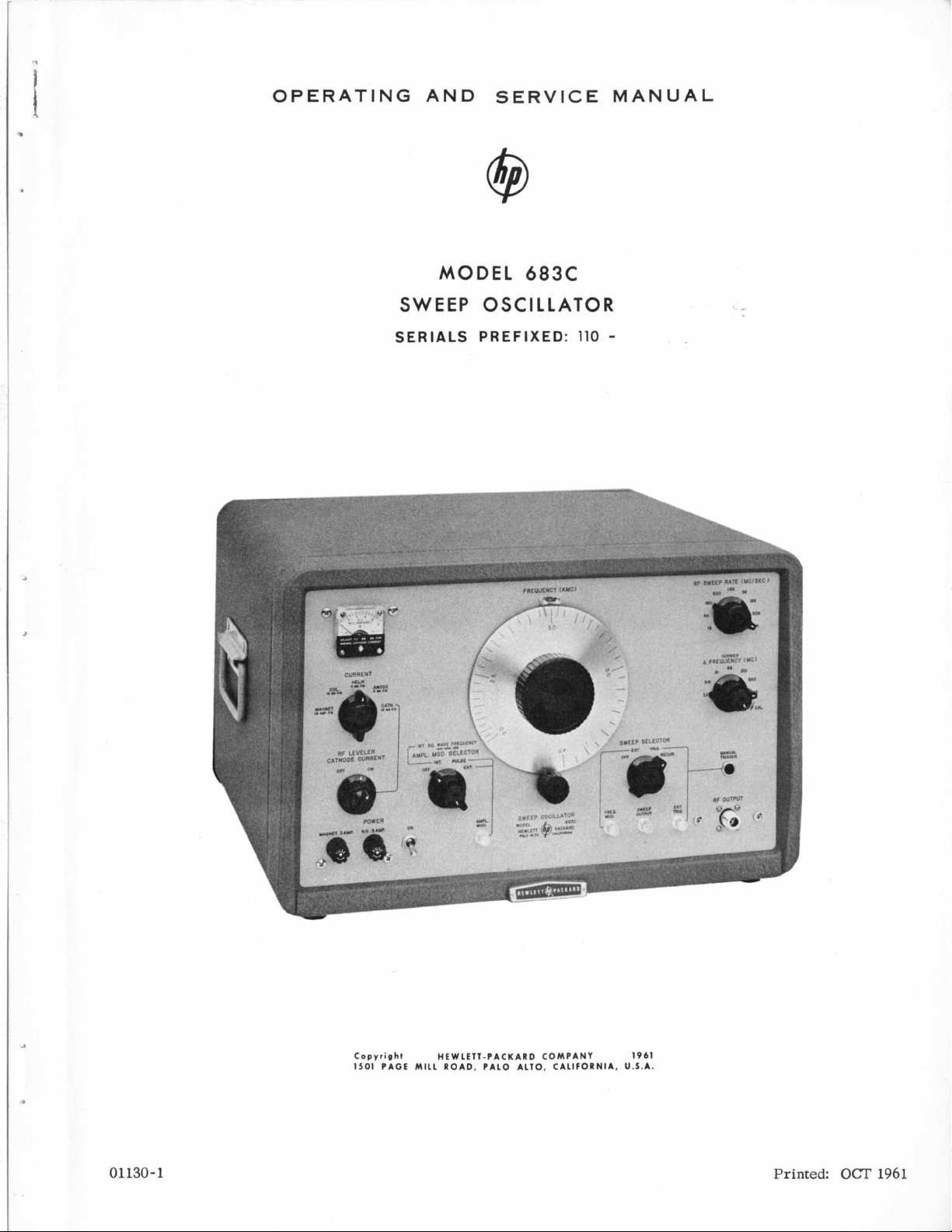
Page 1
3
P
!
OPERATING
AND
SERVICE
MANUAL
MODEL
6a3c
SWEEP OSCILLATOR
SERIALS PREFIXED:
J
110
-
01130-1
Copyright HEWLETT-PACKARD COMPANY
1501
PAGE
MILL
ROAD, PAL0
ALTO,
CALIFORNIA, U.S.A.
1961
Printed:
Om
1961
Page 2
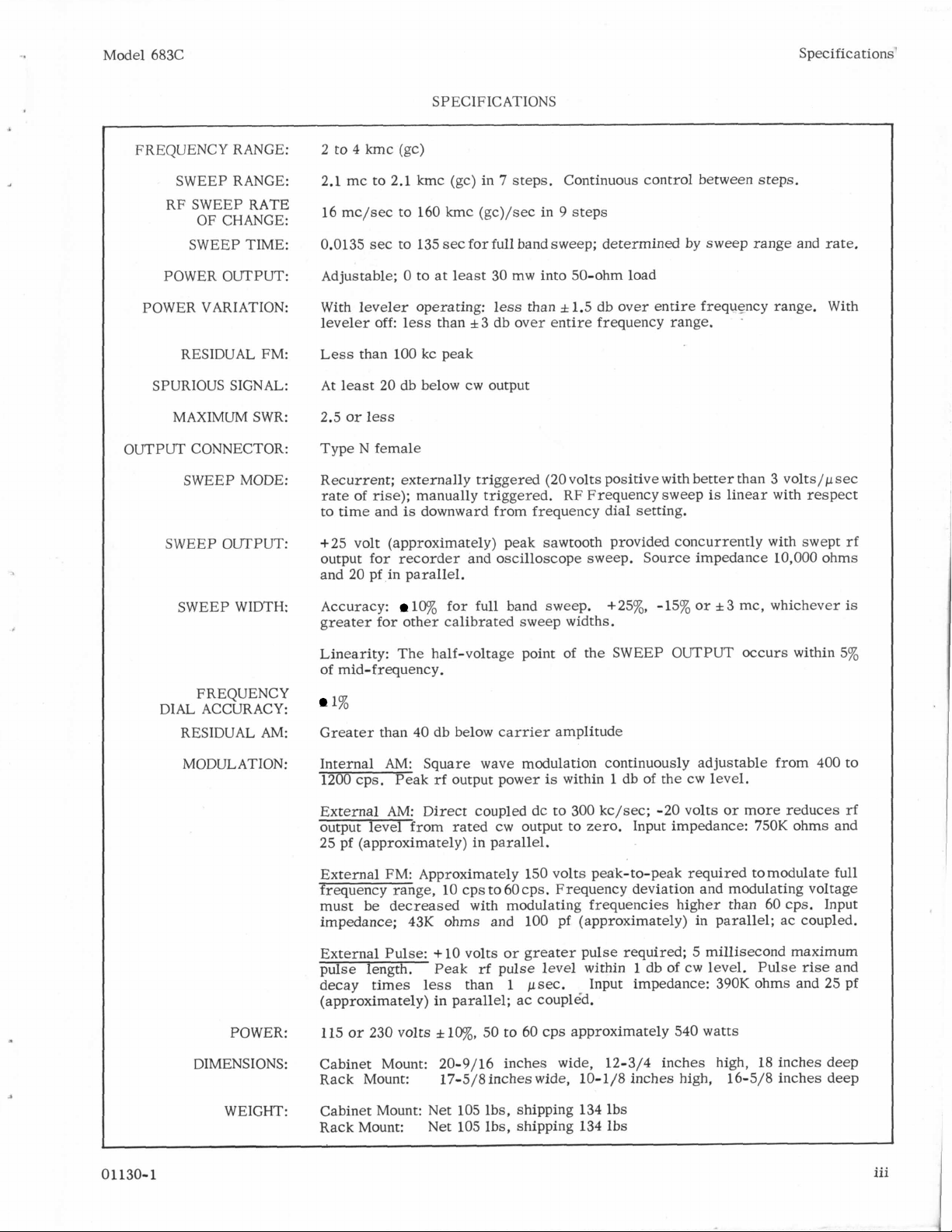
Model 683C Specifications’
SPECIFICATIONS
FREQUENCY RANGE:
SWEEP RANGE:
RF SWEEP RATE
OF CHANGE:
SWEEP TIME:
POWER OUTPUT:
POWER
SPURIOUS SIGNAL:
OUTPUT CONNECTOR:
VARIATION:
RESIDUAL FM:
MAXIMUM SWR:
SWEEP MODE:
SWEEP OUTPUT:
2 to 4 kmc (gc)
2.1 mc to 2.1 kmc (gc) in
16 mc/sec to 160 kmc (gc)/sec in 9 steps
0.0135
Adjustable;
With leveler operating:
leveler
Less than 100
At least 20 db below
2.5 or
Type N female
Recurrent; externally triggered (20 volts positive with better than 3 volts/psec
rate
to time and
+25 volt (approximately) peak sawtooth provided concurrently with swept
output for recorder and oscilloscope sweep. Source impedance 10,000 ohms
and 20 pf in parallel.
sec
to 135
sec
0
to
at least 30 mw into 50-ohm load
off:
less
than & 3 db over entire frequency range.
kc
peak
less
of
rise); manually triggered. RF Frequency sweep
is
downward from frequency dial setting.
7
steps. Continuous control between steps.
for full band sweep; determined by sweep range and rate.
less
cw
than f 1.5 db over
output
entire
frequency range.
is
.
linear with respect
With
rf
SWEEP WIDTH:
FREQUENCY
DIAL ACCURACY:
RESIDUAL AM:
MODULATION:
POWER:
Accuracy:
greater for other calibrated sweep widths.
Linearity: The half-voltage point of the SWEEP OUTPUT occurs within
of mid-frequency.
1%
Greater than 40 db below carrier amplitude
Internal
1200 cps. Peak
External AM: Direct coupled dc to 300 kc/sec; -20 volts or more reduces
output
25 pf (approximately) in parallel.
External FM: Approximately 150 volts peak-to-peak required to modulate full
frequency range, 10 cps to 60 cps, Frequency deviation and modulating voltage
be decreased with modulating frequencies higher than 60 cps. Input
must
impedance; 43K ohms and 100 pf (approximately) in parallel; ac coupled.
External Pulse:
pulse length.
decay times
(approximately) in parallel; ac coupl6d.
115 or 230 volts
AM:
level
10%
for full band sweep.
Square wave modulation continuously adjustable from 400 to
rf
output power
from rated
+
10 volts or greater pulse required: 5 millisecond maximum
Peak
less
f
lvo,
cw
rf
than 1 psec. Input impedance: 390K ohms and 25 pf
50
is
output to zero. Input impedance: 750K ohms and
pulse level within 1 db of
to 60 cps approximately 540 watts
+25%, -15% or
within 1 db of the
&
3
mc, whichever
cw
level.
cw
level. Pulse
rise
is
5%
rf
and
0
1130-
1
DIMENSIONS:
WEIGHT:
Cabinet Mount: 20-9/16 inches wide, 12-3/4 inches high, 18 inches deep
Rack Mount: 17-5/8inches wide,
Cabinet Mount: Net 105 lbs, shipping 134 lbs
Rack Mount:
Net
105 lbs, shipping 134 lbs
10-1/8
inches high, 16-5/8 inches deep
iii
Page 3
Table of Contents
List of Tables
Model 683C
TABLE
Section Page
I
GENERAL INFORMATION
1.1
.
Description
1.2
.
Instrument Cooling System.
1.3
.
Three-Conductor Power Cable
1.4
.
1.5
1.6
I1
OPERATING INSTRUCTIONS
2.1
2.2
2.3
2.4
2.5
2.6
2.7
2.8
111
THEORY OF OPERATION
3-
3.2
3.3
3.4
3.5
3.6
3.7 . Helix Supply Reference Voltage and
3.8
3.9
230-Volt
.
Rack Mounting Instructions
.
BWOTube Information
.
Contents
.
Installation
.
Turn-On Procedure
Using the Sweep Oscillator
.
a CW Signal Source
.
Sweep Operation of the Oscillator
.
Amplitude Modulating the Oscillator
Frequency Modulating the Oscillator
.
.
Application
1
.
Contents
.
Backward-Wave Oscillator Tube
.
RF Leveler and Anode
Reference Circuit
.
Amplitude Modulator
.
Helix Modulator
.
Linear Sweep Generator
Exponential Voltage Generators
.
Regulated Power Supplies
.
Magnet Current Supply (Regulated)
...........
...
. .
Operation
.......
...
.....
............
...........
.......
as
......
.
..........
............
.
.......
......
.........
.....
.
....
1-1
1-1
1-1
1-2
1-2
1-3
2-
1
2-1
2-
1
2-2
2-2
2-2
2-2
2-8
3-
1
3-1
3-3
3-4
3-5
3-5
3-8
3-10
3-11
OF
CONTENTS
Section
IV
MAINTENANCE
4.1
.
General
4.2
.
General Precautions
4.3
4.4
4.5
4.6
4.7
4.8
4.10
4.11
4.12
4.13
4.14
4.15
4.16
4.17
4.18
4.19
4.20
4.21
V REPLACEABLE PARTS
5.1
5.2
Air Filter
.
.
Cabinet Removal
Quick-Check Procedure
.
.
Maintenance
Required
.
Magnet Supply (Regulated)
-150
.
.
Helix Supply
Filament Regulated
.
Measurement of Linear SweepTimes 4-9
.
Replacement
.
Calibration Procedure
RF Sweep Linearity
.
.
Square-Wave Generator
RF
.
Voltage Adjustment
.
Servicing the Sweep Circuits
Replacing Neon DC Coupling
.
Elements
Positioning Frequency Dial on
.
Potentiometer Shaft
.
Tube Replacement
.
Troubleshooting Procedure
.
Introduction
.
Ordering Information
...........
.....
..........
.......
....
Test
Equipment
.........
...
Volt Regulated Supply
.
..........
......
of
BWO Tube. and
...
.....
....
Leveler and Reference Anode
.....
. .
.........
.....
......
.
.........
.....
.
.
Page
c
4-1
4-1
4-2
4-2
4-2
4-6
4-6
4-7
4-7
4-9
4-10
4-14
4-15
4-15
4-17
4-19
4-19
4-22
4-22
5-1
5-1
iv
Number
1.1
.
Electronic Sweep Oscillators
3.1
.
Condition of
RF Sweep
4
.
1
.
Tube Replacement
4.2
.
Troubleshooting Procedure
5.1
.
Replaceable
Tubes
..
Parts
LIST
OF
TABLES
Title
........
During CW and
............
Chart
..........
.........
.............
Page
1-1
3-9
4 . 23
4-24
5-1
01130-1
Page 4
Model 683C
LIST
OF
ILLUSTRATIONS
List of Illustrations
Number Title Page
1.1
.
2.1
2.2
2.3
2.4
2.5
2.6
2.7
2.8
2.9
2.10
3.1
3.2
3.3
3.4
3.5
3.6
3.7
3.8
3.9
Warranty Sheet
Turn-On Procedure and CW Operation
.
Using the Sweep Oscillator
.
as
a
Internal Sweep Modulation
.
Internal Square-Wave Modulation
.
External Pulse Modulation
.
External Amplitude Modulation
.
External Frequency Modulation
.
Allowable External Frequency
.
Suitable Setup for Measuring
.
Input and Output Connector
.
Backward- Wave Oscillator
.
Block Diagram Model 683C
.
RF
.
Adjustable Segments of
.
RF Leveler Circuit
.
Amplitude Modulation EXT
.
Frequency Modulator Waveforms
.
Simplified Schematic
.
Simplified Schematic of
.
CW Signal Source
Modulation Voltage Amplitude vs
Modulation Voltage Frequency
Frequency Deviation Limits when
using External FM
Characteristics
Tube Construction
Sweep Oscillator
Leveler Detected Waveform
(Leveled and Unleveled Positions)
Compensated Helix Voltage
Exponential Sweepcircuit
...........
.
.
.
.
.
2-2
2-3
2-4
2-5
2-6
2-7
2-8
2-9
2-10
3-1
3-2
3-3
3-3
3-4
3-5
3-6
3-7
3-8
......
......
...
......
....
....
...
........
..........
........
..........
....
.........
.
Position
...
of
Sweep Circuit
.....
1-2
2-0
Number
.
4.1
4.2
.
4.3
.
4.4
.
4.5
.
4.6
.
4.7
.
4.8
.
4.9
.
4.10
.
4.11
.
4.12
.
4.13
.
4.14
.
4.15
.
4.16
.
4.17
.
4.18
.
4.19
.
4.20
.
4.21
.
4.22
.
4.23
.
4.24
.
4.25
.
4.26
.
Title
Measuring RF Power Output
Checking Frequency Calibration and
General Performance
Setup for Measuring Residual AM
Measuring Magnet Circuit Ripple
Model 683C Top View
Sweep Output Voltage
Model 683C Bottom View
Model 683C Rear View
Positioning the BWO Tube at the
Front and Rear of Magnet
Calibration Pips on CRO Sweep
Example of Calibration Pips on
CRO Sweep
Crystal Detector-Attenuator
Response Curve
RF
Leveler Circuit Board
RF Leveler Calibration Setup
Model 683C Right Side View
Model 683C
Sweep Output Voltage Linearity
Troubleshooting Chart
Magnet Power Supply
(Current Regulated)
Regulated Primary Power and
Magnet Current Supply
Regulated +300 and -150 Volt PS
Frequency Supply and Low Voltage PS
RF Power Leveler and
Amplitude Modulator
Amplitude Modulator and Anode Section
Exponential and Linear Sweep Gen
Frequency (Helix) Modulator
............
Left
........
........
.........
.........
Side View
........
........
........
.....
.......
...
...
.......
......
....
......
.....
.....
......
....
.......
...
. .
.....
.
Page
4-2
4-3
4-5
4-7
4-8
4-9
4-12
4-12
4-13
4-14
4-15
4-16
4-18
4-19
4-20
4-21
4-22
4-28
4-30
4-31
4-32
4-33
4-34
4-35
4-36
4-37
01130-1
V
Page 5
MODEL 683C
ELECTRONIC SWEEP OSCILLATOR
Model 683C
*
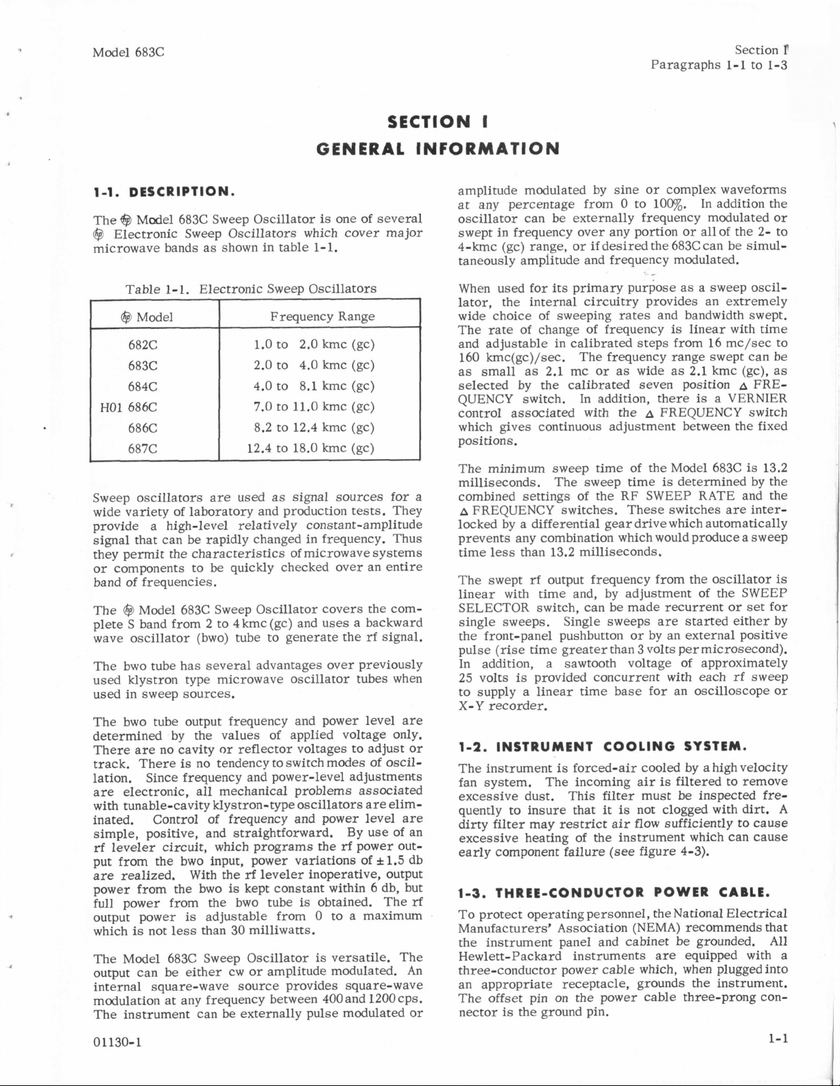
This manual specifically describes Model 683C of the
683C sweep oscillators. If, however, the serial number of your instrument
TllO
series, and
in
general describes all
is
prefixed by TO24
or T044, there are parts of themanual which do not apply to your instrument. If your instrument
carries one of these serial numbers, information specific to your instrument
is
furnished with
this manual. This supplementary material includes schematics, parts list, and replacement
paragraphs and illustrations for those items in the manual that do not describe your instrument.
The supplementary data
is
indexed; paragraph and figure numbers are the same as those used
in the manual for the corresponding information.
If
it
is
necessary to order replacement parts, consult the supplementary
the component
always
use
the part number in your supplementary parts list.
is
not listed,
use
the part number given in section V of the manual; otherwise,
parts
list first.
If
vi
01
130-
1
Page 6
Model 683C
Paragraphs
Section
1-1
to
T
1-3
SECTION
GENERAL INFORMATION
1-1.
DESCRIPTION.
The @ Model 683C Sweep Oscillator
($3
Electronic Sweep Oscillators which
microwave bands as shown in table
Table 1-1. Electronic Sweep Oscillators
($9
Model
682C
683C
684C
H01
686C
686C
687C
Sweep oscillators are used as signal
wide variety of laboratory and production tests. They
provide a high-level relatively constant-amplitude
signal that can be rapidly changed in frequency. Thus
they permit the characteristics of microwave systems
or components to be quickly checked over an entire
band of frequencies.
The
@
Model 683C Sweep Oscillator covers the com-
plete
S
wave oscillator (bwo) tube to generate the
The bwo tube has several advantages over previously
used klystron type microwave oscillator tubes when
used in sweep sources.
The bwo tube output frequency and power level are
determined by the values of applied voltage only.
There are no cavity or reflector voltages to adjust or
track. There
lation. Since frequency and power-level adjustments
are electronic, all mechanical problems associated
with tunable-cavity Hystron-type oscillators are
inated. Control of frequency and power level are
simple, positive, and straightforward. By
rf
put from the bwo input, power variations of i1.5 db
are realized,
power from the bwo
full power from the bwo tube
output power
which
The Model 683C Sweep Oscillator
output can be either
internal square-wave source provides square-wave
modulation at any frequency between 400and 12OOcps.
The instrument can be externally pulse modulated or
band from 2 to 4 kmc (gc) and
is
no tendency to switch modes of oscil-
leveler circuit, which programs the
With
the
is
is
adjustable from 0 to a maximum
is
not
less
than 30 milliwatts.
cw
Frequency Range
1.0 to 2.0 kmc (gc)
2.0 to 4.0 kmc (gc)
4.0 to 8.1 kmc (gc)
7.0 to 11.0 kmc (gc)
8.2 to 12.4 kmc (gc)
12.4 to 18.0 kmc (gc)
rf
leveler inoperative, output
kept constant within 6 db, but
or amplitude modulated. An
is
one of several
cover
1-1.
sources
uses
a backward
rf
rf
power out-
is
obtained. The
is
versatile. The
signal.
use
major
for a
elim-
of
an
rf
I
amplitude modulated by
at any percentage from
oscillator can be externally frequency modulated or
swept
in
frequency over any portion or all
4-kmc (gc) range, or
taneously amplitude and frequency modulated.
When used for
lator, the internal circuitry provides an extremely
wide choice of sweeping rates and bandwidth swept.
The rate
and adjustable in calibrated steps from 16 mc/sec to
160 kmc(gc)/sec. The frequency range swept can be
small as 2.1 mc or as wide as 2.1 kmc (gc), as
as
selected by the calibrated seven position
QUENCY switch. In addition, there
control associated with the
which gives continuous adjustment between the fixed
positions
The minimum sweep time of the Model 683C
milliseconds. The sweep time
combined settings of the RF SWEEP RATE and the
A
FREQUENCY switches. These switches are inter-
locked by a differential gear drive which automatically
prevents any combination which would produce a sweep
time
less
The swept
linear with time and, by adjustment of
SELECTOR switch, can be made recurrent or
single sweeps. Single sweeps are started either by
the front-panel pushbutton or by an external positive
pulse (rise time greater than
In addition, a sawtooth voltage of approximately
25 volts
to supply a linear time base for an oscilloscope or
X-Y
recorder.
1-2.
INSTRUMENT COOLING SYSTEM.
The instrument
fan system. The incoming air
excessive dust. This filter must be inspected
quently to insure that it
dirty
filter
excessive heating of the instrument which can cause
early component failure (see figure 4-3).
1-3.
THREE-CONDUCTOR POWER CABLE.
To protect operating personnel, the National Electrical
Manufacturers’ Association (NEMA) recommends that
the instrument panel and cabinet be grounded. All
Hewlett-Packard instruments are equipped with a
three-conductor power cable which,
an appropriate receptacle, grounds the instrument.
The
offset pin
nector
is
its
primary purpose as a sweep oscil-
of
change of frequency
.
than 13.2 milliseconds.
rf
output frequency from the oscillator
is
provided concurrent with each
is
forced-air cooled by a high velocity
may restrict air flow sufficiently to cause
on
the power cable three-prongcon-
the ground pin.
sine
or complex waveforms
0
to
lOC%.
if
desired the 683C can be simul-
A
FREQUENCY switch
3
volts per microsecond).
is
is
not clogged with dirt.
In addition the
of
the 2- to
is
linear with time
A
is
a VERNIER
is
is
determined by the
the
SWEEP
set
rf
sweep
filtered to remove
when
plugged into
FRE-
13.2
is
for
fre-
A
0
1
130-
1
1-1
Page 7
Section
Paragraphs
I
1-4
to 1-5
To preserve the protection feature when operating
the instrument from a two-contact outlet,
use
a threeprong to two-prong adapter and connect the green
pigtail on the adapter to ground.
1-4.
230-VOLT
The @ Model 683C
operation, but
OPERATION.
is
usually shipped wired for 115 vac
is
quickly and easily converted to
operation from a nominal 230-volt 50/60 cps source.
To convert, remove two jumpers between terminals
A2 and A3.
In
addition, remove the jumper
wire
(connecting the two rear terminals of the MAGNET
AMP and
3
minal of the
minal of
a pink lead attached to
either the MAGNET
the
H.
V.
3
AMP.
fuses)
from the rear
H.V.
fuse and reconnect to the side
H.V.
fuse.
This side terminal also has
it.
Do
not change the size of
fuse
or the
H.V.fuse.
ter-
ter-
When
operating from a 230-volt source, T101, the magnet
supply and the fan operate on 115 volts supplied by
T1
primary windings which act as a 2:l autotransformer. This additional load
load carried by the
sets
the expected reduction in current due to 230-volt
H.V.
is
added to the normal
fuse
and approximately off-
operation.
Model 683C
1-5.
RACK MOUNTING INSTRUCTIONS.
When mounting a rack model instrument, leave at
least three inches clearance behind the air intake to
insure
that the air intake
ment which
proper
is
air
circulation. In addition, be certain
is
not near another piece of equip-
discharging hot air
in
the
vicinity of
the Model 6836 air intake.
The following instructions should be followed for easy
installation of a rack model instrument (683CR)
in
an
equipment rack.
Remove the four
1)
screws
from
the
rear of the
in-
strument cabinet and slide the instrument forward
from the cabinet.
the
2) Mount
empty cabinet
four oval head machine
side
of
1-3/4
the cabinet
inches from the top and bottom edges of the
in
the
in
the equipment rack with
screws:
two
screws
on each
mounting holes approximately
mounting flanges.
3) Raise the instrument chassis and slide it gently
into the cabinet. Be certain the power cable passes
freely through the hole in the rear of the cabinet.
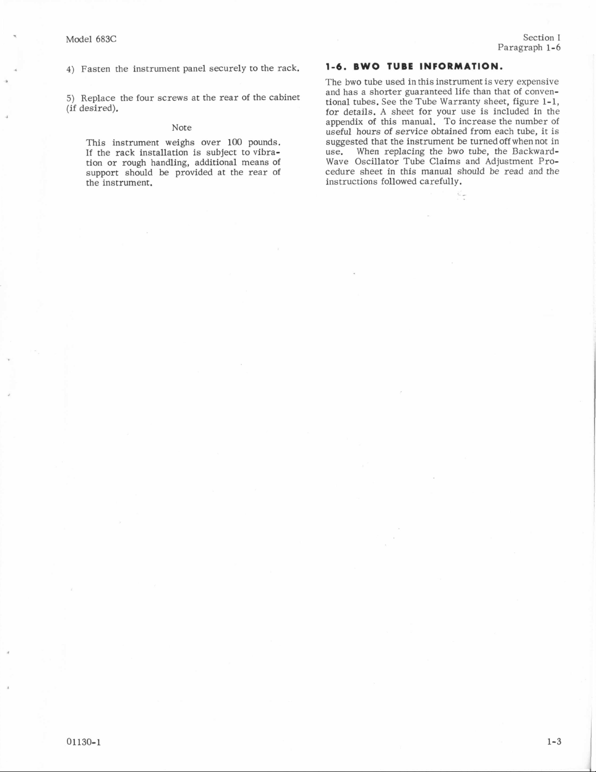
WARRANTY
CLAIM
AND
ADJUSIMINT PROCIDURI
MICROWAVE
INFORMATION
TUBE
WARRANTY CLAIM
Slp.t"re
Title
FORM
9/12/61
Figure
1-1.
Warranty Sheet
1-2 01130-1
Page 8
Model 683C
4)
Fasten the instrument panel securely to the rack.
5)
Replace the four
(if
desired).
This instrument weighs over
If the rack installation
tion or rough handling, additional means of
support should be provided at the rear of
the instrument.
screws
Note
at the rear of the cabinet
100
pounds.
is
subject
to
vibra-
Section
Paragraph 1-6
1-6.
BWO
The bwo tube used in this instrument
and has a shorter guaranteed
tional tubes. See the Tube Warranty sheet, figure
for
details. A sheet for your
appendix of this manual. To
useful
suggested that the instrument be turned off when not in
use.
Wave Oscillator Tube Claims and Adjustment Pro-
cedure sheet in this manual should be read and the
instructions followed carefully.
hours of
When replacing the bwo tube, the Backward-
TUBE
service
INFORMATION.
is
very expensive
life
than that of conven-
use
is
increase
obtained from each tube, it
included in the
the number
1-1,
of
is
I
01130-1
Page 9
Section I1
Figure 2-1
Model 6836
9.
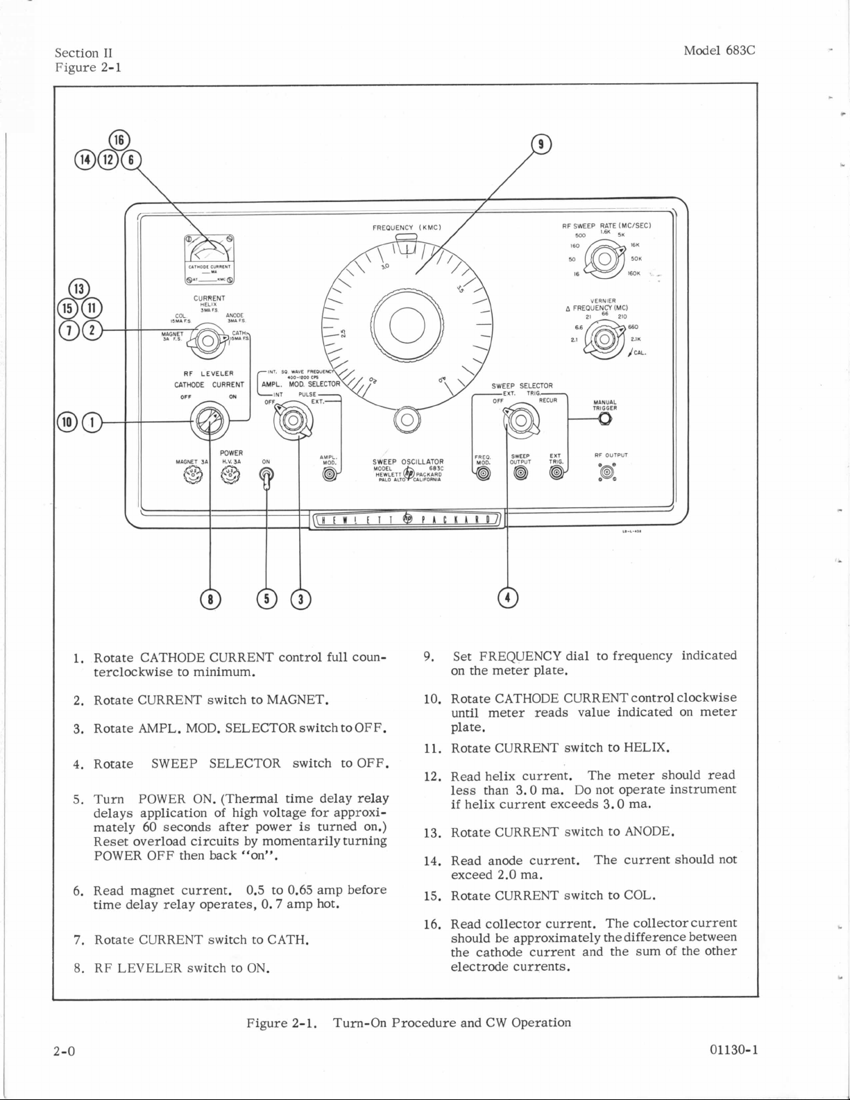
1.
Rotate CATHODE CURRENT control
terclockwise to minimum.
2. Rotate CURRENT switch to MAGNET.
3. Rotate AMPL. MOD. SELECTOR switch toOFF.
4. Rotate SWEEP SELECTOR switch to
5. Turn POWER ON. (Thermal time delay relay
delays application of high voltage for approxi-
mately 60 seconds after power
Reset overload circuits by momentarily turning
POWER
6.
Read magnet current.
time delay relay operates,
7.
Rotate CURRENT switch to CATH.
8.
RF LEVELER switch to
2-0 01130-1
OFF
then back “on”.
0.5
to 0.65 amp before
0.7
amp hot.
ON.
Figure 2-1.
full
coun-
OFF.
is
turned on.)
Turn-On Procedure and CW Operation
Set FREQUENCY dial to frequency indicated
on the meter plate.
10. Rotate CATHODE CURRENT control clockwise
until meter reads value indicated on meter
plate.
11.
Rotate CURRENT switch to HELIX.
12. Read helix current. The meter should read
less
than
3.0
ma. Do not operate instrument
if
helix current exceeds
13.
Rotate CURRENT switch to ANODE.
14. Read anode current. The current should not
exceed 2.0 ma.
15.
Rotate CURRENT switch to COL.
16. Read collector current. The collector current
should be approximately the difference between
the cathode current and the sum of the other
electrode currents.
3.0
ma.
Page 10
Model 683C
Paragraphs 2-1 to 2-3
Section I1
SECTION
OPERATING INSTRUCTIONS
2-1.
CONTENTS.
Section
operating the sweep oscillator, instructions for modulating the
cations of the instrument.
2-2.
The Model 683C Sweep Oscillator should be placed on
a work bench or table with at least 3 inches of clearance at
the filter. To avoid seriously restricted air flow,
be careful not to let loose pieces of paper, etc.
main in the rear area since they can be pulled against
the air filter.
The power cable should be used in a NEMA approved
standard three-prong grounding receptacle (paragraph 1-3).
Complete installation instruction for rack model
struments are given in paragraph 1-5.
2-3.
Good operating practice dictates that you follow ,a
given step-by-step procedure when turning on the
Model 683C, to protect the bwo tube. This routine
will
critical circuits to insure normal operation.
Under normal operation no damage can be done by
improper setting of front panel controls since builtin
high-voltage transformer
in
by momentarily turning off power to the instrument.
In addition to the overload protection, internal
driver-adjust controls preset limits on front panel
controls to safe values. BWO tube currents aremonitored with built-in metering circuits, which provide
a positive check that the bwo tube
in
To place the instrument in operation, the steps outlined
in
Additional data on some of the steps are given below
under STEPS; before performing the turn-on procedure
for the first time, read this supplemental information.
Figure 2-1 shows the front panel controls as
briefly describing the steps of the turn-on procedure.
The unnumbered controls and terminals can be oper-
ated in any order desired, depending on the type of
operation selected. Characteristics of the input and
output connectors are given
With the completion of the turn-on procedure the instrument
set
I1
contains instructions for setting up and
rf
output, and a discussion of some appli-
INSTALLATION.
the
rear to insure adequate air flow through
re-
in-
TURN-ON PROCEDURE.
systematically check out proper operation of all
overload protection cuts off primary power to the
if
excessive current flows
the helix circuit. The overload circuits are reset
screw-
is
being operated
a safe manner.
figure 2-1 should be followed in the order given.
well
as
in
figure 2-10.
is
set
up for
on the FREQUENCY dial. Once
cw
operation at the frequency
cw
operation has
II
been established, the oscillator may be adjusted for
frequency and for amplitude modulation (paragraphs
2-4 through 2-7).
Until thoroughly familiar with instrument operation,
it
is
recommended that you
information which follows.
STEPS:
The number associated with each paragraph
the turn-on procedure step under discussion. See
figure 2-1 for
5. Set POWER to ON. The plastic graticule at the
top of the FREQUENCY dial
fan
will
delays application of high voltage to the main
cuits approximately 60 seconds after
ment
are partly energized when the POWER switch
turned on, but do not regulate until the time-delay
switch has operated and the filaments
lator circuits are energized.
6. Read magnet current on the monitor meter. The
current should be 0.5 to 0.65 ampere when
turned on and
after a
ATE INSTRUMENT IF AFTER WARMUP THE
MAGNET CURRENT
AND
8.
With RF LEVELER switch to
have a power output variation across the band of
i1.5 db or
tion the power variation across the band will not
exceed
9.
It
is
cathode current at the frequency indicated on the
meter plate. The reasons are: a) Only with the
rated cathode current at the frequency specified
will
conditions are not met, the RF LEVELER
give the desired leveling action
10.Rotate CATHODE CURRENT control in a clock-
wise
Normal (at least 30 milliwatts) output
tained with the value of cathode current stamped
on the panel meter. (The maximum
limited by internal adjustments.)
12.Read helix current. The current should be
than 3 ma. DO NOT OPERATE THE INSTRUMENT IF THE HELIX CURRENT EXCEEDS 3MA.
An
overload relay prevents excessive helix
rent. To
POWER off, then back to ON. Excessive helix
current may indicate misalignment of the bwo tube
in
the magnetic field
the
steps not discussed below.
operate.
is
energized. The magnet supply
will
few
minutes operation. DO NOT OPER-
0.725
AMPERE.
less.
3
db.
important that the meter reads the exact
adequate power be produced. b) If the latter
direction and observe the current reading.
reset
refer
to the supplemental
refers
will
glow. The cooling
A
thermal time-delay switch
cir-
the
instru-
circuits
in
the regu-
first
gradually settle to 0.70 ampere
IS
NOT BETWEEN 0.675
ON
the 683C
In the RF LEVELER OFF posi-
(+
1.5 db).
will
current
will
be ob-
less
will
not
is
cur-
the relay, momentarily turn
(see
section IV, Maintenance).
to
is
01130-1
2-
1
Page 11
I
Section
I1
Paragraphs 2-4 to 2-7
Verify proper operation of the helix power supply
by rotating the FREQUENCY dial from 2 to 4 kmc
(gc) and noting that there
current. (BWO
in
helix voltage.
helix
Thus
as the FREQUENCY dial
range
is
a check that helix voltage
16. The collector
ference
current
between cathode current and
the helix and anode current readings.
is
a variation
in
helix
current varies with a change
a variation
in
helix
is
turned through
is
current
its
changing.)
reading should be the dif-
the
sum of
If
there
is
a large difference between this value of collector
current and that shown by the meter,
ment
is
not functioning properly
The instrument
ting a 30 milliwatt or more
is
now operating normally and genera-
cw
signal at the frequency
(see
the
instru-
section
IV).
indicated by the FREQUENCY dial.
2-4.
ment is
the AMPL. MOD. SELECTOR switch
LEVELER to ON.
is
of better than
The output power level
USING THE SWEEP OSCILLATOR AS
A CW SIGNAL SOURCE.
Upon completion of the turn-on procedure, the
set
up for cw operation. However, check that
is
OFF; RF
In
cw operation, output frequency
indicated by the FREQUENCY dial to an accuracy
-+
1%.
is
adjustable from at least
instru-
30 milliwatts down to zero by theCATHODE CURRENT
control. Monitor
the power level near rated value to
ratings are not being exceeded.
higher than 7 ma
helix
current
to 7 ma and check that helix current
This
is
a
check
the bwo
is
discussed in paragraph 4-13B.)
the
cathode current when adjusting
insure
If
cathode current
is
required to get rated power, and
is
higher than 3 ma, set cathode
is
less
that tube
focus
is
correct.
that tube
current
than 3 ma.
(Focusing
By the addition of a precision attenuator, the 683C can
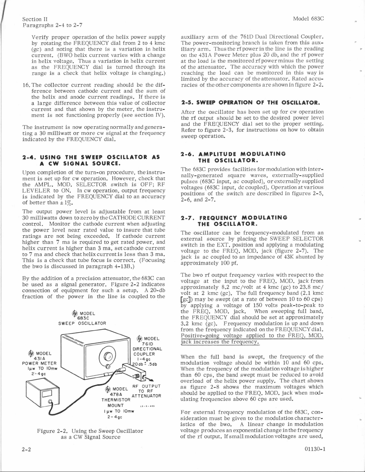
be used as a signal generator. Figure 2-2 indicates
connection of equipment for such a setup.
fraction of the power
SWEEP OSCILLATOR
POWER METER
lpw TO lOmw
2-4gc
in
@gyL
the line
THERMISTOR
MOUNT
Ipw
TO
2-
4gc
is
IOmw
A
20-db
coupled to the
DIRECTIONAL
COUPLER
I
-4gc
cdb .5db
Figure 2-2. Using the Sweep Oscillator
as a CW Signal Source
Model 683C
auxiliary arm of
The power-monitoring branch
iliary arm. Thus the
on the 431A Power Meter plus 20 db, and the
at the load
is
the
761D Dual Directional Coupler.
is
taken from this aux-
rf
power in the
line
is
the reading
rf
power
the monitored rfpower minus the setting
of the attenuator. The accuracy with which the power
reaching the load can be monitored in this way
is
limited by the accuracy of theattenuator. Rated accuracies of the other components are shown
2-5.
SWEEP OPERATION
OF
THE OSCILLATOR.
After the oscillator has been set up for
the
rf
output should
be
set
to the desired power level
in
figure 2-2.
cw
operation
and the FREQUENCY dial set to the proper setting.
Refer
to figure 2-3, for instructions on how to obtain
sweep operation.
2-6.
AMPLITUDE MODULATING
THE OSCILLATOR.
The 683C provides facilities for modulation with internally-generated square waves, externally-supplied
pulses (683C input, ac coupled), or externally supplied
voltages (683C input, dc coupled). Operation at various
positions of the switch are described
in
figures 2-5,
2-6, and 2-7.
2-7.
FREQUENCY MODULATING
THE OSCILLATOR.
The oscillator can be frequency-modulated from an
external source by placing the SWEEP SELECTOR
switch
in
the
EXT. position and applying a modulating
voltage to the FREQ. MOD. jack (figure 2-7). The
jack
is
ac coupled to an impedance of 43K shunted by
approximately 100 pf.
The bwo
rf
output frequency varies with respect to the
voltage at the input to the FREQ. MOD. jack from
approximately 8.2 mc/volt at 4 kmc (gc) to 23.8 mc/
volt at 2 kmc (gc). The full frequency band (2.1 kmc
[gcJ) may be swept (at a rate of between
10
to 60 cps)
by applying a voltage of 150 volts peak-to-peak to
the FREQ.
MOD.
jack. When sweeping full band,
the FREQUENCY dial should be set at approximately
3.2 kmc (gc). Frequency modulation
is
up and down
from the frequency indicated on the FREQUENCY dial.
Positive-going voltage applied to the FREQ. MOD.
iack increases the freauencv.
is
When the full band
swept, the frequency of the
modulation voltage should be within 10 and 60 cps.
When
the frequency of the modulation voltage
is
higher
than 60 cps, the band swept must be reduced to avoid
overload of the helix power supply.
The
chart shown
as figure 2-8 shows the maximum voltages which
should be applied to the FREQ. MOD. jack
when
mod-
ulating frequencies above 60 cps are used.
For external frequency modulation of the 683C, consideration must be given to the modulation character-
istics
voltage produces an exponential change
of the
of the bwo.
rf
output.
If
A
linear change
in
modulation
in
the frequency
small modulation voltages are used,
2-2
01130-1
Page 12
Model 683C
COL
CURRENT
HELIX
,wr,
ANODE
RF
SWEEP
RATE
IMC/SECI
Section
Figure 2-3
-0
-0
I1
3A
POWER
H.V.
3A
MAGNET
First turn on instrument and adjust for normal out-
put
under
cw
operation as shown in the turn-on
procedure (figure 2-1).
1.
Rotate the AMPL.
OFF,
or other desired mode.
2. Set FREQUENCY (KMC) dial to
(sweep
is
downward from FREQUENCY dial
MOD.
SELECTOR switch to
4
kmc (gc)
setting).
3.
Rotate A FREQUENCY switch to position cor-
responding to number of megacycles to be
swept. Set VERNIER to CAL. For variable
segments
4.
Rotate the RF SWEEP RATE switch totheposi-
of A FREQUENCY, rotate out of CAL.
tion corresponding to the rate of sweep desired
in mc/sec.
The
A
FREQUENCY switch and the RF SWEEP
RATE switch are mechanically interlocked to
prevent a combination
result in a sweep time of
of
settings that would
less
than 0.0137
second.
5.
Rotate SWEEP SELECTOR switch to RECUR
if
automatically recurring sweeps are desired.
6.
Rotate SWEEP SELECTOR switch to
TRIG.
single sweeps are desired. Sweeps may be
started by momentarily pressing MANUAL
TRIGGER button, or by supplying a positive
20-volt pulse to Em. TRIG. jack.
CHARACTERISTICS
-
Direction:
RF sweeps are downward, starting at the
quency indicated on the FREQUENCY (KMC)
dial.
SWEEP OUTPUT voltage
is
a positive going
20-25 volt sawtooth voltage.
Accuracy:
Frequency band swept
sweep. +25%, -15% or
greater, for sweep widths
is
within
i3
mc, whichever
less
f
10%
than full band.
for
if
fre-
full
is
O
1130-
~~
Figure 2-3. Internal Sweep Operation
1
2-3
Page 13
Section
I1
Figure 2-4
Model 683C
RF
LEVELER
CATHODE CURRENT
FREQUENCY
(KMC)
RF SWEEP RATE (MCISECI
SW
5%
VERNIER
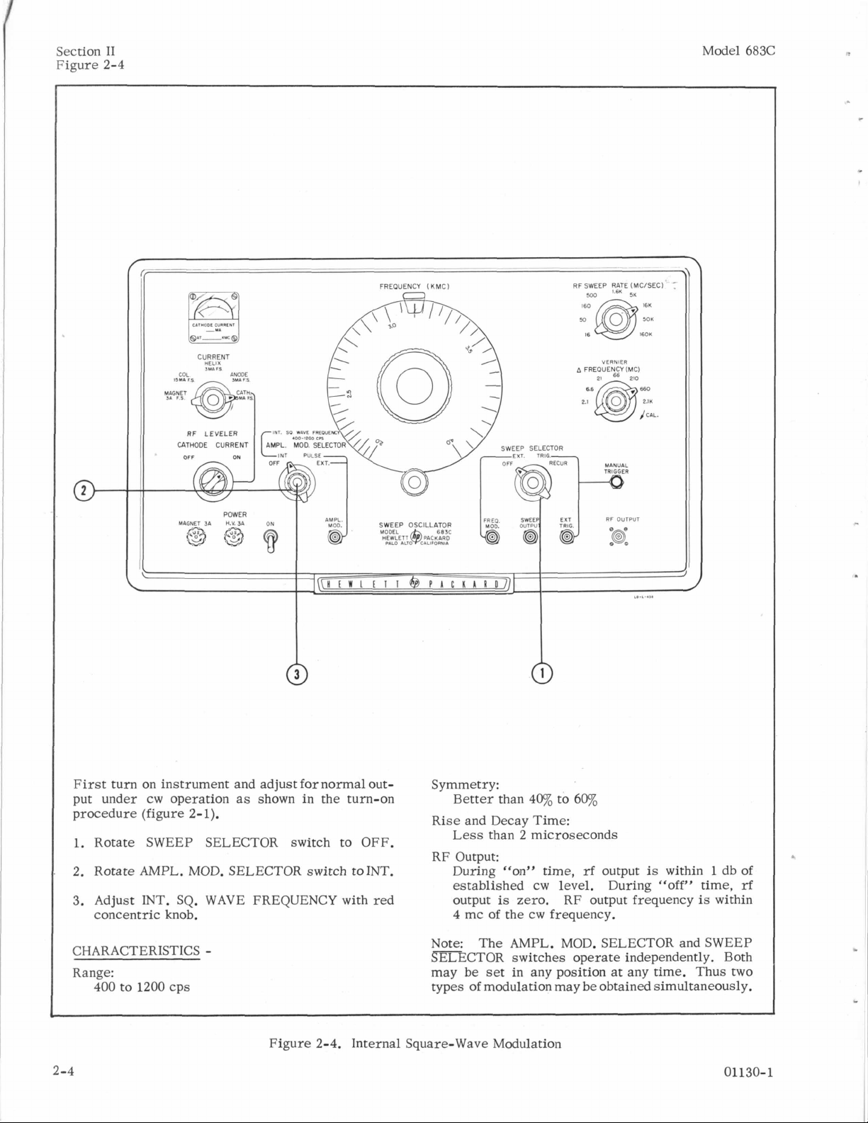
First turn on instrument and adjust
for
normal output under cw operation as shown in the turn-on
procedure (figure 2-1).
1.
Rotate SWEEP SELECTOR switch to OFF.
2. Rotate AMPL. MOD. SELECTOR switch toINT.
3.
Adjust
INT.
SQ. WAVE FREQUENCY with red
concentric knob.
CHARACTERISTICS
-
Range:
400 to 1200 cps
Figure
2-4.
2-4
Symmetry:
Better than 4v0
Rise and Decay
Time:
Less than 2 microseconds
RF Output:
During "onyy time,
established
output
4
mc
of
cw
is
zero. RF output frequency
the
cw
frequency.
Note: The AMPL. MOD. SELECTOR and SWEEP
SELECTOR switches operate independently. Both
may be
types
set
in any position at any time. Thus two
of
modulation may be obtained simultaneously.
Internal Square-Wave Modulation
to
60%
rf
output
level. During
is
within 1 db
"off"
time,
is
within
01
of
rf
130-
1
Page 14
Model 683C
Section
Figure 2-5
I1
First turn on instrument and adjustfor normal output under
procedure (figure 2-1).
1.
Rotate SWEEP SELECTOR switch to OFF.
2. Rotate AMPL. MOD. SELECTOR switch to
PULSE.
3.
a) Feed
or
to
b)
be applied to the AMPL. MOD. jack.
01130-
1
cw
operation as shown in the turn-on
a
+
10
to
+30
volt signal, 5 milliseconds
less
in width, at frequencies from
300
kc into the AMPL. MOD. jack.
A
square wave
-10
volts
100
or
more can also
Figure 2-5. External Pulse Modulation
cps
CHARACTERISTICS
RF
Output:
During "on" time,
established
output
4
Note: The AMPL. MOD. SELECTOR and SWEEP
-
SELECTOR switches operate independently. Both
may be set in any position
types
is
zero. RF output frequency
mc
of
the cw frequency.
of
modulation may be obtained simultaneously.
-
rf
cw
level. During "off" time,
output
is
within 1 db
at
any time. Thus two
is
of
rf
within
2-5
Page 15
Section
I1
Figure 2-6
RF
SWEEP RATE (MCISEC)
yI0
5x
Model 683C
CURRENT
HELIX
,udrs
COL
RF
CATHODE CURRENT
OFF
LEVELER
ANODE
3YA
@
31
POWER
n.v.m
MAGNET
16
FS
I601
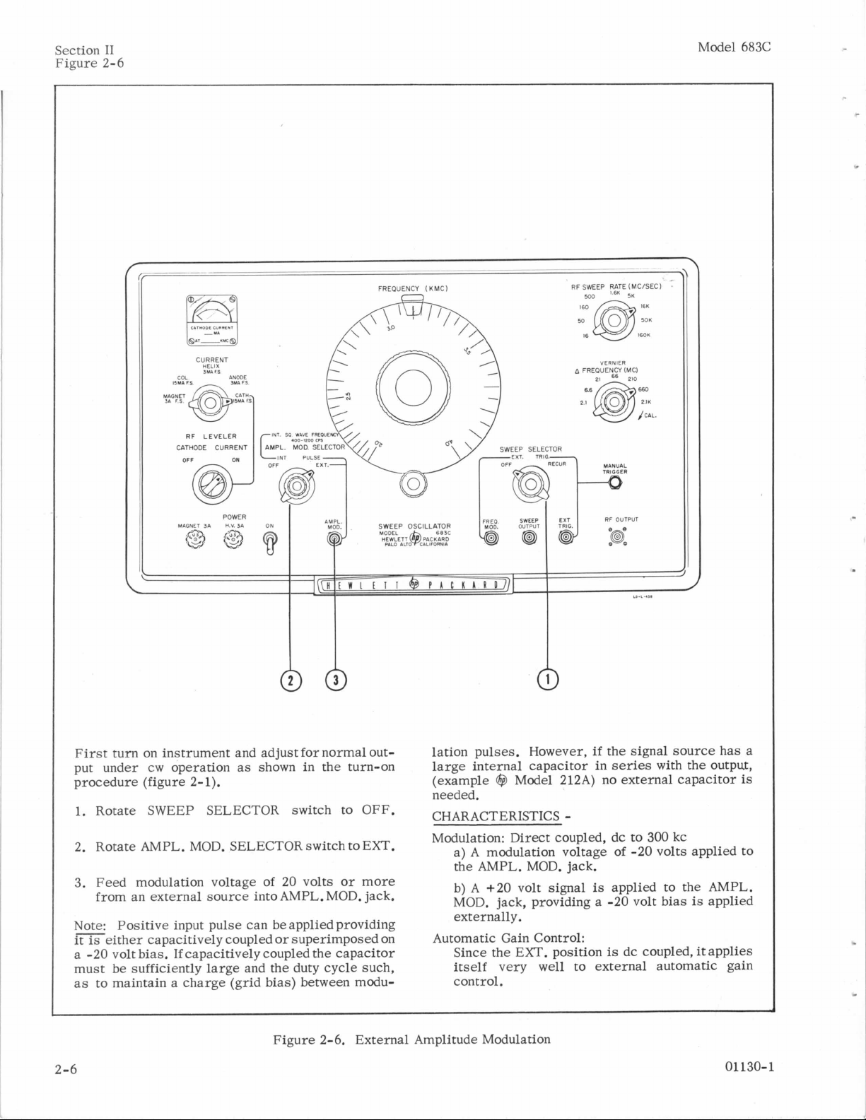
First turn on instrument and adjust for normal output under
procedure (figure 2-
cw
operation as shown
1).
in
the turn-on
lation pulses. However,
large internal capacitor in
(example
($9
Model 212A) no external capacitor
if
the signal source has a
series
with the output,
needed.
1.
Rotate SWEEP SELECTOR switch to OFF.
2. Rotate AMPL. MOD. SELECTOR switch to EXT.
CHARACTERISTICS
-
Modulation: Direct coupled, dc to 300 kc
a)
A
modulation voltage of -20 volts applied to
the AMPL. MOD. jack.
3.
Feed modulation voltage
from an external source into AMPL. MOD. jack.
Note:
-
Positive input pulse can be applied providing
it is either capacitively coupled or superimposed on
a -20 volt bias.
If
capacitively coupled the capacitor
must be sufficiently large and the duty cycle such,
as to maintain a charge (grid bias) between modu-
of
20 volts or more
b)
A
+20 volt signal
is
applied to the AMPL.
MOD. jack, providing a -20 volt bias
externally.
Automatic Gain Control:
Since the EXT. position
itself very
well
is
dc coupled,
to external automatic gain
control.
is
applied
it
applies
Figure 2-6. External Amplitude Modulation
2-6 01
is
130-
1
Page 16
I
Model 683C
RF
LEVELER
CATHODE CURRENT
FREQUENCY (KMCI
RF SWEEP RAT€ IMCISEC)
VERNIER
Section
Figure 2-7
I1
31
POWER
H.V.3A
MAGNET
@@
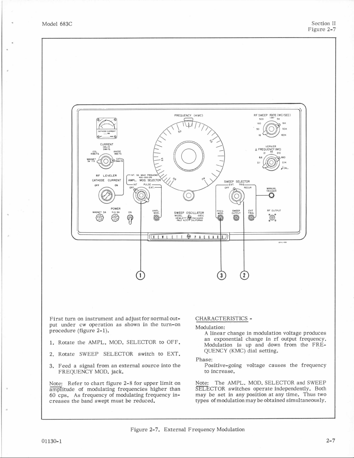
First
turn on instrument and adjust
put under
cw
operation as shown in the turn-on
procedure (figure 2-1).
Rotate the AMPL. MOD. SELECTOR
1.
2. Rotate SWEEP SELECTOR switch to EXT.
3.
Feed a signal from an external source into the
FREQUENCY MOD. jack.
for
normal out-
to
OFF.
CHARACTERISTICS
-
Modulation:
A
linear change in modulation voltage produces
an exponential change in
Modulation
is
up and down from the FRE-
rf
output frequency.
QUENCY (KMC) dial setting.
Phase:
Positive-going voltage causes the frequency
to increase.
Note: Refer to chart figure 2-8 for upper limit on
amplitude of modulating frequencies higher than
60 cps.
As
frequency
of
modulating frequency in-
creases the band swept must be reduced.
Figure
2-7.
01130-1
Note:
The AMPL. MOD. SELECTOR and SWEEP
SELECTOR switches operate independently. Both
may be
set
in any position at any time. Thus two
types of modulation may be obtained simultaneously.
External Frequency Modulation
2-7
Page 17
Section 11
Model 683C
Paragraph 2-8
the
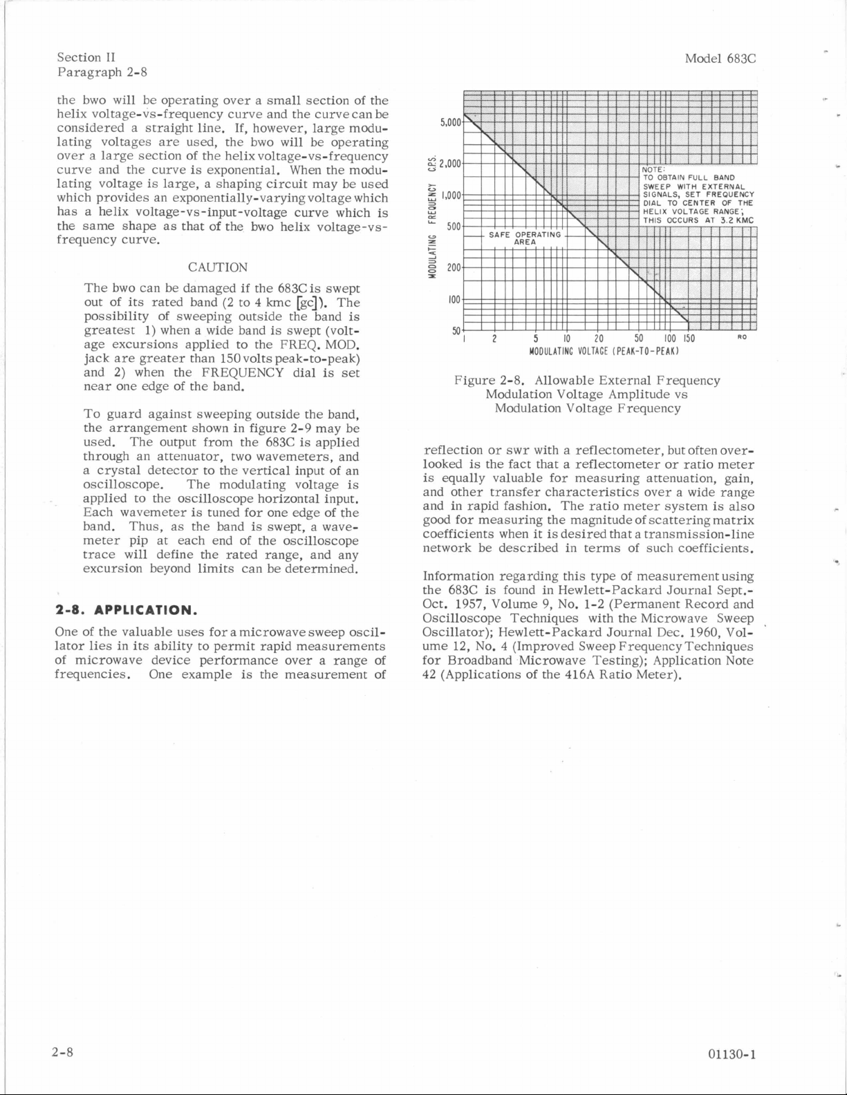
bwo will be operating over a small section of the
helix voltage-vs-frequency
considered a straight
curve
and the
line.
If, however, large modu-
curve
can be
lating voltages are used, the bwo will be operating
over a large section of the helix voltage-vs-frequency
curve and
lating voltage
the
curve
is
large, a shaping
is
exponential. When the modu-
circuit
may be used
which provides an exponentially-varying voltage which
has a helix
the same shape as that
voltage-vs-input-voltage
of
the bwo helix voltage-vs-
curve which
is
frequency curve.
CAUTION
The bwo can be damaged if
out of its rated band (2 to
possibility of sweeping outside
greatest 1) when a wide band
age excursions applied to the FREQ. MOD.
jack are greater than 150 volts peak-to-peak)
and
2)
when the FREQUENCY dial
near one edge of
the
band.
To guard against sweeping outside the band,
the arrangement shown
used. The output from
through an attenuator, two wavemeters, and
a crystal detector to the vertical input of an
oscilloscope. The modulating voltage
applied to the oscilloscope horizontal input.
Each wavemeter
band. Thus, as
is
tuned for one edge of the
the
meter pip at each end of the oscilloscope
trace will define the rated range. and any
excursion beyond limits can be ietermined.
2-8.
APPLICATION.
the
683Cis swept
4
kmc [gc]). The
is
swept (volt-
in
figure 2-9 may be
the
683C
band
is
swept, a wave-
the
is
band
is
set
applied
is
is
5
10
20
50
100
150
MODULATING VOLTAGE (PEAK-TO-PEAK)
RO
Figure 2-8. Allowable External Frequency
Modulation Voltage Amplitude
vs
Modulation Voltage Frequency
reflection or
looked
is
equally valuable for measuring attenuation, gain,
swr
with a reflectometer, but often over-
is
the fact that a reflectometer or ratio meter
and other transfer characteristics over a wide range
and
in
rapid fashion. The ratio meter system
is
also
good for measuring the magnitude of scattering matrix
coefficients when it
is
desired that a transmission-line
network be described in terms of such coefficients.
Information regarding this type of measurement using
the 683C
is
found in Hewlett-Packard Journal Sept.Oct. 1957, Volume 9, No. 1-2 (Permanent Record and
Oscilloscope Techniques with the Microwave Sweep
One of the valuable uses for a microwave sweep oscil- Oscillator); Hewlett-Packard Journal Dec. 1960, Vollator lies in its ability to permit rapid measurements ume 12, No.
4
(Improved Sweep Frequency Techniques
of microwave device performance over a range of for Broadband Microwave Testing); Application Note
frequencies.
One example
is
the measurement of 42 (Applications of
the
416A Ratio
Meter).
,
2-8
01130-1
Page 18
Model
683C
7
1/2
AMPERE VARIABLE
TRANSFORMER €QUI PP ED
WITH A VOLTMETER
ACCURATE TO WITHIN
+I
VOLT
@
MODEL 150A
OSCILLOSCOPE
C.R.O. VERTICAL
SENSITIVITY
0.050
D.C. COUPLED
V/CM
A/B
=
Section
Figure 2-9
I1
SWEEP I-4-KMC
TWO WAVEMETERS
SUCH
AS THE
EXTERNAL SOURCE OF
MODULATION VOLTAGE
IO
TO
60
VARIABLE AMPLITUDE CONTROL
OF
IS
CPS WITH
FROM
0-150
MODEL 205AG
RECOMMENDED.
VAC
RO
11130-1
Figure
2-9.
Suitable Setup
for
Measuring Frequency Deviation Limits when using External FM
2-9
Page 19
Section
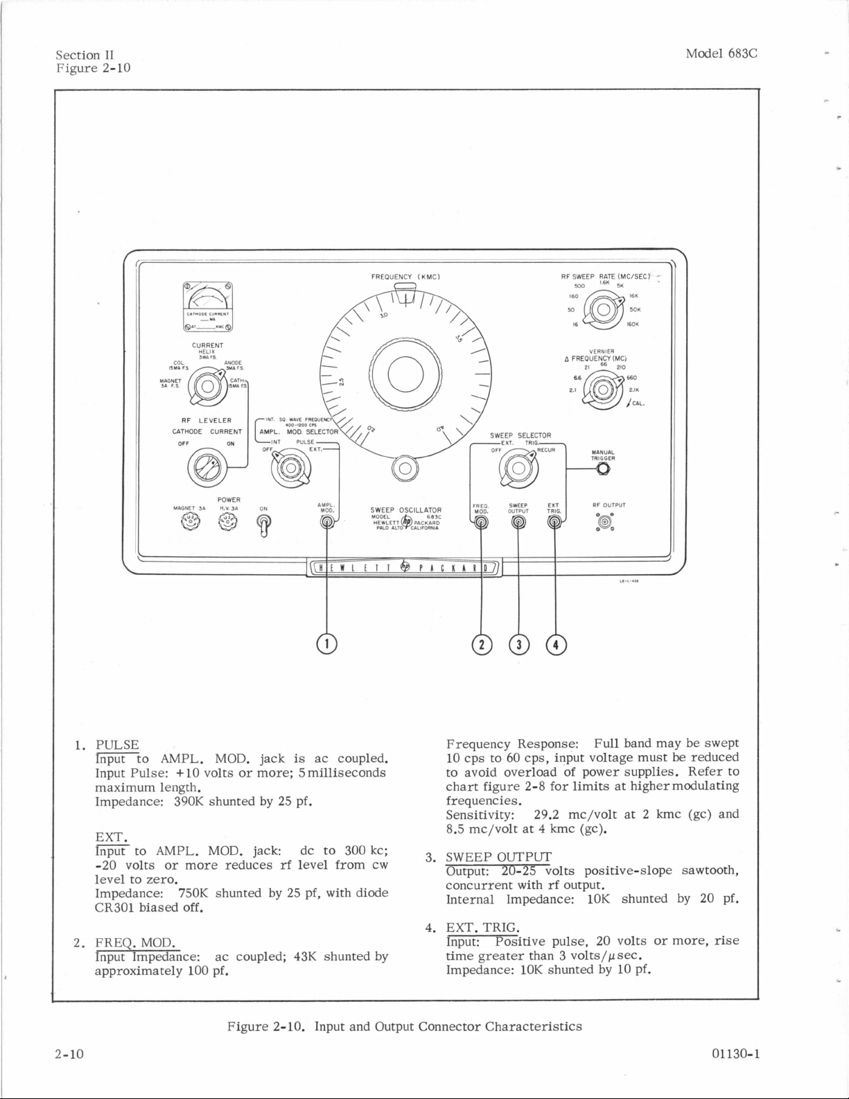
Figure 2-10
I1
Model 683C
.
RF
OUTPUT
s
1.
PULSE
Ixto AMPL. MOD. jack
Input Pulse:
maximum length.
Impedance: 390K shunted by 25 pf.
EXT.
Input
to AMPL. MOD. jack dc
-20 volts
level to zero.
Impedance: 750K shunted by 25 pf, with diode
CR301
2. FREQ. MOD. Input: Positive pulse, 20 volts
Input Impedance:
approximately
+
10
or
more reduces
biased off.
100
volts or more; 5 milliseconds
ac coupled; 43K shunted by
pf.
is
ac coupled.
to
300
rf
level from cw
kc;
Frequency Response: Full band may be swept
10
cps
to
to avoid overload
chart figure 2-8 for limits at higher modulating
frequencies.
Sensitivity: 29.2 mc/volt at 2 kmc (gc) and
8.5 mc/volt at
3.
SWEEPOUTPUT
Output: 20-25 volts positive-slope sawtooth,
concurrent with
Internal Impedance:
4. EXT.TRIG.
time greater than
Impedance: 10K shunted by
60 cps, input voltage must be reduced
of
4
kmc (gc).
rf
output.
3
volts/psec.
power supplies. Refer to
10K
shunted by 20 pf.
10
pf.
or
more,
rise
2-10
Figure 2-
10.
Input and Output Connector Characteristics
01
130-
1
Page 20
Model 683C
Paragraphs 3-1 to 3-2
Section
Ill
SECTION
THEORY
3-1.
CONTENTS.
This section explains how the circuits of the sweep
oscillator operate. First, the overall operation of
the backward-wave osCillator tube
the bwo tube
characteristics of the tube are understood, an overall
picture of the purpose of the various circuits
easily understood.
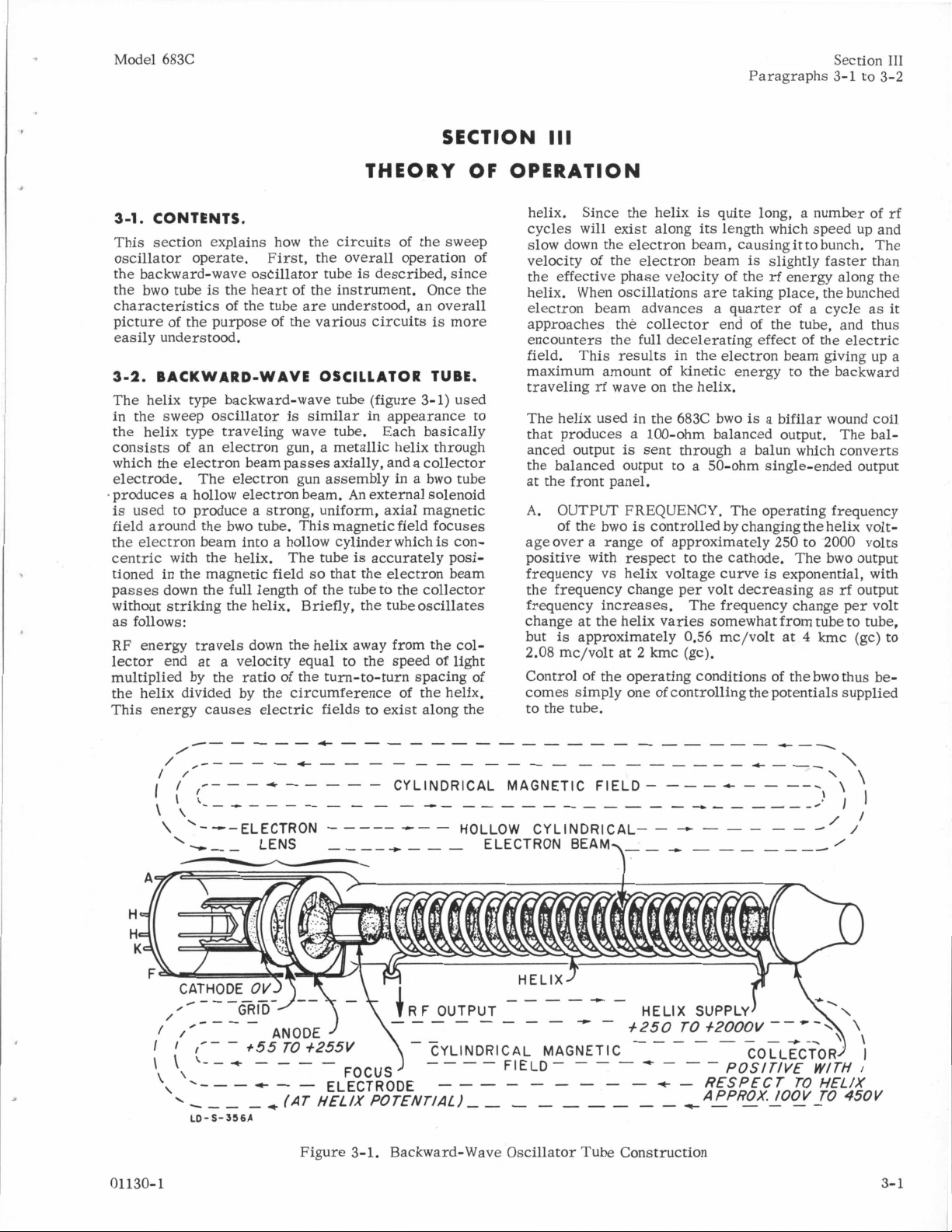
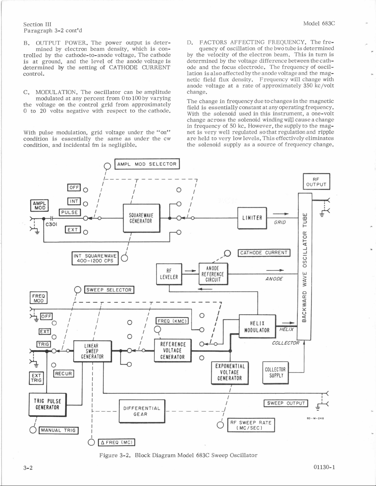
3-2.
BACKWARD-WAVE OSCILLATOR TUBE.
The helix type backward-wave tube (figure 3in
the sweep oscillator
the helix type traveling wave tube, Each basically
consists of an electron gun, a metallic helix through
which the electron beam passes axially, and a collector
electrode. The electron gun assembly
.produces a hollow electron beam.
is
used to produce a strong, uniform, axial magnetic
field around the bwo tube. This magnetic field focuses
the electron beam into a hollow cylinder which
centric with the helix. The tube
tioned
passes down the full length of the tube to the collector
without striking the helix. Briefly, the tube oscillates
as follows:
RF energy travels down the helix away from the
lector end at a velocity equal to the speed of light
multiplied by the ratio of the turn-to-turn spacing of
the helix divided by the circumference of the helix.
This energy causes electric fields to exist along the
is
the heart of the instrument. Once
in
the magnetic field
is
similar
so
is
described, since
the
is
more
1)
used
in
appearance to
in
a bwo tube
An
external solenoid
is
con-
is
accurately posi-
that the electron beam
col-
111
OF
OPERATION
helix. Since the helix
cycles will exist along its length which speed up and
slow down the electron beam, causingit
velocity of the electron beam
the effective phase velocity of the
helix. When oscillations are taking place, the bunched
electron beam advances a quarter of a cycle as it
approaches
encounters the full decelerating effect of the electric
field. This results
maximum amount of kinetic energy to the backward
traveling
The helix used
that produces a 100-ohm balanced output.
anced output
the balanced output to a 50-ohm single-ended output
at the front panel.
A.
OUTPUT FREQUENCY. The operating frequency
of the bwo
ageover a range of approximately 250 to 2000 volts
positive with respect to the cathode.
frequency
the frequency change per volt decreasing as
frequency increases. The frequency change per volt
change at the helix varies somewhat from tube to tube,
but
is
2.08 mc/volt at
Control of the operating conditions of the bwo thus be-
comes simply one of controlling the potentials supplied
to the tube.
is
quite long, a number of
to
is
slightly faster than
rf
the
collector end of the tube, and thus
in
the electron beam giving up a
rf
wave on the helix.
in
the 683C bwo
is
sent through a balun which converts
is
controlled by changing the helix volt-
vs
helix voltage curve
approximately 0.56 mc/volt at 4 kmc (gc) to
2
kmc (gc).
is
a bifilar wound coil
is
bunch. The
energy along the
The bal-
The bwo output
exponential, with
rf
rf
output
01 130-
Figure 3-1. Backward-Wave Oscillator Tube Construction
3-
1
1
Page 21
Section 111
Paragraph 3-2 cont’d
B.
OUTPUT POWER. The power output
mined by electron beam density, which
trolled by the cathode-to-anode voltage. The cathode
is
at
ground, and the level of the anode voltage
determined
control.
C. MODULATION. The oscillator can be amplitude
modulated at any percent from
the voltage on the control grid from approximately
0
to
With pulse modulation, grid voltage under the “on”
condition
condition, and incidental fm
by
the setting of CATHODE CURRENT
0
20 volts negative with respect
is
essentially the same
is
negligible.
AMPL
I
/-----
I
to
as
is
deter-
is
con-
100
by varying
to
the cathode.
under the cw
MOD
SELECTOR
r-------
I
I
is
Model 6836
D.
FACTORS AFFECTING FREQUENCY. The
quency
by the velocity
determined by the voltage difference between the cathode and the focus electrode. The frequency
lation
netic field flux density. Frequency will change with
anode voltage
change.
The change in frequency due
field
With the solenoid used in this instrument,
change
in frequency of
net
is
are
held
the solenoid supply
-7
I
01
of
oscillation
of
the electron beam. This in turn
is
alsoaffected by the anode voltageand the mag-
at
a
is
essentially constant
across
very well regulated
the solenoid winding will cause a change
50
kc. However, the supply
to
very low levels. This effectively eliminates
rate
as
of
the bwo tube
of
approximately
to
changes in the magnetic
at
any operating frequency.
is
to
so
that regulation and ripple
a
source
of frequency change.
determined
350
a
fre-
is
of
oscil-
kc/volt
one-volt
the mag-
.
>I
%
-
w
C301
I\
e.
.,
IEXTIO
Q
ISWEEP
LINEAR
SWEEP
GENE R ATOR GENERATOR
I
I
t
I
SELECTOR
SOUARE WAVE
GENERATOR
i
I
I
I--------
I
LEVELER
VOLTAGE
RF
I
I
“
---c
-
0
LIMITER
0
CATHODE
/
.
ANODE
REFERENCE
CIRCUIT
-1
I
41
EXPONENTIAL COLLECTOR
CURRENT
-
ANODE
I-
I
-W
GRID
1
m
~
3
IY
0
I-
U
-I
J
-
V
v)
0
W
>
4
0
U
a
s
Y
TRIG PULSE
It
GENERATOR
I
3-2
I
I
I
I
Figure 3-2. Block Diagram Model 683C Sweep Oscillator
SWEEP OUTPUT
ED-H-248
01130-1
Page 22
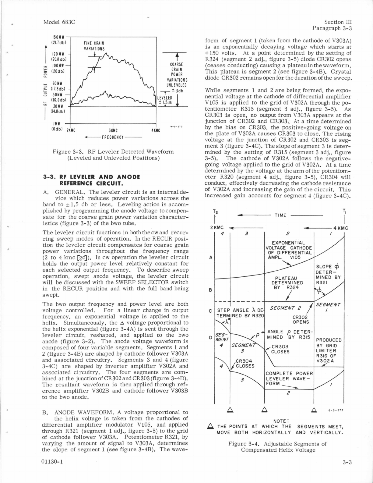
Model 683C
15OWW
(2I.Td b)
w
=
(20db)
0
@-
IWW
(Odb)
Figure 3-3.
3-3.
RF LEVELER
REFERENCE CIRCUIT.
A.
GENERAL. The leveler circuit
vice which reduces power variations across the
band to 1.5 db or
plished by programming the anode voltage to compensate for the coarse grain power variation characteristics (figure 3-3) of the bwo tube.
The leveler circuit functions
ring sweep modes of operation.
tion the leveler circuit compensates for coarse grain
power variations throughout the frequency range
(2 to 4 kmc [gc]).
holds the output power level relatively constant for
each selected output frequency. To describe sweep
operation, swept anode voltage, the
will be discussed with the SWEEP SELECTOR switch
in
the RECUR position and with the
swept.
The bwo output frequency and power level are both
voltage controlled. For a linear change in output
frequency, an exponential voltage
helix. Simultaneously, the
the
helix exponential (figure 3-4A)
leveler circuit, reshaped, and applied to the bwo
anode (figure 3-2). The anode voltage waveform
composed of four variable segments. Segments 1 and
2 (figure 3-4B) are shaped by cathode follower V303A
and associated circuitry. Segments 3 and 4 (figure
3-4C) are shaped by inverter amplifier V302A and
associated circuitry. The four segments are combined at the junction of CR302 and CR303 (figure 3-4D).
The resultant waveform
erence
to the bwo anode.
B. ANODE WAVEFORM.
differential amplifier modulator V105, and applied
through R321 (segment
of cathode follower V303A. Potentiometer R321, by
varying the amount of signal to V303A. determines
the slope of segment
amplifier V302B and cathode follower V303B
the helix voltage
FINE
GRAIN
-+-
Lx
2
1.5db
2KYC 3KWC 4KWC
-FREOUENCY
RF Leveler Detected Waveform
(Leveled and Unleveled Positions)
I
-
AND
ANODE
is
an internal de-
less.
Leveling action
in
both the
In the RECUR posi-
In
cw
operation the
A
voltage proportional to
is
then applied through
A
is
1
voltage proportional to
taken from the cathodes of
1
adj., figure 3-5) to the grid
(see
figure 3-4B). The wave-
leveler
leveler
full
is
is
sent through the
is
cw
and
band being
applied to the
COARSE
GRAIN
POWER
VARIATIONS
UNLEVELED
2
3db
*-I-
273
accom-
recur-
circuit
circuit
is
ref-
Section
Paragraph 3-3
form of segment
is
an exponentially decaying voltage which starts at
+I50 volts.
R324 (segment 2 adj., figure 3-5) diode CR302 opens
(ceases conducting) causing a plateau
This plateau
diode CR302 remains open for the duration of the sweep.
While segments
nential voltage at the cathode of differential amplifier
VI05
is
applied to the grid of V302A through the potentiometer R315 (segment 3 adj., figure 3-5).
CR303
junction of CR302 and CR303.r At a time determined
by the bias on CR303, the positive-going voltage on
the plate of V302A causes CR303 to close. The rising
voltage at the junction of CR302 and CR303
ment
mined by the setting of R315 (segment
3-5). The cathode of V302A follows the negativegoing voltage applied to the grid of V302A. At a time
determined by the voltage at thearm of the potentiom-
eter
conduct, effectively decreasing the cathode resistance
of V302A and increasing the gain of the circuit. This
increased gain accounts for segment
is
open, no output from V303A appears at the
3
(figure 3-4C). The slope of segment
R320 (segment 4 adj., figure 3-5), CR304
i'
2KMC
41
STEP ANGLE
EG-h
VENT
4
SEGMEN
1
(taken from the cathode of V303A)
At
a point determined by
is
segment 2
-
3
/p
1
and 2 are being formed, the expo-
(see
TIME
I
EXPONENTIAL
VOLTAGE CATHODE
OF DIFFERENTIAL
P LATE AU
DETERMINED
BY A324
1
MINED ANGLE
COMPLETE POWER
in
figure 3-4B).
4
-
2
CR302
OPENS
p
BY
DETER- R315
2
the
setting of
the waveform.
3
is
3
adj., figure
(figure 3-4C).
i
SLOPE
DETERMINED BY
SEGMENT
/
PRODUCED
BY GRID
LIMITER
R316 OF
V302A
111
Crystal
As
is
seg-
deter-
will
4
KMC
4
I
A
A
A
THE POINTS AT WHICH THE
MOVE BOTH HORIZONTALLY AND VERTICALLY.
Figure 3-4. Adjustable Segments of
Compensated Helix Voltage
a
NOTE
SEGMENTS MEET,
6-5-217
01130-1
3-3
Page 23
Section 111
Paragraph 3-4
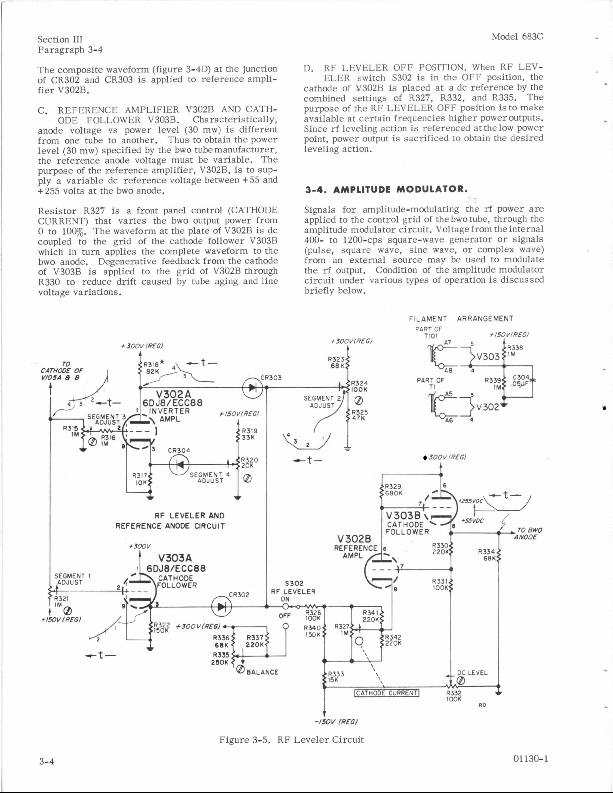
The composite waveform (figure 3-4D) at the junction
of CR302 and CR303 is applied to
fier
V302B.
reference
ampli-
C. REFERENCE AMPLIFIER V302B AND CATH-
ODE FOLLOWER V303B. Characteristically,
anode voltage
vs
power
level
(30 mw)
is
different
from one tube to another. Thus to obtain the power
level (30 mw) specified by
reference
the
purpose of
ply a variable dc
anode voltage must be variable. The
the
reference amplifier, V302B,
reference
the
bwo tubemanufacturer,
is
voltage between
to sup-
+55
and
+255 volts at the bwo anode.
Model 683C
D.
RF LEVELER OFF POSITION. When RF LEVELER switch S302 is in the
cathode of Y302B
is
placed at a dc reference by the
OFF
position, the
combined settings of R327, R332, and R335. The
purpose of the RF LEVELER OFF position
is
to make
available at certain frequencies higher power outputs.
Since
rf
leveling action
point, power output is sacrificed to obtain
is
referenced atthelow power
the
desired
leveling action.
3-4.
AMPLITUDE MODULATOR.
Resistor R327
is
a front panel control (CATHODE
CURRENT) that varies the bwo output power from
0
to 100%. The waveform at the plate of V302B
coupled to
which
the
grid of
in
turn applies the complete waveform to the
the
cathode follower V303B
is
dc
bwo anode. Degenerative feedback from the cathode
of V303B
is
applied to the grid of V302B through
R330 to reduce drift caused by tube aging andline
voltage variations.
i3OOV
(REG)
A
TO
CATHODE
VIOSA
OF
a
B
V302A
R320
20K
Y
RF LEVELER AND
REFERENCE ANODE CIRCUIT
1
Signals for amplitude-modulating the
applied to
the
control grid of the bwo tube, through the
rf
power are
amplitude modulator circuit. Voltage from the internal
400- to 1200-cps square-wave generator or signals
(pulse, square wave,
sine
wave, or complex wave)
from an external source may be used to modulate
the
rf
output. Condition of the amplitude modulator
circuit under various types of operation
is
discussed
briefly below.
FILAMENT ARRANGEMENT
PART
OF
et-
i
300
I33231
68
K
!&a24
V/REG)
IOOK
TI01
300
V
c
A0
(REG1
tl5OVIREG)
t-/
3-4
JEGMENT
JEGMENT
ADJUST
ADJUST
pam
R321
1
IM@
\e/
3V
(REG1
3V
(REG1
1
1
CATHODE
FOLLOW
E R
S302
?F
-CR302
vu
BALANCE
Figure 3-5. RF Leveler Circuit
Figure 3-5. RF Leveler Circuit
LEVEL.ER
ON
R333
15K
-fx)V
-fx)V
(REG)
(REG)
"?"
\
\
\
\
ICATHODE
ICATHODE
CURRENT]
CURRENT]
R331
IOOK
R332
R332
IOOK
IOOK
..
RO
RO
01130-1
Page 24
Model 683C
A.
CW
OPERATION.
In
cw operation (AMPL.
MOD.
SELECTOR at OFF) diode CR301 clamps the bwo
control grid to ground. The
mined by the voltage on
rf
output level
the
anode, which
is
is
adjusted
deter-
by means of the CATHODE CURRENT control.
B.
INTERNAL SQUARE-WAVE OPERATION. With
the AMPL.
MOD.
SELECTOR on INT dual triode
V301 operates as a symmetrical free-running multivibrator. The frequency
mined
by
the charge and discharge time of C302 and
of
the
square wave
is
deter-
series-connected R303 and R302 (INT. SQ. WAVE FREQUENCY control). The symmetry of
is
set by adjusting (with
R3lO)
the
square wave
the dc bias on the
B
section of V301. The two adjustments are slightly
interdependent. The square-wave amplitude
is
clamped
to ground through crystal diode CR301. Thus the level
of the
rf
output during the “on”portionof the squarewave cycle corresponds to the cw level, set by the
CATHODE CURRENT control.
Paragraphs 3-5 to 3-6
Section
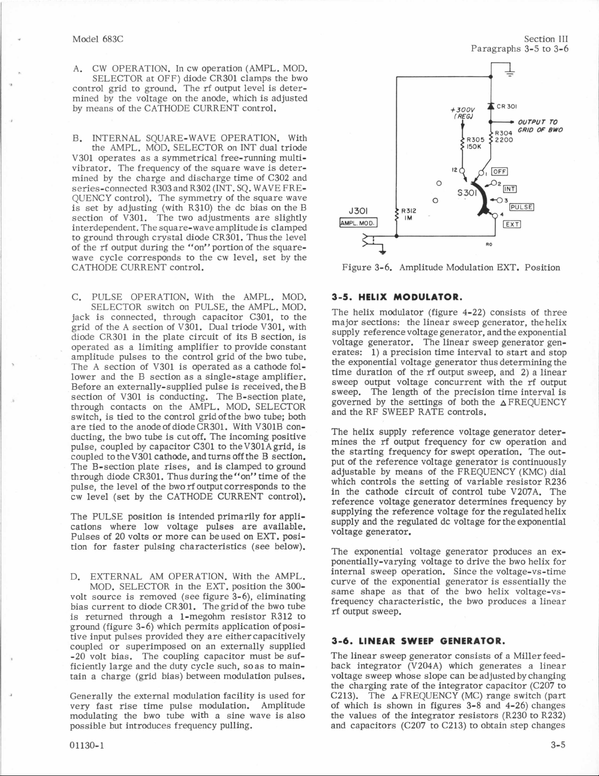
OUTPU
r
OF
TO
BWO
’5
R304
GRID
-
RO
Figure 3-6. Amplitude Modulation EXT. Position
Ill
C. PULSE OPERATION. With the AMPL.
SELECTOR switch on PULSE, the AMPL.
jack
is
connected, through capacitor C301, to the
grid of the
diode CR301
A
section of V301. Dual triode V301,
in
the plate circuit of
its
B
MOD.
MOD.
with
section,
is
operated as a limiting amplifier to provide constant
amplitude pulses to the control grid of the bwo tube.
The
A
section of V301
lower and the
B
Before an externally-supplied pulse
section of V301
is
through contacts on the AMPL.
switch,
is
tied to the control grid of the bwo tube; both
is
operated as a cathode fol-
section as a single-stage amplifier.
is
received,
the
conducting. The B-section plate,
MOD.
SELECTOR
are tied to the anode of diode CR301. With V301B conducting, the bwo tube
pulse, coupled by capacitor C301 to theV301Agrid,
is
cut off. The incoming positive
is
coupled to theV301 cathode, and turns off the B section.
The B-section plate rises, and
is
clamped
to
ground
through diode CR301. Thus during the “on” time of the
pulse, the level of the bwo
rf
output corresponds to the
cw level (set by the CATHODE CURRENT control).
The PULSE position
is
intended primarily
for
applications where low voltage pulses are available.
Pulses of
tion for faster pulsing characteristics
D.
volt source
20
volts or more can beused on EXT. posi-
EXTERNAL
MOD.
SELECTOR
is
(see
below).
AM
OPERATION. With the AMPL.
in
the Em. position the 300-
removed (see figure 3-6), eliminating
bias current to diode CR301. Thegridof the bwo tube
is
returned through a 1-megohm resistor R312 to
ground (figure 3-6) which permits application of posi-
tive input pulses provided
they
are either capacitively
coupled or superimposed on an externally supplied
-20
volt bias. The coupling capacitor must be
sufficiently large and the duty cycle such, soas to maintain a charge (grid bias) between modulation pulses.
Generally
very fast
modulating the bwo tube with a sine wave
the
external modulation facility
rise
time pulse modulation. Amplitude
is
used for
is
also
possible but introduces frequency pulling.
B
3-5.
HELIX MODULATOR.
The helix modulator (figure 4-22) consists of three
major sections:
the
linear sweep generator, the helix
supply reference voltage generator, and the exponential
voltage generator. The linear sweep generator generates:
1)
a precision time interval to start and stop
the exponential voltage generator thus determining the
time duration of the
sweep output voltage concurrent with the
sweep. The length of the precision time interval
rf
output sweep, and
2)
a linear
rf
output
is
governed by the settings of both the AFREQUENCY
and the RF SWEEP RATE controls.
The helix supply reference voltage generator determines the
rf
output frequency for cw operation and
the starting frequency for swept operation. The output of the reference voltage generator
adjustable by means of the FREQUENCY
which controls the setting
in
the cathode circuit of control tube V207A. The
of
variable resistor R236
is
continuously
(KMC)
dial
reference voltage generator determines frequency by
supplying the reference voltage for the regulated helix
supply and the regulated dc voltage for the exponential
voltage generator.
The exponential voltage generator produces an exponentially-varying voltage to drive the bwo helix for
internal sweep operation. Since the voltage-vs-time
curve
of the exponential generator
is
essentially
the
same shape as that of the bwo helix voltage-vsfrequency characteristic, the bwo produces a linear
rf
output sweep.
3-6.
LINEAR SWEEP GENERATOR.
The linear sweep generator consists of a Miller feed-
back integrator (V204A) which generates a linear
voltage sweep whose slope can be adjusted by changing
the charging rate
of
the integrator capacitor ((2207 to
C213). The AFREQUENCY (MC) range switch (part
of which
is
shown in figures 3-8 and 4-26) changes
the values of the integrator resistors (R230 to R232)
and capacitors (C207 to (2213) to obtain step changes
01130-1
3-5
Page 25
Section
Figure
111
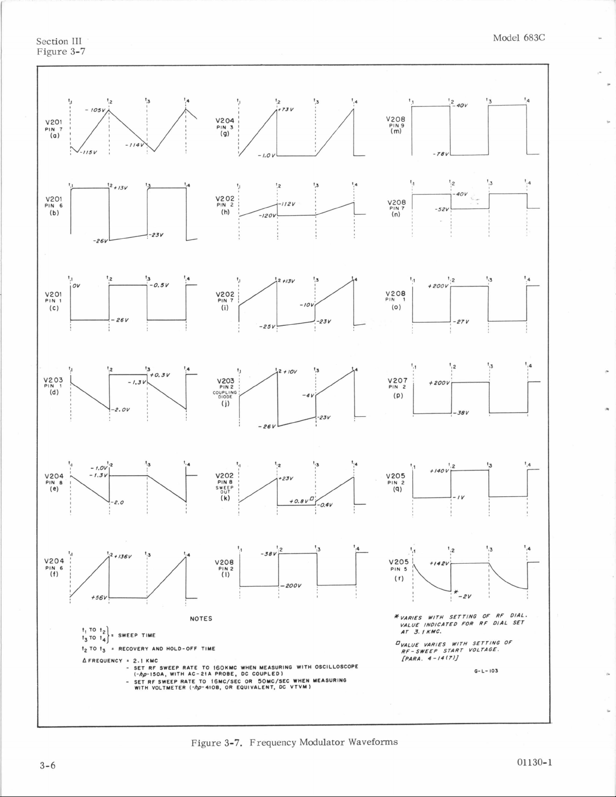
3-7
Model
683C
:N
I I !
v201
PIN
7
(0)
I
:
-1I5V
v201
PIN
1
(C)
I
;
-I14V,
'J
I
I
V208
PIN
9
(
rn)
s2-40v
V208
v202
I
PIN
7
DIODE
I
I
-25V.
-1ov'
,-23V
V204
PIN
(e)
3-6
8
;
I
t3T0
tt
fpTO
A
.-2.0
14
=
SWEEP TIME
lz1
15
RECOVERY AN0 HOLD-OFF TIME
FREOUENCY
,
NOTES
2.
I
KMC
-
SET RF SWEEP RATE
(-bp150A, WITH AC-2tA PROBE, DC COUPLED)
-
SET RF SWEEP RATE
WITH
VOLTMETER
TO
t6OKMC WHEN YEASURING WITH OSCILLOSCOPE
TO
16YC/SEC
(-hp-4lOB,
Figure
OR
OR
3-7.
SOMC/SEC WHEN MEASURlNO
EQUIVALENT, OC
Frequency Modulator
VTVM)
Waveforms
*VARIES
a~~~~~
WITH
f
KMC.
VARIES
4 - I4
SETTING
FOR
WITH
171J
RF
SETTING OF
G- L-
VALUE INDICATED
Ar
3.
RF-SWEEP START VOLTAGE.
[PARA.
OF
RF
DIAL
103
DIAL.
SET
01
130-
1
Page 26
Model 683C
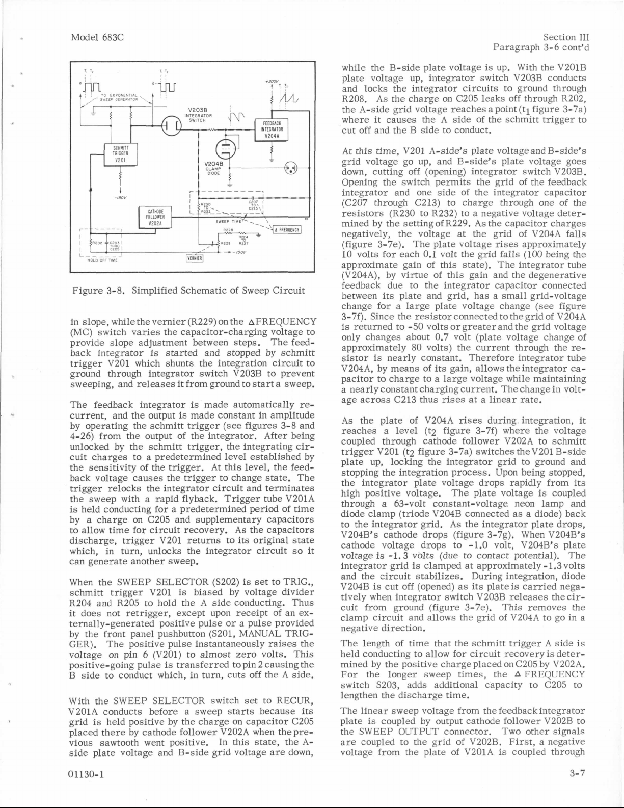
Paragraph 3-6 cont’d
Section
I11
Figure 3-8. Simplified Schematic of Sweep Circuit
in slope, while the
(MC) switch varies the capacitor-charging voltage to
provide slope adjustment between steps. The feedback integrator
trigger V201 which shunts the integration circuit to
ground through integrator switch V203B to prevent
sweeping, and releases
The feedback integrator
current, and the output
by operating the schmitt trigger
4-26) from the output of the integrator. After being
unlocked by the schmitt trigger, the integrating
cuit charges to a predetermined level established by
the sensitivity of the trigger.
back voltage causes the trigger to change state. The
trigger relocks the integrator circuit and terminates
the sweep with a rapid flyback. Trigger tube V201A
is
held conducting for a predetermined period of time
by a charge on C205 and supplementary capacitors
to allow time for circuit recovery.
discharge, trigger V201 returns to
which, in turn, unlocks the integrator circuit
can generate another sweep,
When the SWEEP SELECTOR (S202)
schmitt trigger V201
R204 and R205 to hold the
it does not retrigger, except upon receipt of an externally-generated positive pulse or a pulse provided
by the front panel pushbutton (S201, MANUAL TRIGGER). The positive pulse instantaneously raises the
voltage
positive-going pulse
B side to conduct which, in turn, cuts off the
With the SWEEP SELECTOR switch set to RECUR,
V201A conducts before a sweep starts because
grid
placed there by cathode follower V202A when theprevious sawtooth went positive. In this state, the
side plate voltage and B-side grid voltage are down,
on
is
held positive by the charge on capacitor C205
vernier
is
pin 6 (V201) to almost zero volts.
(R229) on the AFREQUENCY
started and stopped by schmitt
it
from ground to start a sweep.
is
made automatically
is
made constant in amplitude
(see
figures 3-8 and
At
this level, the feed-
As
the capacitors
its
original state
is
set to TRIG.,
is
biased by voltage divider
A
side conducting. Thus
is
transferred to pin 2 causing the
A
re-
cir-
so
This
side.
its
A-
it
while the B-side plate voltage
plate voltage up, integrator switch V203B conducts
and locks the integrator circuits to ground through
R208.
the A-side grid voltage reaches a point
where it causes the
cut off and the B side to conduct.
At this time, V201 A-side’s plate voltageand B-side’s
grid voltage go up, and B-side’s plate voltage goes
down, cutting off (opening) integrator switch V203B.
Opening the switch permits the grid of the feedback
integrator and one side of the integrator capacitor
(C207 through C213) to charge through one
resistors (R230 to R232) to a negative voltage determined by the setting of R229.
negatively, the voltage at the grid of V204A falls
(figure 3-7e). The plate voltage
10 volts for each 0.1 volt the grid falls (100 being
approximate gain of this state). The integrator tube
(V204A), by virtue of this gain and the degenerative
feedback due to the integrator capacitor connected
between its plate and grid, has a small grid-voltage
change for a large plate voltage change
3-7f). Since the resistor connected to the grid of V204A
is
only changes about 0.7 volt (plate voltage change of
approximately
sistor
V204A, by means of its gain, allows the integrator capacitor to charge to a large voltage while maintaining
a nearly constant charging current. The change in voltage across C213 thus
As
reaches a level (t2 figure 3-7f) where the voltage
coupled through cathode follower V202A to schmitt
trigger V201 (t2 figure 3-7a) switches theV201 B-side
plate up, locking the integrator grid to ground and
stopping the integration process. Upon being stopped,
the integrator plate voltage drops rapidly from
high positive voltage. The plate voltage
through a 63-volt constant-voltage neon lamp and
diode clamp (triode V204B connected as a diode) back
to the integrator grid.
V204B’s cathode drops (figure 3-7g). When V204B’s
cathode voltage drops to -1.0 volt, V204B’s plate
voltage
integrator grid
and the circuit stabilizes. During integration, diode
V204B
tively when integrator switch V203B releases the
cuit from ground (figure 3-7e). This removes the
clamp
negative direction.
The length of time that the schmitt trigger
held conducting to allow for circuit recovery
mined by the positive charge placed on C205 by V202A.
For the longer sweep times, the
switch S203, adds additional capacity to C205 to
lengthen the discharge time.
The linear sweep voltage from the feedback integrator
pl.ate
the SWEEP OUTPUT connector. Two other signals
are coupled to the grid of V202B. First, a negative
voltage from the plate of V201A
As
the charge on C205 leaks off through R202,
A
side of the schmitt trigger to
returned to -50 volts orgreaterand the grid voltage
80
volts) the current through the
is
nearly constant. Therefore integrator tube
rises
the plate of V204A
As
is
-1.3 volts (due to contact potential). The
is
clamped at approximately
is
cut
off
(opened) as
circuit
is
and allows the grid of V204A to go in a
coupled by output cathode follower V202B to
is
up. With the V201B
(ti
figure 3-7a)
of
As
the capacitor charges
rises
approximately
(see
figure
at a linear rate.
rises
during integration, it
is
coupled
the integrator plate drops,
-
1.3
volts
its
plateis carried nega-
A
side
is
deter-
A
FREQUENCY
is
coupled through
the
the
re-
its
cir-
is
0
1130- 1
3-
7
Page 27

Section
111
Paragraph 3-7
diode V203A to cut off V202B during thefly-back time
and at all times before a sweep starts
3-7j). Second, a dc voltage
by R217 which
output from 5203
will
give an instantaneous +1.5 volt
when
is
applied and adjusted
schmitt trigger V201 flips and
(see
figure
opens coupling diode V203A removing the negative
bias on
the
grid of V202B
(see
figure 3-7k). The
instantaneous initial positive output voltage produces
a thin section of trace on
the
cathode ray tube which
separates the beginning of the main trace from the
bright dot, or vertical line, which occurs during
circuit recovery time.
Model 683C
3-7.
HELIX SUPPLY REFERENCE VOLTAGE AND
EXPONENTIAL VOLTAGE GENERATORS.
The frequency of the
rf
output of the sweep oscillator
is determined by the amplitude of the voltage applied
to the bwo helix. The amplitude of the helix voltage
is
varied by varying the
to the regulated helix supply (figure 4-22).
operation, the
reference
reference
voltage supplied
For
voltage, supplied by the
cw
reference voltage generator, has a constant amplitude,
the level being set by means of the FREQUENCY
(KMC) dial. For sweep operation, the referencevoltage
is
supplied by the exponential voltage generator.
The amplitude of this voltage starts at a value estab-
lished by the setting of the FREQUENCY (KMC) dial,
and then decreases exponentially. The resulting output
is
a linear
device. Operation of the
rf
sweep, the bwo beingan exponential-law
reference
and exponential
voltage generators are briefly described below.
A.
REFERENCE VOLTAGE GENERATOR. Basic-
ally, the reference voltage generator (figures
3-9 and 4-26)
source of
is
reference
a typical voltage regulator with a
voltage (regulator tube V206), a
control tube (V207A) which compares the reference
voltage with a sample of the reference voltage generator output, and a
series
regulator (V207B). A signal
from the control tube controls conduction through the
series regulator
of the output to deviate from thedesiredlevel
in
such manner that any tendency
is
com-
pensated for.
The output of V207B
switch V205A and applied
is
brought through regulator
1)
to differential amplifier
V105 in the regulated helix supply (figure 4-22) and
capacitor C215
(in
the
line
to VlOS), and
2)
to the
grid of control tube V207A to provide the sample of
output voltage required by the regulator. Status of
tubes during
However, the
cw
operation
reference
is
shown in table 3-1.
voltage generator’s output
level can be varied from the front panel providing
the means for selecting the frequency of the
In addition,
reference
it
is
possible to electronically turn off the
voltage generator and to turn it on again
rf
output.
after precise predetermined time intervals required
for sweep operation. The circuit sequences which
effect this action are described in subparagraph B.
B. EXPONENTIAL VOLTAGE GENERATOR. Oper-
ation of
all the
rent for charging the capacitance
the
circuits
exponential voltage generator requires
shown in figures 3-9 and 4-26. Cur-
in
the
rc
circuit
I
[FREOUENCV IXHCI]
I,
Figure 3-9. Simplified Schematic of
Exponential Sweep Circuit
is
of the exponential voltage generator
reference
voltage generator
citor(
resistor network, and it
voltage which
Turn-off of the
voltage generator.
is
turned off, the charged capa-
s)
starts to discharge through
is
this exponentially decaying
is
fed to the regulated helix supply.
reference
voltage generator (as
As
supplied by the
soon as the reference
its
corresponding
well
as its turn-on after a precise predetermined time)
under the control of the linear sweep time generator.
The rate at which the capacitor discharges (and thus
the rate at which the
rf
frequency
is
changing)
determined by the values of capacitance and resistance
selected by the RF SWEEP RATE (MC/SEC) switch,
S204. The exponential voltage generator
when the reference voltage generator
on by
voltage
the
linear sweep time circuit. How long the
is
permitted to decay
is
thus determined by
the linear sweep time circuit which
is
turned off
is
again turned
is
controlled by
AFREQUENCY (MC) switch S203. Thus the width
of band swept (band “distance”) (sweep time x sweep
rate)
is
S204. (The
though
action
In the following discussion of
“sweep”
the linear sweep time generator; the term
refers
Operation of the linear sweep time generator
determined by the settings of both S203 and
A
FREQUENCY switch determines time
it
is
calibrated in terms of “distance”.) Circuit
is
discussed in more detail below.
refers
circuit
to the sawtooth voltage produced by
action the term
“rf
sweep”
to the output of the bwo tube (figure 4-21).
is
de-
scribed in paragraph 3-6, and only that part of the
action which
is
pertinent to an understanding of the
exponential voltage generator will be discussed here.
Condition of main tubes at various stages of circuit
action
is
shown
in
table 3-1.
With the instrument set for internal sweep operation,
the linear sweep time generator
is
producing a sawtooth voltage. While the voltage at the output of feedback integrator V204A
schmitt trigger V201
conducting. Feedback from V204A
is
rising, the A section of
is
cut off and the B section
is
returned to the
is
grid of V201A, and when the amplitude of the sawtooth
reaches
V201 changes state: the
and the B section
the
schmitt trigger upper hysteresis limit,
A
section starts to conduct
cuts
off. Thefeedback also charges
is
is
3-8
01 130-
1
Page 28

Model 683C
Table
3-1.
Condition of Tubes During CW and RF Sweep
Section 111
Paragraph 3-7 cont’d
Oper-
ation
State of Circuit
cw
RF
Sweep
capacitor C205 in the V201A grid circuit, and this
charge holds V201A conducting during the sawtooth
dead time.
With V201A conducting there
the grid of V207B, supplied through V208A; this holds
series
cut off, the cathode of regulator switch V205A
pulled in a negative direction, holding V205A in conduction. In the same manner
current through V207B, diode CR204, and V205A
establishes the charge on capacitor C215 at a level
which corresponds to the setting
(KMC) dial.
During the sawtooth dead time, the charge on capacitor
C205 leaks off through resistor R202. When the
voltage across C205 drops to the schmitt trigger
hysteresis limit, V201 again changes state: V201A
cuts
tive signal on the V207B grid, cutting off conduction
through the
switch V205A and 2) closes clamp V205B. With
supply voltage removed, capacitor C215 starts
discharge through the resistors selected by the RF
SWEEP RATE switch. Thus the voltage applied
V105 in the regulated helix supply starts to fall exponentially, causing the frequency
change at the rate selected by the
switch. The
on the slider of variable
linearity adjustment.
In the
the amplitude
the schmitt trigger upper hysteresis level, and conducting V201A turns on the reference voltage generator.
To protect the bwo tube, however, circuitry
cluded
a level. The clamp V205B, when conducting, holds
the plate of V205A at approximately
the linear sweep time generator does not turn on the
reference voltage generator before the exponential
voltage decays to approximately
will start to conduct and will clamp the exponentiallydecaying voltage to
Before
Exp Gen capacitors charging
RF sweep starts; Ref Volts
Gen turned
RF sweep reaches low end:
regulator V207B in conduction. With V201B
off and V201B turns on. This results in a nega-
usual
to
prevent the voltage from decaying to
rf
sweep starts;
off
schmitt trigger trips
decaying voltage reaches
-1.1
Cond.
series
or
volt
=
conducting
is
a positive signal on
as
in
of
the FREQUENCY
regulator which 1) opens regulator
of
the
RF
rc
network discharges toward the potential
resistor
case the voltage decay
of
the sawtooth voltage again reaches
-1.1
volts.
R244, the
will
-1.1
V201A
Cond.
Cond.
c.
0.
Cond.
is
cw
operation,
lower
to
to
rf
sweep to
SWEEP RATE
rf
sweep
continue until
is
in-
too
low
-1.1
volts.
volts, V205A
If
V201B
c.
0.
c.
0.
C.
0.
Cond.
Cond.
Cond.
V205A
Cond.
Cond.
I
Cond.
c.
Cond.
Cond.
C.
0.
0.
Cond.
Thus the length of time the voltage decayis permitted
to continue (unless it reaches
mined by how long the
V201 (and therefore the reference voltage generator)
is
cut off. This period
amplitude
tive value. This total time
nents switched into the linear sweep time generator
circuit by the AFREQUENCY switch (S203).
The voltage at the center tap
established by current distributed through
R233, R234, R263, R240, diode CR202, and the
section of V201. In
diode CR202
R233 and R263
the junction
Resistor R263 establishes the voltage at the cathode
of
coupling diode V203A at such level that V203A will
not close until V201A starts to conduct (when the sawtooth reaches maximum level and the flyback starts).
Tap resistors R234 and R240 change the voltage char-
acteristic
that dial calibration
frequency end
Diode CR204
tains
a
cathode of V207B and the plate
Front panel controls
RF SWEEP RATE (MC/SEC), S204, are operated
through differential gears, and are
a combination which would require a sweep time
less
than 0.0135 second
the
A
FREQUENCY selector
S203, the
switch S204
for
too high a rate
the same manner, the RF SWEEP RATE selector
operate switch S203
set
for too short a sweeptime(toonarrow a frequency
for
band)
0.
C.
Cond.
C.
0.
c.
of
the sawtooth to reach
of
of
the V207A cathode circuit in such manner
is
55-volt difference in potential between the
A
FREQUENCY selector
if
the sweep rate selected.
cut off
0.
-1.1
A
section
is
the time required
is
determined by compo-
of
potentiometer R236
cw
operation (V201A conducting),
is
forward-biased and the junction of
is
practically at ground, CR202 clamps
R233 and R263
is
improved (crowding at the low-
is
reduced).
a 55-volt breakdown diode which main-
A
the RF SWEEP RATE selector
for
if
so
of
FREQUENCY (MC), S203, and
is
prevented. Thus, though
is
the control
the sweep band selected. In
the A FREQUENCY switch
C.
Cond.
Cond.
-
volts first)
of
schmitt trigger
its
maximum posi-
it cannot go negative.
V205A.
so
arranged that
will
V205B
C.
0.
C.
0.
Cond.
0.
0.
C.
Cond.
is
deter-
for
the
is
resistors
of
for
switch
also operate
is
set
will
is
A
0
1130-
1
3-9
Page 29

Section 111
Paragraph 3-8
Model 683C
3-8.
REGULATED POWER SUPPLIES.
In
addition to the magnet regulated power supply,
are
five
1) the regulated -150 volt supply which
regulated voltages generated in the 683C:
is
not dependent
there
upon any other supply but affects all other supplies,
2) the regulated, +300 volt supply which depends upon
the
-150 volt supply for a
reference
voltage,
3)
the
regulated helix supply which depends upon both the
-150 volt and +300 volt supplies, 4) the collector
supply which depends upon the regulated helix supply
to determine its output voltage, and 5) a
reference
voltage supply (helix supply reference voltage gen-
erator)
reference
tors are fed by half-wave silicon
in
the frequency modulator, which provides a
for the regulated helix supply. The regula-
rectifiers
powered
from a single power transformer, T101.
The sequence of operation upon applying
line
power to
the 683C and the operation of the helix overload relay
are explained on the magnet power supply voltage and
resistance diagram (figure 4-15).
The operation of all the voltage regulators
so
only the operation of the -150 volt regulator
is
similar,
is
explained.
A.
-150 VOLT REGULATED POWER SUPPLY. In
the -150 volt regulated supply (figure4-21), CR105
and CR106
approximately 420 volts to the regulator
V107B. Since the output voltage
spect to ground the cathode of V107B
The grid-to-cathode voltage of V107B
class
variable resistor which adjusts
are
half-wave rectifiers which supply
is
negative with
is
is
A
operating conditions, and the tube acts
its
resistance tomain-
series
tube,
re-
grounded.
adjusted to
like
a
tain a constant voltage on the -150 volt bus. Thus at
normal
line
voltage, the tube has approximately
270 volts drop from plate to cathode.
V108, a glow discharge
constant voltage difference between
reference
tube, maintains a
-
150 volts and the
grid of the differential amplifier control tube, V109.
The cathode of the triode section
will
maintain a constant 1-volt difference with the grid potential and thus
keeps a constant 89-volt difference between the -150
volt bus and the cathode of the pentode section. Voltage divider R147, R148, and R149 provides theproper
fraction of the -150 volts for the control grid of the
pentode section. R148 adjusts the exact value of the
bias
so
that the voltage at the grid of
series
tube
V107B is held at the correct value. If the -150 volt
bus tries to increase toward -151 volts, the increase
will
also make the control grid (pin
2)
of V109 go in a
positive direction with respect to the cathode. (The
cathode
is
held at a constant voltage with respect to
the -150 volt bus by the reference tube, V108, and
the cathode follower triode section in V109.) The
positive-going grid (pin 2) causes increased plate
current to flow through the pentode section and R146.
This causes increased voltage drop across R146 which
lowers the grid voltage on V107B. The increased
resistance of V107B brings the bus voltage back toward -150 volts.
crease, the process
If
-150 volt level tends to de-
the
is
the same but in the reverse
direction.
C123 is a coupling capacitor which couples ac ripple
directly to the grid of the control tube which in turn
acts to regulate it out of the output
as a dc change. This results
ripple voltage
in
the regulated output.
in
the same manner
in
very low values of
B. +300 VOLT REGULATED SUPPLY. The300-volt
supply circuit is similar to that of the -150 volt
supply except
it
is
referenced to - 150 volts and includes
a ripple compensating voltage divider (R137 and R138)
from the unregulated output to ground. The voltage
tap-off from the divider
of V107A
this arrangement
(see
figure 4-22). Compensating action of
is
is
applied to
described below.
the
screen
grid
C. REGULATED HELIX SUPPLY. Screen voltage for
control tube V103
is
supplied from its unregulated source, through
in
the regulated helix supply also
dividers R115-R119. With this arrangement of the
control tube
lation for changes
screen
circuit, there
in
line
voltage. Circuit action
is
improved regu-
is
similar to that which occurs with a changing voltage
on
the
grid of the control tube: a change in screen
voltage
tube in such direction that a change in
be compensated for by the
sult
over the range of 103 to 127 volts line voltage.
results
is
an extremely constant output voltage regulation
in
a change
in
conduction through the
line
series
regulator. The
voltage
will
re-
In
addition, ripple voltage in the unregulated source drives
the
screen
in
the proper direction to help regulate
ripple out of the output, further reducing the ripple
level.
Operation of the regulated helix supply
that of the low voltage supplies. However, it
is
similar to
is
more
elaborate due to the extreme range of voltage control
necessary, and because modulating voltages must be
introduced. The voltage control tubes,
(series
regulators), require the single-ended ampli-
VlOl
andV102
fier, V103, driven by a differential amplifier, V105,
which serves two other purposes
helix waveform
applied to the
is
taken at the cathode of V105 and
rf
leveler circuit 2) externally-supplied
1)
the exponential
modulation voltages from the FREQ. MOD. jack are
fed to the grid of V105 to vary the helix voltage, thus
varying
the
frequency. Since two different helix modulating signals must also be applied to the voltage regulator, and
since
a greater order of regulation
is
necessary for helix operation, two stages of voltage amplification are used to obtain greater gain and bandwidth.
The
reference
is
obtained from the helix supply
generator in the frequency modulator, and
to one side of differential amplifier V105.
voltage for the regulated helix supply
reference
voltage
is
applied
A
sample
voltage from the regulated helix supply output and a
calibrating voltage obtained from voltage divider stick
R132, R133, R134, and R135 are fed to the other grid
of the differential amplifier. The calibrating voltage
divider stick contains potentiometers which set the
upper and lower helix voltage limits and, in turn, the
upper and lower
sweep voltages, which produce the
controlled exponential decays in the regulated
rf
output frequency limits. The
rf
swept output, are
refer-
ence voltage obtained from the frequency modulator.
.
c
3-10
01 130-
1
Page 30

Model 683C
Section
Paragraph 3-9
111
The sample voltage from the regulator output
through a frequency-compensated divider composed
of R122, 154, 150, 151, C114, and R131 through
R135, C116, C117. Coupling from the plates of differential amplifier V105 to voltage control tube V103
is
through divider V110, R128, R127 to obtain the
correct dc voltage level for
these compensated coupling networks and the frequency-compensation network
V103 serve to control the gain
lator feedback loop
impedance of the supply remains constant at
over the required frequency range.
The collector supply
tor tubes, V102A and
ages from a divider powered by the regulated helix
voltage. The purpose of the collector
is
to keep the voltage between the collector and helix
within
series to handle the maximum voltage that can occur,
which
3-9.
The backward-wave tube requires a powerful axial
magnetic field to hold its hollow electron beam
focus throughout the full length
netic field must be ripple-free and very constant. To
this end, the magnet power supply
and maintains an exact magnetic field in spite of line
voltage variations and temperature variations which
change the dc resistance of the solenoid. To accomplish current regulation, a two-stage differential
amplifier senses a voltage which
the magnet current and compares it against a stable
reference voltage. The differential amplifier, upon
sensing any change
the internal resistance of tubes
magnet, and holds the magnet current constant.
V1
(resistances), while
ential amplifier which senses any change
drop across voltage divider stick R29, R30, R31. V3,
operated from its own dc power source, provides a
stable dc reference voltage against which the sampled
voltage
regulators serve to carry a portion
acceptable limits. Two tubes are required
is
about 1800 volts.
MAGNET CURRENT SUPPLY (REGULATED).
and
V2
(figure 4-20) are the
is
compared. Resistors shunting the
in
such a manner that
is
B
in
V4
the
grid of V103. All of
in
the cathode circuit of
in
each step of the
composed of two series regula-
in
series, controlled by volt-
series
of
the helix. The mag-
is
current regulated
is
proportional to
the magnet current, controls
in
series with the
series
and V5
is
a two-state differ-
of
the
is
the
internal
12
regulators
regulators
in
the voltage
series
0.7
ampere
fed
regu-
ohms
in
in
required by
have parasitic suppressor resistors while the cathodes
have current equalizing resistors.
The dc for the magnet supply
age-doubler circuit which operates directly from
power line. One
in
series with one of the filament windings of T101. This
winding
voltage going to the silicon rectifier voltage doubler.
When the instrument
tion, the voltage doubler
from one half of the primary 'of power transformer
T1 which
motor and the high-voltage transformer are operated
from the other half of the transformer to minimize
unbalanced load on the two halves of the primary
winding.
the
is
poled
is
acting as a,
magnet. Grids of
wire
of the power source
so
that it adds 6 volts to the supply
is
connected for 230-volt opera-
2:
1
the
series regulators
is
obtained from a volt-
is
is
supplied with 115 volts
autotransformer. The fan
the
connected
the
WARNING
Be extremely careful when working
magnet power-supply section since many tube
socket terminals, filter electrolytic capacitor
terminals and cans, etc. are directly connected to the power line. The instrument
chassis
prong connector.
by a test probe etc. will cause a direct short
circuit on
currents that will
fuses can blow, may severely damage the
strument. The magnet supply ground
floating and
in
This voltage-doubler circuit
nate an additional bulky power transformer.
The magnet circuitry
rest of the instrument, and
is
which are connected to the power line are
exposed. The polarities of the grounded and
ungrounded power conductors have been carefully controlled.
a properly connected three-prong grounded
receptacle, polarity will be maintained as
intended. For
that a three-prong to two-prong adapter not
be used with this instrument.
is
grounded through the NEMA three-
An
accidental short caused
the
power line. The high fault
flow,
before the instrument
is
not related to any other ground
the instrument.
is
used to elimi-
is
separate from the
the
such that a minimum number of points
If
the instrument
this
reason, it
is
recommended
in
the
in-
is
parts layout
is
used with
01130-1
3-11/3-12
Page 31

Model
683C
Paragraphs
Section
4-1
to
IV
4-2
SECTION
MAINTENANCE
4-1.
GENERAL.
This section contains information on the maintenance
and repair of the sweep oscillator.
A
suggested quick-check procedure
fying that the instrument
check
is
made with the instrument in its cabinet. The
procedure
schedule is set up to verify instrument performance,
where incoming quality control checks instrument
operation, or where the operator wishes to quickly
satisfy himself that the instrument
mally and
A
troubleshooting chart systematically follows a
logical check sequence through the instrument and
indicates which adjustments must be rechecked after
repairing any particular circuit.
A
complete
adjustment of all
The specifications for the sweep oscillator are given
in
the front of this manual.
additional data for your convenience in analyzing
performance. These tests and data are not to be considered as specifications.
Wherever possible, standard components are used
the manufacture of Hewlett-Packard instruments.
Your local Hewlett-Packard sales office
source for special spare or replacement parts; they
maintain a parts stock for your convenience. When
ordering parts, please specify instrument model and
serial number plus the component description and stock
number as
Parts (section
Your local Hewlett-Packard sales office also maintains
complete facilities and specially trained personnel to
assist you with any engineering, application, test, or
repair problem you may have with the instrument.
4-2.
A.
HIGH
tials as high as
points in the instrument. The power supplies are
all regulated and are capable of delivering relatively
high
currents
necessary do not remove
covers most of the high potential circuits. Remember
that the instrument chassis
green grounding wire and NEMA three-prong connector.
two-prong adapter or by removing the round pin.
B. MAGNET SUPPLY CAUTION. The magnet power
supply
the instrument. This supply operates from a voltagedoubler circuit which
is
useful
is
meeting published specifications.
test
procedure
circuits
it
appears in the Table of Replaceable
V).
GENERAL PRECAUTIONS.
VOLTAGES.
for short periods.
Do
not defeat
is
isolated from
is
operating properly. This
where a routine maintenance
is
for optimum performance.
The test procedures give
WARNING:
3200
volts are present at certain
the
is
its
purpose with a three-prong to
the
is
directly connected to the
is
given for veri-
is
operating nor-
included which covers
in
is
a convenient
Operating poten-
Unless
red safety cover which
always grounded by the
chassis and the rest of
absolutely
IV
power line. The cans and/or terminals of all capacitors in the magnet power supply are thuspart of the
power system.
nected to the ungrounded side of the power line are
accidentally shorted to the grounded instrument chassis
they may be severly damaged before the
blow. Instrument design holds to a minimum the
number of exposed parts which are connected to the
ungrounded side of the
Silicon rectifiers are used in the magnet supply.
Because of the very low forward resistance characteristic of these units, they
if
accidentally short-circuited. Be careful when
making voltage measurements not to let the probe
slip and short-circuit the voltage-doubler circuit.
Voltage measurements other than ripple measurements in this supply should be made with an insulatedcase voltmeter. Most electronic voltmeters including
the
@
Models
connected to the instrument chassis and cabinet which
is
in
turn
the power cable. Accidentally connecting the meter
input ground conductor to the ungrounded power con-
ductor
“NEMA” ground on the voltmeter chassis. Low level
ac ripple measurements must be made with caution.
See paragraph
C.
output cable and connector are replaced as a unit.
Assembling the cable and connector
improper assembly may cause a high
Note: The resistance at the
-
zero. This
rf)
to ground. The dc short
to protect operating personnel
citor that
breakdown.
D.
polarized, and selected for correct voltage drop.
Refer
any of these lamps.
E. OSCILLOSCOPE. With the application of a posi-
scope, some oscilloscopes sweep horizontally from
left to right, others from right to
tions in this manual show the oscilloscope horizontal
sweeps going from right to
scope
the mirror image of the oscilloscope sweep on the
illustrations present the proper perspective.
will
RF
OUTPUT CAUTION. Never disassemble the
rf
cable, balun, or connector.
is
placed from the rf connector-center conductor
NEON LAMPS. Neon voltage dividers used as
coupling elements in dc coupled circuits are aged,
to paragraph
tive signal at the horizontal input of the oscillo-
is
used with sweeps going from left to right,
If
parts of the circuit which are con-
fuses
line
(black power cord lead).
will
be instantly destroyed
410B
and
400D
have the ground terminal
grounded by the green grounding
short out the power source through the
4-7
for procedure.
The bwo tube
is
wire
difficult, and
swr.
RF
OUPUT connector
is
because a dc short (high impedance to
is
placed in the connector.
in
the event the capa-
is
connected in
series
4-18
for details before replacing
with the bwo helix
left.
The illustra-
left.
Thus
if
an oscillo-
can
in
rf
is
0
11.30-
4-
1
1
Page 32

Section
Paragraphs
F. BWO CATHODE CURRENT. Frequency calibra-
Therefore to obtain best accuracy:
cathode
plate;
current.
4-3.
The air filter
cabinet. Inspect the filter frequently and clean whenever any appreciable amount of dirt has been picked
up. Proper attention
will
Clean filter by washing it in a warm water and detergent solution. Before re-installing, recoat the
with a suitable air filter oil to increase its dirtholding ability.
heating supply stores or may be obtained through your
Hewlett-Packard sales office.
4-4.
The cabinet can be removed from the instrument as
follows:
1)
IV
4-3
to
4-5
tion
is
slightly affected by bwo cathode current.
current
2)
AIR FILTER.
result in long tube and component
CABINET REMOVAL.
Remove the back.
value at frequency marked on meter
make all adjustments with rated cathode
is
located at the rear of the instrument
to
maintaining a clean
Air
filter
oil
can be obtained at most
1)
operate with
life.
filter
filter
Model 683C
2)
Tilt the instrument over on
strument on a board at least 1-inch thick to avoid
crushing the strain feed-through insulator and power
cord.
3) Loosen the
instrument in the front-panel bezel. These
clamp the front panel in the bezel.
4)
Lift the cabinet
5)
To re-install the instrument in the cabinet, perform the above steps in reverse.
4-5.
QUICK-CHECK PROCEDURE.
The following
formance of the sweep oscillator.
with the instrument in
given in an order which
changes in test setups. The setups shownare recommended because they have the required accuracy and
use equipment which
components or methods are substituted,
tant
to
select components which have equal
accuracy. Otherwise the error introduced by the
measuring equipment may make
683C does not meet specifications.
two
setscrews on the bottom of the
off
the instrument.
test
will quickly check the overall per-
is
generally available.
its
back. Rest the in-
All
tests are made
its
cabinet. The tests are
will
provide a minimum of
it
is
or
it
appear that the
screws
If
other
impor-
greater
SWEEP OSCILLATOR
A
@
MODEL
SWEEP OSCILLATOR
683C
WEINSCHEL MODEL
COAXIAL ATTENUATOR
lo?E:Qdb
AT
THERM
MISMATCH LOSS
2-4KMC
210
2-4
KMC
I
STOR MOUNT
f
fs
-0.3db
86
POWER METER
ACCURACY
MODEL 434A
POWER METER
ACCURACY
[!I
?5OA
?
5%
OF
OF
00
'
E
ES.
S.
4-2
B
Figure
RG-SA/U CABLE. APPROX.
0.16-0.22
4-1.
Measuring RF Power Output
db/FT.
18"
01
130-
1
Page 33

Model 683C Section
Paragraph 4-5 cont’d
IV
Figure 4-2. Checking Frequency Calibration and General Performance
OUTPUT POWER ACROSS THE BAND.
A.
1) Set up equipment as shown in figure 4-1A or B.
Note: The power can be severely reduced by use
-
of excessive lengths of cable
which are not in good condition; any discontinuities
will cause reflections in the system. When the measurement system includes an attenuator it must have
constant attenuation across the band.
2) Turn on equipment and adjust 683C
output. (Cathode current at value and at frequency
setting indicated on meter plate;
3) Allow
power meter to stabilize.
4) Reduce the 683C power output to minimum with
the CATHODE CURRENT control and zero-set the
power meter.
When using the
or directional coupler, zero the 430C on the
watt range.
Meter
5) Reset CATHODE CURRENT value at frequency
indicated on meter face.
15
minutes for the sweep oscillator and the
@
Model 430C with a 10-db attenuator
If
the @ Model 434A Calorimetric Power
is
used, zero the 434A on the
or
even short lengths
for
rated cw
see
figure 2-1.)
10
0.1
watt range.
milli-
difference between the maximum output level and
the minimum output level at any two points in the
rated range should not exceed 6 db with the leveler off.
Note:
-
change
measuring equipment. Critical points in the band
should be checked with a tunable load in the system.
The
the system over the 2 to 4 kmc (gc) range.
B. FREQUENCY DIAL CALIBRATION.
1) Connect a wavemeter and detector system to the
sweep oscillator as shown in figure 4-2.
Note: The use of three wavemeters
-
not a necessity. When one wavemeter
its
2) Adjust the sweep oscillator for rated
(see figure 2-1).
3)
Rotate SWEEP SELECTOR to RECUR. AFRE-
QUENCY to 6.6 and RF SWEEP RATE to 500.
Be certain that an apparent excessive power
is
not in part due to mismatch in the power
@
872A Slide Screw Tuner
setting
for
each frequency check.
is
suitable
is
a convenience,
is
for
used, change
cw
Tune the wavemeters to 2,
3,
and 4 kmc (gc).
tuning
output
6) Rotate the FREQUENCY dial slowly from one
end
of
the band to the other and note power change.
The minimum output level at any point across the
band should be not
01
130-1
less
than
30
mw (+14.8 dbm). The
4) Rotate the FREQUENCY dial to the check points
and watch
QUENCY dial until the wavemeter pip has moved to
the start of the
within
for
the wavemeter pip. Turn the FRE-
rf
sweep. Dial reading should agree
1%
of the wavemeter reading.
4-3
Page 34

Section
Paragraph 4-5 cont’d
IV
Model 683C
5) Tune the wavemeter to other frequencies and check
the dial reading.
C. SWEPT-FREQUENCY OPERATION.
1)
Set up the equipment as shown in figure 4-2.
Note: Although this procedure can be performed with
-
one wavemeter, considerable time
three wavemeters are used.
2) Set sweep oscillator to rated cw output and then
rotate SWEEP SELECTOR to RECUR.
3)
RF Sweep Length:
a. Rotate the
the RF SWEEP RATE switch to 160K. Be
the AFREQLJENCY VERNIER
in CAL. position. Set the FREQUENCY dial
for 4 kmc (gc).
b. Set the wavemeters to 2,
The 2 kmc (gc) pip should
of the sweep trace.
c.
Adjust the horizontal gain of the oscilloscope
until the 2 and 4 kmc (gc) pips are exactly
8 cm apart.
Note:
Therefore a 2.1 kmc (gc) sweep
sented by a trace approximately 8.4 cm long.
d. With the low-end wavemeter pip at 8 cm and the
high-end pip at
between approximately 7.6 cm and 9.2 cm.
This represents a
(gc) *I%.
A
FREQUENCY switch to 2.1K and
4)
2-4 kmc
c
=
0
cm, sweep length should be
rf
sweep width of 2.1 kmc
is
saved when
is
full clockwise,
3,
and 4 kmc (gc).
occur
near the end
250 mc/cm
will
be repre-
sure
the wavemeters at each step, nd computing the error.
For sweeps
+25%, -15% or *3 mc, whichever
afrequency
dures (with
tions of the RF SWEEP RATE switch and with RF
SWEEP RATE at 16K through all positions of AFREQUENCY) then the
specifications at all other settings.
D.
TRIGGER CHECK.
1)
Set up equipment as shown
that no wavemeters are required.
2)
Rotate
3)
Rotate A FREQUENCY control to 2.1K, with
VERNIER fully
4) Rotate SWEEP SELECTOR to
5)
Push the MANUAL TRIGGER button and observe
rf
sweep display on the cro screen. See specifications
in subparagraphs C3d and C4.
6)
A
positive 20-volt pulse (3 v/psec or
time) applied to the EXT. TRIG. jack
a sweep.
E. FREQUENCY STABILITY WITH CHANGING
LINE VOLTAGE,
1)
Set .up equipment as shown in figure 4-2 (only one
wavemeter
2) Set the
SWEEP RATE switch to
3)
Rotate the SWEEP SELECTOR to RECUR.
less
than full band the specification
is
within specifications for both proce-
A
FREQUENCY at 2.1K through all posi-
A
FREQUENCY switch
RF
SWEEP RATE control to 1.6K.
is
greater.
in
figure 4-2, except
;
clockwise.
TRIG.
will
also initiate
is
required).
A
FREQUENCY switch to 6.6 and
500.
is
less
If
within
rise
the
is
the
RF
.
.
4) Sweep Linearity:
With the center-frequency wavemeter
(gc), the pip should appear at the center of the cro
screen at 4 cm i0.2
tion of the center-frequency pip checks the degree of
linearity between the exponential curve needed on the
helix of the bwo tube and exponential sweep generated
by the sweep oscillator.
coincide at three points, e.g., top, bottom, and
middle, the
5)
A
FREQUENCY Calibration:
Rotate the RF SWEEP RATE switch counterclockwise
to each position and observe the position of the wavemeter pips as
wavemeter pip at 8 cm and high-end pip at
the tolerance
4.1-kmc [gc] sweep)
verifies that
within specifications at
If
it
is
at the other settings, set the
at 16K and rotate the AFREQUENCY switch through
each of its positions, measuring the
4-4
curves
desired to check the
cm
(see
figure 4-17).
If
the two exponentials
will
match at all other points.
in
3d and 4, above. With the low-end
(i
10%) referred to 8.4 cm (end of the
is
i0.84 cm. This procedure
A
FREQUENCY switch calibration
its
maximum setting.
AFREQUENCY switch
RF
SWEEPRATE switch
set
for 3 kmc
The posi-
A
frequency with
0
cm,
is
4) Set the power
5)
Adjust sweep width to 10 cm. Thus 1 cm = 0.66 mc.
6) Adjust the
most critical frequency.) Tune one of the wavemeters
to approximately 2 kmc (gc)
centered on the cro. Allow frequency to stabilize
for about 2 minutes.
7) Increase the line voltage to 127 volts, wait 2 min-
utes
and note the final drift of the wavemeter pip on
the screen after the frequency drift has stabilized.
Maximum change
loscope.
F. MODULATION CHECKS.
1)
Set up equipment as shown in figure 4-2, except
that no wavemeters are required.
2) Adjust the oscilloscope for internal sweep and sync.
Sweep speed should be approximately
3)
Rotate 683C SWEEP SELECTOR to OFF and
AMPL. MOD. SELECTOR to
line
voltage to 103 volts.
rf
output to 2 kmc (gc). (This
so
that a pip
=
2 mc or about 3 cm on the oscil-
INT.
will
0.5
is
the
appear
ms/cm.
01
130-
1
Page 35

Model 683C
4)
Rotate red knob on AMPL. MOD. SELECTOR, and
observe square-wave symmetry as frequency
from
400
to 1200 cps. Symmetry
60%. Verify frequency range by measuring period of
one cycle: 2500
5) Adjust oscilloscope sweep to
6) Rotate
7)
With the oscilloscope dc coupled, note the voltage
level with the 683C on
5 cm.
8) Switch AMPL. MOD. SELECTOR to INT. and
note the amplitude of the square wave. The amplitude
should be within
With 5 cm deflection on
less
than
G.
RESIDUAL FM. The following simplified
procedure
imum of time and
ever this measurement method
all controls are
method for checking residual fm under
is
given in Hewlett-Packard Application Note
note describes a technique which requires considerable
equipment; its
operation
be obtained from your local Hewlett-Packard sales
office or the Hewlett-Packard Company.
p
sec
=
400
cps and 833
the
AMPL. MOD. SELECTOR switch toOFF.
cw.
1
db or about
cw
0.5
cm.
is
given for your convenience. Amin-
test
equipment
set
as given in the procedure.
use
is
not necessary to verify normal
of
the instrument. Application Note 1 may
is
better than 40 to
p
free
run.
Adjust the deflection to
10%
this difference
is
required. How-
is
valid only
sec
of the
cw
is
varied
=
1200 cps.
cw
level.
will
test
when
conditions
1.
This
be
A
Section
Paragraph 4-5 cont'd
IV
r
1111
IIil~lIH.
..
I1
"
I
I
0
t
than
6-5-220
is
100
cw
the peak
kc peak;
output.
28F=
.2CM
=
=
8F=
4) Observe
One-half the distance between the pips
residual fm. Residual fm
200
kc
peak-to-peak 3 0.3 cm.
Note: FM
-
frequency end of the band and decreases at higher
frequencies.
H.
RESIDUAL AM.
1) Set up equipment as shown
2)
Adjust the sweep oscillator for rated
P-P
.2CM
X
132KC
66KC PEAK
0.66MC
jitter
will
in wavemeter pip at 2 kmc (gc).
is
less
be most pronounced at the low-
in
figure 4-3.
1)
Set up equipment as shown
wavemeter
2) Set output frequency to
3)
Adjust RF SWEEP RATE switch to 500 and FREQUENCY switch to 6.6. Thus with 10 cm deflection
on cro,
is
required).
1
cm = 0.66 mc and 0.2 cm = 132 kc.
in
2
kmc (gc).
figure 4-2 (only one
0
3)
Switch AMPL. MOD. SELECTOR
4) Adjust CATHODE CURRENT to get a reading of
15 db on the 400D/H/L Voltmeter (dbo).
5)
Switch back to cw, and rotate the 4OOD/H/L switch
to
the
-50
db position. Read db level (dbl).
to
INT.
v
t
@MODEL
420A/B
CRYSTAL
DETECTOR VOLTMETER
h
MOI
v'400
AC
DEL
D/
VACUUM TUBE
LO
H/
L
-
L.
439
01130-1
Figure 4-3. Setup for Measuring Residual AM
4-5
Page 36

Section
Paragraphs 4-6 to 4-7
IV
Model 683C
6) The residual am
Note: It can be shown that under the specified con-
-
ditions of measurement (steps
factor
residual am. (Specified conditions of measurements
are that the output voltage be detected by a crystal
detector operating
characteristic; readings be taken on an average-
responding voltmeter.)
This 8-db factor accounts for a) the crystal squarelaw characteristic and b) the difference between the
average values and the peak values of a square wave
and a
7) Residualamshould be 40 db or more below the
cw
greater than 40 db. For example:
is
required to obtain the correct value of the
sine
wave.
level. Thus the value obtained
dbo (400D reading, step 4) -15 db
dbl (400D reading, step 5)
is
equal to (dbo - dbl) + 8 db.
1
through 5), an 8-db
in
the square-law region of
in
step 6 should be
its
*
Residual AM
4-6.
MAINTENANCE TEST EQUIPMENT
REQUIRED.
The following test equipment
complete adjustment and repair of this instrument.
1) DC vtvm, 122 megohms input impedance, accurate
within *3%.
vtvm, 200 megohms input impedance, accurate within
*
1%,
such as the @ Model 412A.
2)
@
Model 459A dc resistive voltage divider probe
for
use
input voltage by 100: 1 with a rated accuracy of
The probe input impedance
overall accuracy of 2 or
tests. Thus the accuracy of the divider probe should
be measured. Rather than trying to calibrate the
410B with the probe, the 410B alone should be accurately calibrated and the percent error introduced by
the probe should be measured. Then readings made
with the probe can be modified according to the per-
cent
error of the probe. This error
all ranges of the meter.
3)
AC vtvm, 2 megohms input impedance or more,
accuracy *2% of
scale.
Transistorized AC VTVM
4) Insulated case
rectifier type ac voltmeter (multimeter), The instrument should be calibrated to better than 2% at 6 to
7 volts 60-cycle ac.
5)
@
Model 150A Oscilloscope with 152B Dual Channel
Plug-In Amplifier and Model AC-21A Probe. The
probe has an input impedance of 10 megohms shunted
by 10 pf and has a voltage division ratio of
@
410B dc vtvm
with the 410B vtvm. The probe divides the
3%
full
@
Model 400D/H/L or the @ Model 403A
scale, sensitivity of 0.001
is
5,000
ohms-per-volt or more,
+
8db
43 db
is
recommended for the
is
recommended. A dc
is
12,000 megohms. An
is
desirable for these
is
constant for
recommended.
-f
5%.
full
1O:l.
6) Coaxial attenuator (10 db, 2 to 4 kmc [gq), such
as Weinschel Engineering Company's 210-
7) Coaxial wavemeters for the 2 to 4 kmc (gc) range,
such as @ Model 536A; three wavemeters are
desirable.
8)
@
Model 420A/B Waveguide Crystal Detector.
9)
@
Model 4778 Thermistor Mount.
10)
@
Model 434A Calorimetric Power Meter,
Model 430C Microwave Power Meter, @ Model 431A
Power Meter.
11)
One variable transformer continuously adjustable
from 100 to 130 volts, 7-1/2'amperes capacity. The
output voltage must be monitored with a meter accurate to within
12)
@
4-7.
MAGNET SUPPLY (REGULATED).
A.
EQUIPMENT NEEDED.
1)
An @ Model 403A Transistorized AC VTVM or a
400D ac vtvm can be used.
vtvm
is
to two-prong adapter or a
former
floating with respect to ground.
2) 7-1/2 ampere variable transformer equipped with
voltmeter of
B. MEASUREMENT PROCEDURE.
1)
Set
instrument to heat 15 minutes. Adjust R30for a magnet current of 0.7 ampere as read on front panel
meter. (Location of R30
2) Check magnet regulator action by dropping line
voltage to 103 volts. Current should not vary more
than 0.025 ampere.
3) Repeat with line voltage at 127 volts.
4) Check ripple voltage (note the WARNINGS below).
Connect 403A or 400D voltmeter to upper end of R31
(white
See figure 4-4. The
twisted to prevent excessive hum pickup. The hum
or ripple voltage across the magnet must be
100 millivolts with the
value of the range of 103 to 127 volts.
wire)
1)
When checking ripple voltage, the volt-
meter case must be isolated from ground,
Temporarily disconnect the voltmeter NEMA
ground connector by using a two-prong adapter with the pigtail floating. Place the instru-
ment on an insulated surface. Do not touch
the voltmeter cabinet while making this check,
as the cabinet
point under measurement.
*
2%.
Model 523B or 522B Electronic Counter.
If
the @ Model 400D ac
used,
it
must be equipped with a three-prong
1:
1
115-volt isolating trans-
so
that the instrument case can be made
1%
accuracy.
line
voltage into 683C to 115 volts, and allow
is
shown in figure 4-5.)
and right-hand end of R27 (blue wire).
WARNING
is
at
wires
line
the
to the 400D should be
voltage varied over any
same potential as the
lo.
less
@
than
4-6
01130-1
Page 37

Model 683C
Section
IV
Paragraphs 4-8 to 4-10
@MOOEL
VACUUM
4000
TUBE
rrT\
VOLTMETER
MAGNET RIPPLE
300MV
MAX
@MODEL
683c
SWEEP OSCILLATOR
MAGNET
P P
LY
POWER
SECTION
Su
Figure 4-4. Measuring Magnet Circuit Ripple
If
excessive ripple
2)
that power cord polarity
is
measured, check
is
correct. Measure the voltage between the white-wire end
of R31 and ground. Use a multimeter type
ac voltmeter with a dc blocking capacitor in
one lead; 6.3 volts ac should be measured.
The magnet power supply uses a voltagedoubler circuit directly connected to the power
line. When the power cord
polarized three-wire outlet that
is
inserted in
is
properly
a
wired, approximately 150 volts dc and 6.3
volts ac appear between electrical ground and
the end
connected.
proximately 122 volts ac as well as the
volts dc
which
Poor regulation
Tubes Vl,V2,
of
R31 to which the white
If
the line cord
will
be present on the white lead,
will
give a false ripple measurement.
is
almost always due to weak tubes.
V3,
V4, and
is
reversed, ap-
V5
should be replaced in
wires
are
150
that order to locate trouble.
4-8. -150
EQUIPMENT NEEDED.
A.
to
H/L ac vtvm
B.
PROCEDURE.
VOLT
REGULATED SUPPLY.
($3
Model 412A dc vtvm
set voltage level and @ Model 403A or 400D/
to
check ripple.
1) Connect the 412A voltmeter from chassis to the
-150
volt bus at R129 (150K, white
4-5). Adjust power line voltage
2) Adjust R148
for
exactly
-150
wire;
to
115
volts.
volts dc.
see
figure
3) Drop line voltage to 103 volts andwatchfor change
-150
in
volt level. There should beno visible change.
4) Raise line voltage to 127 volts and watch
for
change in level; there should be no change in the
412A reading.
5)
Connect the
from the
must be
103
to 127 volts.
Poor
6)
-150
less
regulation and/or ripple are generally caused
@I
Model 400D or 403A ac voltmeter
volt bus to chassis. The ripple voltage
than 3 mv over a line voltage range
of
by weak tubes. Check by replacing one tube at a
time with a new, good tube
4-9.
+300
This supply uses the
voltage. Therefore the
VOLT
REGULATED SUPPLY.
-150
-150
(V107,
volt bus for a reference
V108, orV109).
volt supply must be
working perfectly and be accurately adjusted before
the
+300
volt supply
EQUIPMENT NEEDED.
A.
or
400D/H/L meters.
B.
PROCEDURE.
is
adjusted.
($3
Models 412A and403A
1) Connect the 412A from chassis to the 300-volt bus
at V106, pin
1
(red
wire;
see
figure 4-5).
2) Adjust R141 to obtain exactly +300 volts.
3) Check the regulation by slowly varying the line
voltage down to 103 volts and up to 127 volts. There
should be no visible change on the 412A voltmeter.
Check the ripple voltage with the 403A or 400D
4)
voltmeter. The ripple should read
over a line voltage range
-150
5) Recheck
then reset
+300
volt supply and reset, if necessary,
volt supply.
of
103
less
to 127 volts.
than 10mv
4-10. HELIX SUPPLY.
A.
EQUIPMENT NEEDED. 410B dc vtvm equipped
with
1001
divider probe as described in para-
graph 4-6.
B.
PROCEDURE.
1) Check the helix regulator by measuring the voltage
from the meter helix shunt toground. (This measure-
is
will
vary from
is
at the
identified
low-
ment point, on CURRENT switch S103,
in figure 4-15.) Typically the voltage
+250 volts when the FREQUENCY dial
frequency end to +2000 volts when the FREQUENCY
dial
is
at the high end.
2) Adjust the FREQUENCY dial until the voltage
1000
volts. Slowly vary the line voltage from
103
is
to
127 volts; there should be no visible change on the
voltmeter.
3) TURN THE SWEEP OSCILLATOR POWER OFF.
Disconnect the bwo tube high-voltage connector (figui Series three
100K,
1-watt resistors, and
connect them from the bwo tube side of overload relay
K103
(figure 4-16) to ground. Rotate the FREQUENCY
dial to the low end. Rotate the CATHODE CURRENT
control full counterclockwise.
a
0
1
130-
1
4-7
Page 38

Section IV
Figure
4-5
Model 683C
VI01
R36
BWO
HIGH-VOLTAGE
CONNECTOR
K
-
\
MEASURE R148 ADJUST
-lSOV (R129) FOR -150VOLTS
MEASURE MAGNET RIPPLE
-
R31 R27
COMMON
TERMINAL TERMINAL
(NOT
GROUNDED)
I
I
Y
SIGNAL
I
,
R236
R35-
MEASURE t 300V
(RED WIRE, VI061
b
/
/
c2
IO
ADJUST ADJUST HELIX REGULATOR
,0132
FOR
C207
FOR
I
.0418
FREQUENCY RESPONSE
\
C117
\
R30 ADJUST
MAGNET CURRENT
0
4-8
Figure
4-5.
Model
6836
Top
View
01
130-
1
Page 39

Model 683C Section
Paragraphs
4-1
1 to 4- 12
IV
4)
Connect a voltmeter across the
Turn
on
the
equipment. There
series
will
be approximately
resistors.
250 volts across the resistors.
5) Slowly rotate the FREQUENCY dial toward the
high-frequency end and watch the rising voltage across
the resistors.
When
the voltage reaches 1000 to 1100
volts the overload relay should operate and cut off
the high-voltage circuits. This corresponds to
the
3.5 ma (approximately) required to operate helix
overload relay K103.
if
Pad K103
6)
it operates at too low a current.
50,000-ohm resistor
will
increase the current required
A
to operate K103 by about 10%.
4-11.
FILAMENT REGULATION.
The bwo, helix control circuits, and the sweep generator
ment supplies. The regulated filament supply
circuit
are all operated from regulated fila-
circuits
must be adjusted accurately, otherwise associated
tubes and circuits
The voltage
will affect the
is
nominally 6.3 volts. When a
make sure that the voltage
will
be affected drastically.
on
the bwo tube filament
life
of the tube. The filament voltage
is
is
critical and
new
tube
is
installed
adjusted to agree with
the tube manufacturer’s specifications furnished with
the replacement tube.
The best way to adjust the bwo tube filament voltage
is
to adjust the
line
voltage to 127 volts and then adjust
the value of shunt pad resistors R37, R38, and R39
(figure 4-16)
until
the voltage is near the high safe
limit, as specified by the manufacturer. The ballast
tube (R36) will then hold filament voltage within 0.1 or
0.2 volt at lower line voltage. Note:
must be replaced,
it
must be aged for 24 hours.
If
ballast tube
Aging minimizes filament voltage fluctuation once
filament voltage limits have been set.
WARNING
BE CAREFUL WHEN MAKING CONNEC-
TIONS. Very high voltage exists in this area.
Be certain the equipment
nections are made or broken or padding
sistors are changed.
is
off before con-
Use
insulated clips to
re-
avoid accidental short circuits.
When adjusting bwo tube filament voltage, first con-
nect an accurate insulated-case ac voltmeter across
the
bwo filament shunt resistors. These resistors
are located under the red safety cover andare identified
in
so
figure 4-16.
that
the
filament voltage does not exceed the
The
padding should be adjusted
optimum value by more than 0.2 volt with the line
voltage adjusted to 127 volts. The regulator should not
allow the voltage to go more than 0.2 volt below the
optimum value at 103 volts. When checking the voltage at the limits, allow the
103 or 127 volts for several minutes
line
voltage to remain at
so
that the ballast
tube completely stabilizes. The padding resistors
should have sufficient wattage rating.
carbon resistors down to 36 ohms and 5-watt
wound resistors
if
under 36 ohms, or
Use
use
2-watt
wire-
parallel
combinations of 2-watt carbon resistors greater than
36 ohms to get low values.
Quite often, malfunctioning of the sweep generator
circuit can be traced to low or high filament voltage.
A
filament voltage change affects tube contact potential
due to the change
contact potential
in
emission current. Achangein
will
shift the gating point of schmitt
trigger V201 and clamp point of clamp diode V204B.
To
set
the helix control circuit and sweep circuit
filament regulator, follow the same procedure as for
the bwo filament regulator. Using an insulated-case
voltmeter, measure the voltage across shunt resistor
R32
(39 ohms). (R32
resistor board
--
is
located on a long horizontal
see
figure 4-15.) Voltage measured
must not exceed 6.4 volts at 127-volt line or 6.1 volts
at 103-volt line. Pad R32 as necessary to get proper
range.
4-12.
MEASUREMENT OF LINEAR SWEEP TIMES.
A.
EQUIPMENT NEEDED. Counter with facilities
for time interval measurements:
or 522B Electronic Counter
Model 412A dc vtvm,
($3
Model 150A or 130A/B
is
@
Model 523B
recommended;
($3
oscilloscope.
B. PROCEDURE. Note: Controls specified in the
following instructions assume the use of an
($3
electronic counter.
1)
Measure the - 150 volt and + 300 volt supply voltages
and set as described in paragraphs 4-8 and 4-9. Be
certain to set the -150 volt supply first.
2) Measure sweep amplitude (at SWEEP OUTPUT
jack). Sawtooth should be between 20 and 25 volts
(see
figure 4-6).
first check the regulated filament voltage
If
sawtooth
is
not within these limits,
(see
paragraph 4-11), and then check V202 and the other tubes
in
the
linear sweep time circuit.
is
correct and all tubes are good, pad R212 to obtain
If
filament voltage
a sawtooth of between 20 and 25 volts.
3)
Connect the junction of R207 and R208 to the
counter trigger input (START connector).
4) Set counter input switch to COMMON.
5) Set counter TRIGGER SLOPE START switch to
and STOP switch to
‘11
v202
‘
OUTPUT
I
*
(+).
t
12
I
I
VALUE VARIES
OF
RF-SWEEP
[PARA.
4-14171
WITH
STAUT
t
:3
SETTIING
VOLTAGE.
t
14
20
SWEEP
I
G-S-21)
TO
(-)
25V
AMPL
Figure 4-6. Sweep Output Voltage
01 130-1 4-9
Page 40

Section
Paragraph 4-13
IV
Model 6836
6) Rotate 683C SWEEP SELECTOR switch to RECUR.
7) Rotate AFREQUENCY switch to 2.1K, RF SWEEP
RATE switch to 160K.
8) Set up counter TIME
mal point
9) Set comter START TRIGGER
TRIGGER level to about -3 volts.
lo) The counter should read between 12.7 and 13.7 ms
with 6836 line voltage at 115 volts.
tions, adjust C207 (figure 4-5) for 13.2 ms sweep
time.
11)
Rotate RF SWEEP RATE switch to 50K and read
sweep time. The counter should read 40.0 to 43.6 ms
with 683C line voltage at 115 volts. If out of specifications, adjust C210 (figure 4-5) for 41.8 ms.
12) Rotate RF SWEEP RATE to 16K. Read sweep
time on counter. The limits are 127 to 137 ms.
Check the sweep time with RF SWEEP RATE at 5K.
The limits are
is
out of specifications, correct the setting of R225
(figure 4-15)
of RF SWEEP RATE the sweep times are within the
specified limits.
13) Repeat step 12 for sweep rates of 1.6K and
Specifications: 1.27 to 1.37
If
out of specifications, adjust R226 (figure 4-15).
14) Repeat step 12 for sweep rates of 160 and 50.
Specifications: 12.7 to 13.7
If
out of specifications, adjust R227 (figure 4-15).
15)
Measure sweep time with RF SWEEP RATE at
16. Specifications: 127 to 137
adjustment should be required. However,
cations are not met, change the valueof R232 slightly.
(R232
see
figure 4-15.)
16) Connect the SWEEP OUTPUT to the vertical input
of the oscilloscope. Set the RF SWEEP RATE switch
to 160K and AFREQUENCY switch to
the oscilloscope controls to display a 20- to 25-volt
sawtooth voltage of
17) Measure the sweep starting voltage which
appear as a vertical step at the beginning of the sawtooth
1 and 2 volts.
to obtain approximately 1.5 volts. Final adjustment
is
made when making the
graph 4-14, step 7).
will
400
so
that for both the 16Kand 5K positions
is
a
3.3
megohm resistor on switch S203;
(see
figure 4-6). The step must be between
If
necessary, adjust R217 (figure 4-15)
UNIT
give a 13.2-millisecond reading.
switch
to 436 ms.
so
that the deci-
level
and STOP
If
out of specifica-
If
either sweep time
500.
sec
sec
13-
to 14-ms duration.
rf
sweep adjustments (para-
and 4.0 to 4.36
and 40.0 to 43.6
sec.
Generally no
2.1K.
if
specifi-
sec.
sec.
Adjust
will
Handle the old tube as carefully as a new tube when
the old tube
Follow shipping instructions carefully
ance will be made on a tube which
reaches the manufacturer.
information regarding the cause of bwo tube failure,
if
possible.
A.
REMOVING THE BWO TUBE.
1)
Disconnect power from the instrument and remove
the cabinet.
2) Disconnect the bwo tube multi-conductor highvoltage cable connector (figure 4-5) from
receptacle located at the left-hand side of the
ment, as seen from the front. Disconnect lead to
bwo control grid.
3) Remove the four
transformer (identified in figure 4-15) and type
connector to the front panel. Be
screws.
balun transformer.
transformer.
4) With a
8
to 10 inches long, back off the two #10 allen
at
the front and
#lo
allen drivers can be ordered from the HewlettPackard Company. The stock number
section
laneous. (These
sule.) The front
accessible from the top and right side of the instrument. Back them off about 1/2 inch. The two rear
screws
the top and side deck. One
a hole near the magnet supply resistor board on
top of the instrument, and the other through a hole
above XV208 on the side of the instrument. The angle
at which the wrenches make contact with the
is
indicated in figure 4-9. Looking into the magnet
from the rear of the magnet, the
Back them off until they are out of contact with the
capsule; this
5) Carefully remove
the high-voltage cable and connector through the
magnet core.
6) Follow the Backward-Wave Oscillator Tube Claims
and Adjustment Procedure instructions in this manual.
Pack the bwo tube, output cable and balun transformer
with connector, as directed, to
at the factory.
is
to be returnedfor warranty adjustment.
since
In
screws
is
addition give complete
which hold the balun
careful
Do
not remove the coaxial cable from the
Do
not disassemble
#lo
allen wrench mounted
rear
of the magnet castings. Note:
V,
Table of Replaceable Parts, under miscel-
are not seen
screws
screws
so
bear against the tube cap-
are easily seen and are
easily since they are under
screw
in
is
accessible from
screws
will
be approximately 1/2 inch.
the
capsule from the rear. Feed
insure
no allow-
broken when it
its
to save the
the
a driver handle
is
given in
may be seen.
safe arrival
mating
instru-
N
balun
screws
the
screws
4-13.
Always handle the bwo tube with extreme care. The
tube
proper handling. The tube never should be removed
from
moval and installation instructions before proceeding.
4-10
REPLACEMENT
CALIBRATION PROCEDURE.
is
very expensive and can be damaged by im-
the capsule for any reason! Read all the
OF
BWO TUBE, AND
re-
OF
A
INSTALLATION
B.
1)
Carefully feed the multi-conductor high-voltage
connector through the rear of the magnet towards the
front panel. The
magnet should be backed oilt 1/2 inch
catch on the connector.
#lo
NEW BWO TUBE.
allen
screws
at the ends of the
so
as to not
01130-1
.
Page 41

Model 683C
Section
Paragraph 4-13 cont’d
IV
2) The bwo tube should be installed
of
the capsule
figure 4-7) from the bracket which supports the magnet. The output fitting should be pointing downward
to
the left at an angle
3) Adjust the two
is
accurately centered in the magnet hole.
Note: The capsule
are1200 apart. One
other points are the
fully adjusting the two screws the capsule can be
firmly supported and accurately centered (see figures
4-8 and 4-9).
4) Install and connect to the front panel the balun
transformer with type
5)
Repeat the centering process with the front two
screws
center the capsule by eye with the front
However, it
before a final electrical adjustment
6) Mount the new current plate (furnished with the
replacement tube) on the meter.
7) Reconnect the high-voltage connector and bwo
grid lead.
8) By eye, recheck the mechanical positioning of the
bwo tube in the rear.
allen setscrews
the hole.
9) Set front panel controls
CATHODE CURRENT
AMPL. MOD. SELECTOR.
SWEEP SELECTOR
A
RF SWEEP RATE.
CURRENT selector
FREQUENCY dial
RF LEVELER..
10) Refer to filament regulator adjustment instruc-
tions (para. 4-11). Connect an accurate ac voltmeter
with an insulated case to the bwo tube filament circuit.
11) Turn on power to the sweep oscillator and adjust
the line voltage to 127 volts. Carefully watch the bwo
filament voltage for 2 minutes.
the rated voltage by more than 0.2 volt, immediately
turn the instrument off and readjust the value of the
padding
12)
127 volts line, reduce the line voltage to
turn
13) Insert
imately 8-inch long handles into the two front posi-
tioning
(see figure 4-9). It
FREQUENCY
resistors
After
off
the instrument.
screws.
Wrap the shafts with insulating tape
shorting out adjacent circuitry.
is
approximately 3-3/8 inches (see
of
about 450(see figure 4-9).
rear
#loallen
is
supported at three points which
is
a spring-loaded ball and the
two
#lo
allen
N
connector.
is
is
necessary
to
accurately center the capsule in
to
be as
If
necessary, readjust the
as
follows:
.
.
extreme counterclockwise
..........
..............
.................
...............
.............
..............
...............
(R37, R38, and R39, figure 4-16).
accurately setting the filament voltage at
two
insulated
#lo
allen drivers with approx-
WARNING
so
that the rear
screws
not possible to exactly
sothe capsule
screws.
close
as
is
attempted.
By care-
screws.
possible
#lo
OFF
OFF
66
1.6K
CATH.
2 KMc
OFF
If
thevoltage exceeds
115
volts and
to
avoid
14) Turn
CATHODE CURRENT control to obtain
current.
15) Rotate CURRENT selector switch to HELIX and
read the helix current. Adjust the position of the bwo
capsule by simultaneously turning the
screws. Position the tube for minimum helix current.
16) Rotate CURRENT selector to CATH. Operate
CATHODE CURRENT control to increase cathode
current to value marked on panel meter. Return
CURRENT selector to HELIX, again read the helix
current, and position the tube
With the final positioning, the helix current must be
less
17) Return CURRENT selector to CATH. Adjust
R332 (figure 4-16) to give
cathode current with CATHODE CURRENT control
set full
procedure). Return CATHODE CURRENT control
setting which gives rated current.
18) Check frequency calibration.
C. FREQUENCY CALIBRATION.
1) Set up test equipment as in ‘figure 4-2.
Note: If desired, one wavemeter may be used instead
ofree.
2) Turn FREQUENCY dial to 2 KMC
adjust wavemeter to 2 kmc (gc).
R132 (figure 4-15) to make dial setting agree with
wavemeter.
3) Turn FREQUENCY dial to 4 kmc (gc) and set wavemeter to 4
bring output frequency into agreement with wavemeter.
4) Repeat these
refine the adjustments.
5) Adjust, by padding
(figure 4-15),
track.
6) Adjust sweep oscillator to sweep the full band, and
set up the three wavemeters at 2,
Check linearity
tests, Swept-Frequency Operation, paragraph 4-5C.
If
linearity
graph 4-14, RF Sweep Linearity.
D.
1) Check power output across the band as described
in paragraph 4-SA. Inability to get
some frequencies
quency when operating into a matched load
a defective bwo tube.
Note: Be certain that an apparent excessive power
change
measuring equipment. Critical points in the band
should be checked with a tunable load in the system.
The
tuning the system
on
instrument.
than 3 ma unless .cathode current exceeds 7 ma.
clockwise
is
OUTPUT POWER CHECK,
is
not in part due to mismatch in the power
($3
Model 872A Slide Screw Tuner
(see paragraph 4-16
kmc
(gc). Adjust R135 (figure 4-15) to
two
if
necessary, to make
as
described in proof of performance
not within specifications,
or
excessive power change vs
over the 2
After
two minutes, adjust
1
ma cathode
two
#lo
for
minimum current.
1
ma more than rated
for
adjustment
cw
output, and
If
necessary, adjust
checks at 2 and 4
or
selection, the value of R234
kmc
(gc), and
3.1
kmc (gc)
3,
and 4 kmc (gc).
refer
full
power at
is
is
to
suitable
4 kmc (gc) range.
allen
to para-
fre-
due to
to
for
01130-
1
4-11
Page 42

Section IV
Figures
THERMAL TI
DELAY
CR2-
BWP
CRl-
v5
v2
v4
s
102
TUBE
-
4-7
SW
and
I
IT1
v
TI(
Model
4-8
p!
683C
-
I
b
4
1
I.
i
NO
TUBE MAGNET
V5 (12AXll-
v4-
ECC88/6DJ8
v2
-
608
0
CRI
Figure - .7.
Model
683C
Bottom
View
mr
!
L
rr
v3
OA2
VI
6080
CR2
4-12
Figure
4-8.
Model
683C
Rear View
-
913
01130-1
Page 43

Model
683C
Section
Figure
IV
4-9
01 130-
1
Figure
4-9.
Positioning the
BWO
Tube
at
the Front and Rear
hlr-
of
Magnet
s-Y
IZ
Page 44

Section
IV
Paragraph
4-
Model 683C
14
4-14.
RF SWEEP LINEARITY.
Allow instrument to operate at least 1/2 hour before
making adjustments.
it
is
Note:
cane
Though
performed with one wavemeter.
not recommended, this procedure
The
use
of
three wavemeters saves considerable time.
1)
Set up test equipment as in figure 4-2.
2)
Set the wavemeters to
3)
Turn RF SWEEP RATE to 50K.
Set the AFREQUENCY switch at 2.1K, and FRE-
4)
QUENCY dial for
5)
Adjust vernier
control of oscilloscope
4.1
kmc (gc).
on
so
2,
3, and 4 kmc (gc).
horizontal input sensitivity
that sweep trace
is
approx-
imately 8.5 cm.
6) With R244 (figure 4-15), adjust sweep linearity in
a
direction which centers the 3 kmc (gc) pip between
the
2-
and 4-kmc (gc) pips
2
kmc (gc) pip moves off the scope
brought back by adjusting
(see
figure 4-10). If the
face
it
rf
sweep length with R246,
can be
located near R244.
error with R244. Do not change the setting of R244
without checking all previously-adjusted positions
(by returning RF SWEEP RATE to 50K and repeating
steps 6 through
12) Repeat steps 8 through
11).
11
with RF SWEEP
RATE at:
32K (adjust b with R247)
10K (adjust b with R248)
3.2K (adjust b with R249)
1K
(adjust b with R250)
320 (adjust b with R251)
Do not change the setting of R244 without checking all
previously-adjusted positions..
Note:
-
sweep rates (160K to 1,6K), it
the oscilloscope for a
When RF SWEEP RATE
2-
to 4-kmc (gc) trace of ap-
is
set for the faster
is
practical to adjust
proximately 8 cm and to read linearity (d) directly.
For the slower sweep rates (RF SWEEP RATE on the
500
to 16 positions) probably
it
will
bemore practical
to calculate linearity (d) and sweep length (b).
Calculation procedure: Record (in cm) the positions
of the 2,
3,
and 4 kmc (gc) pips, and the end of the
sweep. Determine linearity and sweep length, and
calculate the error.
9
0.2Sb50.81
-4bk
2.OKMC
Figure 4-10. Calibration Pips on
I
II
ICM : 250MC/S
1
d1.P-
.,,
3.0KMC
--I
t-0.2CM: 50MC/S
II
(8
I
I
CRO
7) Adjust oscilloscope horizontal gain
=
4-kmc (gc) trace
a
=
0.5
cm (adjust with R217, figure 4-15).
b
=
within
8 cm.
0.2
cm to 0.8 cm
(if
not, adjust R246
to bring the 2-kmc (gc) wavemeter pipO.5 cm
from the end of the sweep).
c
=
*0.2
cm (adjust R244: since R244 and R246
interact, check that b remains within speci-
fications).
8) Turn RF SWEEP RATE to 160K.
9) Adjust R245 to bring b to
0.2
to 0.8 cm when total sweep length
0.5
cm (specification:
mately 8.5 cm).
--tat-
4.0KMC
G-S-220
Sweep
so
that
is
II
2-
to
approxi-
Example: Linearity and sweep length error
are
calcu-
lated for the sweep shown in figure 4-llA.
Since the rf sweep starts at the high-frequency end,
numbering on the graticule horizontal axis
is
from
right to left. For convenience, the 4-kmc (gc) pip
(rather than the start of the sweep at
is
designated 0 cm.
4 kmc (gc) pip
3
kmc (gc) pip
2
kmc (gc) pip
Endof sweep
Start of sweep
=
=
=
=
=
0
4.4 cm
8.4 cm
9 cm
+0.2
cm
cm
4.1
kmc rgc])
Determining linearity (d) error:
Pcf -0.5L
x
g
error
where
Pcf = position of center-frequency pip
=
0.5L
100
(distance in cm from high-end pip)
L = band length in cm (distance between
end pips)
0.5L =-band midpoint in cm
For the sweep shown in figure 4-llA:
Pcf
=
4.4 cm
0.5L
=
4.2 cm
10) Adjust vernier of cro horizontal amplifier
to 4-kmc (gc)
2-
11) Check that d (linearity)
linearity d
is
trace
is
exactly 8 cm in length.
is
within
*0.2
not within specifications, correct the
,4-14
so
that
cm. If
Linearity specification: Position of center-frequency
pip in cm shall be within
of band midpoint
in
cm.
*5%
Thus the sweep shown in figure 4-llA meets the
linearity specification.
01130-1
Page 45

Model 683C
Paragraphs 4-15 to 4-16
Section
IV
INCREASE R254/R256
..
I
I
I
2.0
KMC
DECREASE R254/R256
I1
I
I
2.0
KMC
Figure 4-11. Example of Calibration
Pips on CRO Sweep
3.0
3.0
KMC
KMC
4.0
4.0
a-
2.1
KMC
B
KMC
C
s-220
15) Turn RF SWEEP RATE to 16, selecting a value
for
R256 (figure 4-15) to bring bwithin specifications.
See figures 4-llB and 4-llC.
4-15.
A.
as
Procedure:
1) Set SWEEP SELECTOR at OFF, AMPL. MOD.
SELECTOR at
QUENCY (vernier on AMPL. MOD. SELECTOR full
counterclockwise).
2) Connect probe at pin 3, V301.
3) Adjust R310 (identified on figure 4-13) for squarewave symmetry
1200 cps range.
B.
-10
imately 25 C.
SQUARE-WAVE GENERATOR.
ADJUSTING SQUARE-WAVE SYMMETRY. Equip-
ment required: High-frequency oscilloscope, such
$3
150A; oscilloscope probe, such as the AC-21A.
INT.,
of
DIODE CR301. Diode CR301
Leakage current
volts. OMeasurements should be made at approx-
40
to
is
and
INT.
SQ. WAVE FRE-
60%,
or
better over the 400 to
is
less
than 10 microamps at
a
silicon diode.
Determining sweep length (b)
La
-
Ld
%
error
where La = actual sweep length in cm
Ld
For
the sweep shown in figure 4-llA:
La
Ld
To
obtain Ld,
where
AF = sweep band in kmc (gc) (2.1 kmc[gc])
%error
Sweep length specification:
set
at 2.1K.
Thus the sweep shown in figure 4-11Ameets the sweep
length specification.
13) Turn RF SWEEP RATE to
=
3-
=
desired sweep length in cm
=
9.2
cm
=
8.8 cm
use
the expression
B
=
frequency in kmc (gc) between end pips
(2 kmc I&])
L
=
distance in cm between end pips (8.4 cm)
=
9J8,
error:
x 100
8.8
x 100 = +4.5%
f
10%
50.
AF
B
x L
with A FREQUENCY
4-16.
The programming and reference anode voltages are
supplied by the
focusing the bwo in the instrument
bwo tube, the
reference power level re-established.
A.
procedure. The
152B dual channel amplifier
B. POWER LEVELER CIRCUIT CALIBRATION.
1) Obtaining reference power level:
RF LEVELER AND REFERENCE
ANODE VOLTAGE ADJUSTMENT.
rf
leveler
rf
leveler must be recalibrated and
SPECIAL TEST EQUIPMENT. An oscilloscope
with a dual channel amplifier
($3
Model 150A oscilloscope with a
a.
Set up 683C as shown in figure 4-14.
b. 683C front panel control settings:
SWEEP SELECTOR.
RF SWEEP RATE.
A
FREQ.
VERNIER.
RF LEVELER.
AMPL. MOD. SELECTOR..
CURRENT selector
CATHODE CURRENT.
...............
................
circuit.
is
When either
or
installing a new
is
needed
recommended.
for
..........
......
160KMC/SEC
2.1K MC
.............
......
........
........
CATHODE
max cw
OFF
CAL
OFF
OFF
re-
this
14) Repeat steps 8 through
R254 (figure 4-15)
Figures 4-llB and 4-llC show thedirectionof
ance correction
sweep.
0 1 130-
1
to
for
1) a short sweep and 2) a long
11,
selecting a value
bring b within specifications.
for
resist-
c.
With Balance Adj. R335 mid-range, adjust
Level Adj. R332 (figure 4-13) tocathodecurrent
and at frequency indicated on meter face.
d.
Turn
SWEEP SELECTOR to RECUR.
DC
4-
15
Page 46

Section
Paragraph 4-16 cont’d
IV
e.
Check FREQUENCY dial calibration at 2, 3
4
and
f.
Rotate SWEEP SELECTOR to OFF, FREQUENCY dial to 2 KMC.
kmc (gc).
see
paragraph 4-13C Frequency Calibration.
If
recalibration
is
necessary,
Model 683C
g. Control settings for the
Meter:
POWER RANGE
INPUT
BIAS CURRENT.
h. Rotate
and zero-set the power meter.
i.
Rotate CATHODE CURRENT control R327
clockwise.
j.
Rotate FREQUENCY dial across the band and
check that:
(1)
greater than 30 milliwatts (14.8 dbm). If minimum power
cathode current with dc level adj. R332.
(2) Power spread from high to low power point
across the band should be
power spread
current slightly.
k.
Readjust dc level potentiometer R332 clock-
wise
than the specified
Record cathode current value at frequency at
which minimum power point exists.
2) Determining crystal detector-attenuator power
response:
a. Rotate FREQUENCY dial to 2 kmc (gc).
b. Rotate CATHODE CURRENT control clockwise
until 30 milliwatts (14.8 dbm)
the power meter.
c.
Rotate 683C SWEEP SELECTOR to RECUR.
DO NOT MOVE THE CATHODE CURRENT
control.
d. Set the oscilloscope for dc coupling.
e.
Rotate the Ah4PL. MOD. SELECTOR switch
to PULSE.
f.
For an
pencil at some arbitrary point on the oscilloscope graticule. Set the oscilloscope beam at
the
Rotate the AMPL. MOD. SELECTOR toOFF.
g.
h. The point at which the oscilloscope electron
beam deflects vertically from the reference
line
Place a mark on the oscilloscope graticule as
shown in figure 4-12.
Z
...........
the
AMPL. MOD. SELECTOR to PULSE
Minimum power across the band should be
until minimum power point
rf
reference
rf
reference
is
the 30 milliwatt point at 2 kmc (gc).
..........
.
is
less
is
too great, decrease cathode
line
@
Model 431A Power
as needed
Setting needed for zero-set
200 for @ 478A
full
than
30
milliwatts increase
less
than *3 db.
is
30
milliwatts (14.8 dbm).
is
obtained on
draw a line with a grease
(see
figure 4-12).
If
greater
ACROSS THE BAND. THE CURVE
AND ATTENUATOR POWER
CHARACTERISTIC.
Figure
i.
j.
3) Segment adjustment procedure:
a. With 683C setup as shown
b. 683C settings same as lb except:
4-
12. Crystal Detector- Attenuator
Response Curve
Repeat steps a through h at 2.5, 3.0, 3.5,
4.0 kmc (gc).
Note:
-
scope, the oscilloscope HORIZ. POS. control
must be rotated to move the power point to a
new position
The space between positioned plots
oscilloscope graticule can be easily
polated. With oscillator power output a constant across the band, any indicated power
variation
crystal detector and attenuator used
test setup.
introduce appreciable error.
Connect points
This
line curve for the particular crystal and attenuator used.
nect a test probe (not shown) from the anode
meter shunt of the bwo
oscilloscope channel
(1)
frequency recorded in step lk.
(2) SWEEP SELECTOR to RECUR.
Note: The
should be roughly calibrated. See paragraph
4-14 RF Sweep Linearity steps 1, 2 and
through 10.
As
each point
on
the graticule
is
due to the characteristic of the
If
not compensated for, these will
on
will
give a permanent record of the power-
the graph
B.
CATHODE CURRENT set to value and at
RF
SWEEP RATE, 160Kposition,
IS
DUE TO
VS
FREPUENCY
is
plotted on the oscillo-
(see
(see
in
figure 4-14, con-
(see
figure 4-16) to
figure 4-12).
on
the
inter-
in
the
figure 4-12).
8
4-16
01 130-
1
Page 47

Model 683C
c.
Remove wavemeters from setup.
CAUTION
Be
careful that there are no holes across the
band due to either poor
impedance mismatches.
rf
connections or
Section 1V
Paragraph
4-
17
d. RF LEVELER switch to
ON.
e. Level the coarse grain power variations (fig-
ure 3-3)
on the oscilloscope to the
(1)
Adjust segment
shown
(2) Adjust segment 2, R324
shown
(3) Adjust segment 3, R315, and segment
R320 (figure 4-13) as shown
in
in
of
step
step
the
1.
2.
rf
power output presentation
rf
power-line curve.
1,
R321
(figure
(figure
in
4-13) as
4-13) as
step 3. After
4,
making all four adjustments readjust segments
1,
2,
3 and 4 as needed to obtain optimum
leveling action.
Note: There will be interaction between
-
segment
which segment 3
2
and segment 3
rises
since
the height to
is
a function of the
parallel resistance of plate-load resistor R318
of V302A and R232, plus a section of R324.
This interaction makes available a wide range
of
leveler shapes. There will also be a slight
interaction between segment 3 and segment
4
adjustments and dc level R332 adjustment.
f.
Turn SWEEP SELECTOR to OFF.
g. Check power variation across the band. The
power spread across the band should be no
more than
f
1.5 db.
If
out of specifications retouch segment potentiometers and dc level
adjustment as needed.
\3KMC
ANODE
VOLTAGE
w-3-273
h.
Turn FREQUENCY dial to low power point; RF
LEVELER
ON.
With dc level potentiometer
R332 increases cathode current to 1 ma greater
than the value recorded
i.
Replace meter plate with new meter plate,
in
Blj.
if
meter plates do not agree.
j.
With the RF LEVELER
set balance R335 (figure 4-13)
power level
is
greater than 30 mw at low
in
the
OFF position,
so
that
the
power point.
4-17.
SERVICING THE SWEEP CIRCUITS.
A.
VOLTAGES
circuit can be very difficult to service
AND
WAVESHAPES. The sweep
if
definite
conditions are not established. Figure 3-4 gives
typical wave shapes and dc levels of the complete
sweeping system. These voltages and wave shapes
are the same for any speed
rate
is
high, these wave shapes may be directly observed on a dc-coupled oscilloscope such as an
Model 150A with a 10-megohm 10
an @ Model AC-21A.
able, it
is
possible to accurately measure the upper
of
sweep.
If
this equipment
If
the sweep
pf
probe such as
is
not avail-
@
01130-1
~KMC
STEP
STEP
2.
3.
w-
1-270
4-17
Page 48

Section
Paragraph 4-17 cont'd
IV
TO ANODE BWO
PANEL SWITCH
-
TO FRONT
TEST P
NT FOR COMPLETE
RESHAPED WAVEFORM
Model 683C
-
-
--
R321 R332 324
SEGMENT
ADJ. ADJ. ADJ. ADJ. ADJ. ADJ. ADJ.
and lower voltage limits by reducing the sweep rate
to a very low value and using a vtvm with
input impedance, such as an
With the SWEEP SELECTOR
schmitt trigger V201
hand half. The voltage conditions
then be those at
manner, by temporarily connecting a jumper from
pin 7 of V201 to the -150 volt bus, the schmitt trigger
can be locked
will then be those at time
Note: - The voltages shown (figures 3-4 and
across the coupling and switching diodes may appear,
upon first observation, to be
given indicate that the diodes are conducting
plate
This
potential between the plate and cathode of about 0.5
volt. For
conduct' when the plate
to the cathode. The actual value of this voltage
change with cathode temperature. The heaters of
critical tubes have regulated heater voltage to
vent a shift of sweep time calibration
line voltage.
the wrong level the sweep circuit can be disabled.
Paragraph
regulation.
B.
(see
I
DC
LEVEL SEGMENT
($53
Model 410B.
in
is
biased to cut off the right-
ti
on the waveforms.
in
the sweeping state. The voltages
t2.
in
is
slightly negative with respect to the cathode.
is
correct. Thermionic diodes develop a contact
this
reason, the diode actually starts to
is
about -0.5 volt with respect
If
the heater voltage
4-11
tells how to adjust the filament
SWEEP OUTPUT SAWTOOTH. The sawtooth voltage at the SWEEP OUTPUT jack (5203)
figures 4-6 and 4-17) and generally will not be
2
Figure
the TRIG. position,
in
4-13.
122
megohms
the circuits will
In
error. The voltages
when
with
changing
is
regulating at
is
linear
33
BALANCE SEGMENT
RF Leveler Circuit Board
a like
4-21)
the
will
pre-
1
R32
out of specifications. Should trouble be experienced,
however, the points discussed below are among the
possible sources.
Three troubles which may occur could cause a
distorted wave shape and thus can be easily detected.
If
V203 (6AL5) or V204 (6AN8) (figure 4-15)
fective, the sawtooth will be distorted. The defective
tube generally has high heater-cathode leakage which
modulates the sawtooth voltage.
sawtooth SWEEP OUTPUT voltage on an oscilloscope
distortion can easily be detected. Diode CR202 (fig-
ure
4-15) associated with
ometer circuit will cause limiting on the sawtooth
the diode has a low front-to-back ratio.
CR201 (figure 4-15)
will
not follow the grid. The grid will then draw
current which will disable the sweep circuit.
Note:
have a forward resistance of less than 100 ohms and
a back resistance which
The actual resistance values read for diode CR201 or
CR202 will vary with
meter used. The above typical values are those read
on an
is
on the
If
under approximately 20 volts or over approximately
27 volts, the schmitt trigger
reliably. This will also cause a nonlinear sweep.
this case V201 and/or V202A may be defective.
GllA
diodes
($53
measured on the
the sweep output voltage at 5203
Model 410B vtvm. The forward resistance
RXlK
or higher range.
4
is
in
the
RX1
R315
SEGMENT
the
defective the V202B cathode
good condition typically will
is
greater than
internal voltage of the ohm-
range and the back resistance
is
3
By
observing the
FREQUENCY potenti-
500,000
is
too low or high,
probably not triggering
I
R310
SYMMETRY
very
is
de-
If
diode
ohms.
In
RO
if
4-18
01 130-
1
Page 49

Section IV
Figure
4-15
Si
3
R225 CR201 ADJUST RF SWEEP LENGTH ADJUST RF SWEEP
ADJUST ,132
AND
.418
SEC AND RF SWEEP RATE
I
"TO4
WITH AF SWITCH AT 2.1K LINEARITY WITH
SWITCH AT
500
I60
160K
50K
1.6K
\\\\\
\\
16K
.
AFz2.IK, SWEEP
RATE=50K, R244
INTERACTS
WITH R246
5K
Y
Model 683C
R244-
R251
C R202
R234
R256
R254
V20l-
.a!
BALUN:
/
R217
Am
.,,*I
R263 SWEEP R226
ADJUST MANUAL STARTING ADJUST 1.32 ADJUST 13.2 ADJUST LOW ADJUST HIGH FILAMENT
TRIG. LEVEL VOLTAGE AND
LIuIIu3
I
/
4.18
Figure
.
LVL
SEC. AND
4-15.
Model 683C Right Side View
I
V207
I
R2 27
41.8
SEC END, RF BAND END, RF BAND VOLTAGE
\
V208
R132
\
4-20
\
35
\
"''
\R135 AND ADJ.
V206
232
MEASURE
01
130-
1
Page 50

KI
01
TURN ON
K102
HELIX
OFF
HOLD
RELAY R
\
R37*R387 R39* METER
BWO
TUBE
101
I
FILAMENT (GRAY WIRE) METER
PADS
HELIX SHUNT
I
ANODE SHUNT
I
01130-1
SEGMENT
ADJUST
\
-
R 3'3
I
DC
2
LEVEL R334 BALANCE
ADJUST
Figure
I
SEGMENT
ADJUST ADJUST
4-16.
Model
2
ADJUST
683C
R335
Left
\
R320
SEGMENT
Side
View
SEGMENT 3 R310
4
ADJUST
SYMMETRY
ADJUST
MP-5-911
Page 51

Section
IV
Paragraphs 4-20 to 4-21
Model 683C
7.2
CM
MAX.
6-5-220
Figure 4-17. Sweep Output Voltage Linearity
3)
Remove the long setscrew on the dial hub (do not
touch the short
dial counterclockwise until
setscrew;)
and turn the FREQUETY
it
is
stopped by the mechanical stop of the potentiometer rotor. Be careful
not to
use
force.
4)
Note the position of the dial with a pencil mark.
5)
The two mechanical stops are
tive location
if
the two pencil marks
in
their proper
are
rela-
3/16 inch
apart, measured on the edge of the dial.
6) To change the relative position of the two marks,
release
7)
the short setscrew on the dial hub.
Hold the potentiometer shaft fixed in
its
counter-
clockwise position and turn the dial to the correct
location with the vernier. Tighten the short setscrew.
4-20.
TUBE REPLACEMENT.
In many cases instrument malfunction can be corrected
by replacing a weak or defective tube. Before changing
the setting of any internal adjustment, check the tubes.
Adjustments that are made in an attempt tocompensate
for a defective tube will often complicate the repair
problem.
It
is
good practice to check tubes by substitution
rather than by using a “tube checker”. The results
obtained from the “tube checker” can be misleading.
Before removing a tube, mark it soTthat
is
good it can be returned to the same socket. Re-
if
the tube
place only tubes proved to’ be weak or defective.
Except for the bwo tube, any standard tube with corresponding EIA (JEDEC) characteristics can be used
as a replacement. Where variation
istics
will
affect circuit performance, an adjustment
is
provided. Table 4-1
which should be performed
4-21.
TROUBLESHOOTING PROCEDURE.
lists
thetests and adjustments
if
The purpose of the troubleshooting chart
4-18)
is
1)
to provide a logical sequence for trouble-
in
tube character-
such tubes are replaced.
(see
figure
shooting the 683C, 2) to isolate trouble to a circuit
rather than to a component, and 3) to point out some
of the more common troubles which might occur in
the stage.
8) Insert the long
chanical stop. The
setscrew
screw
which provides the me-
should hit before the internal stop in the potentiometer, both at full counterclockwise and
B.
POSITIONING FREQUENCY DIAL ON DIAL HUB.
full
clockwise rotation.
The FREQUENCY dial must be properly positioned
on the potentiometer shaft for correct frequency calibration. The dial
need resetting unless R236
is
set at the factory and should never
is
replaced.
To gain access to the FREQUENCY dial setscrews,
loosen the two allen
setscrews
on the large black
knob and slide the knob off the shaft.
Connect a low-range ohmmeter between the potentiom-
eter wiper terminal (yellow lead) and the center-tap
terminal (green lead). To position the potentiometer
wiper at the center tap point, rotate theshaft until the
ohmmeter reads a minimum
(less
the FREQUENCY dial until the
than 1 ohm).
3.1
kmc (gc) point
Slip
is
under the cursor. Carefully tighten the setscrews.
Recheck the position by rocking the dial each side of
the
3.1
kmc (gc) point. The minimum resistance
reading must exactly agree with the 3.1 kmc (gc)
mark. Reposition the dial on the shaft
if
necessary.
Remove the ohmmeter and re-install the knob on the
dial shaft.
The troubleshooting chart
toms,
OUTPUT,
as
follows:
1)
2)
NO SWEEP OUTPUT, 3)
JITTER AND/OR FREQUENCY SHIFT, 4) LOW
is
sectionalized by symp-
VERY LOW OR NO RF POWER
RF
SWEEP
RF
POWER OUTPUT AND/OR EXCESSIVE POWER
SPREAD, and
Each section
5)
NO AMPLITUDE MODULATION.
is
divided into
circuit
blocks and trouble
blocks. Circuit block represents a circuit in the
683C; the trouble block represents some common
troubles that occur to a circuit block to which it
is
connected. Only those circuits to be checked and
related troubles are included in each section. Arrowed
solid lines indicate circuit relationships and signal
direction between circuits. Dotted lines connect
circuit blocks to trouble blocks. Where dotted lines
extend from a circuit block in one section to
block in another section, such troubles
will
a
trouble
be indicated by the symptoms which head the section in which
the trouble block appears. To isolate the trouble
causing the symptom, proceed in the order shown
in that section.
As
an aid in localizing the trouble within a section,
simplified trouble location procedure
is
included which gives step-by-step procedures for
(see
table 4-2)
trouble isolation within a section.
a
14-22
01
130-
1
Page 52

Model 683C Section
Table 4-1
4-1.
Table
Tube Replacement Chart
IV
Tube
V104
v201
V204
V207A
V207B
V208
V301
V302
V303
Function
Backward wave oscillator, figure 4-22
Schmitt trigger, linear sweep time
generator, figure 4-26
Feedback integrator, linear sweep time
generator, figure 4-26
Control tube, helix supply reference
voltage generator, figure 4-26
Series regulator, helix supply reference
voltage generator, figure 4-26
Differential amplifier, helix supply
reference voltage generator, figure 4-26
Amplifier/square-wave generator,
amplitude modulator, figure 4-24
RF leveler and reference anode circuit,
figure 4-24
Standard Test or Adjustment
See paragraphs 4-11, 4-13
Adjust sweep time;
Adjust schmitt trigger bias;
Adjust sweep time;
Check FREQUENCY dial settihg;
graph 4-13C
Check calibration adjustment pots (R245-251);
paragraph 4-14, steps
Check calibration adjustment pots (R245-251);
paragraph 4-14, steps
Adjust square-wave symmetry R310;
paragraph 4-15
Adjust R332, paragraph 4-16
see
paragraph 4-12
see
see
paragraph 4-12
1
through 12
1
through 12
paragraph 4-17C
see
para-
01 130-1
Page 53

Section
Table 4-2
IV
Model 683C
Table 4-2. Troubleshooting Procedure (Sheet
VERY LOW OR
Step
1.
Low Voltage Power Supply.
-150 Volt Regulated Power Supply.
A.
1)
Check -150 volts.
instructed below.
a. Remove primary power from 683C and meas-
ure
resistance from -I50 volt terminal (any
white
wire)
mately 33K ohms.
b. Check high voltage
c.
Check voltage output across C121; should be
approximately 420 volts. Possible trouble,
CR105 and CR106.
d. Replace V107, V109, and V108 in that order.
e.
Refer
-150 volt power supply.
to
paragraph 4-8 and calibrate the
No
-150 volts proceed as
to
ground; should be approxi-
fuse
(front panel).
If
not, continue to d.
SECTION
NO
I
RF OUTPUT POWER
B. Magnet Trouble Procedure.
1)
Check magnet
if
there
2) Check voltage from pin 1, 5 of V3 (ground lead
of dc vtvm) and pin 2, 5 of VI (positive lead of dc
vtvm); should be approximately +220 volts. Possible trouble CR1 or CR2.
3)
Check voltage from pin 1, 5 of
of dc vtvm) to pin 2, 4,
dc vtvm); should read approximately -150 volts.
Possible trouble, CR3 or V3. Proceed to
4) Replace V4 and V5.
5) Check neon lamps V6 through
6)
Refer
circuit.
Step 3. Filament Circuit (R35).
1
of 4)
fuse
is
no magnet
to paragraph 4-7 to calibrate magnet
(front panel). Check only
current.
.
V3
7
of V3 (positive lead of
(ground lead
V11.
4.
+300 Volt Regulated Power Supply.
B.
Check +300 volts; no +300 volts proceed as
instructed below.
a. Remove primary power from 683C and meas-
ure resistance from +300 volt terminal to
chassis ground; should be approximately
30K ohms.
b. Apply power to the 683C and measure volt-
age across C119; should be approximately
450 volts. Possible trouble CR103 and
CR104.
c.
Replace V106 and V107 in that order.
d.
Refer
+
Step 2. Regulated Magnet Supply.
A.
Magnet Current Check.
1)
Rotate CURRENT selector to MAGNET.
After
2)
utes, read front panel meter; should read approxi-
mately 0.7 amp.
(zero to 0.5 amp) proceed as instructed below.
to paragraph 4-9 and calibrate the
300-volt power supply.
the 683C has been in operation for5 min-
If
magnet current
is
very low
1)
Check filament voltage for V103, V105, V107,
V109, V202, V207, V208, and V302. Place an ac
(see
vtvm across R32
view); no 6.3 volts ac, replace R35.
2)
Refer
ment circuit.
Step 4. Filament Circuit (R36).
Check filament voltage for V104 by placing an ac
vtvm across parallel combination of R37, R38, R39
(see
replace R36.
Step 5. High Voltage Supply.
Check high voltage between red lead, C103, and
chassis ground. Voltage should be approximately
2500 volts. No voltage or very low voltage, check
CRlOl.
Step 6. Collector Supply.
Replace V102.
Step 7. BWO Tube.
Refer to paragraph 4-13, Replacement of BackwardWave Oscillator Tube and Calibration Procedure.
to paragraph 4-11 and calibrate fila-
figure 4-16,
left
figure 4-15, right side
side view); no 6.3 volts ac,
4-24 01 130-
1
Page 54

Model 683C
Section 1V
Table 4-2 cont’d
Table 4-2. Troubleshooting Procedure (Sheet 2 of 4)
SECTION 11
NO RF SWEEP OUTPUT
Step
1.
Linear Sweep Generator.
A.
Check for 20-25 volt sawtooth at SWEEP OUT-
PUT jack (front panel).
B.
Nosweep.
1)
Rotate SWEEP SELECTOR to RECUR.
2) Rotate
3)
Rotate RF SWEEP MC/SEC to 160K.
4) Connect a jumper between pin 2, V201 and -150
volts (reg.). This will disable the schmitt trigger.
5) Check voltage at plate pin 7, V203; should be
approximately -1.8 volts. Possible trouble:
V204, V211.
6) Check voltage at cathode, pin 1, V203; should be
approximately +0.06 volt.
7) Check voltage at grid, pin
approximately -1.8 volts. Possible trouble:
V204, V211.
8)
Check voltage at cathode pin
approximately -1.2 volts. Possible trouble: V204,
v211.
9)
Check voltage at plate pin
approximately 63 volts, If not, replace V211
neon lamp.
10) Check voltage at grid pin 2, V202; should be
approximately -120 volts. If not, check voltage
divider stick consisting of R212 and R213.
11)
be approximately -0.35 volt.
and/or replace CR201.
12) Remove jumper between pin 2, V201 and -150
volts.
13)
brate sweep
A
FREQ. to 2.1K mc/sec.
If
8
Check voltage at cathode pin
Refer
to paragraphs 4-12 and 4-14 to cali-
circuit.
not, replace V203.
of V204; should be
1
of
V204; should be
6,
V204; should be
8
of
V202; should
If
not, adjust R217
Step 2.
1)
ground. Possible trouble: V206.
2) Rotate SWEEP SELECTOR-to RECUR.
3) Check exponential .waveform with oscilloscope
at pin 2, V105. No exponential sweep, proceed
as instructed below.
4) Rotate SWEEP SELECTOR to OFF.
5)
pin 8, V207 and ground. Rotate FREQUENCY
dial; voltage should vary with FREQUENCY dial
variation. Possible trouble: R236.
6)
V207 and ground. Rotate FREQUENCY dial; voltage at pin 6 of V207 should follow FREQUENCY dial
variation. Possible trouble: V207, V205, CR204.
7)
length.
Step
1) SWEEP SELECTOR to OFF.
2) Connect a dc vtvm, with a range between 200
to 2500 volts, from pins 1, 4,
and rotate FREQUENCY dial from 2 to 4 kmc (gc).
Voltage variation should
2200 volts. Possible trouble: V103, V105, V110,
C114.
DANGER:
before making connections.
3)
QUENCY dial.
Helix Supply
Check +150 volts between pin 1, 5
Connect a dc vtvm (+150 volt range) between
Place dc vtvm (+300 volt range) between pin 6,
Refer
Refer
to paragraph 4-14 and calibrate sweep
3.
Regulated Helix Supply.
High voltage; remove primary power
to paragraph 4-13C and calibrate FRE-
Reference
Voltage Generator.
of
V206 and
8
of
VlOl
to ground
be
approximately 350 to
01130-1
4-25
Page 55

Section
Table 4-2 cont’d
IV
Model 683C
Table 4-2. Troubleshooting Procedure (Sheet 3 of
SECTION I11
RF JITTER AND/OR FREQUENCY SHIFT
Step
1.
Low Voltage Power Supply.
A.
-150 Volt Power Supply.
1) RF Jitter:
a. Connect an ac vtvm between ground and
-150 volt terminal (any
supply.
b.
If
ripple voltage exceeds 3 millivolts, pos-
sible trouble: V108, V109.
2) Frequency Shift:
a. Place a dc vtvm between ground and -150
volt terminal (any white
line
voltage from 103 to 127 volts.
volts varies, replace V107 and V109.
b.
Refer
to paragraph 4-8 and calibrate -150
volt supply.
B.
+300 Volt Supply.
1)
RF
Jitter:
a. Connect an ac vtvm between +300 volts (any
solid red lead) and ground.
exceeds 10 millivolts, replace V107 and
V109.
b.
Refer
to paragraph 4-9 and calibrate +300
volt supply.
Step 2. Regulated Magnet Supply.
A.
RF Jitter:
1)
Connect a floating ac vtvm with its ground lead
1
and
5
of
at pins
side
of
R40.
2) Vary power line voltage from 103 to 127 volts ac
and observe ripple voltage on ac vtvm.
V3 and its positive lead to one
white
wire)
wire)
and vary power
If
ripplevoltage
in
power
If
-150
4)
2) Vary power
ac. Magnet current should not vary more than
*0.25 ampere. Allow time for
to
settle
and current reading
3)
Possible trouble: control tube :V5 or neon
lamps V6 through V11.
4)
Refer
supply.
Step 3. Linear Sweep Generator.
A.
RF Jitter:
1)
Connect oscilloscope to SWEEP
SWEEP SELECTOR to RECUR.
2) Check sawtooth displayed on oscilloscope for
jitter.
V203, V211, V209, V210
B.
RF Frequency Shift:
The linear sweep generator should not cause
frequency shift and can be eliminated as apossible
source of trouble. Proceed to next step.
Step 4. Exponential Sweep Generator.
A.
RF Jitter:
1)
683C front panel settings:
SWEEP SELECTOR
AFREQ.
SWEEP RATE
AMPL.
FREQUENCY dial
2) Connect oscilloscope probe from pin
and observe exponential waveform.
jitter of the exponential sweep, possible trouble:
CR204, V206, V207, V208, V209.
MOD.
line
voltage from 103 to 127 volts
the
magnet supply
before the power
to paragraph 4-7 and calibrate magnet
If
jitter
is
is
..............
................
SELECTOR
..........
line
taken.
present, possible trouble:
in
voltage
that order.
...........
is
changed
OUTPUT
RECUR
2.1 kmc (gc)
..........
4.0 kmc (gc)
5,
If
there
jack;
160K
OFF
V205
is
,.
B.
If
ripple voltage exceeds 100 millivolts, possible
3)
trouble: V5, V6 through
Note:
-
V
a 470K resistor across each neon while watching
the ripple indication
indication on ac vtvm dips the faulty neonlamp has
been isolated and should be replaced.
4)
power supply.
B.
1)
4-26 01130-1
In
the
case of the neon lamps V6 through
11,
the faulty neon lamp can be isolated by shunting
Refer
Rotate CURRENT selector to MAGNET.
to paragraph 4-7 and calibrate magnet
Frequency Shift:
V11.
of
the ac vtvm. When ripple
Frequency Shift:
The exponential sweep generator should not
cause momentary frequency shifts; thus the circuit
can be eliminated as a possible frequency shift
trouble. Proceed to next step.
Step 5. Regulated Helix Supply.
A.
RF Jitter:
1)
Front panel control settings same as
4A1.
2) Place oscilloscope probe at pin 1, V105 and
observe exponential waveform on oscilloscope.
there is jitter of the exponential sweep, possible
trouble: V105, V103, V110, LlOl
in
in
step
that order.
If
.
Page 56

Model 683C
Section
Table 4-2 cont’d
IV
Table 4-2. Troubleshooting Procedure (Sheet
SECTION
LOW POWER OUTPUT AND/OR EXCESSIVE POWER SPREAD
1.
Step
A.
1)
30 milliwatts at
4-16 and calibrate
A.
B.
applying an external signal where appropriate.
there
the AMPL. MOD. SELECTOR, possible trouble: D. No PULSE modulation, all other modulation
CR301, V301. Refer to paragraph 4-15 and cali- positions operating normally. Possible
brate circuit.
Reference Anode Circuit. 2) Replace bwo tube;
Low Power. Connect an oscilloscope to the output
Adjust dc level adj. R332 to obtain minimum of Vary segment
low
power point. See paragraph should vary as its adjustment
rf
leveler circuit. possible trouble: CR302, CR303, CR304.
SECTION
AMPLITUDE MODULATION
Set the SWEEP SELECTOR to
Rotate MOD. SELECTOR to
lating positions. INT., PULSE and EXT.,
is
no modulation output
for
OFF.
all
all
three modu-
If
positions of
IV
B.
Excessive Power Spread.
cathode follower V303B and observe waveform.
V
C. Rotate AMPL. MOD. SELECTOR
no square-wave output. Possible trouble:
V301, C302, S301.
trouble: S301.
4
of 4)
refer
to paragraph 4-13.
1,
2, 3, 4 adjusts. Each segment
is
varied.
to
If
not,
INT.;
of
0
1130-
I
Page 57

Section
Figure 4-18
IV
Model 683C
HEATER
VOLTAGE FOR
VIOI. V102.V104
BALLAST TUBE R35
BALLAST TUBE R36
HIGH VOLTAGE (REGULATED)
POWER SUPPLY SEE PARA.4-7
+
COLLECTOR
SUPPLY
I
ADJUST R332 REFERENCE
REPLACE BWO
ADJUST
SEGMENT
ADJUSTS
CR302, CR303
CR304
LOW POWER OUTPUT AND/OR
EXCESSIVE POWER SPREAD
-
-
__
SECTION
NOTES:
SECTION
CIRCUIT RELATIONSHIP
AND SIGNAL FLOW
CIRCUIT BLOCK
ANODE
CIRCUIT
V302B AND
V303B
RF LEVELER
V302A AND
V303A
4.
0
----
-
I
CIRCUIT BLOCK AND
TROUBLE BLOCK
CONNECTIONS.
ORDERED SEQUENCE
FOR TROUBLE SHOOTING.
I
TROUBLE BLOCK
COLLECTOR
El
A.
I
-
HEATER VOLTAGE
FOR ALL TUBES CRI
OTHER THAN VIOI,
V102,
VI04
BACKWARD WAVE
OSCILLATOR TUBE
SEE PARA.
eem
ANODE GRID
-
-
V103, VI10
C114, R122 OUTPUT
R150, R151,
I
"154
VlIO, LlOl
I
I
I
I
L--.
El
1
HELIX POWER
SEE FIG.
4-13
1
!
SECTION
NO RF SWEEP CR202
REGULATED
SUPPLY
I
I
I
I
I
I
I
I
I
I
I
I
v209,
v210,
V211, V203
SECTION
VERY LOW OR NO
8
CR2
SUPPLY
I
I
I
I
A
-
2.
-
CR204
I
V207
I
SWEEP
4-10
v211,
v201
CR201.CR209
!O
LINEAR SWEEP
GENERATOR
SEE PARA.
4-17
I
V210, CR204 V108, VI09
SECTION
RF JITTER AND/OR
FREQUENCY SHIFT
3.
I
!I
1:
1;
I
I
I
I
I
I
I
I
I
I
I
I
111
1
Ill
I
I
I
I
ADJUST R30
.7AMF! ADJUST
j
I1
'I
II
II
II
II
II
II
11
II
II
II
II
!I
POWER OUTPUT
HIGH VOLTAGE
CR103
AMPLIFIER AND
SQUARE WAVE
GENERATOR
SECTION
NO AMPLITUDE
MODULATION
(INTERNAL OR
EXTERNAL)
(t300) VI07
VI06
I
I
CR301
1.
-
CR106
-
VI09
lo
5.
8
4-28
Figure 4-18. Troubleshooting
Chart
01130-1
Page 58

Model 683C
t
SCHEMATIC DIAGRAM NOTES
1.
Heavy box indicates front-panel engraving.
2.
Resistance values
otherwise specified.
in
ohms, inductance
in
microhenries, and capacitance in picofarads unless
Schematic Diagram Notes
V
and R Diagram Notes
Section
IV
3. Relays shown
4.
(*)
Indicates a padded resistor, electrical value adjusted at factory. Average value shown.
1.
Voltage values shown with an
tube aging or normal differences between instruments. Resistance values may vary considerably
from those shown when the circuit contains potentiometers, crystal diodes, or electrolytic
capacitors.
2.
A
solid
terminals; a dotted line between terminals indicates a connection inside
resistance are given at only one/of the two joined terminals.
3.
Unless otherwise specified, dd and resistance measurements made with an @ Model
(122
megohms input impedance), common lead connected to chassis.
measured
4. AC voltage, except ripple measurements, made with multimeter of
&2%
accuracy. Ripple measurements made with
sensitivity,
Instrument operating under
5.
meter panel.
in
de-energized position.
VOLTAGE AND RESISTANCE DIAGRAM NOTES
(*)
are for guidance. Values may vary from those shown, due to
line
between socket terminals indicates a connection external to the tube between the
the
tube.
410B
DC
voltages over
with
an @ Model 459A,
10
megohms input impedance).
cw
1OO:l
multiplier probe of
@
conditions at 3 kmc (gc). CATHODE current at value marked on
12,000
Model 400D AC-VTVM
megohms input resistance.
5000
ohms-per-volt sensitivity
(0.OOlV
Voltage and
VT-VOM
1000
fs
volts
max
6. Resistance measurements made with all controls full counterclockwise and FREQUENCY dial
3
kmc (gc).
at
0
1130-1
4-29
Page 59

J
I
I
I
I
I
-N
vu
II
U
W
Lz
P
0
2
E
n
0
Y
0
Y
U
t
3
v)
A:
'0
8
d
N
.A
M
a,
aJ
x
3
3
'u
i
z
n
0
z
0
I-
Y
c
2
n
0)
m
E
g,
Y,
a
.3
aJ
3
0,
VI
m
m
P)
3
V
x
aJ
1
.3
%
N
M
a,
Y
3
5
al
M
:
M
Page 60

BWO MAGNET CURRENT REGULATOR
.
c2
600UF
v1
6080 6080
SERIES REGULATOR SERIES REGULATOR
25
R6
100
v3
OA2
REFERENCE TUBE
2s
RT
100
6DJ8/ECC88
DIFFERENTIAL
v2
v4
AMPLIFIER
n
V"?
R12*
15
R13*
I5
RIO
RII
100
220K
V9*
VlO*
Vll*
I
v5
12AX7
DIFFERENTIAL
AMPLIFIER
CONTROL TUBE
1
?22
1.23
6B0K l8OK
RIB
390K
19
30
K
TJ;
'I-
-C6
:47&F
0.00
LI
BWO
MAGNET
-
.7
AMP
AOJUST.
@
R31
390K
R30
5001
R29
15M
*FOR
230V
50-60s
I.
REMOVE STRAPS ON TI BETWEEN
AI
AN0 A3 AN0 BETWEEN A2 AN0 14.
2.
ADO STRAP ON
3
REMOVE JUMPER FROM A TO
4
INSTALL JUMPER
OPERATION:
I
TI
BETWEEN A3 AND A2.
FROM
A
TO
PRIMARY POWER AND
-.
8
c
5
.
V201 V203 V204 >V205
TUBE
HEATER DETAIL
--+v104
5
3
-'-----
ID1
rHROUGH
SI03
TO CATHODE,
TERMINAL
v4
SEE REGULATED
POWER SUPPLIES
F
REFERENCE DESIGNATORS
ON
THIS DIAGRAM
CR1I
TO
CR1
Ge-
GERMANIUM
SIISELENIUM KIOI TO K103
Si
-SILICON
&OE TI
+ELECTRON FLOW
IP
I
W
c.
*
NOTE: NE2 LAMP AGED AN0 SELECTED TO
DROP. BLUE PAINT
I
k:
SI01
i;ol
ON
POSlTlM LEAD.
TO
R43
I
a
SI02
8
TlOl
"I1
57
TO
61
VOLTS
50
CD
e
Page 61

Section IV
Figure 4-21
VI09
(6U8)
-150V SUPPLY CONTROL TUBE
'rgy
6.3
VAC
ov
0
-
62V
54K
-24V
I6OK
-24V H
160K
SCP
6'8
4
3-*
9
I
PI
GP
I
I
-63V
Gt
30K
DV
0
-150
NOTES:
X
RESIDUAL VOLTAGE, VARIES WIDELY.
0
READING VARIES WIDELY BECAUSE
ELECTROLYTIC C
*
HIGH-LOW AS FREOUENCY RANGE. DIAL
R148
VOLT ADJUST
119.
IS
TURNED THROUGH
OF
VI07
-15OV SUPPLY
SERIES REGULATOR
I2
K
VOLT ADJUST
MEASUGE t300V
AT
VI06 FIN
(6U8)
I
I
I
IRED
Model 683C
5lOK
1l5K
WIRE1
+50V
39K
CR3
-
I
I
I
VI03
(7239)
HELIX SUPPLY
CONTROL TUBE
NC
+2200
-24V
160K
TO
240V*
2.4M
+O.IV
6.3VAC
I
I
I-----
1
VI05
HELIX SUPPLY MODULATOR
I
I
I
(12AT7)
VI06
+3OOV SUPPLY
SERIES REGULATOR
\
\
\
\
\
\
VI08
-15OV
t37v
/BOK
+
21ov
+39
v
9.944 LD- E
REFERENCE TUBE
(1284)
(5651)
SUPPLY
-
269
4-32
Figure 4-21. Regulated
+300
and
-150
Volt Power Supplies
01130-1
Page 62

TI04
SECMIOARIES
RU)(
f--RECULATED HELIX SUPPLY
-
->,
,--COLLECTOR SUPPLY-,
m
m
W
n
IZ75VAC
c
ELECTRON
FLOW
FROM
SZOPfbl
7U
FREDUENCl
fSJ
WHEN
MODULATING EXTERNALLY
VI10
TO
VI02
FlLAMENrfPlNS
4851
BACKWARD-
OSCl
TEERMINAL
DMPL MOOULATOR
WAVE
LLATOR
C
*
TI01
REF
AM)
WLTAGES
M05f5)
IN
MODULATOR
SWEEP
FROM
FREOUEhCl
e
-
m
JNWT
Of
Rf
6 - +300V
V106
SERIES REGULATOR
REGULATED SUPPLY
-
-
-\
R142
270K
PI41
50K
b300VGC
R140
l2OK
4GJ.
f------
82K
R175
C
TO
VlOb.
PIN
3
-
-
150
V
REGULATED SUPPLY
+zrovoc
SERIES REGULATOR
VI078
'12
6U8
-
- -
-
3
cnA.xsl.5
LEVELER
+3W
GRDUNO
VOC
IREG.1
-
420VDC
I
REFERENCE DESIGN4TORS
TU15
DllGR4M
ON
ClOl
TO
C124
CRlOl
TO
CR136
TO171.174J75
VlOt
TO
VI10
I
E:,
LMdlSSIGNEG
RIZI,
1l4.l5S-t51.l59-165.R136
CIG7,
CII9.
1
NOTES
SEE
PRIMARY
FIOS,
4ND P4RT
CN
POSITIVE
POWER
FIOZ,
BlOl,
WlOl
*NE2 L4MP 4GED 4NG
P4lNT
KIOI,
OF
TlOl.
SELECTEE
LE4D
8
MAGNET
K102,
K103.
FOR
CURRENT
5101.
61
TO
SUPPLY
65Y
GWG.
5102,
DROP, RED
FOR
(D
a
0
Page 63

Section
Figure
IV
4-23
VI02
BWO
(6350)
COLLECTOR SERIES
REGULATORS
Model
VtoI
V
IO4
(212
-
BACKWARD WAVE OSCILLATOR HELIX SERIES REGULATOR
150)
(6293)
683C
2900V*
I
I
L
___-_-
CRlOl
---
ov
25
/'
CONTROL GRID
1(
TO GND = 2K
'I
'I
II
II
11
-
I
I
I
I
I
I
I,
I
__
-
t300
TO l8OOV*
I
.I
-
_
----I
NOTES:
X
RESIDUAL VOLTAGE, VARIES WIDELY.
*TYPICAL VALUES AS FREO DIAL
TURNED HI-LOW RANGE.
0
TYPICAL VALUE, VARIES WIDELY.
CONDITIONS FOR MEASUREMENT:
I.
SWEEP
2.
3.
4.
SELECTOR
FREOUENCY DIAL \AT 4.0KMC
RF POWER LEVELER ON
AMPLITUDE
MOD
"OFF"
"OFF"
IS
SEGMENT I ADJ. INT SQUARE-WAVE SYMMETRY
DC LEVEL ADJ.
V303
CATHODE FOLLOWER
ov
0
Qt125v
3.8K
ot12ov
8.8K
t300V
2.2K
(6DJEIECG88)
I
//
/
+
.3v
2.2K
tl50VO
Z2K
+150VO 0+9.2V
6.2K
t72V
8.5K
i72v
6.5K
Figure
4-23.
I
V302
I
REFERENCE AMPLIFIER
I
I
I
9K
(6DJ8IECC88)
8
INVERTER
\
t48V
0
5.4K
t28VQ
9.3K
t28VQ
4.4K 3.5K
-22V'c
6.fK 8.8K
-22v
6.
IK
*
ov
0
-98V
-
-98V
m
\\
98V
\
\
\
\
RF Power Leveler and Amplitude Modulator
V
AMPLIFIER SQUARE-WAVE
\
4-34
301
(6DJ B/ECC88
GENERATOR
1
ov
0
01130-1
Page 64

Model
683C
Section
Figure
IV
4-24
0
i
I
I
I
I
I
I
I
I
I
I
I
I
I
I
I
I
I
I
I
I
I
I+,
I
I
I
I
I
I
I
I
I
I
I
I
EGMENl
1DJUST
321
dm
‘IREGJ
r-
---
--
-
f
3WV
--
IREGI
I
I
I
RF
REFERENCE ANODE CIRCUIT
V303A
1
6DJ8KCC88
z
CATHODE
’---
FOLLOWER
k;zz
t
1-
REO/
---------_-_-____-_____
t3OOVIREGI
SEGMENT
2
4OJUST
-t-
1
LEVELER
$300
AND
V/REGJ
250K
R335
-1SOVIREG)
47K
FILAMENT ARRANGEMENT
1
P4RTOF
I
I
t3OOV
R330
220K
I-
IR€G)
- - - - -
R334
68K
cwrpur
-GRIO
TUBE
BWO
ro
-
-
-7
I
I
I
I
01130-1
-150
R313*
750K
-.
\
0
[INT
SO
WAVE FREOUENCY 400-1200CPS]
AMPL MODULATION AND ANODE SECTION
Figure
4-24.
Amplitude Modulator and Anode Section
VDC
/REG)+
C303
01
pF
I
I
I
I I
PRINTED CIRCUIT BOARD
...
680K
0
PDJUST
SOUIRE-W4YE
SYMMETW
REFERENCE DESIGNITORS
C301- C304
CR301-CR304
R301-313.315-327.329-
5301. S302
V301- V303
4-35
Page 65

Section
Figure
IV
4-25
v201
(6
SCHMITT TRIGGER FEEDBACK INTEGRATOR 8 CLAMPING DIODE
DJBIECC
88)
0.92V
1.2Ai
V204
(6AN8)
1
HELIX
Model
V
207
(6 D J
8/
ECC
REFERENCE SUPPLY
88)
683C
,
8h
-
-65V
50K
I'
I/
6.5M
IO
K
3OK
I
R249 ADJUST 1.6K SWEEP
DI
R245 ADJIJST 180K SWEEP
246
I
STANCE
DISTANCE
ADJUST 50K SWEEP
DISTANCE
R250 ADJU5T
DISTANCE
500
ADJUST 16K
SWEEP DISTANCE
ADJUST
SWEEP DISTANCE
8
ADJUST
SWEEP DISTANCE
.4
ADJUST SWEEP
LINEARITY
SWEEP
160
5K
I
I
I
I
I
I
I
I
I
I
1
I
+
300V
30K
V205
DIODE SWITCH
I.
35M
-IV
I.
5K
(6AL51
8.
I
+I
+40V
CLAMP
oov
,
I
I
I
I
_____
J
I
t
4-36
SCHMITT TRIGGER
BIAS ADJUST
R217
ADJUST SWEEP
STARTING
VOLTAGE
V203
INTEGRATOR SWITCH
DIODE COUPLER
05
76
-0.16V
l.5K
p2
LD-E-26I
I
I
I
-
I
I
I
(6AL5)
Figure
L
-
-
R226 ADJUST
~225
ADJUST
SEC.
8.
-46V
/OK
ov
-
-0
4-25.
R135 ADJUST HIGH FREQ.
L
_--------
R132 ADJUST LOW FREQ. CALIB.
-
- - -
1.32
SEC.
,418
-65V
CALI BRAT ION
--
+I50
I
41.8
8
13.2
SEC.
-
1
8.
I
4.18
I
e
.132
I
I
I
v
202
(
6DJB/ECC88)
CATHODE FOLLOWERS DIFFERENTIAL AMPLIFIER
-22v
-0.4v
I
I
I
I
NOTE:
X
I
7
(
\
\
I.lK
Exponential and Linear Sweep Generators
NC
NC
RESIDUAL
READING VARIABLE
;N
VOLTAGE, VARIES WIDELY.
CIRCUIT.
V208
(6U8)
DUE
TO
DIODE
400K
01
130-
1
L
Page 66

a=
0
+
U
CL
W
=z
W
W
L
W
W
3
Ln
x
-
2
Y
I
2
5
I--
==
W
z
0
a
x
W
0
3
0
Page 67

WARRANTY CLAIM AND ADJUSTMENT PROCEDURE
for microwave tubes supplied by the
HEWLETT-PACKARD COMPANY
for
use
in @ instruments
the
Microwave tubes supplied by
for
use
in
@
instruments are actually warranted by the tube manufacturer and not
Hewlett-Packard Company, either as original or replacement,
by
@.
However, @ will process warranty claims for you, and will promptly pass on all allowances
granted by the tube manufacturer.
In
the event that your tube
to repair and return
the
is
found to be repairable, the tube manufacturer reserves the right
tube in lieu of issuing pro-rata credit.
For your convenience, warranty claims for all microwave tubes supplied by the Hewlett-Packard
Company may be made on
and
return
this form, along
Please be
processing of your claim.
sure
each space on the form
-
this
single form; merely
with
the defective tube, to your @ engineering representative, or to
is
filled in--lack of complete information may delay
fill
out the information on the
reverse
side
@.
Each tube manufacturer has his own warranty policy. Copies of individual Conditions of Warranty are available from your
engineering representative
@
or
from
the
Hewlett-Packard
Company.
SHIPPING INSTRUCTIONS
The
following
instructions are included to aid you in preventing damage
your tube carefully
Carefully wrap tube
1.
--
no allowance can be made on broken tubes.
in
1/4
inch thick “kimpack”, cotton batting, or other soft padding
in
transit. Package
material.
Wrap the above in heavy kraft paper.
2.
Pack
in
3.
4.
Surround
a rigid container which
the
tube with at least 2 inches of shock absorbing material.
is
at least 4 inches larger than the tube in each dimension.
Be certain that the
packing is tight all around the tube.
Tubes returned from outside the continental United States should be packed in a wooden box.
5.
6.
Mark
container FRAGILE and ship prepaid via
ship via Parcel Post or Air Parcel Post
more apt to be damaged
when
shipped by
Air
Freight or Railway Express.
since
experience has shown that fragile items are
these
means.
Tubes returned to the Hewlett-Packard Company should be addressed to:
OR
CUSTOMER
Hewlett-Packard Company
395
Page
Palo
Alto,
SERVICE
Mill
Road
California,
U.S.A.
(In Western Europe)
Hewlett-Packard
Rue du Vieux Billard
Geneva, Swikerland
S.A.
No.
1
Do
not
01 153-
1
Page 68

IMPORTANT:
MICROWAVE TUBE WARRANTY CLAIM
Please answer
of your claim.
INFORMATION FORM
all
questions fully
--
insufficient information may delay processing
FROM: (Tube Owner)
Company
Address
Tube type
Tube serial No.
Tube mfr.
Use
in @ Model
Instrument serial no.
is
Tube
Date tube received
Original
(
)
or Replacement
Date
FOR FURTHER INFORMATION CONTACT:
Name
Title
Company
Address
Tube purchased from
On
P.
0.
number
(
)
Hours
use
per day (average)
Date first tested
Date placed in service
of
Date
failure
SYMPTOMS: (Please describe conditions prior
tube’s defect,
Were
there other
if
known)
circuit
to
and at time
component failures at time
in
Number of days
Total hours filament operation
of
of
failure? Which ones?
Signature
Title
service
failure, along with description
of
9/12/61
Page 69

1-
Model 683C
Paragraphs 5-1 to
Section
V
5-2
SECTION
REPLACEABLE PARTS
5
-1.
I
NTR 0 DUCT
This section contains information for ordering
placement parts for the Model 683C Sweep Oscillator.
Table
5-
1
order of their reference designators. Detailed information on a part used more than once in the instrument
applying to the part. Other
applying to the same part
nator. Miscellaneous parts are included at the end
of the list. Detailed information includes the following:
1)
Reference
2)
Full description of the part.
3) Manufacturer of the part
list of manufacturers
4)
Hewlett-Packard stock number.
5)
Total quantity used
lists
is
listed opposite the first
ION
replaceable parts
refer
designator.
in
appendix.
in
the instrument (TQcolumn).
in
alpha-numerical
reference
reference
to the initial desig-
in
a five-digit code:
designator
designators
re-
see
V
5-2.
ORDERING INFORMATION.
To order a replacement part, address order or inquiry
either to your authorized Hewlett-Packard sales rep-
resentative or to
CUSTOMER SERVICE
Hewlett-Packard Company
395 Page Mill Road
Palo Alto, California
or,
in
Western Europe, to
Hewlett-Packard
Rue du Vieux Billard
Geneva, Switzerland
Specify the following information for each part:
1)
Model and complete serial number of instrument.
2)
Hewlett-Packard stock number.
3) Circuit
4)
Description.
reference
designator.
S.
A.
I
No.
1
6)
Recommended spare quantity for complete main-
tenance during one year of isolated service (RS col).
Table 5-1. Replaceable Parts
Ckt Ref.
BlOl
c1,2
c3,4
c5
C6
c7
Fan Motor
Fan Blade
Capacitor: fixed, electrolytic,
600
pf,
Capacitor: fixed, electrolytic,
20 pf, 450vdcw
Capacitor: fixed, paper,
0.22 pf
Capacitor: fixed, paper,
0.47
Capacitor: fixed, mica,
0.001 pf
Description
200 vdcw
*
lo%, 400 vdcw
pf
*lo%,
*
lo%,
200 vdcw
500 vdcw
To order a part not listed in table 5-1, give description
of the part and include its function and location.
-
Mfr
06812
06812
56289
56289
56289
56289
76433
@
Stock
No.
3140-0011
3 160-0015
0180-0046
0180-0011
0160-0018
0160-0015
0140-0003
rQ
-
1
1
2
2
1
1
1
RS
C8
01130-1
Capacitor: fixed, mica,
680 pf
*lo%,
500 vdcw
00853
0140-0007
1
-
5-
1
Page 70

Section
Table 5-1
V
Ckt Ref.
Table 5-1. Replaceable Parts (Cont’d)
Description
Mfr
*
($3
Stock No.
-
‘Q*
-
-
RSC
-
Model 683C
c9 thru
ClOO
ClOl
C102,103
C104
C 105
C106
C 107
C108 thri
c112
C113
C114
C115
C116
C117
Not assigned
Capacitor: fixed, paper,
6800 pf
Capacitor: fixed, paper,
3
Capacitor: fixed, electrolytic,
3 sections, 10 pf/section, 450 vdcw
Capacitor: fixed, mylar,
0.22
Capacitor: fixed, mica,
560 pf
Not assigned
Same
Capacitor: fixed, electrolytic,
50
Capacitor: fixed, ceramic,
100 pf
Capacitor: fixed, mica,
100 pf
Capacitor: fixed, paper,
0.001 pf
Capacitor: variable, mica,
50-380 pf, 175 vdcw
pf
as
pf
f
+
2Wo
pf
*lo%,
ClOl
-
10%
*
+lo%,
lo%,
5000 vdcw
-lo%,
2000 VdCW
+
lo%,
200 vdcw
500 vdcw
+20Wo, 50 vdcw
5%, 4000 vdcw
500 vdcw
*lo%,
600 vdcw
56289
00853
37942
56289
00853
37942
91418
00853
562 89
72 136
Oleo-0045
01
6
0-
0083
0180-0016
0170-0038
0140-0044
0180-0029
01 5 0-0049
0140-0054
0160-0006
0131-0001
e
2
1
3
1
1
1
2
2
1
1
1
1
1
1
1
1
1
1
1
C118
c119
c120
c121
c
122
C123,12r
C125 thr
c2
00
c201
5 -2
Not assigned
Capacitor: fixed, electrolylic,
40
elf,
450vdcw
Capacitor: fixed, paper,
/A
*
lWo,
0.1
Same
as
C119
Capacitor: fixed, paper,
0.01
pf
Same
as
C105
Not assigned
Capacitor: fixed, mylar,
4700 pf
400 VdCW
*20%, 400 vdcw
*
lWo,
400 vdcw
*
See introduction to this section
56289
56289
56289
844
11
0180-0024
0160-0013
0160-0054
0
170- 002
1
2
1
1
1
3
1
1
1
c
-
01130-1
Page 71

Model 683C
Table 5-1. Replaceable Parts (Cont'd)
Section
Table 5-1
V
Ckt Ref.
~
c2
02
C2 03
C2 04
C205
C206
C207
C208
C2
09
c2
10
Description
Capacitor: fixed, ceramic,
2000 pf i20%, 1000 vdcw
Capacitor: fixed, mylar,
0.1
pf
i5%, 200 vdcw
Capacitor: fixed, mylar,
1
If
*5%, 200 vdcw
Capacitor: fixed, mylar,
0.01 pf
Capacitor: fixed, mica,
10 pf
Capacitor: variable, mica,
170-780 pf, 175 vdcw
Capacitor: fixed, mica,
270 pf *lo%, 500 vdcw
Capacitor: fixed, mica,
390 pf
Same
as
i
i
lWo,
*lo%,
C207
5%, 400 vdcw
500 VdCw
500 vdcw
Mfr
91418
84411
844
11
84411
76433
72136
00853
76433
*
@
Stock No.
0
150-0023
0170-0019
0170-0018
01 70-0017
0140-0002
0131-0003
0140-0015
0140-0030
rQ
*
1
5
3
4
1
2
1
1
RS*
1
2
1
1
1
1
1
1
c211
c2
12
C2 13
C214,211
C2 16
C2 17
thri
C2 19
c220
c22
1
c222
C223
C224
C225
thri
C3
00
Same
as
C205
Same
as
C203
Same
as
C204
Same
as
C205
Capacitor: fixed, mylar,
10
pf
i5%, 200 vdcw
Same
as
C203
Not assigned
Same
as
C116
Capacitor:
68 pf i5%, 500 vdcw
Capacitor: fixed, mylar,
0.1
Same
Not assigned
as
pf
C204
fixed,
i2W0,
mica,
100 vdcw
72928
00853
56289
05 170-002
0140-0082
0170-0055
1
1
1
1
1
1
C301
01130-1
Same
as
C122
*
See introduction to this section
-
-
5-3
Page 72

1
Section
Table 5-1
V
Model 683C
Ckt Ref.
c3 02
C3
03
C304
CR1,2
CR3
CR4 thru
CRlOO
CRlOl
CR102
thru
CR106
CR107
thru
CR200
Table 5-1. Replaceable
~
Description
Capacitor: fixed, paper,
1500 pf
Same
Capacitor: fixed, ceramic,
0.05
Diode, silicon: 1N1566A
Diode, selenium
Not assigned
Diode, selenium
Diode, silicon: RCA
Not assigned
f
lo%, 600 vdcw
as
C122
p3
*20%, 400 vdcw
Mfr
56289
56289
04713
77638
0089
02 73 5
Parts
*
1
(Cont'd)
@
Stock No.
0160-0012
0150-0052
1901 -0006
1883-0005
1883 -0006
1901 -0029
-
TQ,
-
1
1
2
1
1
7
-
RS*
-
1
1
2
.1
1
7
CR201
thru
CR2 03
CR2 04
CR205
thru
CR3
00
CR301
CR3 02,
3 03
CR3 04
DS
1
F1
thru
FlOO
F101,102
J1
thru
JlOO
Diode, germanium
Diode, silicon
Not assigned
Diode, silicon
Same
as
CR102
Diode, germanium: 1N90
Lamp, incandescent: 0.15 amp,
6-8V, #47
Not assigned
Fuse: 3 amp, 3 AG
115V or 230V operation
Not assigned
73 2 93
28480
28480
73 2 93
24455
75915
1910-001
G-31G-56A
G-29E -2
1910-0004
2
140-0009
2110-0003
1
3
3
1
1
1
1
1
1
1
1
2
2
JlOl
5 -4
RF output: part of
component not separately replaceable
BWO
tube assembly;
*See introduction to this section
-
-
01130-1
Page 73

Model 683C
Ckt Ref.
~~ ~
Description
Table 5-1. Replaceable
Mfr
Parts
*
(Cont'd)
($3
Stock
No.
-
I'Q
-
RS*
Section
Table 5-1
V
5102 thru
52
00
5201 thru
52
03
5204 thru
J300
5301
K1
thru
KlOO
K101,102
K103
L1
L2
thru
LlOO
LlOl
M1 thru
MlOO
Not assigned
Connector, female: BNC
Not assigned
Same
as
5201
Not assigned
Relay armature: DPDT, 1.5 amp
Delayed Turn-On Relay; Helix
Overload Holdoff Relay
Relay armature: SPDT,
Helix Overload Relay
BWO Magnet
Not assigned
Inductor: 118 mh
Not assigned
2
amps
91737
70119
77342
28480
98405
1250-0001
0490-0008
0490-0019
9 16 1-0007
9 140-0006
4
1
2
1
1
1
1
1
1
1
MlOl
R1,2
R3
R4,5
R6,7
R8,9
R10
R11
R12, 13
R14 thru
R17
Meter
Resistor: fixed, wirewound,
9 ohms
Resistor: fixed, composition,
100 ohms
Resistor: fixed, composition,
47 ohms
Same
Same
Same
Resistor: fixed, composition,
220,000 ohms
Resistor: fixed, wirewound,
15 ohms
Optimum value selected
Average value shown.
Resistor: fixed, wirewound,
1000 ohms *5%,
Optimum value selected at factory.
Average value shown.
as
as
as
f
*lo%,
R3
R4
R3
*
lo%,
*
lo%,
+
lo%,
5
W
1/2
W
2
W
lo%, 1/2
20
W
40
W
W
at
factory
*
See introduction to this section
28480
35434
01121
01121
01121
35434
943 10
1120-0063
0813-0016
0687-1011
0693-4701
0687-2241
0819-0012
0818-0014
1
1
4
1
4
1
2
5
4
1
2
1
4
1
-
-
01130-1
5-5
Page 74

Section
Table 5-1
V
de 5-1. Replaceable Parts (Cont'd)
Ta
Model 683C
Ckt Ref.
R18,19
R2
0
R2
1
R22
R23
R2 4
R2 5
R2 6
R2
7
R28
Description
Resistor: fixed, composition,
390,000 ohms
Same
as
R4
Resistor: fixed, wirewound,
10,000 ohms
Resistor: fixed, composition,
680,000 ohms
Resistor: fixed, composition,
180,000 ohms
Same
as
R22
Same
as
R23
Optimum value selected
Average value shown.
Resistor: fixed, composition,
33,000
Resistor: 0.073 ohms, Shunt
Resistor: fixed, wirewound,
14 ohms
ohms
i
lo%,
&
lo%,
*
lo%, 5 W
i
lo%,
i
lo%,
i
lo%,
10
W
1/2
1/2
1/2
1/2
at
w
W
W
W
factory.
"A"
Mfr
01121
83777
01121
01121
01:21
28480
35434
*
@
Stock
~
0687-3941
0813-0007
0687-6841
0687- 1841
0687-3331
686A-26A
0816-0019
No.
rQ
*
4
2
4
3
3
1
2
RS*
1
1
1
1
1
1
1
R2 9
R3
R3
R3 2
R3 3
R34
R3 5
R3
R3
0
1
6
7
Re
si
stor: fixed, composition,
15 megohms
Resistor: variable, composition,
linear
1/5
W
Same
as
R18
Resistor: fixed, composition,
39 ohms
Optimum value selected
Average value shown.
Resistor
Same
Tube,
Tube,
Resistor
:
1
megohm
as
R23
ballast: #15-4
ballast: glass, octal base,
#
12
-4
:
56 ohms
Optimum value selected
Average value shown.
f
lo%,
1/2
taper,
fixed, composition,
500,000 ohms *30%,
*lo%, 2 W
ilO%,
fixed, composition,
i
lo%,
1/2
W
2
W
W
at
factory.
at
factory.
01121
71450
01
12
01121
70563
70563
01121
1
0687-1561
2100-0181
0693 -3901
0687-105
0852 -0008
0852-0001
0693 -5601
1
1
1
2
1
1
3
LO
1
1
1
1
1
1
1
5-6
*
See introduction to this section
-
-
01 130-
1
Page 75

Model 683C
Ckt Ref.
R3 8
Table 5-1. Replaceable Parts (Cont'd)
Description
Resistor: fixed, composition,
100 ohms
Optimum value selected
Average value shown.
f
lo%,
2
W
at
factory.
Mfr
01121
*
@
Stock No.
0693-1011
-
rQ
'
-
1
RS*
1
Section
Table 5-1
V
R3 9
R40
R41,42
R43
R44 thru
RlOO
RlOl
R102
R103
R104
RlO5
Same
as
R28
Optimum value selected
Average value shown.
Resistor: fixed, composition,
2.7 ohms
Optimum value selected
Average value
Same
as
Thermistor
Not assigned
Resistor: fixed, wirewound,
7500 ohms
Resistor: fixed, composition,
100 ohms
Resistor: fixed, composition,
2200 ohms
Resistor: fixed, composition,
100,000 ohms
Same
as
R1
R102
*lo%,
shown.
f.
lo%,
i
lo%,
*
lo%,
*
lo%,
1
1
W
10
W
1
W
W
at
at
1
W
factory.
factory.
01121
24446
35434
01121
01121
01121
0699 -0005
0839-0006
08 16
-
0007
0690-1011
0690-222
0690-1041
1
1
1
1
1
1
3
1
1
2
1
1
1
R106 thru
R108
R109,llO
Rlll
R112
R113
R114
R115
R116 thrc
R119
01130-1
Resistor: fixed, composition,
1.8 megohms
Resistor: fixed, composition,
820,000 ohms
Resistor: fixed, composition,
220 ohms
Resistor: fixed, composition,
1800 ohms
Same
as
R102
Not assigned
Resistor: fixed, composition,
39,000 ohms
Optimum value seiected at factory.
Average value shou-n.
Resistor: fixed, composition,
470,000 ohms
*lo%,
i
lo%,
+
lo%,
+lo%,
+
lo%,
i
lo%,
1/2
1/2
2
W
1
W
W
W
1/2
W
2
W
*
See introduction to
01121
01121
01121
01121
01121
01121
this
0693-1851
0690-8241
0687-2211
0687- 182
0687-3931
0693-4741
section
3
1
2
1
1
1
1
1
1
1
1
2
8
-
-
5-7
Page 76

Section
V
Table 5-1
Ckt Ref.
R120
Table 5-1. Replaceable Parts (Cont'd)
~~
Description
Resistor: fixed, composition,
f
lo%,
1
10 ohms
W
Mfr
01121
*
@
Stock No.
0690-1001
-
-
RS*
rQ*
-
-
1
Model 683C
1
R121
R122
R 123
R124, 125
R126
R127,128
R129,130
R131
R132
R133
R134
Not assigned
Resistor: fixed, metal film,
450,000 ohms
f
5%,
1
W
Resistor: 7.15 ohms, Shunt "B"
Resistor: 50 ohms, Shunt "C"
Same
as
R123
Resistor: fixed, composition,
1.5 megohms
f
lo%,
1/2
W
Resistor: fixed, composition,
150,000 ohms
f
lo%,
1/2
W
Resistor: fixed, composition,
2200 ohms *lo%, 1/2
W
Resistor: variable, composition,
linear taper, 3 megohms f26, 2
Resistor: fixed, composition,
330,000 ohms
f
lo%, 1 W
Resistor: fixed, composition,
68,000 ohms
f
lo%,
1
W
W
15309
28480
28480
01121
01121
01121
71450
01121
01121
0761-0002
686A-2 6B
686A-26C
0687-155
0687- 1541
0687-2221
2
100-0046
0690-3341
0690-683
2
1
2
1
2
'1
2
5
1
4
1
1
2
1
1
1
1
1
1
1
R135
R136
R137
R138
R139
R140
R141
R 142
R 143
R 144
Resistor: variable, composition,
linear
taper,
500,000 ohms
f
Not assigned
Resistor: fixed, composition,
15,000 ohms
f
lo%,
1/2
W
Resistor: fixed, composition,
180,000 ohms
Same
as
R33
f
lo%,
2
W
Resistor: fixed, composition,
120,000 ohms
f
lo%,
1/2
W
Resistor: variable, composition,
50,000 ohms *30%, 1/4
W
Resistor: fixed, composition,
270,000 ohms
Same
as
R26
f
lo%,
1/2
W
Resistor: fixed, composition,
47,000 ohms
f
lo%,
1/2
W
lo%,
1
01121
2
W
01121
01121
01121
71450
01121
01121
2100-0043
0687-153
0693-1841
0687- 1241
2 100-0094
0687-2741
0687-4731
1
1
3
1
1
1
2
1
2
1
2
1
2
1
5-8
*See introduction to this section
01 130-
1
Page 77

Model 683C
Ckt Ref.
R145
R146
R147
Table 5-1. Replaceable Parts (Cont'd)
Description
Resistor: fixed, wirewound,
20,000 ohms
Resistor: fixed, composition,
470,000 ohms
Resistor: fixed, composition,
100,000 ohms
f
lo%,
i
f
10
lo%,
lo%,
W
1/2
1/2
W
W
Mfr
35434
01121
01121
*
@
Stock
No.
0816-0018
0687-4741
0687- 1041
-
rQ'
-
1
3
5
-
RS*
-
1
1
2
Section
Table 5-1
V
R148
R149
R150
R151
R152
R153
R154
R155 thri
R157
R158
R159 thri
R165
R166
Same
as
R141
Resistor: fixed, composition,
56,000 ohms
Resistor: fixed, deposited carbon,
600,000 ohms i 5%,
Same
as
R122
Resistor: fixed, composition,
10 megohms
Resistor: fixed, composition,
22
megohms
Same
as
R150
Not assigned
Resistor: fixed, composition,
150,000 ohms
Not assigned
Resistor: fixed, composition,
47 ohms
i
lo%,
i
lo%,
i
lo%,
1/2
*lo%,
f
lo%,
1
W
1/2
1/2
1
W
2
W
W
W
W
01121
19701
01121
01121
01121
01121
0687-5631
0730-0095
0687-1061
0687 -22 6
0693 -1541
0690-4701
1
1
2
1
1
1
1
3
1
1
1
2
1
R167,16E
R169
R170,173
R172,172
R174
R175
R176 thri
R2
00
R201
01130-1
Same
as
R116
Same
as
R166
Same
as
R116
Not assigned
Resistor: fixed, composition,
47,000 ohms
Resistor: fixed, composition,
82,000 ohms
Not assigned
Same
as
R153
f
lo%,
f
lo%,
1
W
1
W
*
See introduction to this section
01121
01121
0690-473
0690-823
1
1
1
1
2
1
-
5-9
Page 78

Section
Table 5-1
V
Ckt Ref.
R2 02
Table 5-1. Replaceable Parts (Cont'd)
Description
Resistor: fixed, composition,
8.2 megohms
*lo%,
1/2
W
Mfr
01121
*
@
Stock
No.
0687-82 51
Model 683C
-
RS*
1
1
R2 03
R2 04
R2
06
R206
R207
R208
R2 09
R2 10
R211
R2
12
Same
as
R30
Same as R33
Resistor: fixed, composition,
3.3 megohms
Same
as
R137
Resistor: fixed, composition,
6800 ohms
Resistor: fixed, composition,
1500 ohms
Resistor: fixed, composition,
27,000
Resistor: fixed, metal film,
600,000 ohms
Resistor: fixed, deposited carbon,
1.5 megohms
Resistor: fixed, deposited carbon,
265,000 ohms
Optimum value selected
Average value shown.
ohms
i
lo%,
f
lo%, 1/2
f
lo%,
i5%, 1/2
f
1/2%,
f
1%,
i
1%,
1/2
1/2
1/2
1/2
W
W
W
1/2
W
W
W
W
at
factory.
12
01
01121
01121
01121
65092
19701
19701
1
0687-33 51
0687-682
0687- 152
0686-2735
0757-0016
0727-0282
072
7
-
022 9
2
1
1
1
1
1
2
1
1
1
1
1
1
1
1
1
c
.
R2 13
R2 14
R2 15
R2
16
R2 17
R2
18
R2 19
R220
R22
1
R222
R223,224
Resistor: fixed, deposited carbon,
1.75 megohms
Same
as
R147
Same
as
R33
Resistor: fixed, composition,
150,000 ohms
Resistor: variable, composition,
linear
taper,
Resistor: fixed, composition,
560,000 ohms
Same
as
R22
Same
as
R147
Same
as
R142
Same
as
R140
Resistor: fixed, composition,
10,000
ohms
i
1%,
1/2
W
f
lo%,
1
W
1
megohm *300/0, 0.2
f
lo%,
1/2
W
f
lo%,
1/2
w
*
See introduction to this section
W
19701
01121
71450
01121
01121
0727-0284
OC90-1541
2100-0080
0687
-
564
0687-1031
1
1
2
1
4
1
-
1
1
3
1
-
1
5-10 01130-1
Page 79

Model 683C
Ckt Ref.
R225 thru
R227
R228
R229
R230
R23
1
Table 5-1. Replaceable
Description
Resistor
Resistor: fixed, composition,
Resistor: variable, composition,
Resistor: fixed, deposited carbon,
Resistor: fixed, deposited carbon,
:
variable , composition,
linear
27,000 ohms
linear
4.9 megohms
taper,
taper,
15.7 megohms
50,000 ohms f2W0, 1/4
f
lo%,
1/2
W
5 megohms +20%, 1/4
f
1%,
1/2
W
f
1%,
1
W
W
U
Mfr
71450
01121
71450
19701
95236
Parts
*
(Cont'd)
($3
Stock
No.
2
100-0141
0687-2731
2100-0066
0727 -0299
0730-0146
-
rQ'
-
3
1
1
1
1
RS*
1
1
1
1
1
Section
Table 5-1
V
R232
R233
R234
R235
R236
R237
R238
R239
R240
R241
Same
as
R205
Optimum value selected
Average value shown.
Resistor: fixed, composition,
12,000 ohms
Resistor: fixed, deposited carbon,
200,000 ohms
Optimum value selected
Average value shown.
as
Same
Resistor: variable, wirewound,
Same
Same
Same
Resistor: fixed, deposited carbon,
Same
R21
linear taper, 100,000 ohms
as
R127
as
R33
as
R18
144,000 ohms
as
R208
Optimum value selected
Average value shown.
f
lo%,
f
1%,
f
1%, 1
1/2
1/2
W
at
factory.
W
W.
at
factory.
f
at
factory.
5%, 8
W
01121
19701
99957
19701
0687-1231
0727-0221
2 100-0042
073 0-0074
1
1
1
1
1
1
1
1
R242
R2 43
R244
R245
R246
~
11130-1
Same
as
R33
Resistor: fixed, composition,
270,000 ohms
Resistor: variable, composition,
linear
Same
Resistor: variable, composition,
linear
1/4
as
taper,
W
R217
taper,
f
lo%,
1
W
200,000 ohms *30%,
3 megohms f30%, 1/4
*
See introduction to
W
01121
71450
71450
this
0690-2741
2100-0164
2100-0165
section
1
1
1
1
2
1
-
5-11
Page 80

Section
Table
Ckt Ref.
R247
R248
R249
R250
V
5-1
Table 5-1. Replaceable Parts (Cont'd)
Description
Resistor: variable, composition,
linear taper, 10 megohms *30%, 1/4
Same
as
R217
Same
as
R246
Same
as
R247
W
Mfr
71450
*
@
Stock
2100-0040
No.
-
rQ
-
2
Model 683C
RS*
1
R251
R252
R253
R2 54
R255
R256
R257
R258
R253
R260
R261,262
Same
as
R217
Same
as
R146
Same
as
R127
Same
as
R127
Optimum value selected
Average value shown.
Resistor: fixed, composition,
5.6 megohms
Resistor: fixed, composition,
4.7 megohms
Optimum value selected
Average value shown.
Same
as
R147
Same
as
R13
Resistor: fixed, deposited carbon,
46.74 megohms
Resistor: fixed, composition,
130,000 ohms
Resistor: fixed, composition,
39,000
ohms
1
f
lo%,
f
lo%,
f
f
5%, 1/2
f
1076, 1/2
1%,
1/2
1/2
2
at
factory.
W
W
at
factory.
W
W
w
01121
01
12
19701
01121
01121
1
0687-5651
0687-475
0733-0011
0686-1345
0687-3931
1
1
1
1
1
1
1
1
1
2
1
R2 63
R2 64
R265 thru
R3
00
R301
R3
02
R3
03
R3 04
5-12
Resistor: fixed, composition,
200,000 ohms
Same
as
R146
Not assigned
as
Same
Resistor: variable, composition,
Resistor : fixed, composition,
Same
R153
3.5 megohms f20%, 1/4
100,000 ohms
as
R103
f
5%, 1/2
f
5%, 1/2
W
W
W
*
See introduction to this section
01121
71450
01121
0686-2045
2 100-0162
0686-1045
-
1
1
1
1
2
1
i
-
01130-1
Page 81

Model 683C
Ckt Ref.
R305
R3
06
R307
R3 08
R3 09
R3 10
R311
R3 12
Table 5-1. Replaceable Parts (Cont'd)
Description
Same
as
R216
Resistor: fixed, composition,
2.2 megohms
Resistor: fixed, composition,
1.2 megohms
Resistor: fixed, composition,
12,000 ohms
Resistor: fixed, composition,
680,000 ohms
Resistor: variable, composition,
linear taper, 1 megohm *30%, 1/4
Resistor: fixed, composition,
1.5 megohms f10%,
as
Same
R33
f
f
f
f
lo%,
lo%,
lo%,
lo%,
1
W
1
W
1
W
1
W
1
W
W
Mfr
01121
01121
01121
01121
71450
01121
*
($3
Stock
No.
0690-2251
0690-1251
0690-123
0690-6841
2 100-0096
0690-1551
Section
Table 5-1
-
-
RS*
rQ'
-
-
1
1
1
1
rl
1
1
1
1
1
3
1
1
V
R3 13
R3 14
R3 15
R3 16
R3 17
R3 18
R3 19
R320
R321
R322
R323
Resistor: fixed, composition,
750,000 ohms f5%,
Optimum value selected
Average value shown.
Not assigned
Same
as
R310
Same
as
R33
Same
as
R223
Same
as
R175
Optimum value selected
Average value shown.
Same
as
R26
Resistor: variable, composition,
20,000 ohms f20%,
Same
as
R310
Same
as
R129
Resistor: fixed, composition,
68,000 ohms
f
lo%,
1/2
1/4
1/2
W
at
factory.
at
factory.
W
W
01121
71450
01121
0686-7545
2100-0093
0687-6831
1
1
1
1
2
1
R324
R325
R326
01130-1
Resistor: variable, composition,
100,000 ohms f30%, 1/4
Same
as
R144
Same
as
R303
W
*
See introduction to this section
71450
2
100-0095
2
1
-
5-13
Page 82

Section
Table 5-1
V
Ckt Ref.
Table 5-1. Replaceable Parts (Cont'd)
Description
Mfr
*
@
Stock No.
-
rQr
-
-
RS*
-
Model 683C
R327
R328
R329
R330
R33
1
R332
R333
R334
R335
R336
R337
R338,339
R340
Part of S302; component not separately
replaceable
Not assigned
Same
as
R22
Resistor
Same
Same
Same
Resistor: fixed, composition,
Resistor: variable, composition,
Same
Same
Same
Same
:
220,000 ohms
68,000 ohms
linear
fixed, composition,
as
R147
as
R324
as
R137
taper,
as
R323
as
R11
as
R33
as
R129
f
lo%,
2
W
i
lo%,
2
W
250,000 ohms i30%
01
12
01121
71450
1
0693-2241
0693-683
2 100-0144
1
1
1
1
1
1
1
R341,342
S1 thru
SlOO
SlOl
s102
S103
S104 thru
s200
s201
s2
02
S203
S2 04
S205 thru
S3
00
S301
Same
as
R11
Not assigned
Switch, toggle: SPST
Switch, Thermal Delay: SPST
Switch, rotary: 2 section, 5 position
Not assigned
Switch, push SPDT (manual trigger)
Switch, rotary: (sweep selector)
Switch, rotary
Switch, rotary
Not assigned
Amplitude Mod. Switch Assembly
04009
70563
71590
823 89
78854
76854
76854
28480
3 101 -003
0490-0019
3100-0161
3101-0004
3100-0163
3 100-0160
3100-0162
682C
-
19A
1
0
1
1
1
1
1
1
1
1
1
1
1
1
1
1
1
5-14
*
See introduction to this section
-
01 130-
1
Page 83

Model 683C
,
Ckt Ref.
Description
Table 5-1. Replaceable Parts (Cont'd)
($9
Stock
Mfr
*
No.
-
rQJ
-
-
RSS
-
Section V
Table 5-1
I'
S3 02
T1
T2 thru
TlOO
TlOl
v1,2
v3
v4
v5
V6 thru
v11
v12 thru
VlOO
VlOl
v102
V103
RF
Leveler Switch Assembly
"ransformer, power
Not assigned
Transformer, power
Tube, electron: 6080
Tube, electron:
Tube,
electron: 6DJ8/ECC88
Tube, electron: 12AX7
Lamp, neon: selected, aged and tested
NE2 (blue)
Not assigned
Tube, electron: 6293
Tube,
electron: 6350
Tube, electron: 7239
OA2
28480
28480
2 8480
8013
80131
8013
8013
28480
80131
3013
8013
1
1
1
1
1
682C-19B
9100-0086
9100-0085
1932-0010
1940-0004
1932-0022
1932 -003
G-84B
-0007
1923
1932 -0013
1923 -0045
1
1
1
1
1
1
2
2
2
2
7
7
0
1
1
8
8
1
1
1
1
1
1
V104
V105
V106
V107
V108
v109
VllO
Vlll thru
v2
00
v201,202
V2
03
V204
V205
V2
06
V2
07
Tube, electron: BWO
Tube, electron: 12AT7
Tube, electron: 12B4A
Tube, electron: 6U8
Tube,
electron: 5651
Same
as
V107
Lamp, neon: selected, aged and tested
NE2 (red)
Not assigned
Same
as
V4
Tube,
electron: 6AL5
Tube,
electron: 6AN8
Same
as
V203
Same
as
V3
Same
as
V4
05783
8013
8013
8013
8013
28480
80131
8013
1
1
1
1
1
195 1-001
1932-0027
192 1-0010
1933-0004
1940-0001
G-84E
1930-0013
1933-0001
1
1
1
1
1
1
1
3
3
1
1
2
2
2
2
1
1
01130-1
*
See introduction to this section
-
-
5-15
Page 84

Section
Table 5-1
V
Table 5-1. Replaceable
Parts
Model 683C
(Cont'd)
Ckt Ref.
V208
V209,210
v211
V2 12 thri
V3
00
V301
thrL
V3 03
w1
thru
WlOO
WlOl
Description
Same
as
V107
Same
as
V6
Same
as
VllO
Not assigned
Same
as
V4
Not assigned
Cable, power
MISCELLANEOUS
Ceramic plate cap: 3/8 in.
Ceramic plate cap: 1/4
in.
Mfr
70903
76487
76487
*
@
Stock No.
8120-0015
1401-0006
1401-0007
RS*
1
1
1
1
1
1
Cronac spring
Filter,
Fuse holder
Fuse holder
Knob: CATHODE CURRENT
Knob, bar: CURRENT, SWEEP
Knob, bar: ANODE MOD. SELECTOR,
Knob: FREQUENCY DIAL
Knob: FREQUENCY VERNIER
Knob, red: INT SQUARE WAVE
Lampholder
Precalibrated Dial Assembly
Socket (BWO supply)
Tube
air
SELECTOR, RF SWEEP RATE
A
FREQUENCY (MC)
FREQUENCY,
VERNIER
socket: (V105)
A
FREQUENCY (MC)
ooooc
82866
75915
75915
28480
28480
28480
28480
28480
28480
95263
28480
OOOOL
71785
1460-0005
3 150-0005
1400-0056
1400-0084
G-74K
G-74N
G-74Q
G-74Z
G-74F
G-74AV
1450-0008
683 A-40A
125 1-0044
1200-0003
1
1
1
1
1
1
1
1
0
1
3
0
2
0
0
1
1
0
0
2
1
1
0
1
1
1
1
1
5-16
*
See introduction to this section
-
-
01130-1
Page 85

Model
683C
Section
Table
V
5-1
Ckt Ref.
5-1.
Tube
Table
Description
socket:
V4, V5, V102, V104, V106, V107,
V109, V201, V202, V204, V301
V303
Tube
socket:
V3, V103, V108, V203, V205, V208
Tube
socket:
R35, R36, V1, V2, VlOl
Tube
Clamp
Tube
Clamp
Window, dial
Replaceable Parts (Cont'd)
Mfr
*
71785
thru
91662
71785
91506
91506
28480
@I
Stock
No.
1200-0008
1200-0009
1200-0020
1400-0019
1400-0033
G-99K
rQ
*
14
6
5
5
2
1
RS*
1
1
:1
0
0
0
01130-1
*
See introduction to this section
5-17
 Loading...