

Errata
Title & Document Type: 5345A Operating & Service Manual
Manual Part Number: 05345-90060
Revision Date: May 1994
HP References in this Manual
This manual may contain references to HP or Hewlett-Packard. Please note that Hewlett-Packard's former test and measurement, semiconductor products and chemical analysis businesses are now part of Agilent Technologies. We have made no changes to this manual copy. The HP XXXX referred to in this document is now the Agilent XXXX. For example, model number HP8648A is now model number Agilent 8648A.
About this Manual
We've added this manual to the Agilent website in an effort to help you support your product. This manual provides the best information we could find. It may be incomplete or contain dated information, and the scan quality may not be ideal. If we find a better copy in the future, we will add it to the Agilent website.
Support for Your Product
Agilent no longer sells or supports this product. You will find any other available product information on the Agilent Test & Measurement website:
www.tm.agilent.com
Search for the model number of this product, and the resulting product page will guide you to any available information. Our service centers may be able to perform calibration if no repair parts are needed, but no other support from Agilent is available.

Table 7-4. Adjustment Procedures
A3 INPUT ATTENUATOR
Equipment:
HP 3480A/3482A DVM Extender Cable 05345-60205 HP 180A Oscilloscope with 1810A Sampler HP 8640B Signal Generator
Setup:
- 1. Set LEVEL controls to PRESET.
- 2. Connect DVM between common and the cathode of diode A4CR1. Adjust A4R11 for an indication of 0 volts ±50 millivolts. Connect DVM between common and cathode of diode A4CR2. Adjust A4R13 for 0 volts ±50 millivolts.
NOTE
Allow a 5-minute warmup before performing adjustment procedure.
Bias Adjustment
- 1. Remove front panel display assembly, as outlined in Section III. Connect display assembly to counter, using extender cable. Place side of cable with "CINCH" on side of board with part number (05345-60004).
- 2. Connect DVM to U2 pin 15 (Channel B, U1 pin 15).
- 3. Adjust bias pot A4R44 (Channel B, A3R47) for a reading of 1.00V ±50 mV.
The following adjustments are done with the bottom cover and bottom air filter removed. The front panel display assembly is installed in the instrument.
Sensitivity Adjustment:
1. Set 5345A controls as follows:
| Input Impedance | 2 |
|---|---|
| ATTEN (A&B) X1 | Ĺ |
| Input Coupling DO | ) |
| Input Amplifier Control SEH | ) |
| SLOPE (A&B) | ۲ |
| LEVEL Control PRESET | ٦ |
- 2. Set 8640B Signal Generator output to 100 MHz at 100 mV rms into 50Ω.
- 3. Set 180A Oscilloscope controls as follows:
| AC/DC D | С |
|---|---|
| MAGNIFIER | ζ1 |
| DISPLAY IN | T |
4. Set 1810A Sampler controls as follows:
| DISPLAY FILTERED |
|---|
| MODE A |
| POLARITY + UP |
| mV/DIV |
| TIME/DIV (outer knob) 10 nSEC |
| TIME/DIV (inner knob) |
| CW SLOPE+ |
| SCAN SWEEP |
| DIRECT/EXPANDED EXPANDED |
| SCAN knob almost fully cw |
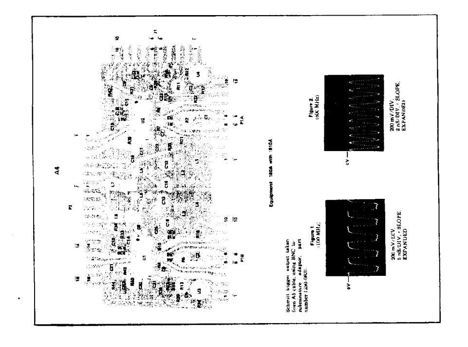
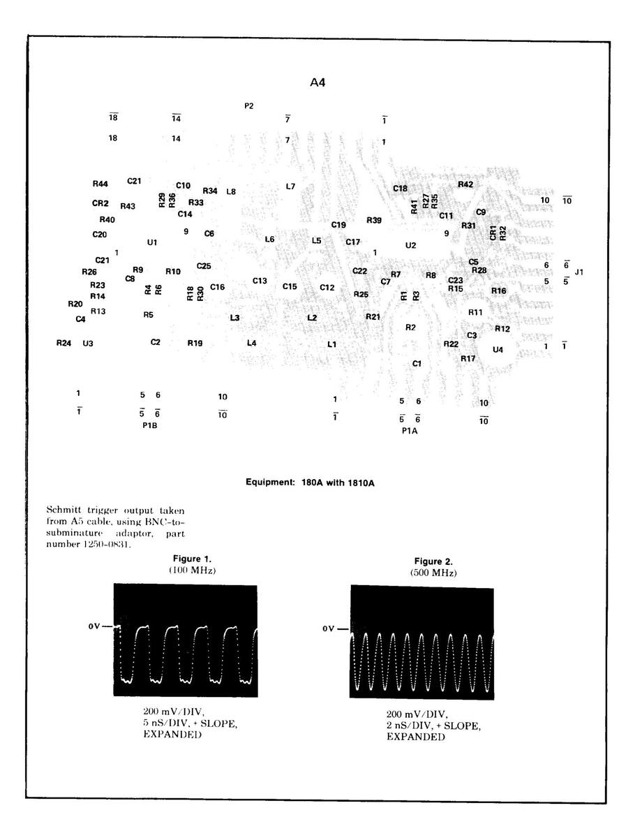
- 5. Disconnect the two white cables connected to the A9 board. Channel A output cable is the longer of the two. Connect these cables through an adapter connector (HP part number 1250–0831) to the oscilloscope's inputs.
- 6. Adjust A4R2 and A4R11 (Channel B, A4R5 and A4R13) for a signal on oscilloscope.
- Adjust A4R11 (Channel B. A4R13) for no change in signal when SLOPE switch changes position
- 8. Aiust A4R2 (Channel B. A4R45) for 50% duty cycle.
- Set 8640B output to 20 mV rms. q
- 10. Adjust A4R11 (Channel B, A4R13) for no change in signal when SLOPE switch changes position. Readjust A4R2 (Channel B, A4R5) for 50% duty cycle if required.
A4 INPUT TRIGGER
Equipment:
HP 3480A/3482A DVM
- HP 180A Oscilloscope with 1810A Sampler
- HP 8640B Signal Generator
NOTE
Allow a 5-minute warmup before performing adjustment procedure.
The following adjustments are done with the bottom cover and bottom air filter removed. The front panel display assembly is installed in the instrument. See Section III for removal of air filter.
Bias Adjustm
- Adjust A4R2 (Channel B, A4R5) offset pot to midpoint. Connect 412A to A4U2 pin 3 (Channel B, A4U1 pin 3).
- 2 Adjust A4R16 (Channel B, A4R19) bias pot for a reading of +800 mV ±50 mV.
NOTE
NOTE - If A4U2 (Channel A) or A4U1 (Channel B) are replaced, the value of A4R15 (Channel A) or A4R18 (Channel B) may have to be increased in value to meet the 800 mV ±50 mV specifications. An increase of approximately 100 increases adjustment range of A4R16 or A4R19 approximately 100 mV.
Sensitivity Adjustment:
1. Set 5345A controls as follows:
| Input Impedance |
|---|
| ATTEN (A&B) X1 |
| Input Coupling DC |
| Input Amplifier Control SEP |
| SLOPE (A&B) + |
| LEVEL Control PRESET |
Table 5-6. Adjustment Procedures (Continued)
- 2. Set 8640B Signal Generator output to 100 MHz at 100 mV rms into 50Ω.
- 3. Set 180A Oscilloscope controls as follows:
| AC/DC | DC |
|---|---|
| MAGNIFIER | X1 |
| DISPLAY 1 | INT |
4. Set 1810 Sampler controls as follows:
| DISPLAY | FILTERED |
|---|---|
| MODE | A |
| POLARITY | + UP |
| mV/DIV | 200 |
| TIME/DIV (outer knob) | 10 nSEC |
| TIME/DIV (inner knob) | 2 nSEC |
| CW SLOPE | + |
| SCAN | SWEEP |
| DIRECT/EXPANDED | EXPANDED |
| SCAN knob | almost fully cw |
- 5. Disconnect the two white cables connected to the A9 board. Channel A output cable is the longer of the two. Connect these cables through an adapter connector (HP part number 1250-0831) to the oscilloscope's inputs.
- 6. Adjust A4R2 (Channel B, A4R5) for a signal on oscilloscope
- 7. Adjust A4R11 (Channel B, A4R13) for no change in signal when SLOPE switch changes position.
- 8. Set 8640B output to 10 mV rms.
- 9. Adjust A4R2 (Channel B, A4R5) for 50% duty cycle.
- 10. Adjust A4R11 (Channel B, A4R13) for no change in signal when SLOPE switch changes position. Readjust A4R2 (Channel B, A4R5) for 50% duty cycle if required.
Table 7-5, A3/A4 Parts List
|
Reference
Designation |
HP Part
Number |
Qty | Description |
Mfr
Code |
Mfr Part Number |
|---|---|---|---|---|---|
|
A3
A3 |
05345-60039
05345-60038 |
1 |
INPUT ATTENUATOR (OPTION 012)
INPUT ATTENUATOR ASSY (SERIES 1644) |
28480
28480 |
05345-60039
05345-60038 |
|
A3C1
A3C2 |
0160-0551
0160-0551 |
2 |
CAPACITOR-FXD .01UF +100-0% 400WVDC CER
CAPACITOR-FXD .01UF +100-0% 400WVDC CER |
28480
28480 |
0160-0551
0160-0551 |
|
A3C4
A3C5 |
0160-4531 | 2 |
CAPACITOR-FXD 2.2 ±.25PF 50WVDC CER CHIP
NOT ASSIGNED |
28480 | 0160-4531 |
|
A3C6
A3C7 |
0160-4531 |
STRAY CAPACITANCE
CAPACITOR-FXD 2.2 ±.25PF 50WVDC CER CHIP |
28480 | 0160-4531 | |
|
A 3C 9
A 3C 10 |
0160-0552
0150-0072 |
2
2 |
NUT ASSIGNED
CAPACITOR-FXD 100PF +-5% 400WVDC CER CAPACITOR-FXD 200PF +-5% 1000WVDC CER |
28480
28480 |
0160-0552
0150-0072 |
|
A3C11
A3C12 A3C13 A3C14 A3C15 |
0160-0552
0150-0072 0160-3879 0160-3879 0160-3879 |
55 |
CAPACITOR-FXD 100PF +-5% 400WVDC CEP
CAPACITOR-FXD 200PF +-5% 1003WVDC CER CAPACITOR-FXD -01UF +-20% 100WVDC CER CAPACITOR-FXD -01UF +-20% 100WVDC CER CAPACITOR-FXD -01UF +-20% 100WVDC CER |
28480
28480 28480 28480 28480 28480 |
0160-0552
0150-0072 0160-3879 0160-3879 0160-3879 |
|
A 3C 16
A 3C 17 |
0160-3879 |
CAPACITOR-FXD .01UF +-20% 100WVDC CER
NGT ASSIGNED |
28480 | 0160-3879 | |
|
A3C19
A3C20 |
0160-3876
0160-3878 |
11
41 |
NOT ASSIGNED
Capacitor-fxd 47PF +-203 200WVDC CER Capacitor-fxd 1000PF +-298 100WVDC CER |
28480
28460 |
0160-3876
0160-3878 |
|
A 3C 21
A 3C 22 A 3C 23 A 3C 24 A 3C 24 A 3C 25 A 3C 26 A 3C 26 A 3C 27 |
0160-3876
0160-3878 0160-3878 0160-3878 0160-3878 0160-3878 0160-3878 0160-3879 |
CAPACITOR-FXD 47PF +-201 2000VDC CER
CAPACITOR-FXD 1000PF +-201 1000VDC CER CAPACITOR-FXD 1003PF +-201 1000VDC CER CAPACITOR-FXD 1003PF +-201 1000VDC CER CAPACITOR-FXD 1000PF +-201 1000VDC CER CAPACITOR-FXD 1000PF +-20% 1000VDC CER CAPACITOR-FXD 0.01UF +-20% 1000VDC CER |
28480
28480 28480 28480 28480 28480 28480 28480 |
0160-3876
0160-3878 0160-3878 0160-3878 0160-3878 0160-3878 0160-3878 |
|
|
A 3CR1
A 3CR2 A 3CR3 A 3CR4 A 3CR4 A 3CR5 A 3CR6 A 3CP7 A 3CP8 |
1901-0376
1901-0376 1901-0376 1901-0376 1901-0376 1901-0040 1901-0040 1901-0040 |
4
32 |
DIODE-GEN PRP 35V 504A
DIODE-GEN PRP 35V 504A DIODE-GEN PRP 35V 504A DIODE-GEN PRP 35V 504A DIODE-SWITCHING 2NS 30V 504A DIODE-SWITCHING 2NS 30V 504A DIODE-SWITCHING 2NS 30V 504A |
28480
28480 28480 28480 28480 28480 28480 28480 23480 23480 |
1901-0376
1901-0376 1901-0376 1901-0376 1901-0376 1901-0040 1901-0040 1901-0040 |
|
A3J1A
A3J1B A3J2 A3J3 |
1251-2034
1251-2034 1250-1163 1250-1163 |
8
2 |
CONNECTOR; PC EDGE; 10-CONT; DIP SOLDER
CONNECTOR; PC EDGE; 10-CONT; DIP SOLDER CONNECTOR-RF BNC FEM SGL HOLE RR CONNECTOR-RF BNC FEM SGL HOLF RR |
71785
71785 28480 28480 |
252-10-30-300
252-10-30-300 1250-1163 1250-1163 |
|
A 301
A 302 A 303 A 304 A 305 |
1855-0225
1855-0225 1854-0215 1854-0215 1854-0215 |
2
9 |
TRANSISTOR, JFET, DUAL N-CHAN D-MODE SI
TRANSISTOR, JFET, DUAL N-CHAN D-MODE SI TRANSISTOR NPN SI PD=310MW FT=300MHZ TRANSISTOP NPN SI PD=310MW FT=300MHZ TRANSISTOR NPN SI PD=310MW FT=300MHZ |
28480
29480 04713 04713 04713 |
1855-0225
1855-0225 SPS 3611 SPS 3611 SPS 3611 |
| A 306 | 1854-0215 | TRANSISTOR NPN SI PD=310MW FT=3COMHZ | 04713 | SPS 3611 | |
|
A 3R 1
A 3R 2 |
0698-8382 | 1 |
RESISTOR 25 5% .25W C TC=0+-150
NOT ASSIGNED |
28480 | 0698-8382 |
| (FOR R3) |
1 25 1-22 29
0698-8881 |
22 |
RESISTOR 49.9 12 .5W F TC=0+-100
CONNECTOR;1+CONT SKT .033 DIA RESISTOR 900K5%.25W C TC=0+-150 |
19701
00779 28480 |
#F7C1/2-70-49R9-F
1-331677-3 0698-8881 |
|
A 3R 5
A 3R 6 (FOR R6) A 3P 7 A 3R 8 |
0698-8880
0757-0072 1251-2229 0698-8881 0698-8860 |
2 |
RESISTOR 100K 5% .15W C TC=0+-150
RESISTOR 49-9 1 3 -5W F TC=0+-100 CONNFCTOR;1CONT SKT -033 DIA RESISTOR 900K 5% .25W C TC=0+-150 RESISTOR 100K 5% .15W C TC=0+-150 |
28480
19701 00779 28480 28480 |
0698-8880
MF7C1/2-TD-4989-F 1-331677-3 0698-8881 0698-8880 |
|
A 3R 9
A 3R 10 A 3R 11 A 3R 12 A 3R 13 |
2100-0597
0683-2025 2100-0597 0683-2025 0698-8381 |
2
9 2 |
RESISTOR-VAR W/SW 100K 20% CC SPST-SW
RESISTOR 2K 5% 25% FC TC=-400/+700 RESISTOP-VAR W/SW 100K 20% CC SPST-SW RESISTOR 2K 5% 25% FC TC=-400/4700 RESISTOR 2K 5% 25% FC TC=-40/4700 |
28480
01121 28480 01121 28490 |
2100-0597
C82025 2100-0597 C82025 0698-8381 |
|
A 3R 14
A 3R 15 A 3R 16 A 3R 17 A 3R 18 |
0683-5115
0698-8381 0683-5115 0683-1055 0683-1055 |
14
2 |
RESISTOR 510 51 .25W FC TC=-400/+600
RESISTOR 50 51 .15W C TC=0+-150 RESISTOR 510 51 .25W FC TC=-400/+600 RESISTOR 1M 51 .25W FC TC=-800/+900 RESISTOR 1M 51 .25W FC TC=-800/+900 |
01121
28480 01121 01121 01121 |
C85115
O698-8381 C85115 C81055 C91055 |
|
A 3P 19
A 3P 20 A 3P 21 A 3P 22 A 3P 22 A 3P 23 |
0698-8615
0698-8615 0757-0420 0698-6241 0757-0420 |
4
6 2 |
RESISTOR 75K 1% 1/20W
RESISTOR 75K 1% 1/20W RESISTOR 75K 1% 1/20W RESISTOR 750 1% +125W F TC=0+-100 RESISTOR 750 1% +125W F TC=0+-100 |
28480
28480 24546 01121 24546 |
0698-8615
0698-8615 C4-1/R-T0-751-F 877515 C4-1/8-T0-751-F |
|
A 3F 24
A 3R 25 A 3R 26 ► A 3R 27 A 3R 28 |
0757-0420
0698-6241 0757-0420 0683-1125 0698-8615 |
RESISTUR 750 13 .125W F TC=0+-100
RESISTUR 750 53 .125W CC TC=0+882 RESISTUR 750 13 .125W F TC=0+-100 RESISTOR 1.1K 53 .25W FC TC=-400/+700 RESISTOR 75K 1% 1/20W |
24546
01121 24546 01121 28480 |
C4-1/8-T0-751-F
B87515 C4-1/8-T0-751-F C81125 0698-8615 |
NOT IN OPTION 012.
See introduction to this section for ordering information
| Table | 7-5 | A3/A4 | Parts 1 | List ( | (Continued) |
|---|
|
Reference
Designation |
HP Part
Number |
Qty | Description |
Mfr
Code |
Mfr Part Number |
|---|---|---|---|---|---|
|
A 3R 29
► A 3R 30 A 3R 31 A 3R 32 A 3R 33 |
0698-8615
0698-6283 0683-1525 0698-5178 0698-5178 |
2
1 5 4 |
RESISTOR 75K 1% 1/20W
RESISTOR 10 5% -125W CC TC=0+588 RESISTOR 1.5K 5% -25W FC TC=-400/+700 RESISTOR 1.5K 5% -125W CC TC=0+882 RESISTOR 100 5% -125W CC TC=0+588 |
28480
01121 01121 01121 01121 01121 |
0698-8615
881005 C21525 881525 881525 881015 |
|
A 3R 34
A 3R 35 A 3R 36 A 3R 37 A 3R 38 |
0757-0802
0698-3113 0757-0802 0698-3378 0683-1025 |
2
17 2 |
RESISTOR 162 1% -5W F TC=0+-100
RESISTOR 100 5% -125W CC TC=0+588 RESISTOR 162 1% -5W F TC=0+-100 RESISTOR 51 5% -125W CC TC=0+588 RESISTOR 1000 5% -25W CC TC=-400/+800 |
19701
01121 19701 01121 01121 |
MF7C-1/2-T0-162R-F
BB1015 MF7C-1/2-T0-162R-F BB5105 CB1025 |
|
► A 3P 39
A 3R 40 A 3R 41 A 3R 42 A 3R 43 |
0698-3378
0683-1025 0698-3113 0698-3113 0698-6984 |
2 |
RESISTOR 51 5% .25W CC TC=-400/+800
RESISTOR 1000 5% .25W CC TC=-400/+800 RESISTOR 100 5% .125W CC TC=-400/+808 RESISTOR 100 5% .125W CC TC=0+588 RESISTOR 470 5% .125W CC TC=0+882 |
01121
01121 01121 01121 01121 01121 |
BB5105
CB1025 B81015 B81015 B81015 B84715 |
|
A 3R 44
A 3R 45 A 3R 46 A 3R 47 A 3R 48 |
21001788
06832415 0698-6984 21001788 0698-5564 |
41 |
RESISTOR-VAR TRMR 500 DHM 10% C TOP ADJ
RESISTOR 240 5% .25% FC TC=-400/+609 RESISTOR 470 5% .125% CC TC=0+882 RESISTOR-VAR TKMR 500 DHM 10% C TOP ADJ RESISTOR 240 5% .125% CC TC=0+882 |
84048
01121 01121 84048 01121 |
170-501
CB2415 BB4715 170-501 BB2415 |
|
0698-6283
0683-1125 0683-1125 0698-3378 0683-4715 |
8
18 |
RESISTOR 10 5% .125W CC TC=0+588
RESISTOR 1.1K 5% .25W FC TC=-400/+700 RESISTOR 1.1K 5% .25W FC TC=-400/+700 RESISTOR 51 5% .125W CC TC=0+588 RESISTOR 470 5% .25W FC TC=-400/+600 |
01121
01121 01121 01121 01121 01121 |
881005
C81125 C81125 BR5105 CR4715 |
|
A 38.57
A 38.59 A 38.59 to A 38.62 A 35 1 (FOR S1) A 35 2 (FOR S2) A 35 3 (FOR S3) |
0698-3378
0683-4715 0683-5105 05345-60100 1460-0603 05345-60100 1450-0603 05345-60101 5022-3440 |
6
6 1 1 |
RESISTOR 51 51 .125W CC TC=0+588
RESISTOR 470 51 .25W FC TC=-400/+600 RESISTOR 51 OHM 5% WW CF LEVER/SLIDE ASSY SPRING WFRM .014-0D MUW LEVER/SLIDE ASSY SPRING WFRM .014-0D MUW SLIDE ASSY, P.C. SWITCH SPRING, DETENT |
01121
01121 01121 28480 28480 28480 28480 28480 28480 |
885105
C84715 C85105 05345=60100 1460-0603 05345-60100 1460-0603 C5345-60100 15070-3440 |
|
A 354
(FOR S4) A 355 (FOR S5) A 356 (FOR S6) |
05345-60100
1460-0603 05345-60100 1460-0603 05345-60100 1460-0603 |
LEVER/SLIDE ASSY
SPRING WEPM .014-OD MUW LEVER/SLIDE ASSY SPRING WERM .014-OD MUW LEVER/SLIDE ASSY SPRING WERM .014-OD MUW |
28480
26480 28480 28480 28480 26480 28480 |
UD34D-60100
1460-0603 05345-60100 1460-0603 05345-60100 1460-0603 |
|
|
A 35 7
(FOR 57) A 35 8 A 35 5 |
05345-60100
1460-0603 3101-1596 3101-1596 |
2 |
LEVER/SLIDE ASSY
Spring WERM .014-DD MUW Switch-Sl dpdt-ns Mintr 1A 125VAC Switch-Sl dpdt-ns Mintr 1A 125VAC |
28480
28480 28480 28480 28480 |
05345-60100
1460-0603 3101-1596 3101-1596 |
|
A 3U 1
A 3U 2 |
1 826~0088
1826-0088 |
Z |
IC, LIN 114-BIT WINE BAND AMPL
IC, LIN 114-BIT WIDE BAND AMPL |
28480
28480 |
1826-0088
1826-0088 |
| 05345-40002 | 4 | GUIDE (SWITCH TRACK) | 28480 | 05345-40002 | |
| A4 | 05345-60004 | 1 | INPUT TRIGGER ASSY (SERIES 1612) | 28480 | 05345-60004 |
|
A4C1
A4C2 A4C3 A4C4 A4C5 |
0160-3879
0160-3879 0160-3879 0160-3879 0160-3879 0160-3878 |
CAPACITOR-FXD .01UF +-20% 100WVDC CER
CAPACITOP-FXD .01UF +-20% 100WVDC CER CAPACITOR-FXD .01UF +-20% 100WVDC CER CAPACITOR-FXD .01UF +-20% 100WVDC CER CAPACITOR-FXD 1000PF +-20% 100WVDC CER |
28480
28480 28480 28480 28480 28480 |
0160-3879
0160-3879 0160-3879 0160-3879 0160-3878 |
|
|
A4C6
A4C7 A4C8 A4C9 A4C10 |
0160-3878
0160-3878 0160-3878 0160-3878 0160-3878 |
CAPACITOR-FXD 1000 PF +-20% 100WVDC CER
CAPACITOR-FXD 1000 PF +-20% 100WVDC CER CAPACITOR-FXD 1000 PF +-20% 100WVDC CER CAPACITOR-FXD 1000 PF +-20% 100WVDC CER CAPACITOR-FXD 1000 PF +-20% 100WVDC CER |
28480
28480 28480 28480 28480 28480 |
0160-3878
0160-3878 0160-3878 0160-3878 0160-3878 0160-3878 |
|
|
A4C 11
A4C 12 A4C 13 A4C 14 A4C 15 |
0160-3876
0180-0428 0180-0429 0160-3876 0180-0428 |
4 |
CAPACITOR-FXD 47PF +-20% 200WVOC CER
CAPACITOR-FXD; 68UF+-20% 6VDC TA-SOLID CAPACITOR-FXD; 68UF+-20% 6VDC TA-SOLID CAPACITOR-FXD 47PF +-20% 6VDC TA-SOLID CAPACITOR-FXD; 68UF+-20% 6VDC TA-SOLID |
28480
28480 28480 28480 28480 28480 |
0160-3876
0180-0428 0180-0428 0160-3876 0180-0428 |
|
A4C16
A4C17 A4C18 A4C19 A4C20 |
0 180-0428
0160-3876 0160-3878 0160-3879 0160-3879 0160-3876 |
CAPACITOR-FXD; 68UF+-20% 6VDC TA-SOLID
CAPACITOR-FXD 47PF +-20% 200WVDC CER CAPACITOR-FXD 1000PF +-20% 100WVDC CER CAPACITOR-FXD +01UF +-20% 100WVDC CER CAPACITOR-FXD 47PF +-20% 200WVDC CER |
28480
28480 28480 28480 28480 28480 |
0180-0428
0160-3876 0160-3878 0160-3879 0160-3876 |
|
|
A4C21
A4C22 A4C23 A4C24 A4C25 A4CR1 A4CR1 |
0160-3879
0160-3876 0160-3876 0160-3876 0160-3876 1902-0074 |
3 |
CAPACITOR-FXD 1000PF +-20% 100WVDC CER
CAPACITOR-FXD 47PF +-20% 200WVDC CER CAPACITOR-FXD 47PF +-20% 200WVDC CER CAPACITOR-FXD 47PF +-20% 200WVDC CER CAPACITOR-FXD 47PF +-20% 200WVDC CER DIODE-ZNR 7.15V 5% DO-7 PD=.4W TC=+.047% DIODE-ZNR 7.15V 5% DO-7 PD=.4W TC=+.047% |
28480
28480 28480 28490 28490 28480 04713 04713 |
0160-3878
0160-3876 0160-3876 0160-3876 0160-3876 0160-3876 SZ 10939-140 SZ 10939-140 |
NOT IN OPTION 01
See introduction to this section for ordering information
Table 7-5. A3/A4 Parts List (Continued)
| · | |||||
|---|---|---|---|---|---|
|
Reference
Designation |
HP Part
Number |
Qty | Description |
Mfr
Code |
Mfr Part Number |
|
A4CR3
A4CR4 |
1902-3036 | DIODE ZENER 3.16V 5% DO-7.4W | 04713 | SZ 10939-38 | |
| A4L1 | 9100-1788 | 5 | COLL: FXD: NON-MOLOED RE CHOKE: .750H | 04/13 | SZ 10939-38 |
| A4L2 | 9100-1788 | COIL: FXD; NON-MOLDED RF CHOKE: .750H | 02114 | VK200-20/48 | |
| A4L3 | 9100-1788 | COIL: FXD: NON-MOLDED RF CHOKE: .750H | 02114 | VK200-20/48 | |
| A4L5 | 9100-1620 | 2 |
COIL; FXD; NON-MOLDED RF CHOKE; .75UH
COIL-FXD MOLDED RF CHOKE 15UH 10% |
02114
24226 |
VK200-20/48
15/152 |
| A4L 6 | 9100-1620 | COIL-FXD MOLDED RE CHOKE 150H 10% | 76.226 | 15/152 | |
|
44L 7
84L 8 |
9100-0549
9100-0549 |
2 |
COIL-FXD MOLCED RF CHOKE 220H 10%
COIL-FXD MOLDED RF CHOKE 220H 10% |
06560
06560 |
4422-8K
4422-8K |
| A4R1 | 0698-5178 | RESISTOR 1.5K 5% .125W CC TC=0+882 | 01 1 2 1 | BB1525 | |
| A4R3 | 0698-5178 | RESISTOR-VAR TRMR 500 DHM 10% C TOP ADJ | 84048 | 170-501 | |
|
448 4
448 5 |
0698-5178
2100-1789 |
· |
RESISTOR 1.5K 5% .125W CC TC=0+882
RESISTOR-VAR TRMR 500 OHM 10% C TOP ADJ |
01121
84048 |
881525
881525 170-501 |
| A4R6 | 0698-5178 | RESISTOR 1.5K 5% .125W CC TC=0+882 | 01121 | RR1525 | |
| A4P 7 | 0698-3378 | RESISTOR 51 5% +125W CC TC=0+588 | 01121 | B85105 | |
| A4R9 | 0698-3378 | ĺ | RESISTOR 51 5% .125W CC TC=0+588 | 01121 | 885105 |
| A4R10 | 0698-3378 |
RESISTOR 51 5% +125W CC TC=0+588
RESISTOR 51 5% +125W CC TC=0+588 |
01121
01121 |
885105
885105 |
|
|
A 4R 11
A 4F 17 |
2100-3216 | 2 | RESISTOR-VAR TRMR 10KOHM 20% C TOP ADJ | 32997 | 3339H-1-103 |
| A 4P 13 | 2100-3216 | 2 | RESISTOR-VAR TRMP TOKOUN 200 C TOO ACT | 28480 | 0698-8623 |
|
A4R 14
A4R 15 |
0698-8623
0757-0913 |
з | RESISTOR 360 2% .125W F TC=0+-100 |
32997
28480 24546 |
5559H-1-103
0698-8623 C4-1/8-T0-361-G |
| A48 16 | 2100-1984 | 2 | RESISTOR-VAR TRMR 100 OHM 102 C TOP ADI | 84049 | 170=1.01 |
| A4R17 | 0698-5183 | 2 | RFSISTOR 4.3K 5% .125W CC TC=0+882 | 01121 | 884325 |
| A4R19 | 0/5/-0913 | RESISTOR 360 2% .125W F TC=0+-100 | 24546 | C4-1/8-TO-361-G | |
| 44R 20 | 0698-5183 |
RESISION-VAR TRMK 100 OHM 10% C TOP ADJ
RESISTOR 4.3K 5% .125W CC TC=0+882 |
84048
01121 |
170-101
BB4325 |
|
|
A 4 P 21
A 4 R 22 |
0686-6815 | 2 | RESISTOR 680 52 .5W CC TC=0+529 | 01121 | E86815 |
| 44R 23 | 0686-6815 | · ' | RESISTOR 680 5% -5% CC TC=0+529 | 24546 | C4-1/8-T0-201-F |
|
A4R 24
A4R 25 |
0757-0407
0683-1125 |
RESISTOR 200 1% .125W F TC=0+-100
RESISTOR 1.1K 5% - 25W FC TC=-600/+700 |
24546 | C4-1/8-T0-201-F | |
| A48.26 | 0693-1125 | 01121 | |||
| A46.27* | 0683-5105 | 9 | RESISTOR 51 51 52 +25W FC TC=+400/+700 |
01121
01121 |
C81125
C85105 |
| A4F 28 | 2683-1125 |
PESISTORY SELECTED PART
RESISTOR 1.1K 5% .25W FC TC=-400/+700 |
01121 | CB1125 | |
| A4R 29* | 0683-5105 |
RESISTOR 51 5% .25W FC TC=-400/+500
*FACTORY SELFCTED PART |
01121 | CB5105 | |
| A4F 30 | 0683-1125 | RESISTOR 1.1K 58 .25H FC TC=-400/+700 | 01121 | C81125 | |
| A 4R 32 | 0683-4715 |
RESISTOR 51 58 .125W CC TC=0+588
RESISTOR 470 58 .25W EC TC==400/4400 |
01121 | 885105 | |
| A 4P 33 | 0698-3378 | RESISTOR 51 5% .125W CC TC=0+583 | 01121 |
CB4715
BB5105 |
|
| A 4R 34 | 0683-4715 | RESISTOR 470 5% +25W FC TC=+400/+600 | 01121 | C84715 | |
|
A4R 35
A46 36 |
0683=2425 | 4 | RESISTOR 2.4K 5% .25W FC TC=-400/+700 | 01121 | CB2425 |
| A4P 39 | 0698-3111 | 2 | RESISTOR 30 5% +125W CC TC=0++850 | 01121 | |
|
48 40
449 41 |
0698-3111 | _ | RESISTOR 30 5% .125W CC TC=0+-850 | 01121 | BB3005 |
| #4R 42 | 0683-1615 | 2 | RESISTOR 160 52 -254 EC TC==400/4600 | 01121 | 682102 |
|
A 4R 43
A 4P 44 |
0698-3378
0683-1615 |
RESISTOR 51 57 .125W CC TC=0+588
RESISTOR 160 57 .25W FC TC=-400/4400 |
01121 |
885105
681415 |
|
| A401 | 1826-0290 | |,| | IC:AMPLIFIER | 20400 | |
| A4U2 | 1826-0290 | - L | IC:AMPLIFIER | 28480 | 1826-0290 |
|
A4U3
A4U4 |
1826-0021
1826-0021 |
2 |
IC:LM310H
IC:LM310H |
27014
27014 |
LM310H
LM310H |
See introduction to this section for ordering information
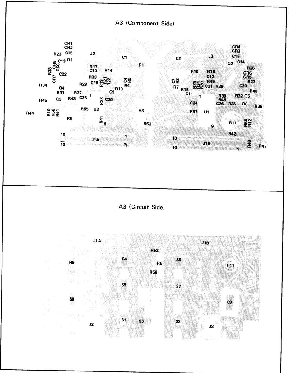
Figure 7-3. A3 Input Attenuator Assembly
VII

Operating and Service Manual
HP 5345A Electronic Counter
HP 5345A ELECTRONIC COUNTER
OPERATING AND SERVICE MANUAL
HP 5345A SERIAL PREFIX: 3103
This manual applies directly to HP 5345A Electronic Counters having serial number prefix 3103.
NEWER INSTRUMENTS
This manual, with enclosed "Manual Changes" sheet, applies to HP 5345A Electronic Counters having serial number prefixes as listed on the "Manual Changes" sheets.
OLDER INSTRUMENTS
For serial prefixes below 3103, refer to Section VII for manual backdating.
©HEWLETT-PACKARD COMPANY 1986, 1994 5301 STEVENS CREEK BLVD, SANTA CLARA, CA 95052-8059

MANUAL PART NUMBER : 05345-90060
Printed: MAY 1994

CERTIFICATION
Hewlett-Packard Company certifies that this product met its published specifications at the time of shipment from the factory. Hewlett-Packard further certifies that its calibration measurements are traceable to the United States National Bureau of Standards, to the extent allowed by the Bureau's calibration facility, and to the calibration facilities of other International Standards Organization members.
WARRANTY
This Hewlett-Packard instrument product is warranted against defects in material and workmanship for a period of one year from date of shipment. During the warranty period, Hewlett-Packard Company will, at its option, either repair or replace products which prove to be defective.
For warranty service or repair, this product must be returned to a service facility designated by HP. Buyer shall prepay shipping charges to HP and HP shall pay shipping charges to return the product to Buyer. However, Buyer shall pay all shipping charges, duties, and taxes for products returned to HP from another country.
HP warrants that its software and firmware designated by HP for use with an instrument will execute its programming instructions when properly installed on that instrument. HP does not warrant that the operation of the instrument, or software, or firmware will be uninterrupted or error free.
LIMITATION OF WARRANTY
The foregoing warranty shall not apply to defects resulting from improper or inadequate maintenance by Buyer, Buyer-supplied software or interfacing, unauthorized modification or misuse, operation outside of the environmental specifications for the product, or improper site preparation or maintenance.
NO OTHER WARRANTY IS EXPRESSED OR IMPLIED. HP SPECIFICALLY DISCLAIMS THE IMPLIED WARRANTIES OF MERCHANTABILITY AND FITNESS FOR A PARTICULAR PURPOSE.
EXCLUSIVE REMEDIES
THE REMEDIES PROVIDED HEREIN ARE BUYER'S SOLE AND EXCLUSIVE REMEDIES. HP SHALL NOT BE LIABLE FOR ANY DIRECT, INDIRECT, SPECIAL, INCIDENTAL, OR CONSEQUENTIAL DAMAGES, WHETHER BASED ON CONTRACT, TORT, OR ANY OTHER LEGAL THEORY.
ASSISTANCE
Product maintenance agreements and other customer assistance agreements are available for Hewlett-Packard products.
For any assistance, contact your nearest Hewlett-Packard Sales and Service Office. Addresses are provided at the back of this manual.
TABLE OF CONTENTS
| Section | Title | Page |
|---|---|---|
| I. GE | NERAL INFORMATION | 1-1 |
| - 1-1 | . Description | 1-1 |
| 1-4 | . Instrument Identification and Manual Changes | 1-1 |
| 1-6 | Options | 1-1 |
| 1-8 | . Accessories | 1-1 |
| II. IN | STALLATION | 2-1 |
| 2-1 | . Introduction | 2-1 |
| 2-3 | Unpacking and Inspection | 2-1 |
| 2-5 | Power Requirements | 2-1 |
| 2-7 | Line Voltage Selection | 2-1 |
| 2-1 | 3. Power Cable | 2-2 |
| 2-1 | 5. HP-IB Interface Connections | 2-3 |
| 2-1 | 9. HP-IB Talk/Listen and Address Switches | 2-4 |
| 2-2 | 2. HP-IB Descriptions | 2-4 |
| 2-2 | 4. Repacking for Shipment | 2-4 |
| 2-2 | 6. Environment During Storage and Shipment | 2-4 |
| III. OF | PERATION AND PROGRAMMING | 3-1 |
| 3-1 | . Introduction | 3-1 |
| 3-3 | . Measurement Technique | 3-1 |
| 3-5 | Operating Modes | 3-1 |
| 3-7 | 7. Frequency Mode | 3-1 |
| 3-1 | 0. Period Modes | 3-1 |
| 3-1 | 5. Time Interval Modes | 3-2 |
| 3-2 | 4. Ratio Measurements | 3-3 |
| 3-2 | 9. Totalize Mode | 3-4 |
| 3-3 | 4. Input Triggering | 3-4 |
| 3-3 | 6. Excessive Gate Time | |
| 3-3 | 8. External Arming and Gating | 3-5 |
| 3-4 | 0. External Arming | 3-5 |
| 3-4 | 2. External Gating | 3-6 |
| 3-4 | 7. Time Interval Measurements | 3-6 |
| 3-5 | 1. Display | 3-8 |
| 3-5 | 3. Display Position | 3-8 |
| 3-5 | 5. Asterisk | 3-8 |
| 3-5 | 9. Arm Light | 3-8 |
| . 3-6 | 61. Gate Light | 3-8 |
| 3-6 | 3. Lamp Test | 3-8 |
| 3-6 | 6. Cooling | 3-9 |
| 3-6 | Air Filter Cleaning | 3-9 |
| 3-7 | 70. Remote Programming via the Hewlett-Packard Interface Bus | 3-25 |
| 3-7 | 1. Introduction | 3-25 |
| 3-7 | 74. Interface System Terms | 3-25 |
| 3-7 | 6. HP-IB Description | 3-26 |
| 3-8 | 4. HP-IB Control Lines | 3-26 |
| 3-8 | 35. HP-IB Transfer Control Lines | 3-27 |
| 3-8 | 38. Address Selection | 3-27 |
| 3-9 | 01. Addressing the 5345A for Talk and Listen | 3-28 |
| 3-9 | 03. Output Modes | 3-28 |
| 3-9 | 95. Computer Dump | 3-28 |
| 3-9 | 99. Talk Output Mode | 3-29 |
| 3-1 | 01. Programming Commands | 3-29 |
| 3-1 | .04. Program Function Descriptions | 3-29 |
HP 5345A Table of Contents
TABLE OF CONTENTS (Continued)
| Section | Title | Page |
|---|---|---|
| 3-10 | 5. Program Codes and Universal Commands for Option 012 | |
| 3-107 | 7. Modes of Operation | 3-34 |
| 3-110 | ). Starting a Measurement Procedure | 3-35 |
| 3-112 | 2. Programming Examples | 3-35 |
| 3-115 | 5. Example Program 1: Triggering a Measurement | 3-35 |
| 3-117 | 7. Example Program 2: Start/Stop Totalize | 3-36 |
| 3-119 |
|
3-37 |
| 3-121 | Example Program 4: Computer Dump Mode | 3-38 |
| 3-123 | 8. Option 012 Factory Installed Remote Programming | 3-39 |
| 3-126 | 5. Features | 3-39 |
| 3-128 |
|
3-40 |
| 3-130 | ). Example Program: Time Interval Measurements of Pulse Width | 3-40 |
| IV. THE | ORY OF OPERATION | 4-1 |
| 4-1. | Introduction | |
| 4-3 | Logic Elements | 4-1 |
| 4-5. | Logic Levels | |
| 4-7 | Wire-OR/Wire-AND Configuration | 4-2 |
| 4-10 | 4-2 | |
|
4_10.
4_12 |
Integrated Circuits — Theory of Operation |
4-2
4_2 |
|
-12.
A_14 |
Synchronous 4-Bit Un/Down Counter 1820-0233 | 4-3 |
| 4-14. | Read-Only Memory (ROM) 1820-0200-0200 | |
| 4 19 | A Bit Bistable Lateb 1890.0301 | |
| 4-10. | 4-Dit Distable Later, 1020-0501 | |
| 4-20. | Duel Four Input Multiplever 1820-0610 | |
|
4-22.
1.91 |
One of Tan Decoder 1820-0627 | |
| 4-24. | MOS Sir Decede Counter, 1820-0624 | |
| 4-20. | Fight Input Multiplever 1820-0658 | |
|
4-20.
4 20 |
Cued Leteh 1820 0701 | |
| 4-00. | Quad Later, 1020-0701 | |
| 4-32. | One-of-Sixteen Decoder, 1020-0702 | |
| 4-04. | Quad Two-Input Multiplexer, 1820-0716 | |
| 4-30. | Synchronous 4-Dit Counter, 1820-0710 | |
| 4-00. | 5 Bit Compositor 1990 0004 |
4-1
1 0 |
| 4-40. | D-Dit Comparator, 1620-0904 | |
| 4-42. | 04-Bit Read/ while Melliory, 1020-1020 | |
| 4-44. | ||
| 4-40. | ||
| 4-40. | Gale | |
| 4-01. | Scalers | |
| 4-00. | Anulineur Floresson | |
| 4-01. | State Control Section | |
| 4-00. | Oscillator Officials | |
| 4-09 | Circuit Boord Theory | |
| 4-11. | Al and A2 Dimlay Accomplica | |
| 4-13. | A1 and A2 Display Assembles | |
| 4-04. | As input Attenuator | |
|
4-90.
4 00 |
A4 IIIput Ingger |
4-13
4 19 |
|
4-93.
4 05 |
AU FIORI Faller Interconnect | |
| 4-95. | AU DWILCIMING REGULATOR | |
| 4-105 | A DII Multiplice Noice Concenter | |
| 4-110 | AO Main Cata | |
| 4-132 | A 10 Cate Control | |
| 4-140 | ||
| 4-101 | A11 DCalci | |
| 4-170 | 4-40 |
TABLE OF CONTENTS (Continued)
| Section | Title | Page | |
|---|---|---|---|
| 4-196. | A13 Register, Adder/Subtracter | 4-32 | |
| 4-219. | A14 Qualifier | 4-37 | |
| 4-241. | A15 ROM | 4-40 | |
| 4-271. | A16 Motherboard | 4-46 | |
| 4-273. | A17 Plug-In Interconnection | 4-46 | |
| 4-275. | A18 10 MHz Oscillator (Oven) | 4-46 | |
| v. | MAINTE | ENANCE AND SERVICE | 5-1 |
| 5-1. | Introduction | 5-1 | |
| 5-3. | Assembly Designations | 5-1 | |
| 5-5. | Test Equipment | 5-2 | |
| 5-7. | Adjustments and In-Cabinet Performance Check | 5-2 | |
| 5-9. | Periodic Maintenance | 5-2 | |
| 5-11. | Overall Troubleshooting | 5-2 | |
| 5-13. | Trouble Isolation Method | 5-3 | |
| 5-17. | Troubleshooting Aids | 5-3 | |
| 5-21. | Extender Board Kit (10595A) | 5-3 | |
| 5-25. | 5345A Operational Verification | 5-23 | |
| VI. | REPLAC | CEABLE PARTS | 6-1 |
| 6-1. | Introduction | 6-1 | |
| 6-3. | Reference Designations | 6-1 | |
| 6-5. | Replaceable Parts | 6-1 | |
| 6-8. | How to Order a Part | 6-1 | |
| 6-10. | Parts Identification | 6-1 | |
| 6-14. | Contacting Hewlett-Packard | 6-2 | |
| 6-18. | Cabinet Parts and Hardware | 6-2 | |
| VII. | . OPTION | IS AND MANUAL CHANGES | 7-1 |
| 7-1. | Introduction | 7-1 | |
| 7-3. | Options | 7-1 | |
| 7-5. | Field Installation of Options | 7-1 | |
| 7-8. | Manual Changes | 7-1 | |
| 7-10. | Newer Instruments | 7-1 | |
| 7-12. | Older Instruments | 7-1 | |
| VII | I. SCHE | MATIC DIAGRAMS | 8-1 |
| 8.1 | Schematic Diagrams | 8-1 | |
| 8-3. | Schematic Diagram Notes, Assembly Numbers, and Reference Designations | 8-1 | |
| 8-5. | Reference Designations | 8-1 | |
| 8-7. | Identification Markings on Printed-Circuit Boards | 8-1 |
SAFETY CONSIDERATIONS
GENERAL
This is a Safety Class I instrument. This instrument has been designed and tested according to IEC Publication 348, "Safety Requirements for electronic Measuring Apparatus", and has been supplied in safe condition.
OPERATION
BEFORE APPLYING POWER verify that the power transformer primary is matched to the available line voltage and the correct fuse is installed (see Section II, Paragraph 2-6.) Make sure that only fuses with the required rated current and of the specified type (normal blow, time delay, etc.) are used for replacement. The use of repaired fuses and the short-circuiting of fuseholders must be avoided.
SERVICE
Although this instrument has been designed in accordance with international safety standards, this manual contains information, cautions, and warnings which must be followed to ensure safe operation and to retain the instrument in safe condition. Service and adjustments should be performed only be qualified service personnel.
Any adjustment, maintenance, and repair of the opened instrument under voltage should be avoided as much as possible, and when inevitable, should be carried out only by a skilled person who is aware of the hazard involved.
Capacitors inside the instrument may be charged even if the instrument has been disconnected from its source of supply.
Whenever it is likely that the protection has been impaired, the instrument must be made inoperative and be secured against any unintended operation.
ACCOUSTIC NOISE EMISSION:
LpA 56 dB at operator position, at normal operation, tested per EN27779. All data are the results from type test
GERAeUSCHEMISSION:
LpA 56 dB am Arbeitsplatz, normaler Betrieb, Geprueft nach EN277779 Teil 19. Die Angaben beruhen auf Ergenbnissen von Typpruefungen.
WARNING
IF THIS INSTRUMENT IS TO BE ENERGIZED VIA AN AUTO-TRANSFORMER (FOR VOLTAGE REDUCTION) MAKE SURE THE COMMON TERMINAL IS CONNECTED TO THE EARTHED POLE OF THE POWER SOURCE.
WARNING
BEFORE SWITCHING ON THE INSTRUMENT, THE PRO-TECTIVE EARTH TERMINALS OF THE INSTRUMENT MUST BE CONNECTED TO THE PROTECTIVE CONDUCTOR OF THE (MAINS) POWER CORD. THE MAINS PLUG SHALL ONLY BE INSERTED IN A SOCKET OUTLET PROVIDED WITH A PRO-TECTIVE EARTH CONTACT. THE PROTECTIVE ACTION MUST NOT BE NEGATED BY THE USE OF AN EXTENSION CORD (POWER CABLE) WITHOUT A PROTECTIVE CONDUCTOR (GROUNDING).
WARNING
THE SERVICE INFORMATION FOUND IN THIS MANUAL IS OFTEN USED WITH POWER SUPPLIED AND PROTECTIVE COVERS REMOVED FROM THE INSTRUMENT. ENERGY AVAIL-ABLE AT MANY POINTS MAY, IF CONTACTED, RESULT IN PERSONAL INJURY.
CAUTION
BEFORE SWITCHING ON THIS INSTRUMENT:
- 1. MAKE SURE THE INSTRUMENT IS SET TO THE VOLT-AGE OF THE POWER SOURCE.
- 2. ENSURE THAT ALL DEVICES CONNECTED TO THIS INSTRUMENT ARE CONNECTED TO THE PRO-TECTIVE (EARTH) GROUND.
- 3. ENSURE THAT THE LINE POWER (MAINS) PLUG IS CONNECTED TO A THREE-CONDUCTOR LINE POWER OUTLET THAT HAS A PROTECTIVE (EARTH) GROUND. (GROUNDING ONE CONDUCTOR OF A TWO-CONDUCTOR OUTLET IS NOT SUFFICIENT.)
- 4. MAKE SURE THAT ONLY FUSES WITH THE REQUIRED RATED CURRENT AND OF THE SPECIFIED TYPE (NORMAL BLOW, TIME DELAY, ETC.) ARE USED FOR REPLACEMENT. THE USE OF REPAIRED FUSES AND THE SHORT-CIRCUITING OF FUSE HOLDERS MUST BE AVOIDED.
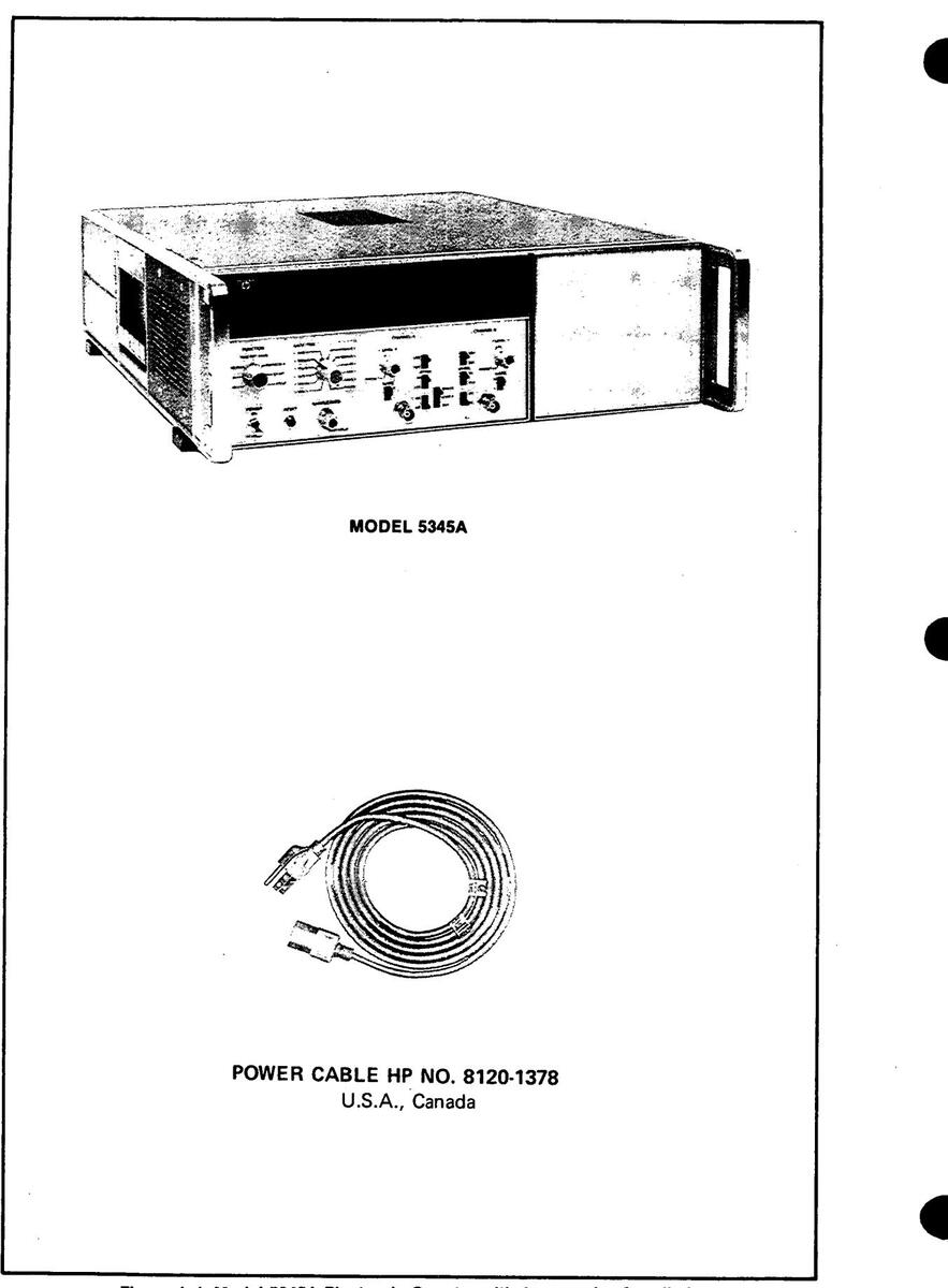
Figure 1-1. Model 5345A Electronic Counter with Accessories Supplied

SECTION I GENERAL INFORMATION
1-1. DESCRIPTION
1-2. The Hewlett-Packard Model 5345A Electronic Counter is a reciprocal counter capable of direct measurements to 500 MHz. The counter's ability to accept plug-in accessories extends its inherent capabilities and provides for a variety of additional measurements.
1-3. The instrument measures frequency, period, period average, single-shot time interval, time interval average, and ratio. It also provides a totalize function, whereby two signals can be simultaneously totalized with the displayed result being the sum of difference in the total number of counts.
1-4. INSTRUMENT IDENTIFICATION AND MANUAL CHANGES
1-5. Hewlett-Packard instruments have a 2-section, 10-character serial number (0000A00000), which is located on the rear panel. The 4-digit serial prefix identifies instrument changes. If the serial prefix of your instrument differs from that listed on the title page of this manual, there are differences between this manual and your instrument. instruments having lower serial prefixes than that listed on the title page are documented in Section VII, and higher serial prefixes are covered with manual change sheets included with the manual. If the manual change sheet is missing, contact the nearest Hewlett-Packard Sales office listed at the back of this manual.
1-6. OPTIONS
1-7. The following is a list of options: Option 011, General Purpose I/O (provides digital output and input control over all functions, except input amplifier); Option 012, similar to Option 011, but includes slope and level control. Option 908, Rack Mounting Kit, is available at an additional cost when ordered at the same time as the instrument.
1-8. ACCESSORIES
1-9. Table 1-1 lists equipment supplied and Table 1-2 list accessories available.
| Table 1-1. Equipment Supplie |
|---|
| DESCRIPTION | HP PART NO. |
|---|---|
| Detachable Power Cord, 231 cm (7½ ft. long) | 8120-1378 |
Table 1-2. Accessories Available
| DESCRIPTION | HP PART NO. |
|---|---|
| Rack Mounting Kit | 5060-8740 |
| Board Extender Kit | 10595A |
| Plug-In Adapter | 10590A |
| 10 MΩ Probe Kit | 10004D |
| 50Ω Probe Kit | 10020A |

1 ATTEXT

Input Characteristics Channel A and Channel R
SEPARATE INPUTS
Dange:
DC coupled: 0 to 500 MHz AC coupled: 1 MΩ. 200 Hz to 500 MHz 50Ω, 4 μ Hz to 500 MHz
Impedance : Switch selectable. 1 MQ (nominal) shunted by approximately 45 pF or 50Ω (nominal).
Sensitivity: (preset) 500 and 1 MO
50Ω DC coupled 0 to 300 MHz, 25 mV rms 300 MHz to 500 MHz, 50 mV rms The to 300 MHz, 25 mVrms 500 A AC couple
300 MHz to 500 MHz 50 mV rms X1: 25 mV rms sine wave 75 mV p-p pulse
X10: 300 mV rms sine wave, 900 mV p-p pulse
Dynamic Range: (preset) 50Ω and 1 MΩ X1: 25 mV to 300 mV rms sine wave 75 mV to 900 mV p-p pulse X10: 300 mV to 2.0V rms sine wave 900 mV to 6.0V p-p pulse
Linear Operating Range: -2.0 to +2.0V dc (nominal)
| Preset: | Centers trigger level to 0V dc (nominal) at 25°C |
|---|---|
| Drift: | ±10 mV dc max., 0°C to 50°C |
| Output: | Channel A & B trigger voltages (X ATTEN) |
| - | available t rear panel BNC connectors. |
| Accuracy: | X1: ±15 mV |
| - | X10: ±150mV (nominal) |
Slope: Independent selection of positive or negative slope.
Maximum Input: Damage may occur beyond specified level. For larger inputs, voltage divider probes 10020A for 50Ω and 10004D for 10MO are recommended
| 50Ω X1: | ±7V dc |
|---|---|
| 7V rms below 5 MHz | |
| 3.5V rms (+24 dBm) 5 MHz and above | |
| X10: | 7V dc, 7V rms (+30 dBm) |
| 1MΩ X1: | ±350V dc |
| 250V rms to 20 kHz, decreasing to 3.5V rms | |
| above 5 MHz | |
| X10: | ±350V dc |
| 250V rms to 20 kHz, decreasing to 35V rms | |
| above 5 MHz |
Cross Talk: No effects if inputs to Channel A and B are both above or below 100 MHz. With one signal above 100 MHz and the other below, there are no effects if the lower frequency has a slew rate of ≥10Vµs.
COMMON INPUT
In this mode the signal is applied to Channel A through a power splitter which equalizes impedances and delays to the input amplifiers. Channel B input is disabled. Both input impedance switches should be in the same position. All specifications are the same as for separate operation with the following differences.
Range
DC coupled: 0 to 400 MHz AC coupled: 1 MQ 300 Hz to 400 MHz AC coupled: 50Ω. 4 MHz to 400 MHz
Impedance: 1 MΩ becomes 500 kΩ shunted by approximately 80 pF. 50Ω no change.
Sensitivity (preset)
50Ω X1: 50 mV rms sine wave, 150mV p-p pulse
- X10. 600 mV rms sine wave, 1.8V p-p pulse
- 1MO DC coupled: 0 to 50 MHz 25 mVrms 50 MHz to 200 MHz. 75 mVrms 200 MHz to 400 MHz 120 mV rms AC coupled: 300 Hz to 50 MHz, 25 mV rms 50 MHz to 200 MHz 75 mV rms 200 MHz to 400 MHz, 120 mV rms
Dynamic Range
- 50Ω X1: 50 mV to 600 mV rms sine wave
-
500 X1 · 150 mV to 1.8V p-p pulse
- X10: 600 mV to 4.0V rms sine wave
- X10: 1.8V to 12V p-p pulse 1 MΩ Same as in SEPARATE
Maximum Input:
- 500: +5 0V dc or 5V ms
- 1 MΩ Same as in SEPARATE
Trigger Level: Adjustable over the range +4 0V dc (X ATTEN) in 50Ω or ±2.0V dc in MΩ (XATTEN).
Trigger Level Output: Channel A and B trigger voltages times 2 (X ATTEN) available at rear panel BNC connectors.
Ассигасу:
50Ω X1: ±30 mV (nominal) X10: +300 mV (nominal) 1 MΩ: Same as in SEPARATE
Frequency/Frequency Average. Period/Period Average
Both frequency and period are measured by measuring the total elapsed time, T, for the integral number of cycles, N of the input waveform. Computation, involving the quantities of N and T. provides direct readout of either frequency or period.
Range: 50µHz to 500 mHz; 2 ns to 20,000 s.
Measurement Time: Consists of GATE TIME plus the time required to reach the next STOP trigger level. When in MIN the GATE TIME is 50 ns or one period of the input signal, whichever is greater. when the GATE TIME is set to one of the decade steps, the counter will reset if a stop trigger is not reached within 3.5 times the GATE TIME setting. Decade GATE TIME settings range from 100 ns to 1000 s.


When using EXT GATE, the measurement cycle time consists of the GATE TIME divided by the duty cycle of the EXT GATE signal plus the time required to reach the next STOP trigger level after the end of the EXT GATE pulse.
Accuracy: Resolution is nine digits per second of measurement time. With the DISPLAY POSITION switch is AUTO the least significant digit error is ±1 count if the most significant digit is 1 through 4, and ±2 counts if the most significant digit is 5 through 9.
Accuracy is ± least significant digit (LSD) counts
± Time Base error × (Frequency or Period)
± Trigger Error * (Frequency or Period).
Time Interval/Time Interval Average
Range: 10 ns to 20.000 s
Minimum Dead Time: 10 ns (nominal)
Dead time is the time between the preceding time interval's STOP event and the current time interval's START event.
Minimum Trigger Pulse Width: 1 ns (typical) width input at minimum voltage input.
Accuracy:
Time Interval:
± Trigger error* ±2ns ± Time Base Error × Time Interval.
Time Interval Averaging:
± Trigger Error * ±2ns Jintervals averaged ±0.7ns ± Time Base Error × T.I. Average.
Not affected by harmonics of clock frequency.
Resolution:
Time Interval: 2 ns
Measurement Time: For single time interval measurement time the GATE TIME switch should be in MIN. Measurement time will be the displayed time interval.
ps
When a decade GATE TIME is selected, the counter will be in the TIME INTERVAL AVERAGE mode. The GATE TIME selected should be greater than the displayed time interval. The measurement time is now the GATE TIME divided by the duty cycle of the time interval waveform plus the time required to reach the next trigger stop level after the total GATE TIME has been accumulated.
seconds rms
*trigger error = Input Voltage slew rate at trigger point(V/s) second
where 150 µV is the typical rms input amplifier noise on the 5345A and en is the rms noise of the input signal for a 500 MHz bandwidth.
Ratio B/A
Range: Both channels accept dc to 500 MHz
Accuracy:
Measurement Time:
Start/Stop
Range: Both inputs may have repetition rates from dc to 500 MHz.
Modes: A. A+B. and A-B is determined by a rear panel switch.
Resolution: Not affected by GATE TIME setting. Resolution is one count up to 11 digits.
Accuracy: Coincident pulses may be applied to both inputs. One count is required to initiate each input, i.e., in Mode A add one count to display, in Mode A+B add two counts to display, in Mode A+B add no counts to display.
Scaling
Range: DC to 500 MHz
Scaling Factor: Selectable by GATE TIME setting. As GATE TIME is varried from the 100 ns position to the 1000 s position, scaling factor increases from 102 to 1012.
10-9SECONDS
Input: Input signal through Channel A
Output: Output frequency equals input frequency divided by scaling factor. Rear panel BNC supplies 80% duty cycle (typical) TTL compatible pulses.
GENERAL
- Display: Eleven-digit LED display and sign. Annunciator displays ks to ns, k to n, μHz to GHz. Decimal point is positioned with DISPLAY POSITION control or positioned after the first, second, or third most significant digit if DISPLAY POSITION is in AUTO. Leading zeros are suppressed.
- Overflow: Asterisk is illuminated when display is overflowed or underflowed.
- Sample Rate: Continuously variable from <0.1s to >5s with front panel control. In HOLD position the last reading is maintained until the counter is manually reset or an EXTERNAL ARM signal is applied. Number of readings per second will generally be limited by the output device, i.e., Printer or Computer.
Measurement Speed:
Normal operation (Max. Sample Rate): Up to 10 readings per second.
Table 1-3. HP 5345A Specifications (Continued)
Externally Armed or Gated: Up to 500 readings per second. Computer Dump: Up to 9000 readings per second.
- External Arm Input: Arming will be initiated by -1.0V (-5.0V max.) into 50Ω rear BNC input for greater than 500 ns. Minimum time between EXT ARM and acceptance of start pulse is <1 µs (typical).
- External Gate Input: EXT GATE feature will respond to a 0.0V pulse into 50Ω with 50 ns or faster rise and fall time pulse edges. Maximum pulse height (damage level) is -5V. Minimum pulse width is 20 ns. Time delay of the leading edge of EXT GATE to the acceptance of input signal is less than 20 ns.
Gate Output: ≥+1 volt into 50 Ω.
Reset: Counter resets at initial turn-on. Can be reset at any time with front panel pushbutton or through HP-IB control.
Operating Temperature: 0°C to 50°C.
Power Requirements: 100/120/220/240V rms +5% to -10%, 48 Hz to 66 Hz, maximum power 250 VA.
Weight: 17 kg (37 lbs.) net.
Size: 132.6 m H x 425 mm W x 495 mm D 5-7/32" x 16-3/4" x 19-1/2").
Time Base:
High Stability Time Base (Standard): 10 MHz (crystal frequency) oven oscillator.
Stability:
- Long Term (Aging Rate):
-
A. <5 x 10⁻¹⁰ per day after 24 -hour warm-up when:
- 1. oscillator off-time was less than 24 hours
- oscillator aging rate was <5 x 10⁻¹⁰ per day prior to turn off.
- B. <5 x 10⁻¹⁰ per day in less than 30 days of continuous operation for off-time greater than 24 hours.
- C. <1 x 10⁻⁷ per year for continuous operation.
Warmup:
-
Within 5 x 10⁻⁹ of final value (see below) 10 minutes after turnon when:
- oscillator is operated in a 25°C environment with 20 Vdc Oven supply voltage applied.
- 2. oscillator off-time was less than 24 hours.
- oscillator aging rate was <5 x 10⁻¹⁰ per day prior to turnoff
- Final value is defined as oscillator frequency 24 hours after turnon.
- Short Term: <1 x 10-11 for a 1 s average
Temperature: <7 x 10⁻⁹, 0°C to 50°C.
Line Voltage: <1 x 10⁻¹⁰, ±10% from nominal (15 min. after change).
- External Frequency Standard Input: 1, 2, 2.5 5, or 10 MHz ±5 x 10⁻⁸, with input voltage >1V rms into 1 KΩ.
- Frequency Standard Output: 10 MHz, >1V rms, high purity (<2 x 10-11 for a 1 s average) sine wave from 50Ω source.
- External Frequency Standard Input:, 1, 2, 2.5, 5, or 10 MHz ±5 x 10⁻⁵, with input voltage >1V rms into 1KΩ.
Options
- Option 011: Digital Input/Output. Full compatibility with HP interface Bus. Provides digital output as well as input for control over all functions except input amplifier.
- Option 012: Similar to Option 011, but includes slope and level control. Recommended for computer or dedicated calculator applications. Programming codes differ slightly from Option 011.
Option 908: Rack Mounting Kit (P/N 5060-8740).
Option W30: (Extended Hardware Support) provides two additional years of return-to-HP hardware-service support. Option W30 is available only at time of purchase. Service contracts are available from Hewlett-Packard for instruments which did not include Option W30 at time of purchase. For more information, contact your nearest Hewlett-Packard Sales office (offices are listed at the back of this manual).

SECTION II
2-1. INTRODUCTION
2-2. This section contains information for unpacking, inspection, and storage of the HP 5345A Electronic Counter.
2-3. UNPACKING AND INSPECTION
2-4. If the shipping carton is damaged, inspect the instrument for visible damage (scratches, dents, etc.). If the instrument is damaged, notify the carrier and the nearest Hewlett-Packard Sales and Service Office immediately (offices are listed at the back of this manual). Keep the shipping and packing material for the carrier's inspection. The Hewlett-Packard Sales and Service Office will arrange for repair or replacement of your instrument without waiting for the claim to be settled.
2-5. POWER REQUIREMENTS
2-6. The HP 5345A requires a power source of 100, 120, 220, or 240 volts ac at 48 to 66 Hz single phase.
2-7. LINE VOLTAGE SELECTION
2-8. The instrument is equipped with an ac power module that contains a printed-circuit line voltage selector to select 100-, 120-, 220-, or 240-volt ac operation. Before applying power, the voltage selector must be set to the correct position and the correct fuse must be installed as described in paragraphs 2-8 and 2-9.
2-9. Power line connections are selected by the position of the plug-in circuit card in the module. When the card is plugged into the module, the only visible marking on the card indicates the line voltage to be used. The correct value of line fuse must be installed after the card is inserted. This instrument uses a 2.5A time delay fuse for 100/120V operation, and a 1.25A time delay fuse for 220/240V operation.
2-10. To convert from one line voltage to another, the power cord must first be disconnected from the power module. The sliding window covering the fuse compartment can then be moved to expose the fuse and circuit card. See Figure 2-1.

BEFORE CONNECTING THE UNIT TO AC POWER LINES, BE SURE THAT THE CORRECT FUSE IS INSTALLED AND THAT THE VOLTAGE SELECTOR IS PROPERLY POSITIONED AS DESCRIBED BELOW
Figure 2-1. Line Voltage Selection
2-11. Pull on the fuse lever to remove the fuse and then pull the card out of the module. The fuse lever must be held to one side to extract and insert the card. Insert the card so the marking that agrees with the line voltage to be used is visible.
2-12. Return the fuse lever to normal position, insert the correct fuse, slide the plastic window over the compartment, and connect the power cord to complete the conversion.
2-13. POWER CABLE
2-14. To protect the operator, the counter uses a grounded three-conductor power cable. The male connector end is a NEMA type connector, and the female connector end is a C.E.E. type connector that mates with the 5345A rear panel connector. Connect the power cable to a power source receptacle with a NEMA grounded third conductor. If the line power receptacle is a standard two-pin type instead of the NEMA three-pin receptacle, use a two-to-three pin adapter (HP PART No. 1251-0048) and connect the green pigtail on the adapter to ground.

BEFORE SWITCHING ON THIS INSTRUMENT, THE PRO-TECTIVE EARTH TERMINAL OF THIS INSTRUMENT MUST BE CONNECTED TO THE PROTECTIVE CONDUCTOR OF THE (MAINS) POWER CORD. THE PROTECTIVE ACTION MUST NOT BE NEGATED BY THE USE OF A POWER CORD EXTENSION CABLE WITHOUT A PROTECTIVE GROUNDING (EARTHING) CONDUCTOR.
2-15. HP-IB INTERFACE CONNECTIONS
2-16. HEWLETT-PACKARD INTERFACE BUS. The counter with HP-IB is compatible with the Hewlett-Packard Interface Bus. Interconnection data concerning the rear panel connector is provided in Figure 2-2. This connector is compatible with the HP 10833A/B/C/D cables. (See Table 2-1 for cable descriptions). The HP-IB system allows interconnection of up to 15 (including the controller) HP-IB compatible instruments.
| MODEL NUMBER | |
|---|---|
| 10833A | 1 metre (3.3 ft.) |
| 10833B | 2 metres (6.6 ft.) |
| 10833C | 4 metres (13.2 ft.) |
| 10833D | 0.5 metres (1.6 ft.) |
| Table | 2-1. | HP-IB | Cable | Descriptions | |
|---|---|---|---|---|---|
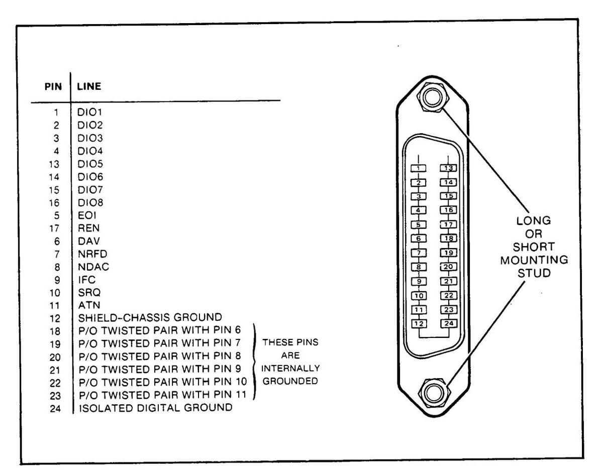
Figure 2-2. Hewlett-Packard Interface Bus Connection
2-17. The HP-IB cables have identical "piggy-back" connectors on both ends so that several cables can be connected to a single source without special adapters or switch boxes. System components and devices may be connected in virtually any configuration desired. There must, of course, be a path from the calculator (or controller) to every device operating on the bus. As a practical matter, avoid stacking more than three or four connectors on any one connector. If the stack gets too large, the force on the stack produces great leverage which can damage the connector mounting. Be sure each connector is firmly (finger tight) screwed in place to keep it from working loose during use.
2-18. CABLE LENGTH RESTRICTIONS. To achieve design performance with the HP-IB, the proper voltage levels and timing relationships must be maintained. If the system cable is too long, the lines cannot be driven properly, and the system will fail to perform properly. Therefore, when interconnecting an HP-IB system, it is important to observe the following rules:
- a. The total cable length for the system must be less than or equal to 20 metres (65.6 feet).
- b. The total cable length for the system must be less than or equal to 2 metres (6.6 feet) times the total number of devices connected to the bus.
- c. The total number of instruments connected to the bus must not exceed 15.
2-19. HP-IB TALK/LISTEN AND ADDRESS SWITCHES
2-20. The HP 5345A provides a rear panel HP-IB TALK/LISTEN selection switch. This switch determines the mode of remote operation as "Talk Only" or "Addressable".
2-21. The ADDRESS switches on the counter rear panel are used to manually set the remote control address of the counter. The addresses 20 and 21 are reserved for the controller, and only even numbered addresses may be programmed because the counter A1 bit has been internally tied low. Odd numbered addresses are used to access computer dump mode which will be discussed in Section III.
2-22. HP-IB DESCRIPTIONS
2-23. A description of the HP-IB is provided in Section III of this manual. A study of this information is necessary if the user is not familiar with the HP-IB concept. Additional information concerning the design criteria and operation of the bus is available in IEEE Standard 488-1978, titled "IEEE Standard Digital Interface for Programmable Instrumentation" .
2-24. REPACKING FOR SHIPMENT
2-25. If it becomes necessary to reship the counter, good commercial packing should be used. Contract packaging companies in many cities can provide dependable custom packaging on short notice. Instruments should be packed securely in a strong corrugated container (350 lb./sq. inch bursting test) with suitable filler pads between the instrument and container. The 4-corner support is not adequate, the counter must also have center support. Before returning instruments to Hewlett-Packard, contact the nearest Hewlett-Packard Sales and Service Office for instructions.
2-26. ENVIRONMENT DURING STORAGE AND SHIPMENT
2-27. Conditions during storage and shipment should normally be limited as follows:
- a. Maximum altitude: 25,000 feet.
- b. Minimum temperature: -40°FF (-40°C).
- c. Maximum temperature: +167°F (+75°C).
SECTION III OPERATION AND PROGRAMMING
3-1. INTRODUCTION
3-2. Section III contains operating and programming information that is helpful in realizing the best performance from the instrument. This includes a general description of the operating modes, the function of controls and indicators, operator's maintenance, a self-check procedure, setup procedures for making basic measurements, and remote programming instructions.
3-3. MEASUREMENT TECHNIQUE
3-4. The counter uses a period average technique to make measurements. The counts (or pulses) that are generated from the input and time base signals are collected in separate scalers during the measurement time. The counter compares these pulses arithmetically and displays the result on the front panel.
3-5. OPERATING MODES
3-6. The following paragraphs describe the operating modes for frequency, period, time interval, ratio, and totalize measurements.
3-7. Frequency Mode
3-8. Channel A accepts input frequencies from 50 µHz to 500 MHz with a minimum level of 25 mV rms sine wave. These frequencies are counted directly with no prescaling techniques applied. Extended frequency capability is available with the use of plug-ins. The counter is capable of measuring pulsed RF in either a single burst or an average of several bursts. The measurement time within the burst may be varied in length and position for detecting frequency variations within a burst.
3-9. The measurement time is the selected gate time plus the time until the next trigger pulse occurs. For example, if the selected gate time is 1 ms, the event gate will close on the next trigger after 1 ms has elapsed. If the input frequency were 20 kHz (.05 ms period), the measurement time would be 1 ms + .05 ms = 1.05 ms. The difference encountered does not affect the accuracy of the measurement.
3-10. Period Modes
3-11. Two modes of period measurements are available: single period and period average. These modes are described in the following paragraphs.
3-12. SINGLE PERIOD. Single period measurements are made with with the GATE TIME switch set to MIN. In this position, the gate time is one period or 50 ns, whichever is greater. Therefore, the input frequency range for a single period measurement is 50 µHz to 20 MHz. Frequencies greater than 20 MHz may be applied, but they will be averaged during a 50 ns gate time.
3-13. PERIOD AVERAGE. When the GATE TIME switch is set to any other position than MIN, the counter averages multiple periods. Averaging increases the accuracy and resolution of the measurement. Input frequencies are in the 50 µHz to 500 MHz range. The actual gate time is determined in the same manner as that described under Frequency Mode.
3-14. Number of Periods Averaged. To determine the number of periods averaged during a measurement, divide the displayed answer into the selected gate time.
Example: Gate Time setting (sec) =
The number of periods averaged will always be a whole number. Therefore, should the calculated answer contain any digits to the right of the decimal point, drop these digits and increment the remainder by one. This is due to the extended gate time. The answer for this example, then, is 49 periods averaged.
3-15. Time Interval Modes
3-16. The counter measures time intervals from Channel A to Channel B; that is, Channel A starts the measurement and Channel B stops the measurement. Time between points on a single waveform can be measured by connecting the input signal to CHANNEL A jack and placing the Input Amplifier Control switch to COM A. Under these conditions, the slope and level controls of Channel A and Channel B allow variable triggering on either the + or - slope. With the Input Amplifier Control switch set to SEP, measurements can be made between points on separate waveforms.
3-17. SINGLE TIME INTERVALS. Single time intervals down to 10 ns are measured with the GATE TIME switch set to MIN. The gate time is one time interval for repetition rates of less than 20 MHz. Thus, if two or more time intervals occur within 50 ns, they will be averaged.
3-18. TIME INTERVAL AVERAGE. The counter averages multiple time intervals when the GATE TIME switch is set to any position other than MIN. The maximum repetition rate is 50 MHz (10 ns time interval plus 10 ns deadtime = 20 ns period or 50 MHz). To average, the time interval must be less than the selected gate time.
NOTE
If the time interval is greater than the gate time, but not more than 3.5 times greater, a single period will be measured. The MIN gate time position is preferred for single periods.
3-19. When averaging, white noise modulates the internal clock signal to prevent any harmonic relationship between the input signal and the clock. This increases the measurement accuracy. The noise is not generated when the GATE TIME switch is set to MIN.
3-20. INITIATING A MEASUREMENT. The front-panel ARM and GATE lights and the rearpanel dc trigger levels are helpful when setting up a time interval measurement. Place the GATE TIME switch to 100 µs. The ARM light is an indication that Channel A is not triggering, possibly due to insufficient signal amplitude or misadjusted front-panel controls. A flashing GATE light indicates that Channel A is triggering. If the counter is gating and lamp test (paragraph 3-63) is flashing or appears to be steady, the counter has gone into excessive gate time (paragraph 3-36). This means the counter has reset because Channel B was not triggered with a stop signal. This could be caused by the stop pulse failing to arrive until after the maximum allowable time, which is 3.5 times the selected gate time. In this case, increase the gate time. Other causes could be insufficient signal amplitude or misadjusted front-panel controls.
3-21. MEASUREMENT TIME. In time interval average, the time needed to complete a measurement may be much longer than the selected gate time. This is because the counter collects a gate time's worth of time intervals . The factors which would increase the measurement time are short time intervals and extended time between intervals (see Figure 3-1).
3-22. Occasionally, when increased resolution is needed, it may be convenient to estimate the total time of a measurement. To calculate this, use the equation below.
| Measurement | Time = | Gate Time (sec) | ||||
|---|---|---|---|---|---|---|
| Time Interval (sec) X Number of Time Intervals per sec | ||||||
| Example: | 1 msec | =_ | 1 X 10 -3 sec | = 12.5 seconds | ||
8 X 10⁻⁵
100 ns X 800/sec
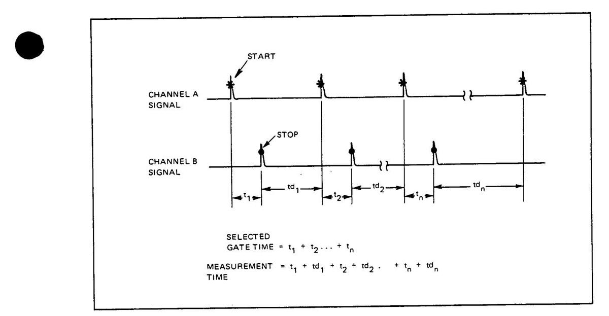
Figure 3–1. Measurement Time for Time Interval Average
3-23. If the time interval used in the equation is unknown, it can be obtained from the counter by selecting MIN. The number of time intervals per second can be taken from an oscilloscope reading. For most purposes, these figures need be only approximate to give a reasonable indication of the waiting time involved.
3-24. Ratio Measurements
3-25. The ratio between two frequencies (FB/FA) is measured by connecting one signal to Channel A and the other to Channel B. Both channels operate in the 50 µHz to 500 MHz range. If the higher frequency is connected to Channel B, the ratio will be greater than one. The answer for a ratio measurement is a unitless figure.
3-26. MEASUREMENT TIME. The difference between the selected gate time and the total measurement time depends on the frequency applied to Channel B. In the Ratio mode, the Channel B signal substitutes for the internal 500 MHz time base.
3-27. With the GATE TIME switch set to 1 s, for example, 5 X 10⁸ time base counts are needed to end the measurement. When the 500 MHz internal time base is used, the 5 X 10⁸ counts are accumulated in 1 second. If, for example, 70 MHz were applied to Channel B and used as the time base, it would take about 7 times as long (7.14 seconds) to accumulate the 5 X 10⁸ counts needed to disarm the gate.
3-28. To estimate the measurement time, use the equation below.
Measurement Time = 5 X 10⁸ Hz X Gate Time Channel B Freq.
Example: 5 X 108 Hz X 1 ms = 5 X 108 X 1 X 10-3 sec = 20 ms

3–3
3-29. Totalize Mode
3-30. The START and STOP positions on the FUNCTION switch allow manual opening and closing of the counter's main gate. The Input Amplifier Control switch must be placed in SEP. When the switch is in the START position, the counter totalizes the number of times the input signal passes through the Channel A trigger point. The GATE TIME switch does not affect the displayed result in any way.
3-31. BOTH CHANNELS TOTALIZED. When the Input Amplifier Control switch is set to SEP, Channel A and Channel B signals can be totalized simultaneously. The displayed result is a function of the ACCUM MODE START/STOP switch, located on the rear panel. The two signals are added (A+B) or subtracted (A-B), depending on the switch position. When the Input Amplifier Control switch is set to CHECK, the counter always selects A+B.
3-32. A minus sign on the display indicates that during a subtraction (A-B) the B events have outnumbered the A events. With the switch in A-B, the instrument functions like an up-down or reversible counter. That is, the counter will count down from a previously-given positive number. As an example of this, assume that the A frequency is greater than the B frequency and the switch is in A-B. The display accumulates positive numbers at a rate equal to the difference between the two input frequencies. If the frequency of B now becomes greater than A, the displayed count will decrease towards zero, again, at a rate equal to the difference between the two frequencies. Once the declining number passes through zero, the minus sign lights and the display continues to accumulate.
3-33. SCALED OUTPUT. With the FUNCTION switch set to START and SAMPLE RATE to HOLD, the counter scales (divides) the Channel A input frequency by powers of 10. This scaled signal is available on the rear-panel CHAN A SCALER OUTPUT jack. Although the display is not functioning, the counter is accumulating. The GATE TIME switch controls the division factor, as shown in Table 3-1.
| GATE TIME SETTING | SCALING FACTOR | SCALED OUTPUT (100 MHz IN OR CHECK) |
|---|---|---|
|
100 ns
1 μs 10 μs 100 μs 1 ms 10 ms 100 ms 1 s 100 s 1000 s |
10
2
10 3 10 4 10 5 10 6 10 7 10 8 10 9 10 10 10 11 10 12 |
1 MHz
100 kHz 10 kHz 1 kHz 100 Hz 10 Hz 1 Hz 100 mHz 10 mHz 1 mHz 100 μHz |
Table 3-1. Scaler Output for Channel A
3-34. INPUT TRIGGERING
3-35. The input circuits provide triggering over a range of -2.0V to +2.0V. The point at which triggering occurs is adjustable with the front-panel LEVEL control. Each input channel has a small amount of hysteresis (about 10 mV). If the SLOPE switch is set to "+," the trigger pulse occurs at the top of the hysteresis window . If the SLOPE switch is set to "-," the pulse occurs on the bottom line of the window. In other words, the signal must pass through the entire hysteresis window before a trigger pulse is generated (see Figure 3-2). The LEVEL control must be placed to allow at least a 1 ns pulse width for the Schmitt Trigger.
Figure 3-2. Internal Triggering
3-36. EXCESSIVE GATE TIME
3-37. In every measurement involving a gate time, the counter depends on the input signal to terminate the measurement. The measurement concludes one clock pulse after the next input pulse following the end of the gate time, not with the gate time itself. If the period of the input signal is much longer than the gate time or if the signal is interrupted sometime during the gate time, the excessive gate time circuits prevent the counter from waiting indefinitely for the terminating pulse. The counter will wait for about 3.5 times the selected gate time before resetting. At the end of excessive gate time, the display will flash instantaneously to lamp test before displaying all zeros. Excessive gate time is especially useful during the time interval measurement; see paragraph 3-20 for a further description.
3-38. EXTERNAL ARMING AND GATING
3-39. The GATE CONTROL INPUT jack (rear panel) allows the counter to be externally armed and gated. The jack works in conjunction with the Gate Control switch, located directly below the jack.
3-40. External Arming
3-41. When externally arming, set the Gate Control switch to EXT ARM and the SAMPLE RATE switch to HOLD. The counter will ARM when the instrument is first turned on because of the internal arming of the sample rate circuits. After the first measurement, however, the counter's arming circuits are fully controlled by the external source. The counter is armed within 1 µs of receiving the arm pulse (500 ns to dc at -1V). Once the counter is armed, the measurement begins with the first Channel A trigger pulse. The counter makes only one measurement for each arm pulse.
3-42. External Gating
3-43. When the Gate Control switch is set to EXT GATE, the counter's arming and gating is under full external control. The gating can be accomplished in two ways: single gating or multiple gating.
3-44. SINGLE PULSE GATING. Single gating is accomplished with a single, external gate pulse. The width of this pulse can be varied from 20 ns to 20,000 seconds. When using a single gate, set the GATE TIME switch to MIN. This assures the measurement will always take place during a single, external gate pulse. This will not be true for other settings of the GATE TIME switch.
3-45. MULTIPLE PULSE GATING. This method requires an arming pulse, which is automatically taken from the external gate pulse train. When the GATE TIME switch is in any position other than MIN, the counter accumulates as many external gate pulses as are needed to equal or exceed the gate time selected by the switch. As an example, assume a GATE TIME setting of 10 ms and external gate pulses of 4 ms. The counter requires three of these pulses before a measurement can be completed. The total gate time is 12 ms.
3-46. One of the uses of multiple gating is frequency averaging , i.e., an average of frequency measured over multiple bursts. Using the same values as above, Figure 3-3 shows the type of gating in frequency averaging.
Figure 3-3. Multiple Gating
3-47. Time Interval Measurements
3-48. External gating is valuable when measuring the time between two events while ignoring the events occurring between them. The external gate signal must go low (-1 V) before the start pulse and return high (0 V) before the stop pulse.
3-49. SINGLE TIME INTERVALS. As previously mentioned for external gating, a measurement using a single external gate requires the GATE TIME switch to be set to MIN. The counter arms automatically and the external gate pulse provides a control over the time interval measurement. Varying the width of the pulse determines which time interval is measured, as can be seen in Figure 3-4.
Figure 3-4. External Gating for Single Time Interval
3-50. MULTIPLE TIME INTERVALS. An average of time intervals can be measured using the external gating method. This method, as in single time intervals, allows certain pulses of the waveform to be ignored. The GATE TIME switch must be set to any other position than MIN. See Figure 3-5 for an example of time interval averaging. This method does require an arming pulse for each measurement cycle.
Figure 3-5. External Gating for Time Interval Averaging
3-51. DISPLAY
3-52. The counter uses a 12-digit display: 11 digits of data and 1-digit for the minus sign. Unlike most counters, the number of digits displayed in a measurement is not a function of the input frequency and is not related to the FUNCTION switch. The number of digits is constant for each setting of the GATE TIME switch.
3-53. Display Position
3-54. When the DISPLAY POSITION switch is set to AUTO, the counter automatically positions the display's least-significant digit in the right-most column. Rotating the switch to each of its counterclockwise positions (blue dots) shifts the decimal point, hence the display, one place to the left. Once the switch is placed to any position other than AUTO, the annunciator (k, M, n, etc.) stays fixed, regardless of changing input frequency. The annunciator remains fixed until the RESET button is pushed or the FUNCTION switch setting is changed. Manually fixing the decimal point and the annunciator is convenient when collecting measurement data with a digital-to-analog converter. As an example, the DAC can continually record any 3 digits in a possible display of 11, regardless of changing input data.
3-55. Asterisk
3-56. The asterisk lamp will light under any one of four conditions: overfow, underflow, factitious zeros, or insuffucient oven temperature (standard only). Overflow occurs when the placement of the DISPLAY POSITION switch has positioned the display's most-significant digit(s) so far to the left that it is out of viewable range. Underflow occurs when the placement of the DISPLAY POSITION switch has positioned the display's least-significant digit(s) so far to the right that it is out of viewable range. If the counter is equipped with an oven-controlled oscillator (standard), the operating temperature of the oven must remain constant for the crystal to perform properly. Should the oven temperature drop below its normal operating range, the asterisk light will come on as an indication of this condition.
3-57. Factitious zeros occur when the settings of the GATE TIME switch and DISPLAY POSITION switch has been combined to give fewer significant digits than the DISPLAY POSITION demanded. In this combination, the display attempts to blank one or more of the significant digits located to left of decimal point. Instead of blanking the digit, the display substitutes an artificial and meaningless zero to keep that portion of the display filled.
3-58. Although the presence of factitious zeros is a rare occurrence, its appearance can be demonstrated with the counter set-up as follows: FUNCTION to FREQ A, connect input signal of 125 MHz, turn DISPLAY POSITION switch out of AUTO to about mid-range, turn GATE TIME switch ccw until the display is 125 MHz. The next switch position changes the display to 120 MHz and lights the asterisk. The zero now displayed is a factitious or filler zero.
3-59. Arm Light
3-60. An illuminated ARM light indicates that Channel A is not triggering. The condition of this indicator should be observed when adjusting the front-panel controls for a first-time measurement. Insufficient amplitude of the input signal or improper setting of the input controls (LEVEL, ATTEN, etc.) are common causes for the failure of the GATE light to turn on.
3-61. Gate Light
3-62. Once Channel A triggers, the ARM light turns off and the GATE light turns on. The GATE indicator lights during the time the counter's event gate is open. For short-duration gate times, the GATE light circuits include a 40 ms one-shot mV to allow a visible flash of the lgiht. The SAMPLE RATE control sets the time between flashes (or measurement cycles).
3-63. Lamp Test
3-64. To ensure that all segments of the display are capable of lighting, the counter provides a lamp test. The display should appear like the representation shown on the next page (Figure 3-6).

3-65. Lamp test occurs under several conditions:
- a When the RESET button is pushed.
- b. When the POWER switch is placed to ON, lamp test will light for about 2 seconds.
- c. When switching between detent positions of the GATE TIME switch, FUNCTION switch, or DISPLAY POSITION switch.
- d. When counter is attempting to phase lock the internal oscillator to an external standard.
- e When the counter has gone into excessive gate time.
- f. When operating with an external frequency standard (rear panel INT STD-EXT STD set to EXT STD) and the external frequency is lost or disconnected.
3-66. COOLING
3-67. The counter's fan, located behind the display assembly, provides forced-air cooling to the electronic components throughout the instrument. The fan takes air in through the left side panel and bottom cover and exhausts it through the top cover and right side cover via the plug-in compartment.
NOTE
Check for proper air flow each time the instrument is turned on. If the unit is operated for extended periods of time without adequate cooling, the counter will automatically turn off.
3-68. AIR FILTER CLEANING
NOTE
Instruments with serial number 1708A02576 or higher are supplied less the air filters. Hewlett-Packard recommends removing the filters from all previous units. If desired to retain the filter protection, follow the step-by-step instructions below.
3-69. When the instrument is placed into service, the air filters should be inspected frequently to determine the rate at which they collect dirt in their particular environment. Under average conditions, the air filters should be cleaned about every 3 months. To remove these filters, proceed as follows:
- a. Remove power cord at rear panel.
- b. Remove the top and bottom covers (4 screws each).
- c. Remove the 4 screws holding in display assembly (see Figure 3-7). Remove display assembly from mainframe and disconnect its power cable at bulkhead.
- d. Remove left-front side cover (4 screws).
- e. On left side frame, remove right-most top and bottom screws (1 ea.) and extract side air filter.
- f. Remove the 4 screws holding the 2 internal brackets and extract bottom air filter.
Use the following procedure to clean the air filters.
- a. Wash air filters with water.
- b. Let stand until completely dry.
- c. Recoat filters with RP Super Filter Coat Adhesive, Research Products Corporation.
Figure 3-7. Location of Display Assembly Screws
Figure 3-8. Removal of Display Assembly
Figure 3-9. Location of Air Filters
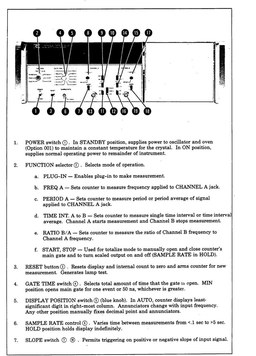
- 8. LEVEL control (i) (j). Used in conjunction with ATTEN switch to select voltage at which triggering occurs. With X1 attenuator setting, level is variable ±2.0V; on X10, ±20V.
- 9. Input Impedance switch ③ ④. Selects input impedance to 50Ω or 1 MΩ shunted by approximately 45 pF.
- 10. ATTEN switch (1) (5). Selects attenuation for input signal. Used in conjunction with LEVEL control to set trigger point. Input level is not affected in X1 position. Signal amplitude is reduced by factor of 10 in X10 position.
- 11. Coupling switch (1) (6). Selects direct or capacitor coupling for input signal.
-
12. Input Amplifier Control switch 12.
- a. CHECK Checks that counter is functioning properly by connecting internal 100 MHz test signal to Channel A and B.
- b. COM A Operationally connects A and B channels in parallel. Used for single source time interval measurements. Channel B jack is not active. Channel A and B Input Impedance switches must be set to same position.
- c. SEP Allows independent operation of Channel A and B.
- 13. Input jacks (1) (1). Inputs for Channel A and Channel B. Each input can accept signals from 50 µHz to 500 MHz.
Figure 3-10, Front Panel Controls and Connectors (Continued)
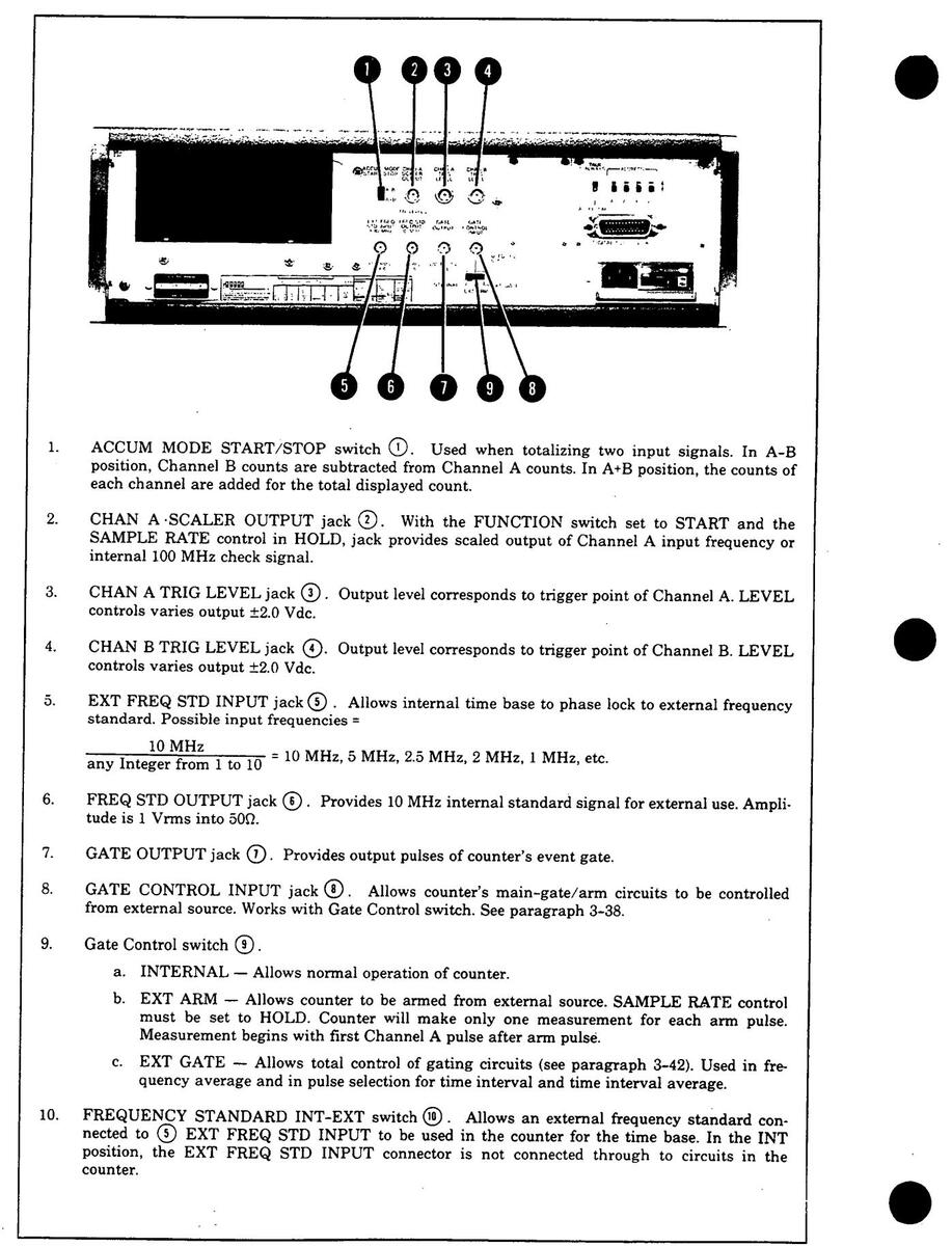
Figure 3-11. Rear Panel Controls and Connectors
Table 3-2. Self Check
1. Set the counter controls as follows:
Input Amplifier Control switch to CHECK. FUNCTION switch to PLUG-IN. GATE TIME switch to MIN. DISPLAY POSITION switch to AUTO. SAMPLE RATE control to maximum ccw.
- 2. Turn POWER switch to ON. Check that the counter displays a minus sign and eleven 7-segment symbols ( 2/2) with 11 decimal points. This display should last about 2 seconds before switching to 11 zeros with no decimal points.
- 3. Set FUNCTION switch to FREQ A. The GATE light should be flashing.
- 4. Set GATE TIME switch as shown in table below, and check for proper display.
| GATE TIME | DISPLAY | ANNUNCIATOR |
|---|---|---|
|
MIN
100 ns 1 μs 10 μs 100 μs 1 ms 10 ms 100 ms 1 s 100 s 100 s 1000 s |
.1
.10 100. 100.0 100.00 100.000 100.0000 100.00000 100.000000 100.000000 00.00000000 |
G Hz
G Hz M Hz M Hz M Hz M Hz M Hz M Hz M Hz M |
5. Set FUNCTION switch to PERIOD A and then to TIME INT. A to B. Check for proper display, as shown in the table below.
| GATE TIME | DISPLAY | ANNUNCIATOR |
|---|---|---|
|
MIN
100 ns 1 μs 10 μs 100 μs 1 ms 10 ms 100 ms 1 s 10 s 100 s 1000 s |
10.
10. 10.0 10.00 10.000 10.00000 10.000000 10.0000000 10.0000000 10.00000000 |
n sec
n sec n sec n sec n sec n sec n sec n sec n sec n sec n sec n sec n sec n sec n sec |
- 6. Set FUNCTION switch to RATIO.
- 7. Set GATE TIME switch as shown in table below, and check for proper display.
| GA | TE TIME | DISPLAY | |||||
|---|---|---|---|---|---|---|---|
| .* |
MIN
100 ns 1 μs 10 μs 100 μs 1 ms 10 ms 100 ms 1 s 10 s 100 s 000 s |
1
1.0 1.00 1.000 1.0000 1.000000 1.0000000 1.00000000 |
)
) ) ) ) ) * |
||||
| 8. |
Set FUNCTIC
light is on. |
ON switch | to START. Check | that counter totali | zes and | that the GATE | |
| 9. | Set FUNCTIO | ON switch | to STOP. Check t | hat GATE light goo | es out a | nd the display is | |
| 10. |
Set FUNCTIC
previously hel |
ON switch i
d number. |
to START. The co | ounter should begin | totalizi | ng from the | |
| 11. |
Set FUNCTIO
100.00 MHz. |
ON switch 1 | to FREQ A and G | ATE TIME switch | to 100 µ | us. Display is now | |
| 12. |
Turn the DISI
proper display |
PLAY POS
7, as shown |
ITION switch (blu
i in the table below |
ie knob) through it:
v. |
s positic | ons and check for | |
| D | DISPLAY POSI | FION | DISPLAY (X | = BLANK) | ANN | IUNCIATOR | |
|
AUTO
100 s 10 s 1 s 100 ms 10 ms 1 ms 100 μs 10 μs 1 μs 100 ns MIN |
XXXXXX
XXXXXXX XXXXXXX XXXXXXX XXXXX100 XXX100.00 XX100.00X 100.00XX 00.00XXX 0.00XXXX |
100.00
KX100. X100.0 100.00 00.00X .00XX 0XXX XXXX X |
M Hz
*M Hz *M Hz M Hz M Hz M Hz M Hz M Hz M Hz M Hz |
||||
| 13. | Push RESET |
button. Cł
) with 11 de |
neck that counter of ecimal points. | lisplays a minus si | gn and d | eleven 7-segment | |
Table 3-2. Self Check (Continued)
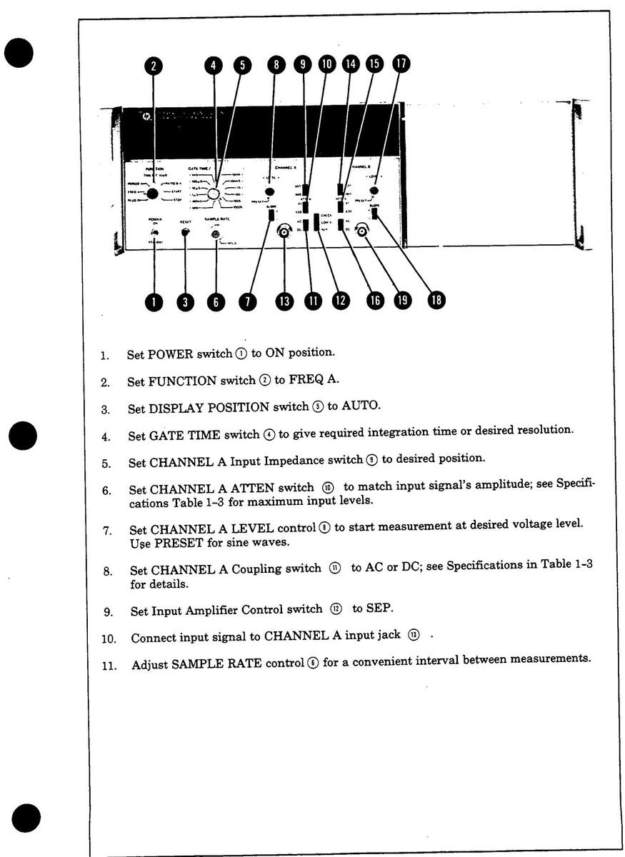
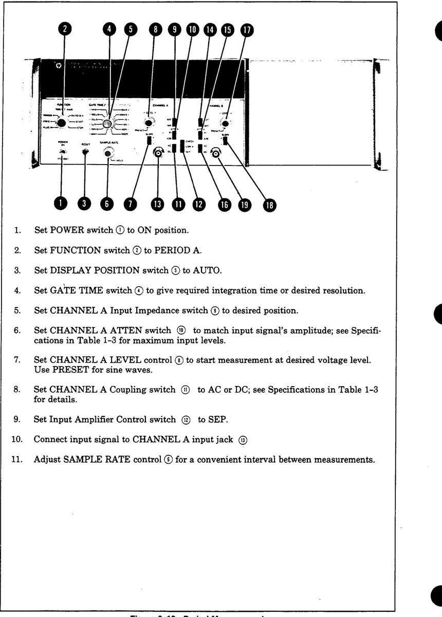
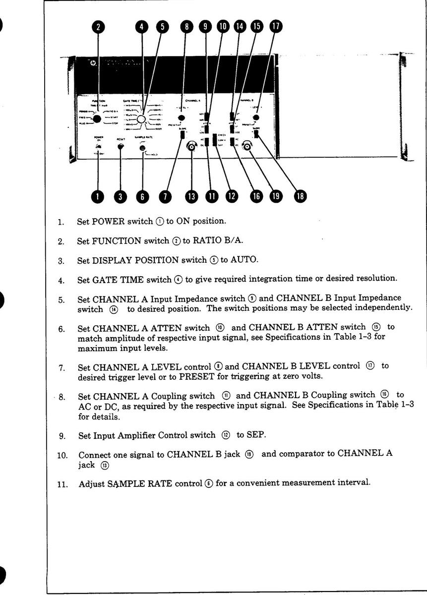
Figure 3-14. Ratio Measurements
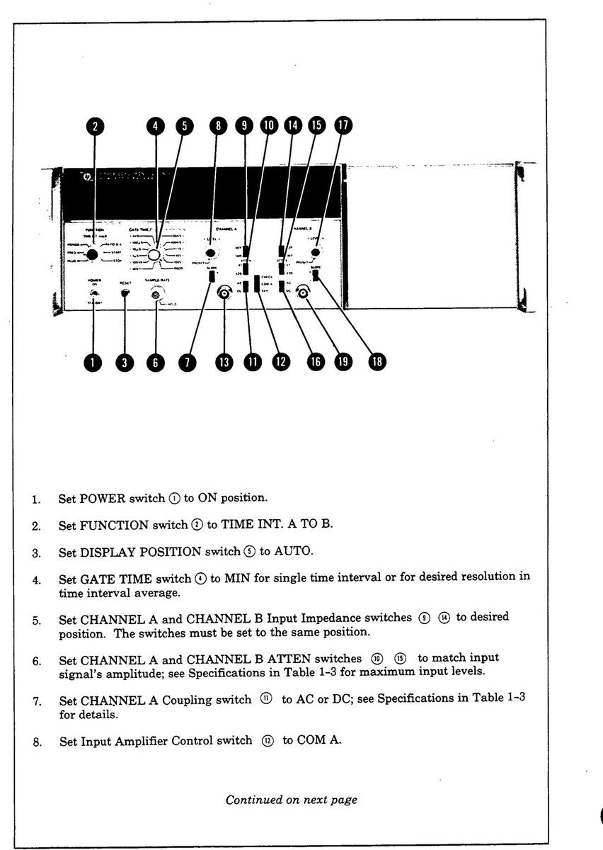
Figure 3-15. One Source Time Interval Measurements
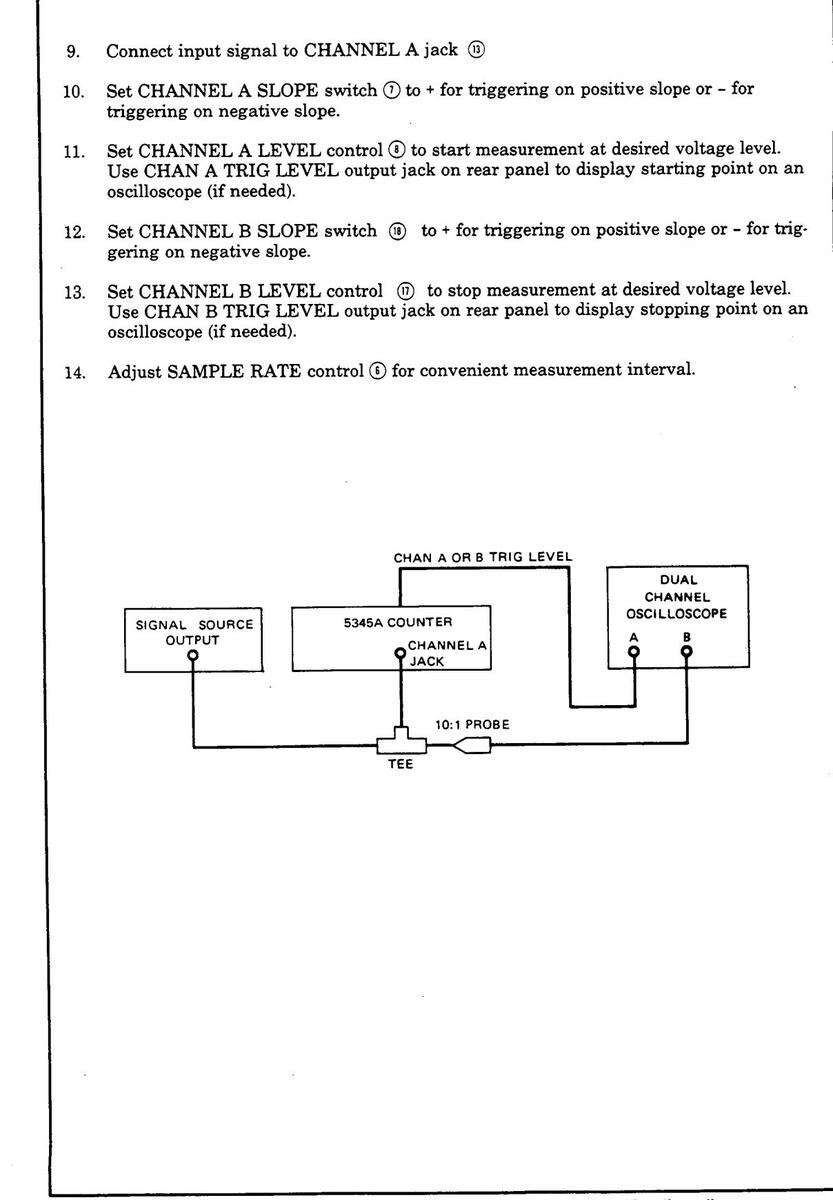
Figure 3-15. One Source Time Interval Measurements (Continued)
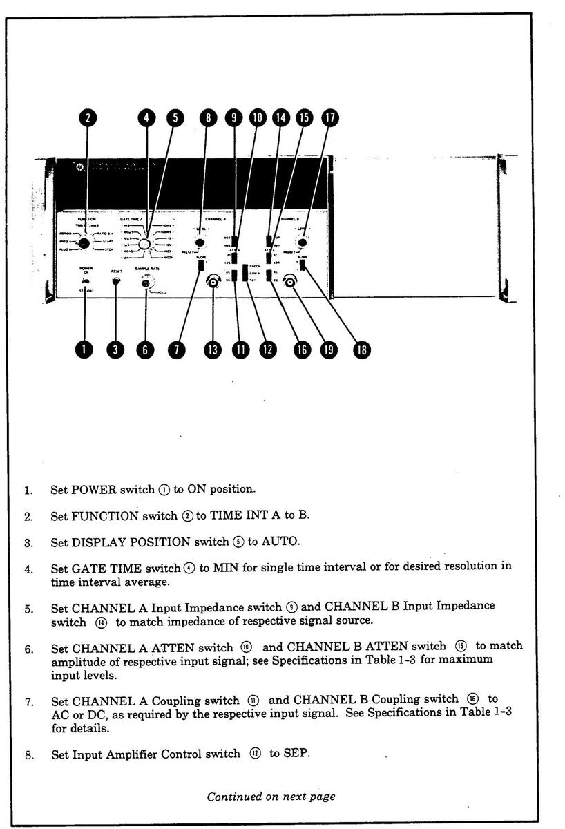
Figure 3-16. Two Source Time Interval Measurements

- 10. Set CHANNEL A SLOPE switch ① to + for triggering on positive slope or to for triggering on negative slope.
- 11. Set CHANNEL A LEVEL control (1) to start measurement at desired voltage level. Use CHAN A TRIG LEVEL output jack on rear panel to display starting point on an oscilloscope (if needed).
- 12. Set CHANNEL B SLOPE switch (1) to + for triggering on positive slope or for triggering on negative slope.
- 13. Set CHANNEL B LEVEL control (1) to stop measurement at desired voltage level. Use CHAN B TRIG LEVEL output jack on rear panel to display stopping point on an oscilloscope (if needed).
- 14. Adjust SAMPLE RATE control (6) for a convenient measurement interval.
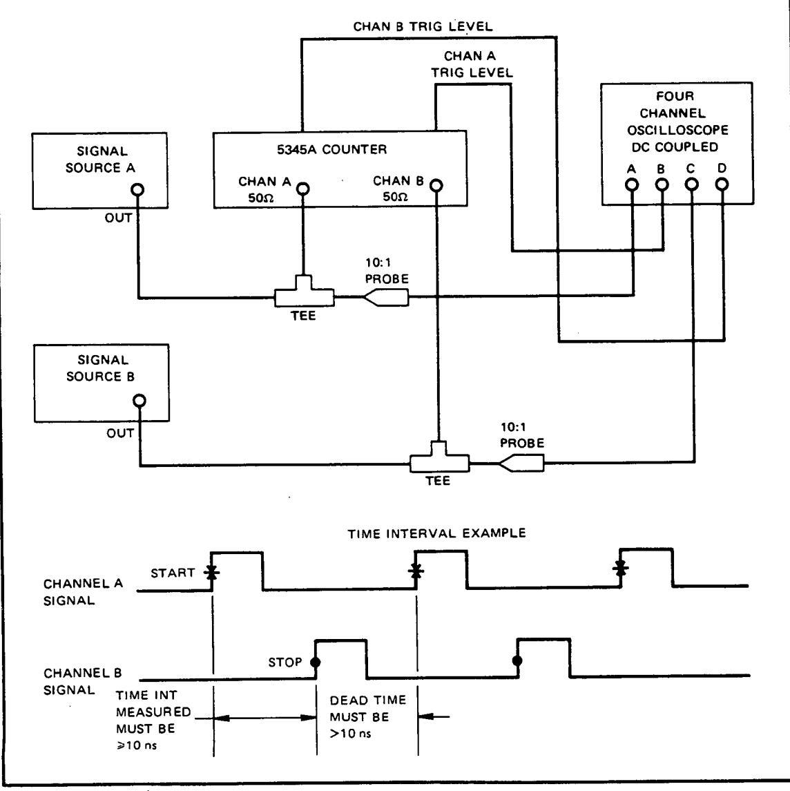
Figure 3-16. Two Source Time Interval Measurements (Continued)
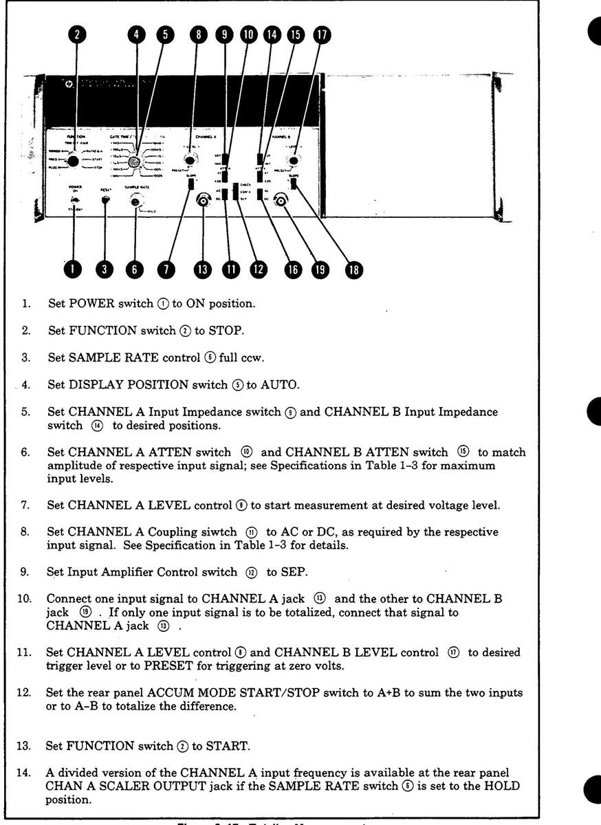

3-70. REMOTE PROGRAMMING VIA THE HEWLETT-PACKARD INTERFACE BUS
3-71. Introduction
3-72. The Hewlett-Packard Interface Bus (HP-IB) is used to transfer data and instrument control instructions between devices. Such devices include measurement instrumentation, programmable signal generators, printers, plotters, and computers to name a few. By connecting these various devices together via the HP-IB, systems ranging from extremely simple to highly complex may be assembled.
3-73. To remotely program the counter efficiently, the operator must be familiar with the selected controller, the configured interface, and the manual operation and functional capabilities of the 5345A. The following HP manuals should provide useful background information:
Hewlett-Packard BASIC 3.0 Interfacing Techniques for HP 9000 Series 200 Computers Hewlett-Packard Tutorial Description of the Hewlett-Packard Interface Bus
3-74. Interface System Terms
-
3-75. The following paragraphs define terms and concepts used to describe HB-IB system operations.
- a. Address: Each device on the interface is assigned an address. The address is used to specify which device will receive or send information.
- b. Byte: A byte is a unit of information consisting of eight binary digits called bits.
- c. Device: Any instrument or unit that is HP-IB compatible is called a device.
- d. Device Independent Command: A command predefined by the interface standard to have a specified bit pattern, and resulting action.
- e. Device Dependent Command: A command that is specific to a particular instrument or family of instruments, which are not predefined by the interface standard. Device dependent commands are usually sent as ASCII strings of characters.
-
f. Polling: Polling is a process used by a controller to obtain device status information. Polling can be conducted by the controller at any time, however, typically the polling sequence is initiated when a device has requested service. The HP-IB has two types of polling: Parallel Poll and Serial Poll. Parallel Poll is not supported by the 5345A. Serial Poll is only supported by Option 012.
- 1. Parallel Poll: Parallel Poll is used to simultaneously gather the status of several devices connected to the bus. When the controller executes a Parallel Poll, each device selected sends one bit of (either True or False) status information.
- 2. Serial Poll: When the controller executes a Serial Poll, the addressed device sends one byte of operational information called a status byte. If the controller has enabled Serial Poll in response to a service request and there is more than one device capable of requesting service, the controller must Serial Poll each device individually to determine which device requested service. When an Option 012 5345A is Serial Polled, its status byte will contain 01000000 (ASCII "1") if it has enabled service request (SRQ), and 00000000 (ASCII "NUL") if it has not enabled SRO.
Since Option 011 does not respond to Serial Poll, the controller must address each Option 011 counter individually to TALK mode in order to determine which Option 011 5345A requested service. Only the counter with output information will respond. This method may also be used with Option 012.
3-76. HP-IB Description
3-77. The Hewlett-Packard Interface Bus is a high speed parallel interface bus. All devices on the bus are capable of being addressed at one time. However, only one device may respond at a time. The controller is used to address devices, and maintain orderly data flow to and from the devices.
3-78. Each device on the interface may have one or more of the following capabilities: Controller, Talker, or Listener. The controller has the responsibility of controlling interface activity, and must be equipped with
the proper interface module. Controllers transmit all device independent commands to other devices in the interface and usually have Talker and Listener capabilities. Only one device on the interface may be the active controller at any one time. The 5345A Electronic Counter has no controller capabilities.
3-79. The HP-IB system uses a party-line structure (devices share signal lines) on which a maximum of 15 devices (including the controller) may be connected in virtually any configuration desired - as long as there is an uninterrupted path from the controller to every device operating on the bus.
3-80. The bus is made up of 16 signal lines, and 8 ground lines. Of these 16, 8 are data lines, 5 are HP-IB control lines, and 3 are data transfer control lines.
3-81. The eight data lines are used to transfer ASCII data from one instrument to another. 'These lines are labeled DI01 through D108.
3-82. The five HP-IB control lines are used to maintain an orderly flow of data across the HP-IB. These lines are labeled:
- a. SERVICE REQUEST (SRQ)
- b. REMOTE ENABLE (REN)
- c. INTERFACE CLEAR (IFC)
- d. ATTENTION (ATN)
- e. END OR IDENTIFY (EOI)
3-83. The three transfer control lines are used to transfer each byte of data using what is known as the three-wire handshake. These lines are labeled:
- a. NOT READY FOR DATA (NRFD)
- b. DATA VALID (DAV)
- c. NOT DATA ACCEPTED (NDAC)
3-84. HP-IB Control Lines
a. SERVICE REQUEST (SRO)
When a device requires interaction with the controller, it enables the SRQ line which sends a request to the controller for attention. When the controller is ready, it will service the device.
Option 011 and Option 012 enable SRQ if the 5345A output mode is programmed to "WAIT Until Addressed" and a completed measurement is ready for output. Service Request is disabled at all times if the 5345A output mode is programmed to output "ONLY IF Addressed".
- b. REMOTE ENABLE (REN)
- c. The Remote Enable line is used to instruct devices to enter into remote mode and thus, accept data and programming information sent over the HP-IB.
Option 011 responds to the REN signal only if its remote-local storage cell has been properly programmed. The remote-local storage cell has two states: Switch to Local and Switch to Remote. Switch to local is selected by sending the ASCII characters EO. Switch to Remote is selected by sending the ASCII characters E8. The 5345A will enter remote mode if it is programmed for "Switch to Remote" and the REN line is asserted. It will enter local mode (in which the instrument is set by the front panel controls) if the REN line is not asserted or the counter is programmed for "Switch to Local".
Option 012 responds to the REN signal at all times. Thus, if REN is asserted, the 5345A will be in remote mode. If REN is not asserted, the counter will be in local mode.
c. INTERFACE CLEAR (IFC)
Only the controller can set the IFC line true. By asserting IFC, all bus activity is unconditionally terminated, and any current talkers and listeners become unaddressed.
Option 011, and Option 012 respond and monitor IFC at all times. When IFC is asserted, the 5345A will immediately stop driving the data and transfer lines. The SRQ line, however, will not be affected by IFC, and thus, will not be cleared if it had previously been asserted by the 5345A.
d. ATTENTION (ATN)
The ATN line is used to differentiate between data and bus instructions. If ATN is asserted, information on the data lines should be interpreted as a bus instruction. If ATN is not asserted, information should be interpreted as data.
Option 011, and Option 012 respond and monitor ATN at all times. When ATN is not asserted, the 5345A will output its data if it has been addressed to talk. When ATN is asserted, the 5345A will stop driving the lines and interpret the incoming data as bus commands.
e. END OR IDENTIFY (EOI)
Normally, data messages sent over the HP-IB are sent using standard ASCII code and are terminated by the ASCII character LF (line-feed). However, certain devices may wish to send blocks of information that contain data bytes which have the bit pattern of the line-feed character but are actually part of the data message. Thus, no bit pattern can be designated as a terminating character, since it could occur anywhere in the data stream. For this reason, the EOI line is used to mark the end of the data message.
The 5345A does not support the EOI feature.

3-85. HP-IB Transfer Control Lines
3-86. The three HB-IB transfer control lines and their interrelationship to each other during the three-wire handshake are as follows.
3-87. The transfer of a byte is initiated by the listener. When it is ready to accept data, it sets the Not Ready For Data (NRFD) line false. The talker then senses this condition, places a data byte on the bus, and sets the Data Valid (DAV) line true. When the listener senses DAV is true, it reads the data bus, and sets the Not Data Accepted (NDAC) line false, thus indicating that it has accepted the data byte.
3-88. Address Selection
3-89. Facing the rear panel of the counter, note the five slide switches above the HP-IB connector. The four rightmost switches (A5, A4, A3, A2) determine the counters Listen/Talk address. The far left switch is the Addressable/Talk Only switch. If the 5345A is to be connected to a printer only, with no controller on the bus, then set this switch in the Talk Only (up) position. If the bus has a controller then the 5345A must be able to respond to controller directives, and thus the Addressable/Talk Only switch must be set to the Addressable (down) position.
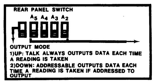
3-90. Only even addresses may be set on the 5345A, because the A1 switch is internally wired to the "0" position. However, the address corresponding to the A1 switch in the "1" position is also used by the 5345A, and thus, to prevent bus conflicts, both even and odd bus addresses must be reserved for the 5345A. The controller is typically set to address 21. Thus, the 5345A cannot be set to address 20, since it also requires address 21, which is already in use by the controller. Addresses 30 and 31 are also not allowed because 31 is reserved for the untalk and unlisten command. The programming examples at the end of this section were written with the counter set to address 18. It is therefore recommended that this address be used. To set the address to 18 position the switches as shown:
3-91. Addressing the 5345A for Talk and Listen
3-92. Addresses are communicated on the data lines. When the controller asserts ATN true, all 5345A's interpret the information on the data lines DI01 through D105 as an address if during this time, the signal levels on D107 and D106 are either "1" and "0", respectively, for a talker; or "0" and "1", respectively, for a listener.
NOTE
When the 5345A is addressed from a listener to a talker or talker to a listener, the appropriate clear codes ("?" or "-") must be issued.
3-93. Output Modes
3-94. The 5345A has two discrete output modes. It has a talk mode and a computer dump mode. The computer dump mode is used when it is desired to output 5345A readings at extremely fast rates or to analyze raw measurement data. The talk mode is used when there is enough time for the 5345A to calculate the measurement, and output the result.
3-95. Computer Dump
3-96. The 5345A will output in computer dump mode if it is addressed to talk, and its talk address is one higher than the address set on the rear panel. Thus, if the rear panel address setting is 18, the computer dump address would be 18+1=19-
3-97. When the 5345A is addressed to output in this mode, it will output the contents of the denominator (events) register and then output the numerator (time) register contents. The processing and display cycles within the 5345A are bypassed with this mode. The sample rate (wait time between measurements) is less than 1 µs in computer dump mode.
NOTE
Computer Dump is not supported when using an Automatic Frequency Converter Plug-In.
3-98. A total of 32 ASCII digits are output in this mode, with no CR (carriage return) or LF (linefeed). Sixteen digits from the denominator (events) register followed by 16 from the numerator (time) are output each time a measurement is taken until the 5345A is unaddressed. The counter outputs from the least to the most significant digits from the denominator, followed with the same order for the numerator. Each count in the time register is equal to 2 ns. For example, three counts in the time register would correspond to 6 ns.
Example:
N
Denominator Register (events)
|
MSI
D |
D
D |
D | D | D | D | D | D | D | D | D | D | D | D | D |
LSD
D |
|---|---|---|---|---|---|---|---|---|---|---|---|---|---|---|---|
| - | _ | D | AIA | гLС | , v v | ||||||||||
| umerat | or R | egist | er (e | vent | 5) | ||||||||||
| MSE | ) | LSD |
D
3-99. Talk Output Mode
3-100. When addressed to the Talk output mode, the 5345A sends a space or a minus, up to 11 digits of data, decimal point, the exponent and carriage return linefeed coded in the ASCII format, as shown in Table 3-3.
|
ORDER
OUTPUTTED |
CHARACTER | DESCRIPTION |
|---|---|---|
| 1 | ( ) or (-) | Normally a space, minus when B is greater than a in start function |
| 2 | 0-9 | 9 to 11 digits may be outputted depending on Gate Time selection, most significant digit first. |
| 3 | • | Decimal Point. |
| 4 | Е | Exponent Multiplier. |
| 5 | + or - | Sign of Exponent Multiplier. |
| 6 | 0, 3, 6, or 9 | Multiplier. |
| 7 | CR | Carriage Return. |
| 8 | LF | Line Feed (used as a word terminator). |
| - | ||||
|---|---|---|---|---|
| Table | 3-3. | Talk | Output | Format |
3-101. Programming Commands
3-102. The 5345A has a group of storage cells that are used to store program information. They are used only when a controller has the 5345A operating under remote control. The ASCII characters that can be stored in each cell and their relationship to the 5345A's operation are shown in Table 3-4.
3-103. The program storage cells are loaded with a predetermined set of conditions when either the front panel RESET button is depressed, power is turned on, or the special program code (Remote Program Initialize) I2 is issued. Notice that each time either the RESET pushbutton is depressed, power is turned OFF — then ON, or program code I2 is issued, the 5345A operates according to its front panel controls.
3-104. Program Function Descriptions
- a. Function and Gate Related directly to the front panel controls. For example, ASCII "FØ" and ASCII "GØ" select Frequency A function and 1 s gate time, respectively.
- b. Display The auto position (ASCII "DØ") will normally be programmed. This positions the display's least significant digit in the rightmost column with the correct display multiplier automatically selected. Programming the display multiplier is not required in Auto Display. Manual display programming of 0 to 10 digits shifts the decimal point, hence the display, one place left for each programmed code. Manual requires a multiplier suffix to be programmed.
- c. Display Multiplier Suffix Used only when Manual Display has been programmed. Selects the correct unit of time or frequency.
- d. Reset (I1) The reset command causes the current measurement cycle to be terminated and a new cycle to begin (i.e., it also acts as a sample trigger). After sending any new programming codes, I1 must terminate the code string to ensure that a measurement cycle has begun using the new codes. If I1 is given when the counter is in the WAIT until addressed mode (E:), the counter will immediately go to an output cycle and output all zeros. Only when the output is complete and sample trigger occurs will a new measurement begin. Hence, under these conditions, the first reading into the calculator (consisting of all zeros) must be discarded.
Table 3-4. Program Code Set. Option 011
| 1. | Function | ASCII | 7. Output Mode ASC | CII |
|---|---|---|---|---|
|
a. Plug-In
b. Frequency A |
F2
FØ |
a. ONLY IF Addressed
b. WAIT Until Addressed |
E2
E: |
|
| d Time Interval A to B |
F1
F3 |
8 Display Position | ||
| e. Ratio B/A | F5 | (Digits from E in Data String) | ||
| f. Start | F4 | (Digit Position Defined from Right to | ||
| g. Stop | F6 |
Left, Decimal Point on Right Side
of Digit) |
||
| 2. | Accum Mode Start/Stop (If | F4 or F6) | a. 0 Digits | D; |
| a. A+B | E= | b. 1 Digit | D: | |
| b. A-B | E5 | c. 2 Digits | D9 | |
| 3. | Remote Gating | e. 4 Digits |
D8
D? |
|
| 0. | f. 5 Digits | D> | ||
| a. External Gate | E; | g. 6 Digits | D= | |
| b. Internal Gate | E3 | h. 7 Digits | D< | |
| i. 8 Digits | D3 | |||
| 4. | Gate Time | J. 9 Digits | ||
| a 10000 a | C-4 | K. 10 Digits | Dī | |
| a. 10000 s |
G4
G3 |
1. Auto Position + Auto
Suffix Muliplier |
DØ | |
| c 100 s | G2 | 20 | ||
| d. 10 s | G1 | 9. Display Multiplier Suffix | ||
| e. 10 s | GØ | (if other than DØ) | ||
| f. 100 ms | G? | PERIOD START | ||
| g. 10 ms | G> | FREQ. TIME BATIO ASCII | ||
| h. 1 ms | G= | INTERVAL RAILO | ||
| i. 100µs | G< | GHz ns G C7 | ||
| j. 10 μs | G; | MHz µs M C6 | ||
| k. 1 μs | G: | kHz ms k C5 | ||
| 1. 100 ns | G9 | Hz s C4 | ||
| m. Min | Gə | mHz ks C3 | ||
| 5. | Input Amplifier Control |
10. Remote Program ASC
Initialize |
CII
12 |
|
| a. COM A or Separate | E7 | Switch to Remote | Eδ | |
| b. Check | E? | 11. Local – Remote | ||
| 6. | Sample Rate Selection | a. Switch to Local | EØ | |
| a. Maximum Sample Rate | 12. Reset Command | I 1 | ||
|
(~100 ms)
b. Minimum Time |
. E1E4 |
(End of 100 ms reset pulse
initiates measurement cycle) |
||
| (1-5 ms) | E1E< | 12 Somple Trigger Command | ||
| ĽJ | (If E9) | J1 | ||
RESET PUSHBUTTON/POWER-UP/I2 PROGRAM conditions are: FØ, GØ, DØ, E7, E2, E3, E1, E4, E5, EØ
-
e. Remote Program Initialize Instruction I2 Sets the remote program storage cells to the initial conditions of instrument power-up or front panel reset. The stored program is FØ, GØ, E7 EØ E2 E3 E1 E4 E5. They are:
- FØ Frequency A
- GØ 1 s gate time
- DØ Auto display position
- E7 COM A or Separate (depending on front panel positon)
- EØ Local operation
- E2 Output only if addressed to talk
- E3 Internal Gate
- E1 Sample rate not hold
- E4 Sample rate ~50 ms time
- E5 A-B Start mode
When taking control of the 5345A it is necessary to change only those storage cells that are different from the above. For example, the 5345A is to be used under remote control for a period measurement at 100 ms gate time it is only necessary to change the ASCII "FØ" and "GØ" to ASCII "F1" and "G?", respectively.
-
f. Input Amplifier Control
- 1. COM A or Separate (E7) This programs the position of the COM A and SEP switch on the front panel. Example: If program code E7 is issued and the Input Amplifier Control switch is set to COM A position, COM A will be selected. If, however, the front panel switch was set to SEP, then Separate is selected.
- 2. Check (E?) This program selects the fornt panel check mode. The check mode is always selected regardless of Input Amplifier Control positions.
g. Local-Remote
- 1. Local The 5345A operates according to its front panel controls.
- 2. Remote Used in conjunction with the control line REN (Remote Enable) to have the 5345A operate according to the information in its program storage cells.
-
h. Output Modes A 5345A outputs in one of two modes, providing it has been addressed to TALK.
- 1. ONLY IF addressed (ASCII "E2" stored in the program storage cell). The 5345A will output each measurement if it has been addressed to TALK. If not so addressed, it bypasses the entire output phase of its operating cycle.
- 2. WAIT until addressed (ASCII "E." stored in the program storage cell). The 5345A will make a measurement, then wait in the output phase of its operating cycle until it is addressed to TALK. When waiting in the output phase, the 5345A display will be blank. As soon as it is so addressed, it will output and continue according to the information in its program storage cells.ells.
NOTE
The output routine will be bypassed in the WAIT mode(ASCII characters E:) if the bus is in the DATA Mode with no listeners. This is a feature of the 5345A counter which prevents counter hang-up if the HP-IB cable is detached.
Notice that the 5345A ALWAYS outputs when it reaches the output phase of its operating cycle IF it has been addressed to TALK. When programmed ONLY IF, the 5345A continues to go through its operating cycle, bypassing the output hase until addressed to TALK. When programmed to WAIT, the 5345A will stop at its output phase and stay there until addressed to TALK.
-
i. Remote Gating
- 1. External Gate ("E;"), Selects EXT GATE position of Gate Control switch for control of gate circuits.
- 2. Internal ("E3). Selects INTERNAL position of Gate Control switch, allowing normal operation of the counter.
-
j. Sample Rate Selection This programmed sample rate determines the "wait time" between measurement. This is the time from the end of processing to the time the counter is armed for the next measurement.
- 1. Maximum Sample Rate (E1E4). Equivalent to selecting the maximum sample rate with the front panel sample rate control. This results in a wait time of 50 to 100 ms.
- 2. Minimum Time (E1E<). This results in the fastest repetitive measurement cycles possible since the sample rate portion of the measurement cycle is effectively bypassed. For normal talk mode, the wait time in this mode is ≤100 µs plus the 1 to 5 ms processing time. For the unprocessed format talk mode (computer dump), the time is ≤1 µs plus the output time of 107 µs into an infinitely fast receiver.
NOTE
In Minimum mode, the counter display will be blank. If E1 has been previously programmed, only E4 or E<must be sent.
- 3. Hold (E9). The counter will wait until a Sample Trigger Command (J1) occurs and then the measurement cycle begins.
-
k. ACCUM Mode Start/Stop Used when totalizing two input signals:
- 1. A+B (E=). Counts of each channel are added for the total displayed count.
- 2. A-B (E5). B counts are subtracted from Channel A counts.
3-105. Program Codes and Universal Commands for Option 012
3-106. Tables 3-5 and 3-6 list the universal commands and program codes for Remote Programming of Option 012.
|
ASCII
CHARACTER |
REMARKS | 5345A RESPONSE |
|---|---|---|
| SOH |
(GTL)
Go To Local Included |
Causes instrument to return to local if addressed to listen |
| BS |
(GET)
Group Execute Trigger |
Causes instruments on the bus (that are addressed to listen) to execute their function |
| DC1 |
(LLO)
(LOCAL Lockout) |
Disables the Local pushbutton on the front panel |
| DC4 |
(DCL)
Device Clear |
Causes instrument to reset, same as instruction I1 |
| CAN |
(SPE)
Serial Poll Enable |
Controller places the bus in the serial polling mode |
| EM |
(SPD)
Serial Poll Disable |
Controlls terminates the serial polling mode |
| ? |
(UNL)
Unlisten |
Clears or removes all addressed listeners from the active state of being addressed |
| (underscore) |
(UNT)
Untalk |
Underscore is used to clear the addressed talker from the active state of being addressed |
Table 3-5. Universal Command Set. Option 012
HP 5345A Operation and Programming
Table 3-6 Program Code Set Option 012 C00
| 1. | Fu | nction | ASCII | |
| 8 | Plug-In | F2 | ||
| h | Frequency A | FØ | ||
| 0. | Poriod | F1 | ||
|
U.
1 |
FI | |||
| α. | Time Interval A | 1 то В | 13 | |
| е. | Ratio B/A | F5 | ||
| f. | Start | F4 | ||
| ø. | Ston | F6 | ||
| ъ. | 510p | |||
| 2. | Ga | ite Time | ||
| a. | 10000 s | G4 | ||
| b. | 1000 s | G3 | ||
| c | 100 s | G2 | ||
| д. | 10 e | G1 | ||
| u. | 1.0 | Ca | ||
|
e.
r |
100 | • | GD | |
| I. | 100 ms | • | ||
| g. | 10 ms | ••••• | G> | |
| h. | 1 ms | G= | ||
| i. | 100 μs | С | G< or G≦* | |
| j. | 10 μs | G; | ||
| k. | 1 μs | G: | ||
| 1. | 100 ns | G9 | ||
| m. | Min | G5 | ||
| • | ||||
| 3A | . Di | splay Positon | · | |
| ( D ) | igits from E in | Data Strii | ng) (Digit | |
| Po | sition Defined fr | om Right to | o Left, | |
| De | cimal Point on | Right Side | of Digit) | |
| а. | 0 Digits | D: | ||
| h | 1 Digit | |||
| 0. | 2 Digite | |||
| 2 | 2 Digits | |||
| u. | 4 Digits | ••••• |
בסט
נים |
|
| e. | 4 Digits | ••••• | D: | |
| Í. | 5 Digits | ••••• | D> | |
| g. | 6 Digits | • | D= | |
| h. | 7 Digits | • | D < ` | |
| i. | 8 Digits | D3 | ||
| j. | 9 Digits | D2 | ||
| k. | 10 Digits | D1 | ||
| 1. | Auto Position · | + Auto | ||
| Suffix Multipli | er | DØ | ||
| 3B | . D | isplay Multipli | er Suffix | |
| DEDIOD | ||||
| PERIOD | START/ | |||
| ; FI | REC | 2. TIME | RATIO | ASCII |
| INTERVAL | ||||
| , | 177. | 0 | 07 | |
| ns | G | |||
| N | μs μs | IVI | ||
| 1 | kHz | ms | ĸ | C5 |
| Hz | s | C4 | ||
| r | nH2 | ks j | C3 | |
| ~ | ||||
| 4. | к | eset | - | |
| a. | Machine reset | 11 | ||
| b. | Remote Progra | ım Initializ | æ 12. | |
| 5. | Ir | nput Amplifier | Control | |
| a. | COM A or Se | parate | E7 | |
| b. | Check | - | E? | |
| • | סדפהת ח | יייידים שפווי | ||
| 0.0.30.1 P |
| 6. | Local-Remote ASCII |
|---|---|
| Selects remote upon addressing provided the bus line REN is assertive. | |
| 7. | Output Mode a. Output only if addressed to Talk; bypass if not addressed to Talk E2 b. Hold current measurement until addressed to Talk E: |
| ~ |
NOTE
The output routine will be bypassed in the wait mode (ASCE:) if the bus is in the DATA Mode with no listeners. This is the result of a 5345A feature which prevents hang-up of the 5345A in the event the HP-IB cable is disconnected. |
| 8. | Remote Gating a. Enable Rear Panel External Gate b. Disable Rear Panel External Gate External Gate |
| 9. | Sample Rate (Wait Time Between Measurements) a. Not Hold E1 1. Min Time (1-5 ms) E< or E≤ | 2. ≈50 ms time (Required for Start Function) E4 b. Hold E9 1. Take a measurement J1
| 10. | Accum Mode Start/StopA+BA-BE5 |
| 11. | Slope*** EØ** Slope B+ EØ** Slope B- E8** Slope A+ E6 Slope A- E> |
| 12. |
Trigger Levels***
Level A ADDD Level B BDDD D=ASCII Digit 0-9 |
| On power up, these level are random. | |
| Tri |
gger Level in Voltage =
DDD 250 -2.000 for 000≤DDD≤999 |
|
AND
A Chan A:00 = +2.00 B Chan B:00 = +2.00 NOTE |
|
|
T
t] |
hese codes are useful when calibrating he DAC. |
|
**Co
***M |
odes have different function for Option 011
ust be programmed |
SHBUTTON/POWER UP/I2 PROGRAM conditions are: FØ, GØ, DØ, E7, E2, E3, E1, E4, E5, EØ
3-107. Modes of Operation
3-108. The 5345A has several remote operating modes. They depend on the Sample Rate and Output Modes and the method used to initiate a measurement procedure. This section includes a description of these modes and sample programs.
3-109. The two principal modes of remote operation, based on the Sample Rate Output modes, are described in (a) and (b) below. Modes (c) and (d) are possible by selecting the remaining combinations of the Sample Rate and Output modes.
-
a. Sample Rate NOT Hold (E1) and Output ONLY IF E2
- 1. If not addressed to talk, the 5345A continuously makes measurements at a rate determined by program codes "E<" or "E4" 1-5 ms or ≈50 ms, respectively, plus measurement time. It skips the output phase of its operating cycle.
- 2. If 5345A is addressed to talk, it no longer skips its output phase. The next and all subsequent measurements are outputted.
-
b. Sample Rate Hold (E9) and output mode WAIT until addressed (E:) the 5345A sequence is:
- 1. Addressed to LISTEN.
- 2. Instructed to make a measurement.
- 3. Makes a measurement and stops in its output phase.
- 4. Addressed to TALK.
- 5. Outputs and stops in its Sample Rate phase.
- 6. Addressed to LISTEN.
- 7. Instructed to make measurement, then repeats 3 through 6.
-
c. Sample Rate NOT Hold (E1) with (E<) or (E4) programmed and WAIT until addressed (E:) the 5345A:
- 1. Makes a measurement and stops in its output phase.
- 2. Is addressed to TALK.
-
3. Outputs, goes through its sample rate and makes another measurement, and if:
- (a) Still addressed to TALK, it repeats 3.
- (b) Not addressed to TALK, it stops in its output phase and waits until so addressed, then repeats 3.
-
d. Sample Rate Hold (E9) and Output ONLY IF addressed (E2) the 5345A is:
- 1. Addressed to LISTEN.
-
2. Instructed to make a measurement.
- (a). Addressed to TALK by the end of the measurement phase, it outputs and stops in the sample rate phase until 1 and 2 are repeated.
- (b). Not addressed to TALK by the end of the measurement phase, it skips output and stops in the sample rate phase until 1 and 2 are repeated.
3-110. Starting a Measurement Procedure

- a. Sample Rate NOT Hold (E1) a measurement starts at the end of a sample rate time.
-
b. Reset Instruction (11):
- 1. Can be given at any time during a 5345A's operating cycle.
- 2. Does not change the information in the program storage cells.
- 3. Clears the display.
- 4. Arms the counter.
- 5. Starts measurement phase of the 5345A's operating cycle.
-
c. Take a Measurement Instruction (J1):
- 1. Can be given only if the 5345A is stopped in the sample rate phase of its operating cycle. If given at any other time it will be ignored by 5345A.
- 2. Does not change the information in the program storage cells.
- 3. Does not clear the display.
- 4. Starts the measurement phase of the 5345A's operating cycle.
3-112. Programming Examples
3-113. The following programming examples are illustrative of HP 5345A programming. The HP 9000 Series 200/300 controller is used and the examples are written in BASIC 5.X.
-
3-114. Three basic actions must occur to make a measurement and output the results:
- a. The Function (frequency, period, time interval, etc.), gate time, output mode, and other relevant parameters must be specified.
- b. The counter must be triggered to take a measurement. This can be programmed to occur automatically when a signal is present at the input that falls within the trigger level range, or by sending the counter a trigger command.
- c. The measurement data must be removed from the counter and sent to a listening device. In the programming examples that follow, the controller is that device.
3-115. Example Program 1: Triggering a Measurement
3-116. This program demonstrates how to trigger the 5345A to take a frequency measurement when the trigger command "J1" is used and how to output the measurement to the controller.
PROGRAM 1
- 10: OUTPUT 718,"I2E8E9G>I1"
- 20: DISP "5345A PROGRAMMED FOR FREQUENCY"
- 30: PAUSE
- 40: OUTPUT 718;"J1"
- 50: DISP "5345A TRIGGERED"
- 60: END
Program Explanation:
| Line 10: | Programs the Counter for power-up conditions: I2 -> (Freq A, 1 s Gate, Auto Display, |
|---|---|
| Input Amp to COM A/SEP, switch to Local, output Only if Addressed, Internal Gating, | |
| Maximum Sample Rate, Accumulate Mode A-B), E8 | |
| rate set to Hold*, G> → 10 ms Gate*, I1 → Reset. | |
| *Overrides condition set by I2. | |
| Line 20: | Displays "5345A PROGRAMMED FOR FREQUENCY". |
| Line 30: | Suspends program execution until CONTINUE is pressed. |
| Line 40: | Triggers the 5345A for a measurement. |
| Line 50: | Displays what occurred in line 40. |
Line 60: Terminates program execution.
Connect a 1 kHz input signal to CHANNEL A of the Counter. Type in Program 1 on the Controller and press RUN.
- a. The 5345A has been programmed for a frequency measurement. The RMT and Hz annunciators will light. The 5345A display will be 00000000000. The controller will display "5345A PROGRAMMED FOR FREQUENCY". Press CONTINUE.
- b. The 5345A GATE lamp will flash on and the display will be approximately 1.000000 kHz (there should be 7 digits displayed). The controller will display "5345A TRIGGERED".
3-117. Example Program 2: Start/Stop Totalize
3-118. After a START command is sent, the HP 5345A can totalize signals applied simultaneously to both Channels A and B. The measured result can be either CHANNEL A plus CHANNEL B (A+B), or CHANNEL A minus CHANNEL B (A-B).
PROGRAM 2
- 10: OUTPUT 718,"I2E8E=I1F4"
- 20: WAIT 10
- 30: OUTPUT 718;"F6"
- 40: ENTER 718;X$
- 50: PRINT "TOTAL EVENTS A+B=";X$
- 60: OUTPUT 718;"E5I1F4"
- 70: WAIT 10
- 80: OUTPUT 718:"F6"
- 90: ENTER 718:Y$
- 100· PRINT "TOTAL EVENTS A-B=":Y$
- 110: END
Program Explanation:
| Line 10: | Programs the counter for power-up conditions: I2 → described in Program 1 explanation, |
|---|---|
| E8 → switch to Remote, E= →A+B Accumulate Mode, I1 → Reset, F4 → Function set to | |
| START, thus opening the gate. | |
| Line 20: | Causes the controller to wait 10 seconds before executing the next program line, and thus |
| allows for a 10-second sample time. | |
| Line 30: | Programs the counter function to STOP, thus closing the gate. |
| Line 40: | Reads data from the 5345A into the controller into the variable X. |
| Line 50: | The controller displays the result of the A+B totalize measurement. |
| Line 60: | Programs the counter for the following conditions: E5 → A-B Accumulate Mode, I1 → |
| Reset, F4 → Function set to START, thus opening the gate. | |
| Line 70: | Causes the controller to wait 10 seconds before executing the next program line, and thus |
| allows for a 10-second sample time. | |
| Line 80: | Programs the Counter function to STOP. |
| Line 90: | Reads the data from the 5345A into the controller into the variable Y. |
| T . 100 | The sector lies displays the results of the totalize measurement |
- Line 100: The controller displays the results of the totalize measurement.
- Line 110: Terminates program execution.
Connect the signal generator as in Program 1. Type in Program 2 and press RUN.
- a. The Counter will commence totalizing. The GATE and RMT annunciators will light. The counter will display the current event count, and when it exceeds 1000 events, the k annunciator will light. After approximately 10 seconds the counter is programmed to stop and the controller will read the 5345A data and display (A+B) followed by the sum of the events into CHANNEL A plus the events into CHANNEL B which should be in the neighborhood of 20.000 events.
- b. After displaying A+B the controller will continue the program and the 5345A will again start totalizing. After approximately 10 seconds the counter will stop totalizing and the controller will display A-B. Both Channel A and B have the same input signal applied, therefore, A-B should be approximately zero.
The SEP/COM A/CHECK switch can be set to SEP. Under this setting CHANNEL B has no input signal applied, therefore, A+B will be approximately the same as A-B.
3-119. Example Program 3: Frequency Averaging Using External Gate
3-120. Frequency averaging is a measurement technique whereby the input signal is sampled over multiple external gates and an average frequency is computed. The number of samples taken equals the front panel Gate Time divided by the External Gate Time. The advantage of frequency averaging is that the 5345A can provide improved resolution and accuracy in cases where the input signal burst width is so small that very few digits of display would be possible if no averaging were performed. Using the technique may be the difference between obtaining a meaningful or useless frequency measurement.
|
10:
20: 30: 40: 50: 60: 70: 80: 90 |
PROGRAM 3
IMAGE 4X,MD.4DE,"Hz" OUTPUT 718,"I2E8E;I1" DISP "SAMPLE SIZE = 1 SEC. PER EXT. GATE" WAIT 3 ENTER 718;D ENTER 718;A PRINT "FREQUENCY AVERAGE:" PRINT USING 10;A END |
|
|---|---|---|
| Line 10: |
Defines format to be display the frequency measurement on the controller: 4X → 4 Blank
Characters, M → Sign Digit, D → specifies 4 Digit Positions Right of the Decimal Point, E → specifies Scientific notation. |
|
| Line 20: |
Programs the counter for power-up conditions: I2 → described in Program 1 explanation,
E8 → switch to Remote, E: → External Gating, I1 → Reset |
|
| Line 30: | The controller will display "SAMPLE SIZE = 1 SEC. PER EXT. GATE". | |
| Line 40: | Causes the controller to wait 3 seconds before executing the next program line. | |
| Line 50: | Reads the data from the 5345A buffer register into the variable D (dummy). The reset command (I1) in line 20 clears the 5345A buffer register. Line 50 clears the buffer register for a legitimate reading (Line 60). | |
| Line 60: | Reads the data from the 5345A buffer register into variable A. This variable contains the actual measurement value. | |
| Line 70: | The computer will display "FREQUENCY AVERAGE:" | |
| Line 80: | Programs the CRT to display the measurement (variable A) according to the format specified in Line 10. | |
| Line 90: | Terminate program execution. |
With the 1 kHz signal still applied, connect an external gate signal with an amplitude of 0 to -1 volts and a pulse width of 1 ms to the EXT GATE BNC on the rear panel of the 5345A. Set the GATE CONTROL INPUT switch to EXT GATE. Apply the input signal to CHANNEL A of the 5345A. Type in the program and press RUN.
- a. The counter is programmed for a frequency measurement using an external gate. The RMT and GATE annunciators will light and the display will be all zeros until the measurement is made. The controller will display "SAMPLE SIZE = 1 SEC. PER EXT. GATE" for about 3 seconds. For this particular case, sample size is average of 1000 samples.
- b. Upon completion of the measurement by the 5345A, the computer will read the data and display "FREQUENCY AVERAGE: followed by the frequency measurement.
3-121. Example Program 4: Computer Dump Mode
3-122. This program demonstrates the ability of the 5345A to output raw measurement data to the controller for analysis. One advantage of this mode is that most computers can perform the math (normally done by the 5345A) much faster. Another advantage is tat the math can be calculated after all of the measurements have been taken, so that minimal time is lost between measurements. This allows an increase in speed over the standard output format.
| DENOMINATOR | NUMERATOR |
|---|---|
| (TIME) | (EVENT) |
| LSD MSD | LSD MSD |
| 1600100000000000 | 50305000000000000 |
| 1st IN | LAST OUT |
The contents of the two 16-digit registers are output in Reverse order as a 32-digit string to the string variable B$. Thus, the order must be reversed, and the first 16 digits (TIME) must be separated from the second 16 digits (EVENT):
| DENOMINATOR | NUMERATOR |
|---|---|
| (TIME) | (EVENT) |
| LSD MSD | LSD MSD |
| 0000000000050305 | 5000000000010016 |
| 1st IN | LAST OUT |
To calculate a frequency measurement:
(EVENT)
(TIME) * (2ns)
2ns time is the time equivalent for each count recorded in the TIME register. That is, the TIME register is incremented every 2 ns. Thus, if the TIME register contained a count of 5, the actual time would be ((5 * 2.E-9) = 10 ns.
PROGRAM 4
| 10: | OPTION BASE 1 |
| 20: | DIM B$[32000] |
| 30: | INPUT "HOW MANY MEASUREMENTS?",N |
| 40: |
OUTPUT 718; "I2G5E8E1E
|
| 50: | ENTER 719 USING "#,"&VAL$(N*32)&"A";B$ |
| 60: | PRINT USING "5X,K,13X,K,11X,K","TIME","EVENTS","FREQ" |
| 70: | B$=REV$(B$) |
| 80: | FOR I=0 TO N-1 |
| 90: | Con=32*1 |
| 100: | Num$=B$[Con+1,Con+16] |
| 110: | Den$=B$[Con+17,Con+32] |
| 120: | Time=VAL(Num$) |
| 130: | Event=VAL(Den$) |
| 140: | Freq=Event/(Time*2.E-9) |
| 150: | PRINT USING "16A,X,16A,X,K";Num$,Den$,Freq |
- 160 NEXT I 170: END
- 3-38
Program Explanation:
- Line 10: Specifies lower bound of arrays as 1 rather than 0.
- Line 20: Dimensions the string variable B$ 32,000 characters wide.
- Line 30: Reads into N the number of measurements to be made.
Line 40: Programs the counter for power-up conditions: I2 → described in program example 1, G5 → Gate Time set to Minimum, E8 → switch to Remote, I1 → Reset.
Line 50: Reads the measurement into the string variable B$. Note that address 719 specifies computer dump output from the 5345A.
Line 60: Displays a title for the measurement table.
Line 70: Reverses the order of the characters in the string variable B$.
- Line 80: Sets up a loop for computing the result of each measurement.
- Line 90: Defines the value for the variable Con. Con is used to locate the appropriate substring of B$.
- Line 100: Copies the first 16 digits of B$ into Num$ (numerator).
- Line 110: Copies the last 16 digits of B$ into Den$ (denominator).
- Line 120: Converts the string NUM$ into a numeric quantity and stores it into the variable time.
- Line 130: Converts the string Den$ into a numeric quantity and stores it into the variable event.
- Line 140: Calculates the measured frequency.
- Line 150: Displays the computer dump data and the calculated frequency.
- Line 160: Returns program control to line 80 to compute the next measurement.
- Line 170: Terminates program execution.
Set the input signal to a desired frequency and press RUN. When the display reads "HOW MANY MEASUREMENTS?" enter the desired number and press ENTER. The measurement values will be displayed.
3-123. Option 012 Remote Programming
3-124. Option 012 provides all the features of Option 011, plus remote programming of the input amplifier's slope and level controls. Option 012 also uses several universal commands, and responds and identifies to serial polling.
3-125. Option 012 has two 107D converters that permit the reference voltage presented to the input amplifiers to be controlled in 4 mV steps from -2.0V to +2.0V.
NOTE
Trigger level range is linear from -2.0V to +2.0V with 4 mV resolution.
3-126. Features
-
3-127. The following are special operating features of Option 012:
- a. Slope Control. The slope can be controlled externally.
- b. Trigger Levels. The trigger levels are set sending a channel select code and three bits as:
ADDD or BDDD
1. The actual trigger level will be
-2.000 volts
- 2. There is no defined power-up state for the trigger levels.
- 3. Trigger levels stabilize only when the last character is received from the bus.
- 4. Trigger level DAC's can be adjusted according to the procedure outlined in Table 5-6.
- 5. A RESET code command (I1) should be sent to the counter after setting the DAC levels to prevent miscounts.
3-128. Special Programming Considerations (not in Option 011)
3-129. The following programming features must be considered when using Option 012:
- a. SRO Identified Serially.
- b. Slope Controlled (must be Programmed).
- c. Levels Controlled (must be Programmed).
- d. LLO (Local-Lockout) Universal
- e. GTL (Go to local) Universal Addressed.
- f. DCL (Device Clear) Universal.
- g. GET (Trigger) Universal Addressed.
- h. All other codes are the same, except E0 and E8 which have different functions for Option 011.
-
i. Goes to Remote anytime the counter is addressed to listen.
- 1. Counter should be RESET with I1 command anytime a program code is sent to the counter. The I1 command should be the last command sent, so as to prevent miscounts.
- 2. Slope and Trigger Level codes should be sent to the counter when first programming the counter after a power-up of the counter.
- 3. Manual Trigger Level controls should be set to PRESET position when in REMOTE control to prevent interference to the remote levels.
3-130. Examples of Programming (Option 012) only)
3-131. The following programming example illustrates the added features and requirements of Option 012.
3-132. Example Program: Time Interval Measurements of Pulse Width
3-133. This program demonstrates the Analysis Capabilities of the 5345A. The counter is programmed to measure the width of the positive-going pulse, then the width of the negative-going pulse. With this data, the Duty Cycle is calculated.
PROGRAM 5
- 10: OUTPUT 718,"I2E6E8A750B750E7G5F3I1"
- 20: ENTER 718;D
- 30: ENTER Y18:A
- 40: OUTPUT 718;"E>E0"
- 50: ENTER 718:Y
- 60: PRINT USING"2X.K.10X.K":"POSITIVE"."NEGATIVE"
- 70: PRINT USING "3X,K,13X,K,9X,K";"PULSE","PULSE","DUTY"
- 80: PRINT USING "3X,K, 13X,K,9X,K","WIDTH","WIDTH","CYCLE"
- 90: PRINT
- 100: PRINT USING "MD.4DE,K,4X,MD.4DE,K,3X,MDD.3D,K";A,"S",Y,"S",(A/(A+Y))*100,"%"
- 110: END
Program Explanation:
- Line 10: Programs the Counter for Power-up conditions: I2→ described in Program 1 explanation, E6→ Channel A set to trigger on positive slope, E8→ Channel B set to trigger on negative slope, A750 → Channel A Trigger level set to 1V, B750 → Channel B Trigger level set to 1V, E7→ Input Amp set to COM A/SEP, G5→ Gate Time set to Minimum, F3→ Function set to Time Interval A to B, I1 → Reset.
- Line 20: Reads the data from the 5345A buffer register into the variable D (dummy). The reset command (I1) in line 10 clears the 5345A buffer register. Line 50 clears the 5345A buffer register for a legitimate reading (Line 30).
- Line 30: Reads the positive pulse width measurement into the variable A.
- Line 40: Programs the Counter to measure negative slope: E> → Channel A set to trigger on negative slope. E0 → Channel B set to trigger on positive slope.
- Line 50: Reads the negative pulse width measurement into the variable Y.
- Line 60: Prints the first title line for the measurement table.
- Line 70: Prints the second title line for the measurement table.
- Line 80: Prints the third title line for the measurement table.
- Line 90: Prints a blank line.
- Line 100: Displays the positive and negative pulse widths and the calculated percent duty cycle.
- Line 110: Terminates program execution.
SECTION IV
THEORY OF OPERATION
4-1. INTRODUCTION
4-2. This section describes the individual logic elements, overall counter operation, and theory of operation for each printed circuit assembly. The overall counter theory starts in Paragraph 4-44. The theory for each pc board starts in Paragraph 4-71.
4-3. LOGIC ELEMENTS
4-4. Two states exist in the binary system, 1 and 0. HIGH (H) and LOW (L) are used to represent the levels of 1 and 0. HIGH always represents the more positive level, whether it be positive or negative logic. Figure 4-1 shows four pairs of logic symbols that have the same truth tables and can be used interchangeably. The same function is performed by what appears to be two different logic symbols.
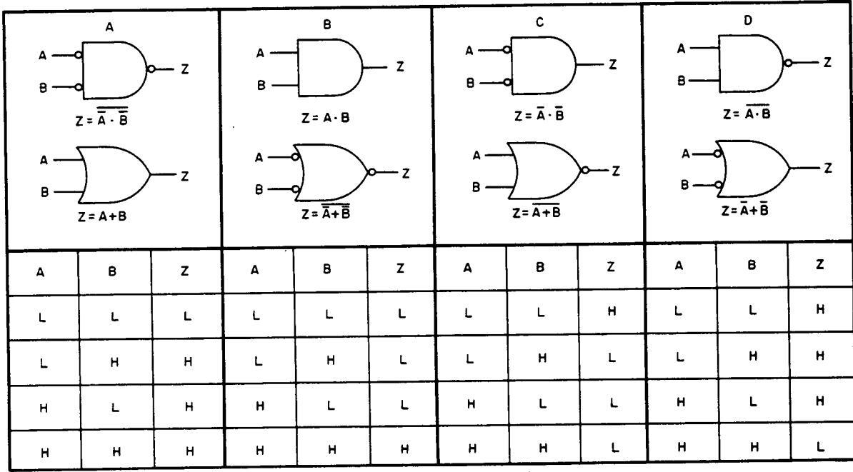
Figure 4-1. Logic Comparison Diagrams
4-5. Logic Levels
4-6. This instrument uses three types of logic. They are:
- 1. Transistor-Transistor Logic (TTL)
- 2. Emitter-Coupled Logic (ECL)
- 3. Emitter-Emitter-Coupled Logic (EECL).
Digital signals have two logic states, referred to as High and Low. The voltage associated with the High or Low state is different for each logic type.
| LOGIC STATE | TTL | ECL | EECL |
|---|---|---|---|
| Low | 0 to +0.4V |
approximately
-1.5V |
approximately
-0.6V |
| High | 2.4 to 5V |
approximately
-0.8V |
approximately
0V |
4-7. Wire-OR/Wire-AND Configuration
4-8. The wire-AND configuration applies to TTL type logic. (It may be commonly referred to as wire-OR.) In TTL, the output of an open-collector gate (one having no load resistor) can be paralleled with gates of the same type to perform this function. When the outputs are tied to the same line, any one of the gates can pull the line Low (.7V) without damaging itself. An external pull-up resistor is required.
4-9. The wire-OR configuration applies to ECL type logic. With ECL, an external resistor is not necessarily required. As with TTL, the gate outputs are connected together. In this case, however, any one of the gates can force the line High (-.7V).
4-10. Exclusive OR Gate
4-11. The output of the exclusive OR will be High if one, but not both, of the inputs is High. This can be seen in the truth table in Figure 4-2.
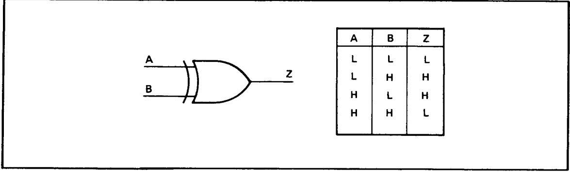
Figure 4-2. Exclusive OR Gate
4-12. INTEGRATED CIRCUITS - THEORY OF OPERATION
4-13. Much of the circuitry used in this instrument is comprised of common logic elements: AND gates, D-Type flip-flops, JK's, etc. Other circuits may use devices that are not as familiar as those mentioned. The following paragraphs briefly describe the operation of these devices. Notice that these devices are shown functionally; i.e., they attempt to best describe the oper-tion of the device and may not reflect the nomenclature used by the manufacturer.
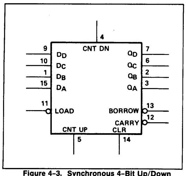
Counter, 1820-0233
4-14. Synchronous 4-Bit Up/Down Counter, 1820-0233
4-15. All four counters are fully programmable; that is, the outputs may be preset to any state by entering the desired data on the data inputs while the LOAD input is Low. The output will change to agree with the data inputs. Once the Load condition is removed, the outputs can count down with each positive pulse on CNT DN or count up with each positive pulse on CNT UP. A High level on the CLR input forces all outputs Low. Borrow goes Low with an underflow condition, while CARRY goes Low with an overflow condition.
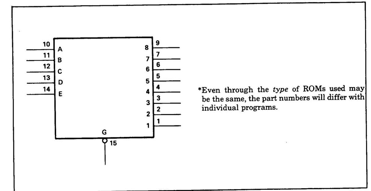
Figure 4-4. Read-Only Memory (ROM) 1820-0254*
4-16. Read-Only Memory (ROM) 1820-0254*
4-17. This device is a programmed, addressable memory. There are 32 storage locations, each of which is capable of storing an 8-bit character. The contents in each location is fixed. The contents of a location are placed on the output lines when the gate (G) is low and the location has been addressed with the proper input code (A,B,C,D,E lines).
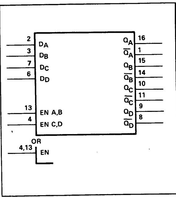
Figure 4-5. 4-Bit Bistable Latch 1820-0301
4-18. 4-Bit Bistable Latch 1820-0301
4-19. Information present at a data (D) input is transferred to the respective Q output when the enable line is High. The Q output will follow the data input as long as the enable line remains High. When the enable line goes Low, the information currently on the D inputs is retained (latched) on the Q output until the enable line returns High.

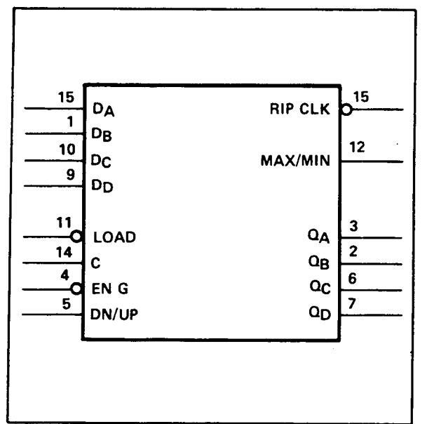
Figure 4-6. Synchronous Up/Down Counter 1820-0545
4-20. Synchronous Up/Down Counter
4-21 A Low on the EN G line enables the operation of this binary counter. While the LOAD input is Low the counter can be preset to any number from 0 to 15. The Q outputs assume this number, and counting begins from that point. The state of DN/UP determines the direction of counting If DN/IIP is High, the counter counts down, when Low, it counts up. The MAX/MIN output produces a High level output pulse with a duration approximately equal to one complete cycle of the clock when the counter overflows or underflows. The RIP CLK output produces a Low-level nulse equal in width to the lowlevel portion of the clock input when an overflow or underflow condition exists.
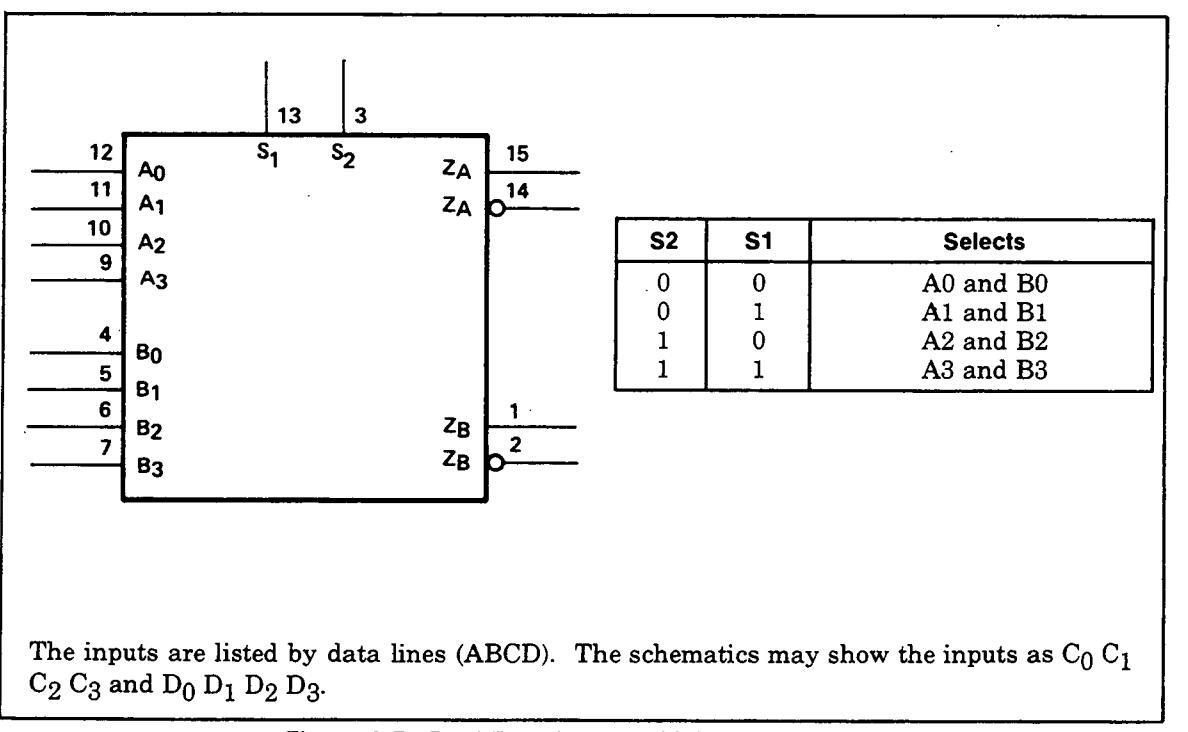
Figure 4-7. Dual Four-Input Multiplexer 1820-0610
4-22. Dual Four-Input Multiplexer 1820-0610
4-23. This multiplexer selects one line from the four A inputs and one line from the four B inputs and transfers that data to the respective Z outputs. Each Z output (A or B) has an inverted and a noninverted line. The inputs to be transferred are selected by the code present on S1 and S2, as shown in the truth table of Figure 4-7.
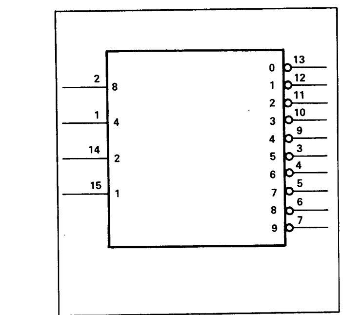
Figure 4-8 One-of-Ten Decoder 1820-0627
4-24. One-of-Ten Decoder 1820-0627
4-25 This IC converts a BCD code to a decimal equivalent. A code on the input lines (8.4.2.1) causes one of the output lines to Low. For example, a code of seven (8421) pulls the "7" line Low
Figure 4-9. MOS Six Decade Counter 1820-0634
4-26. MOS Six Decade Counter 1820-0634
4-27. This is a 6-digit, ripple-through counter with buffer storage outputs for each decade. The circuit has one set of BCD outputs (ABCD) that may be switched from digit to digit, as determined by a decade select code (XYZ). For the counting operation, the device will advance its count on the positive going edge of the clock input (C). While counting is in progress, the decimal count of a selected decade (by means of XYZ lines) is transferred to the BCD outputs when the TRF line is held Low. The decade contents can be "scanned" and transmitted to the BCD outputs by sequentially changing the XYZ code. The High logic level is >3.4V for all inputs.
Figure 4-10. Eight-Input Multiplexer 1820-0658
Figure 4-11. Quad Latch 1820-0701
4-28. Eight-Input Multiplexer 1820-0658
4-29. A Low on the EN line enables the operation of this multiplexer. A code on the select lines (S4, S2, S1) selects the corresponding input to transfer its data to the Z outputs. For example, a code of (S4 S2 S1 / 1) selects the I3 line, and the Z output (noninverted) assumes the state of I3.
4-30. Quad Latch 1820-0701
4-31. Information present at a data (D) input is transferred to the respective Q output when the enable line is Low and when the respective select (S) line is Low. The Q output will follow the data input as long as EN remains Low. When EN goes High the data currently on the D inputs is retained (latched) on the Q output until EN returns Low or the latch is reset (MR=Low). When the latch is reset, the Q outputs go Low.
Figure 4–12. One-of-Sixteen Decoder 1820–0702
4-32. One-of-Sixteen Decoder 1820-0702
4-33. This IC converts a binary code to a decimal equivalent. When the device is enabled with two-low levels (pins 18 and 19), a code on the input lines (8,4,2,1) will pull one of the output lines Low. For example, a code of 12(8421/1102) pulls the "12" line Low.
igure 4-13. Quad Two-Input Multiplexer
Figure 4-14. Synchronous 4-Bit Counter 1820-0716
1820-0833
4-34. Quad Two-Input Multiplexer 1820-0710
4-35. With the enable (EN) line Low, the multiplexer is enabled to transfer the data inputs (ABCD) directly to the output lines (Z). When SEL is a "0" (Low) the A0B0C0D0 inputs are selected; while the A1B1C1D1 inputs are selected with a "1" (High) on the SEL line.
4-36. Synchronous 4-Bit Counter 1820-0716
4-37. The two enable lines (EN P and EN T) must be High before the device can count. Each positive edge of the clock pulse advances the binary count on the Q outputs. The carry output (CO) goes High when the output reaches a count of 15 (a total of 16 clock pulses). The count can be preset to start counting from a given number. This is done by pulling the LOAD line Low and entering the desired number on the input lines (A,B,C,D).
4-38. 8-Bit Addressable Latch 1820-0833
4-39. When the EN line is Low data (D) is written into the latch and will appear on only the Q that is selected by the address code. For example, an address code of 5 (A4 A2 A1 / 0 A1 / 0 Selects Q5. When EN is High, the latch is in the memory mode; i.e., all latches remain in their previous state and are unaffected by the data or address inputs.
Figure 4-16. 5-Bit Comparator 1820-0904
4-40. 5-Bit Comparator 1820-0904
4-41 This IC performs a comparison between two 5-bit characters and provides three outputs to indicate the result of the comparison: less than, greater than, and equal to. A Low level on EN enables the device, and a High level forces all three outputs I ow

Figure 4-17. 64-Bit Read/Write Memory 1820-1028
4-42. 64-Bit Read/Write Memory 1820-1028
4-43. The memory is capable of storing 16 characters of 4-bits each. Information present at the data (D) inputs is written into the memory by addressing (A lines) the desired memory location and holding both memory enable (ME) and write enable (WE) low. The complement of the information that has been written into the memory is read out at the four output (O) lines. This is done by holding ME low, setting WE high, and addressing the desired location.
4-44. OVERALL THEORY OF OPERATION
4-45. The following paragraphs contain a general description of the counter's operation. A block diagram is provided in Section VIII for reference.
4-46. Input Assembly
4-47. The counter has two input channels, each having a frequency range of dc to 500 MHz. A two-position switch selects either X1 or X20 signal attenuation. The signal is amplified by two amplifiers: one on A3 and the other on A4. The sensitivity of the first amplifier is variable with the LEVEL pot. The second amplifier is a combination amplifier/Schmitt trigger. The outputs of the Schmitt triggers drive the gate board.
4-48. Gate
4-49. The main gate board (A9) uses three separate multiplex switches to select the proper signals for a particular measurement. Two of the switches select inputs from Channel A, Channel B, Plug-in A, Plug-in B, and 100 MHz test. These signals are termed event counts, where each pulse represents a count. The third switch selects the internal 500 MHz clock signal, the plug-in clock signal, or the output of the second multiplier for use in the RATIO or START Function. These signals constitute the time counts .
4-50. The main gate board also controls the gating of the input signal and clock signal. The main gate circuits are armed by the run down of sample rate or by the reset signal. The arming signal enables the gate to open on the next input cycle. During the time the main gate is open, the event signal and time signal are divided by 20 in the A9 scalers. The signal levels are shifted from EECL to T2L before the signals are sent to the remainder of the scalers on A11.
4-51. Scalers
4-52. The scalers, or dividers, can be considered as a string of 13, individual, divide-by-10 stages. When the main gate opens, The Event Scaler begins accumulating event counts (e.g., Channel A pulses), and the Time Scaler begins accumulating time counts (e.g., internal 500 MHz pulses). Before the decades can output their data, the accumulation of counts must end with the conclusion of the gate time. A method for determining the end of the gate time is, therefore, needed.
4-53. The GATE TIME switch sends the A11 board a different 4-line code for each of its switch positions. The code is passed through a switch to a strobe coder, where it is decoded to a 16-line code. This code addresses one of the Time Scaler decades to output its data. The Time Scaler accumulates 500 MHz clock pulses until a "5" appears on the output of the addressed decade. Any division of 500 MHz by a power of 10 is also a division of 1 second by the same power. Therefore, when a "5" first appears on the output of the addressed decade, the elapsed time (gate time) is the selected multiple of 1 second. For example, if 5 x 10⁸ counts accumulate in 1 second (500 MHz), 1 ms will accumulate 5 x 10⁵ counts. Once a 5 is detected, the main gate closes on the next Channel A input pulse.
4-54. Each decade of the time and events scalers now contains one digit of information, which can be sent to the processor as a 4-line code. This is done by sequentially addressing each decade to output is stored data. The address codes are supplied to the A11 switch by a 16-bit counter: the Denominator Register Counter (DRC) located on the A13 board.
4-55. Arithmetic Processor
4-56. The data from the time and events scalers on A11 are strobed into the A13 board, where the data is manipulated in such a manner as to double the time data. The Adder/Subtracter circuits perform this operation by adding the time data to itself. This, in effect, produces a 1 GHz time base frequency. This results in keeping the measurement in terms of events/nanosecond.
4-57. Once this is accomplished, the DRC again strobes events data into the A13 board. The events data is now located in the Denominator Register and the doubled time data is located in the Numerator Register. This sequence of events occurs in every frequency, period, or time interval measurement.


4-58. The arithemetic process consists of dividing the contents of the Denominator Register into the contents of the Numerator Register (NR/DR). For mainframe measurements involving a gate time, the process is always a division. The contents of the registers, therefore, may have to be exchanged, depending on the type of measurement being made. For example, in a period measurements, the division needs to be time of the register (1/f) = period); therefore, no exchange is needed, since time data is in NR and events data is in DR. In a frequency measurement, however, the division needs to be time (cycles/sec = frequency); therefore, the registers must exchange their data to perform the correct division.
4-59. Shifting data from one register to another involves "reading" the data out of each register, storing it in a latch, and then "writing" the data back into the other register. Once both groups of data are positioned in their correct register, the Adder/Subtracter Register accomplishes the division by performing a series of successive subtractions . Each time this register completes a successful subtraction, it increments the Quotient Multiplier Counter. Once this counter determines the total number of successful subtractions in a particular digit, it transfers that data into the Quotient Register and continues the subtraction process for the next significant digit. After all subtractions are complete, the Quotient Register shifts the data into the Denominator Register, where it can be distributed to the display or interface bus.
4-60. The Quotient Multiplier Storage circuit is used to determine the unit multiplier (K, M, n, etc.) of the result. The Digit Storage defines the number of significant digits to be computed. The digit counter (DC) is compared with Digit Storage (DS). When DS = DC, the division routine is complete. The Decimal Point Locator for the Result (DPLR) is a counter that keeps track of the decimal point location in the result. The Decimal Point Locator for K is also a counter and is used to keep track of decimal point information from the plug-in.
4-61. State Control Section
4-62. To this point, the counter has been described in terms of signal or data flow. To control the intricacies of the data flow, a hierarchy of commands and controls are needed. Depending on the operating mode being used, the counter uses a particular program which outputs the commands to the various assemblies in the counter. All possible program steps are contained in the ROMs (Read Only Memories), located on A15 (lower left of block diagram). The flow within the program is determined by generating a series of commands and then altering the program flow based on the results.
4-63. The ROMs output two sets of program codes: one set when the MSB address line is High and the other set when MSB is Low. The first set is chosen by address codes, which selects one out of 128 possible ROM address locations. The second set of program codes is chosen from a second set of ROM address locations. Each address location contains a specific program code.
4-64. The first set of program codes is stored in the Word Doubler Storage circuits (A14, A15) until the second set is received. The two sets are then fed to the Combinational Logic circuitry on A15 where the program codes combine to produce about 50 command lines . Some of these command lines come directly from the ROMs. As previously mentioned, the command lines control various assemblies to perform particular functions. The results of the function are carried on lines called qualifier lines . The A10, A11, A13, A14, and A15 boards contain combinational logic circuits which generate the qualifier signals that are sent to the Qualifier Select Logic. The Qualifier Select Logic examines only one qualifier line. The line it examines is determined by the 6-line output of Word Doubler Storage.
4-65. The Word Doubler Storage circuits provide 6 address lines from the previously addressed program codes. These 6 lines contain a two-digit octal code, which performs two functions: (1) it provides the two most significant digits of a 3-digit code, which will be used to address the ROMs to the next address in the program, and (2) it selects the specific qualifier line that the Qualifier Select Logic will output on the LSB (least significant bit) line. The LSB line is the third digit in the 3-digit ROM address code. Therefore, even though there is a definite arrangement of address codes in a particular program, the program flow can be modified by the state of the LSB line, which is the result of the last set of commands.
4-66. Oscillator Circuits
4-67. The internal time base for the counter is supplied by a 10 MHz, oven-controlled oscillator. The 10 MHz signal feeds through a pulse shaper and buffer to J2 on the rear panel and to the plugin circuits. It also feeds into a times 50 multiplier circuit (X2, X5, X5). The result is a 500 MHz signal that is used as the counter's time base. Depending on the state of a status line, the 500 MHz clock may be jittered to provide true time interval averaging. A portion of the signal is transed off after the X10 stage. This 100 MHz signal is used for self-check.
4-68. An external oscillator signal may be applied to J1, EXT FREQ STD INPUT. This signal is sent through a circuit that phase locks the internal oscillator to the external standard.
4-69. Power Supplies
4-70. The power supply circuits are contained on A6 and A7 assemblies. The supplies are short-circuit proof and will automatically shut down if operated at too high a temperature. A sophisticated ground system requires that each supply line be measured to its own return line, e.g., +5V and +5V RET (return).
4-71. CIRCUIT BOARD THEORY
4-72. The following paragraphs describe the operation of each circuit board in the counter. Refer to the appropriate schematic in Section VIII while reading this material. If the reader's purpose is to learn the instrument's operation, rather than a specific part of the counter, it may be helpful to read the material in the suggested order: A3, A4, A9, A11, A10, A13, A15, A14, A1, and A2
4-73. A1 and A2 Display Assemblies
4-74. Assemblies A1 and A2 combine the circuits necessary to display all measurement data, minus sign, and annunciators. The A1 board contains the digit LEDs, which are placed in sockets, and the annunciators, which are backlighted by incandescent lamps. A2 contains the character generator and its drivers, the decimal point decoder, and the digit enable circuit with its drivers. The annunciator decoding is shared between the two boards.
4-75. STROBING TECHNIQUE. The result of the measurement is displayed by using a strobing technique. That is, only one digit of the displayed number is on at any one time. One digit is displayed and then removed; then the next digit is displayed and removed. This process continues until all digits have been shown. The strobing process occurs at a faster rate than the eye can detect, so the display appears continuously lit. Character generator A2U6 controls the digit (numeric character) to be displayed, while A2U1 controls the placement of the digit in the display.
4-76. CHARACTER GENERATION. The BCD data lines (entitled DR A,B,C,D) carry the digit information from the DR RAM (A13) to the character generator, A2U6. The BCD lines are decoded by A2U6 into segment lines for the LEDs. Each segment line enables an individual segment (or diode) of the LED display; therefore, several of these output lines may be High when displaying a specific digit. Transistors A2Q1 through A2Q7 are used as drivers for the segment lines. A2Q8 drives the decimal point line (described later).
4-77. Since these lines connect to the same segment in each digit, the turn-on of these digits must also be controlled. The same counter codes that address the data from the DR RAM are also sent to A2U1. They are then decoded to turn on each digit, in sequence, from LSB to MSB. Eleven codes are needed to display all possible digits; therefore, the DRC codes are normally stepped from 0 to 10.
4-78. As the DR counter steps through its codes, the data lines (DR) and DRC lines change codes and each digit is displayed. The counter steps through all 11 codes, regardless of the number of digits displayed. A DR code of 15 will blank those columns that have no digits. If the measurement requires a minus sign, the DRC lines provide an additional code of 11. This causes A2U1(13) to go Low. This results in A2Q9 driving the anode of A1DS1 and, at the same time, enables A2U4B and A2Q7 to drive the cathode.
A1 and A2 Continued
4-79. When the LAMP TEST line goes Low, it forces all outputs of A2U1 to go High, which lights all segments of the display. This line also enables A2U4A to light the decimal points. During lamp test, the DRC lines step through all 16 codes (0-15).
4-80. ENABLE CIRCUITS FOR CHARACTER GENERATION. Before A2U1 can operate, both G1 and G2 inputs must be Low. Likewise, the RBO line of A2U6 must be High before the device can drive the segments. During the process cycle, the DISP CLK EN line is Low. This resets A2U7A and places a High on the G2 input of A2U1, thereby turning it off. When the display cycle begins, DISP CLK EN goes High and releases the rest position, Also, the DRC code returns to zero. This causes a High-to-Low transition on the DRC D line, which clocks A2U7A, a retriggerable one-shot multivibrator. The "time-out" for this one-shot is longer than the time required to strobe the display. If, for some reason, the DRC codes become inactive, the one-shot will time-out and turn off A2U1 by placing a High on G2.
4-81. A new digit is clock out of the DR RAM with each negative transition of DISP CLK. When this line goes Low, however, it triggers A2U7B, a one-shot multivibrator. This produces a High on the Q output to turn off A2U1 via the G1 line. It also produces a Low on the Q output, which blanks A2U6 and forces its output lines Low. This same pulse also shuts off the decimal point by placing a Low on A2U3(3). The duration of these pulses is controlled by R26 and is in the order of about 5 to 50 µs. This provides enough time for the RAM circuits to settle after selecting another digit. Once the one-shot times out, the Q output of A2U7B returns Low to enable A2U1 and the Q output returns High to enable A2U6.
4-82. DECIMAL POINT GENERATION. As previously stated, each DRC code represents a specific position in the display. This is also true of the decimal point code, which is transferred on the DP A,B,C,D lines. The position of the decimal point in the display has been determined in the process cycle. The code is placed on the DP lines for the duration of the display cycle. These lines are connected to one side of four exclusive OR gates (A2U2), while the other side of these gates is connected to the DRC lines. When the two codes are equal, all inputs to A2U3B go Low. This enables A2U3A and A2U4A to turn on A2Q8 and light the decimal point.
4-83. ANNUNCIATOR CIRCUITS. The multipliers for the measurement (M, K, µ, etc.) are generated by a decoding network, comprised of A2U5A,B, and C, A1U2A and B, and A1U1. Since this counter can make period measurements, in, say, kiloseconds or frequency measurements in terms of Micro Hertz, the decoding circuits must meet these criteria. Because A1U1 is an open-collector 4 to 10 line decoder, its outputs can be wired together or to additional circuitry. A table is provided with the schematic to explain the functional decoding of this circuit. The other annunciators are driven directly or through individual buffers. NAND gate A2U4D ensures that the ARM light is on only when the GATE light is off.
4-84. A3 Input Amplifier
4-85. The Input Amplifier consists of two similar input channels, Channel A and Channel B. The channels are completely separate, and can be selected for common or separate operation. Each channel has ac or dc coupling, selectable 50Ω or 1 MΩ impedance, an attenuator network, level control, preset control, slope selection, and a high-frequency Schmitt Trigger Amplifier.
4-86. CHANNEL A. The circuit theory describes only the Channel A circuit, since the Channel B circuit is similar. The signal entering input connector J3 is sent directly through switch S8 or through coupling capacitor C22, which blocks the signal's dc component. Switch S5 selects SEP or COM mode of operation. Switch S6 selects resistor R25 for 50Ω input impedance and resistors R28 and R27 for 1 MΩ input impedance. When S5 is in the COM position and S6 is set to 50Ωs, the two channels are connected together and resistor R26 maintains the 50Ω input for each channel. In SEP, the inputs are isolated from each other, R26 is bypassed, and the impedance switches can be set separately. Attenuator Switch S7 passes the signal directly in divide-by-1 or attenuates the signal by 10, in divide-by-10, through divider network R28 and R27.
4-87. The conditioned signal is then routed to the Schmitt Trigger Amplifier U2(8) through one of two paths, depending on the frequency. Frequencies below 10 MHz including dc, pass through the source follower FET Q3A. Higher frequencies are bypassed around the FET through capacitor C24. Q3A input is protected at low frequencies by resistor R36, and diodes CR5 and CR6. The amplifier U2 has differential inputs and outputs (only one output line is used) and has a gain of about 3. One input accepts the signal and the other accepts the dc level (-2V to +2V) from the front panel LEVEL/PRESET (pot/switch), or remotely via HP-IB (Option 012). Sensitivity potentiometer R41 enables optimum sensitivity adjustment of Amplifier/Schmitt Trigger U2. Adjusting R41 varies the voltage at the gate of source follower Q3B, thus varying the voltage at Pin 7 (TRIG) of U2. Adjusting R41 also varies the voltage at connector J2(2). FETs Q4A/B are current sources for Q3A/B.
4-88. Manual control of trigger level voltage is accomplished by adjusting LEVEL/PRESET control pot/switch (R38). The trigger level can be PRESET to zero volts, or varied from -2 volts to +2 volts. For Remote control via HP-IB, the trigger LEVEL pot must be set at PRESET (0V) position.
4-89. The counter may be triggered on either slope of the input signal. The SLOPE switch S9 determines this by controlling the output polarity of U2. If S9 is placed to +, a dc voltage of 3.5 volts is present at U2(6) (SLOPE) which enables U2 to trigger on the positive slope of the input signal at U2(8). If placed to -, 0 volts is present at U2(6), and U2 will trigger on the negative slope of the input signal.
4-90. A4 Input Trigger Assembly
4-91. A4 Input Trigger Assembly directly connects the amplified Channel A and Channel B signals from the A3 assembly to the A9 Main Gate assembly. The A4 assembly also provides adjustments for the hysteresis and risetime of A3U1 and U2 outputs, and controls clamp voltages for the input protection diodes on the A3 assembly.
4-92. CHANNEL A. The following circuit theory describes only Channel A, since Channel B is identical. The amplified Channel A signal from A3U2(1) enters at A3P2(6) and goes straight through to the A9 Main Gate assembly via connector P3(2). Analog Adder A4U1 senses the dc trigger level from A3J2(2) and outputs a corresponding set of dc clamp voltages to the input protection diodes A3CR9 and CR10. With a nominal trigger level of 0V at A3U1(3,5), the output is -2V at U1(1) and +2V at U1(7). When the trigger level changes, each output is offset by an amount equal to that change. For example, if the trigger level is +1V, the output at U1(1) is -1V (-2V plus +1V) and the output at U1(7) is +3V (+2V plus +1V).
4-93. A5 Front Panel Interconnect
4-94. This assembly provides an interconnection between the A4 Input Trigger Assembly and the A16 Motherboard Assembly. It also contains two coax cables for transferring the Channel A and Channel B signals to the A9 Main Gate Assembly.
4-95. A6 Switching Regulator
4-96. The A6 assembly provides +5V Display, +5V, and -5.2V for distribution throughout the instrument.
4-97. +5V DISPLAY SUPPLY. Rectifier diodes CR1 and CR2 receive 17V rms from the secondary of T1. C3 filters the resultant 8 Vdc. When the POWER switch is ON, P1B(7) is at ground potential. This causes CR4 to conduct and turn on Q2, which places 8V on U3's input. CR6 also conducts through R5, causing Q3 to turn off. U3 regulates the output voltage at +5V and provides fold back current protection. C7, C11, and C13 filter ac signals from U3. If the POWER switch is set to STANDBY or should S1 open, CR4 no longer conducts and Q2 turns off U3. With CR6 also turned off, Q3 is allowed to turn on through R5. This places a 100Ω load on the 8V unregulated line, which helps keep the high line peak voltage within the voltage rating of C3.
A6 Continued
4-98. THERMAL AND ELECTRONIC SHUTDOWN. S1 is a thermal switch that is mounted on U2. P1B(7) connects to the POWER switch and is at ground potential with the switch set to ON. When S1 is closed, there is .7V on the base of Q1, because of CR3. If the switch opens, due to high heat sink temperature, CR3 no longer conducts. This allows Q1 to turn on. Q1's collector voltage drops to a few. tenths of a volt, which allows base current to flow in both Q5 and Q6 and causes them to turn on. Q6 turns on Q8. Q5 and Q8 turn on transistors inside U2 and U1, respectively, which turn off their internal current sources and shut off the two regulators. S1 shuts off the +5V DISPLAY supply by turning off CR4 and Q2. These three supplies are also turned off if the POWER switch is placed in STANDBY.
4-99. +5V REG SUPPLY. The +5V REG and -5.2V REG supplies receive power from the 22.3V rms secondary of T1. F1 and F2 provide protection for the rectifier circuits, while C1 and C2 prevent internally generated EMI from entering the power cord. CR5 rectifies the ac into +14 Vdc and -14 Vdc supplies. The voltages are filtered by C4-C6. U2 is connected as a switching type voltage regulator, whose output of +5V varies about 30 mV plus and minus at about 18 kHz. Output current is supplied through Q9 current boost.
4-100. When U2 turns on, it draws current through R25. This produces a voltage drop across R25 and turns on Q9. The output of Q9 charges L1 and C16 and increases the voltage on the output. When the output voltage reaches about 30 mV above +5V, it is sensed at U2(5), via the short on the motherboard. U2 shuts off current through R25, thereby shutting off Q9. The field around L1 collapses and causes "catching" diode CR10 to conduct. C16 also discharges until the output voltage drops to about 30 mV below +5V. This voltage is again sensed at U2(5) and Q9 is again turned on. The values of L1 and C16 help determine the switching rate. Q11 limits the output current of U2 during Q9 turn on or should Q9 fail and the regulator attempts to output more current than it is capable of delivering. CR8 and CR9 serve as clamping diodes and prevent the internal circuits of U2 from saturating and causing a slower switching rate.
4-101. Bi-directional Crowbar. Should the output voltage become excessive due to a failure in the supply (e.g., Q9 shorted), the crowbar prevents damage to the counter by shorting the output line to common. This is done when the output voltage reaches +6.3V or is shorted to a negative voltage. In either case, CR16 and CR17 conduct and trigger triac CR14. This will probably cause F3 to open.
4-102. Sense Line Clamp. The power supply boards should not be removed with the power cord connected. If this occurs, the sense line is disconnected from the +5V output (short on motherboard). Even though the board is removed, power is supplied by the filter capacitors, C4 and C6; and the internal voltage tends to approach +14V, possibly causing damage. To prevent this, diode CR10 conducts and resembles the motherboard short. This regulates the supply at about +5.7V until the stored voltage bleeds off.
4-103. Current Limit. Q4 and Q7 form an equivalent SCR. If the output draws too much current (=6A), the current sense resistor R7 developes a voltage drop sufficient to turn on Q4. Q4 turns on Q7, which causes Q4 to turn on even harder. The result is that the internal circuits of U2 are deprived of current and shut down the output of U2. Should Q5 turn on (POWER switch to STANDBY or S1 open), it causes the current to flow through Q5 instead of Q4 and Q7. Once this occurs, Q4 and Q7 can be considered "unlatched."
4-104. -5.2V REG SUPPLY. This supply is similar in operation to the +5V REG supply. The only differences being that R32 substitutes for Q11 and R34 as a peak current limiter, and CR7 substitutes for Q4 and Q7. As with the other supply, too much current through R12 triggers the SCR. This places -14V on CR7's anode, which draws current out of U2. The result is that U4's output and Q10 turn off. Should Q6 turn on (POWER switch to STANDBY or S1 open), it causes current to flow through Q8 instead of CR7. When the anode current of CR7 goes below its holding current (=5 mA), the SCR unlatches. When Q8 turns off again, the time constant of C10 and R21, 22, and 24 slows the dv on CR7. This prevents the SCR from turning on with a sudden change in anode voltage.
4-105. A7 Linear Regulator
4-106. The A7 assembly provides +12V, +15V, and -15V for distribution throughout the instrument
4-107. +12V OSCILLATOR SUPPLY. The 12V, 22V, and 11V supplies receive power from the 36V rms secondary of T1. F1 and F2 protect the rectifier circuits, while C1 and C2 prevent internally generated EMI from entering the power cord. CR2 rectifies the ac into +22 Vdc and -22 Vdc supplies. The voltages are filtered by C6-C9, while R6 and R7 serve as bleeder resistors. The +22V unregulated supply is sent out on P1A(10).
4-108. U2 is the 15V regulator whose output is filtered by C18 and C21. R21 and CR8 step the voltage down to +11V regulated and C14 filters the output.
4-109. Regulator U2 uses foldback current limiting and is thermal protected. Should the 12V output short to common, the voltage drops to zero and the current "folds back" to a safe value of current. If, in addition, the IC's temperature increases, the output shuts down completely, turning on again once the chip has cooled down. These actions prevent the supply from short-circuit damage. The +22V supply continues to supply power to the oscillator circuits with the POWER switch set to STANDBY or when the other supplies have shut down due to high temperature.
4-110. THERMAL AND ELECTRONIC SHUTDOWN. S1 is a thermal switch that is mounted on U4. P1B(6) connects to the POWER switch and is at ground potential with the switch set to ON. When S1 is closed, there is .7V on the base of Q3, because of CR3. If the switch opens, due to the high heat sink temperature, CR3 no longer conducts. This allow Q3 to turn on. Q3's collector voltage drops to a few tenths of a volt, which allows base current to flow in Q4 and causes it to turn on. Q4 and CR6 turn on transistors inside U1 and U4, respectively, which turn off their internal current sources and shuts off the two regulators. S1 shuts off the +20V REG supply by turning off Q2. These three supplies are also turned off if the POWER switch is placed in STANDBY.
4-111. +15V SUPPLY. The +22V line supplies input voltage to U1 pin 3. The +15 regulated output voltage is present at P1A(8,8), via Q5 and R28. The motherboard sends this voltage back to P1A(7), where it is sent to U1(5) as the sense voltage.
4-112. Any voltage change on the sense line is compensated for by a subsequent change in output current in a direction necessary to counteract the change in output voltage. Since the regulated output of U1 is unable to supply high current to the +15V load, it is used as base drive for Q5 current boost. As the load increases, the base current increases, and Q5 draws more load current from the +22V supply. Should the load draw too much current, as in the case of a short, Q7 (normally off) conducts via R22. The collector of Q7 sinks current from the internal circuits in U1 that would normally drive Q5. Depriving Q5 of base current drops the output current to some nominal value, hence, foldback.
4-113. Sense Line Clamp. The power supply boards should not be removed with the power cord connected. If this occurs, the sense line is disconnected from the +15V output (short on mother-board). Even though the board is removed, power is supplied by the filter capacitors, C6 and C8; and the internal voltage tends to approach +22V, possibly causing damage. To prevent this, diode CR12 conducts and resembles the motherboard short. This regulates the supply at +15.7V until the stored voltage bleeds off.
4-114. -15V SUPPLY. The -15V supply is similar to the +15V supply; therefore, only the differences will be described. CR6 is used as the shutdown control for U4. With shutdown, U4's output turns off Q6.
4-115. +20V REG SUPPLY. Diode assembly CR1 rectifies the 22V rms voltage into 28 Vdc, which is filtered by C4. U3 is a +15V regulator whose common side is held at +5V. The result is a regulated +20V output. CR10 clamps the common terminal to the output in the event of a short to common. This prevents reverse biasing of circuits internal to U3, preventing damage to the IC.
4-116. A8 PLL Multiplier Noise Generator
4-117. The A8 assembly performs several processes, all of which pertain to the oscillator signal. The main function is to accept the internal 10 MHz oscillator signal and from it produce the 500 MHz time base signal. Other signals derived from the 10 MHz input are the 100 MHz test signal, used for the Check Mode; an amplified 10 MHz signal for the rear panel; and another amplified 10 MHz signal for the plug-in accessories. Another function of the board is to phase lock the internal oscillator signal to an external reference. At appropriate times, the board also places white noise on the time base signal, thereby preventing a harmonic relationship between the time base signal and input signal.
4-118. INPUT AND MULTIPLIER CIRCUITS. The 10 MHz oscillator signal enters differential amplifier U3, which serves as an isolation amplifier. This stage prevents changing load currents from affecting the oscillator, itself. One output of the amplifier, pin 6 (TP1), is decoupled by C15 and sets the bias of Q4, 5, and 6 at 8.5 to 9 Vdc. These three transistors form one side of a differential amplifier, while the other side, Q7, accepts the output signal from U3 pin 8 (TP2).
4-119. Output Amplifiers. The output of U3 is transferred from the emitter of Q7 to the emitters of the other three transistors, which constitutes a common base configuration for these stages. There are four outputs from these stages. Q7 provides 10 MHz to the rear panel through an impedance matching network, comprised of L7, C30, and C31 (TP5). Zener diode CR14 prevents the output signal from reaching too high of a level when J2 is not loaded with 50 ohms. Another stage, Q6, sends 10 MHz to the plug-in through a similar circuit, consisting of CR15, L8, and C32 (TP6). The remaining two signals are sent to the phase detector circuit and the multiplier circuits.
4-120. Multiplier Circuits. The 10 MHz signal from Q5 feeds into a tank circuit, consisting of L9-11, C24, C26, C29, and CR12. This circuit presents two signals, 180 degrees out of phase, to the bases of Q8 and Q9. The transistors form a full-wave rectifier circuit and have the effect of doubling the frequency, while providing current gain. The resultant 20 MHz signal (TP14) is smoothed by L12 and C39, before being amplified in U5. The output signal at U5(6) feeds into the tank circuit of C42, C43, and L13. It is then fed through coupling capacitor C46 (TP15) and into the X5 multiplier of U6B, C50, C52, and L14. The multiplier output is a current square wave, which are high in odd harmonics. Tuning capacitor C52 sets the tank circuit to select the 5th harmonic of the fundamental. The resultant 100 MHz output (TP16) is amplified and filtered by U6A, C56, C57, and L15. The gain of this stage can be varied by R81 (RA). Emitter follower Q17 sends the 100 MHz signal (TP17) off the board for use as a test signal during the check mode.
4-121. The collector of Q17 passes the signal to a phase shifter circuit, comprised of L17, L18, and C68. Adjusting C68 varies the phase relationship between the 100 MHz signal and the 500 MHz signal. The 100 MHz signal can be shifted ±36°, which is 360° with respect to 500 MHz (72° x 5 = 360°). This means a full period of adjustment for synchronization between the two signals. When in the Check Mode, the adjustment eliminates the ±2 ns error incurred in a time internal measurement.
4-122. The 100 MHz signal is amplified by U7B, which uses L19 as a load. The signal passes through coupling capacitor C74, before being further amplified in U7A. The gain of U7A is controlled by R99 (RB). The last stage switches current between output transistors and produces square waves of current, which are high in odd harmonics. A quarter wave length transmission line (etched on board) and C67 (CF) tune the 500 MHz output signal (TP18). Further filtering is provided by C65, L16, C60, and C61. The final stages of amplification are provided by Q19 and Q21.
4-123. During totalize, Channel C events, or a ratio measurement, A8 turns off the 500 MHz time base signal. When the 500 MHz OFF line goes low (-2V from +2V), it turns on CR19 and CR20. The diodes sink collector current from Q18 and Q20. This turns off Q19 and Q21, since they no longer receive any base current.
4-124. NOISE GENERATOR. No noise is generated when the NOISE CONTROL line is High. At this time, both Q1 and Q2 are turned on. The collector of Q2 places -15V on the cathodes of CR5 and CR6, which results in biasing U8 and U9 out of their operating range.
4-125. Once the NOISE CONTROL line goes Low, it turns on CR1 and places the emitter of Q1 at about 0.7V. This turns off Q1 and Q2 and turns on U9 and U8. The noise generated from Zener diode CR2 is amplified by U9. The noise signal couples to U8 through C12 and C11 and is amplified by U8. The cathode of peak detector CR7 sits at about 2V. The noise, therefore, must be at least -2.7V for the diode to conduct. Any noise greater than this passes through the diode and is filtered into an average dc voltage by C20 (TP12). The higher the noise, the more negative this voltage becomes. An increase of negative voltage tends to turn off Q3, thereby increasing its drain resistance. This results in more of U9's output signal being fed back to its inverting input (pin 2) and causes a corresponding drop in output voltage. The output of U8, then, is constant, due to automatic gain control.
4-126. The output noise of U8 passes through R23, C21, and R41 to the cathode of the voltage variable capacitor, CR12. This capacitor is part of a 10 MHz tank circuit, comprised of C24, C26, C29, and L9-11. As the erratic changes in noise voltage affect CR12's capacitance, the phase of the 10 MHz signal shifts rapidly. The result is a 500 MHz time base signal that is phase modulated so rapidly and erratically that it cannot be harmonically related to any input signal.
4-127. PHASE LOCK LOOP. An external signal applied to the rear panel jack enters the board on J1. Limiting diodes CR3 and CR4 prevent excessive voltages from damaging the input circuits. The first two inverters, U2B and U2A, form a feedback trigger circuit and prevent noise from entering the circuits when no input is present. The output of U2A also feeds U2C and a delay circuit, formed by R21 and C17. The time difference between these two signals produces a positive voltage spike on U2D(15) and a negative voltage spike on U2D(9). These pulses are amplified and inverted in U1.
4-128. The phase detector circuit conducts during the time these pulses are present. During conduction, the circuit passes a small segment of the internal 10 MHz oscillator signal, which charges C33 to the value sampled. Each subsequent sample either adds to the previous charge or subtracts from it. A composite picture of many samples appears as a sine wave of the difference frequency.
4-129. When the difference frequency is too high or when the circuit is phase locked, the ac signal at TP10 is zero. At this time, Q14 and Q15 are turned on and force Q16 off. This places a High on the LAMP TEST line. The current drawn through Q14 turns on Q11, which results in shutting off Q10.
4-130. When the signal at TP10 is at a frequency that can be locked and the circuits are attempting to lock, the signal's amplitude is sufficient to drive the unlocked detector, Q12 and Q13. Diodes CR17 and CR18 pass only the positive going portions of the signal. C81 charges to a more positive level than before, which causes Q14 to turn off. Since no collector current is present, Q15 turns off, allowing Q16 to turn on and pull the LAMP TEST line Low. The gate of Q10 becomes more positive, since Q11 is also off, and allows the FET to pass the signal to the VCO on A18. Using this signal, the internal oscillator adjusts itself until it locks to the external standard.
4-131. Once the circuit locks, it opens FET Q10 and adds low pass filter R55, C45, C49, and R74 to the VCO signal line (TP11). This reduces any noise on the external standard line, connected to the back of the counter, and prevents miscounting. Rear panel switch S9 (FREQUENCY STANDARD INT-EXT) controls whether an external signal applied to the rear panel EXT FREQ STD input is used to control the counter. Q22 prevents the counter from operating off of the internal oscillator when in the EXT STD mode and the external frequency is lost or disconnected. When S9 is set to EXT, a ground is connected to Q22 emitter to enable a detector circuit composed of Q22, C84, CR21, and CR22. As long as the external frequency is present at U2D(15), Q22 is shut off. Loss of the external standard causes Q22 to conduct and initiate a front panel LAMP TEST display.
4-132. A9 Main Gate
4-133. This assembly contains 3 primary blocks: Input Selector, Main Gate, and Scaler. All input signals and reference signals (time base) are presented to the Input Selector circuits, which select only those signals needed to complete a given measurement. The Main Gate circuitry determines the precise moment these signals are passed to the scalers and, in addition, sets the


A9 Continued
timing requirements for a time interval measurement. The scalers count the input pulses of both the input signal (events) and reference signal (time) and, at the end of the gate time, outputs the stored data. Subsequent scalers are located on All. A fourth block, Turn-off Control, controls the existence of the 500 MHz internal time base signal, as well as the Channel A and Channel B signals.
4-134. FREQUENCY OR PERIOD MEASUREMENT. Assume a frequency measurement is being made from the front panel. (A period measurement is analogous.) The control lines (see Table 4-1) determine the signal path through the Input Selector circuits. With a Low on U14(11 and 12), the MF CH A signal is allowed to pass through U14D and A. If a signal is also connected to CHANNEL B jack, it will pass through the Channel B Multiplexer U15, but will be blocked by U12A and B (pins 6 and 14 are High). The disabled U6A (pin 8 = H) places a Low on U11(11), which enables U11C to pass the input signal to U5(13) and U10(15). At the same time, the Channel C Multiplexer U13 passes the 500 MHz clock signal to the clock input of the Time Gate F-F, U7(13). Now that both signals are present on their respective flip-flops, a set of conditions must be considered. Both gate flip-flops have been set (Q=H) by the GATE RST signal. U7(3) is High from the High outputs of U5(6) and U6B. The disabled U6A has set U5(1) Low, via U1B. The High outputs of U5 and U7 flip-flops prevent U4 and U2 from toggling. The TI+EVT line is Low and allows U10 to pass the input signal to the disabled U4(13).
| Control Lines (EECL) | |||||
|---|---|---|---|---|---|
| Selected input Signal | Test | Ext AB | Ext C | ||
|
100 MHz TEST
MF CH A AND CH B PI CH A AND CH B 500 MHz CLK PI CH C |
H
L L X X X |
X
L H X X |
X
X X L H |
||
| Control Lines (EECL) | |||||
| Ratio + S1 | г ті | + EVT (P1B pin 14) | |||
|
FREQ OR PERIOD
RATIO OR START/STOP TI OR EVENTS |
L
H L |
L
L H |
|||
Table 4-1. A9 Control Lines
4-135. Noting the timing diagram of Figure 4-18, it is seen that once the GATE ARM line goes High (ECL), it places a Low (EECL) on U5(3). This allows the next input signal to toggle the Event Gate flip-flop. This does two things. (1) It places a Low on U4(14), which enables U4 and allows the next input pulse to enter the Event Scaler. (U4 is a binary of the scaler). (2) It places a Low on the D input of U7, which allows the next 500 MHz clock pulse to toggle the flip-flop and and enable U2 with a Low on C1. This allows the clock signal to enter the Time Scaler. Binaries U4 and U2 pass their divided (÷2) signals to U9 and U3, respectively, where the signals are further divided-by-10. The divide-by-20 input and clock signals are sent to the A11 Scaler board through emitter followers Q15-18.
4-136. The GATE ARM line goes Low once the total number of counts in the time scaler exceeds Gate Time. U5(6) goes High on next input pulse after GATE ARM goes Low. This disables U4 and shuts off the Event Scaler. On the next clock pulse after U7(3) goes High, U2 is disabled by a High on C1, which shuts off the Timer Scaler. Note that only integral (whole) periods are counted in the Event and Time Scalers. This is not true, however, in the totalize (start/stop) mode.
4-137. TOTALIZE MODE. The counter will totalize Channel A pulses for as long as the FUNCTION switch remains in the START position. In this position, the RATIO + ST line is High and causes Q2's collector to go High. This enables U13B and disables U13D from passing the 500 MHz clock signal. The Low on Q1's collector enables U12B to pass the Channel B signal (totalize can be A+B or A-B). The signal passes through U13B to the Time Gate F-F, while the Channel A signal follows the same path that it would in a frequency measurement. The GATE ARM signal is always High in totalize.
4-138. The measurement ends when the FUNCTION switch is placed to STOP. This causes the GATE RST line to go High and set the Event Gate and Time Gate flip-flops. Integral periods are not counted, since the measurement can be interrupted at any time.
Figure 4-18. A9 Timing Diagram for Frequency, Period, Ratio, and Start/Stop
4-139. RATIO MODE. The Ratio mode uses the same signal paths as the Totalize mode. That is, Channel A signal is sent to the Event Scaler and Channel B signal is sent to the Time Scaler. Unlike totalize, the Ratio measurement cycle is based on a selected gate time; therefore, it is dependent on GATE ARM. Since the Channel B signal is a direct replacement of the 500 MHz clock, the lower the frequency of Channel B, the longer the measurement time (see Section III).
4-140. TIME INTERVAL MODE. In this mode, the Time Scaler will count 500 MHz clock pulses only during the time between a Channel A pulse and a Channel B pulse. The two input channels regulate the switching of the clock signal by controlling the Event Gate F-F and Time Gate F-F. Refer to Figure 4-19.
4-141. The High on TI+EVT line causes U4(13) to stay Low, thereby enabling the binary to respond to the output of U5, only. Since U5 and U7 have been set (Q=H) by a High GATE RST, U6A is disabled, which results in a Low on U5(1) and causes U11C to be enabled. The first Channel A pulse to arrive after the GATE ARM line goes High clocks U5 and causes its output to go Low. This causes the output of U7 to go Low with the next clock pulse and enables U2 to pass 500 MHz clock pulses to the Time Scaler. The output of U5 also changes the output states of U6A, causing a High at U5(1) and allowing U11B to pass the next incoming Channel B pulse.
4-142. The Channel B pulse clocks the High on U5(1) onto the QA output. This clocks the C2 input of U4 to register that one time interval has occurred. On the next 500 MHz clock pulse, the High on U7(3) is clocked onto U2(13) and disables U2 from registering any more clock pulses.
4-143. TURN-OFF CONTROL LOGIC. To prevent possible cross talk of high frequency signals under certain conditions, it is necessary to turn off some of the unused internal signals. For example, the internal 500 MHz clock is turned off when using the external clock from the plug-in or when performing a ratio measurement.
Figure 4-19. A9 Timing Diagram for Time Interval
4-144. When the RATIO + ST line goes High, it turns on Q1 and turns off Q2. The High on Q2's collector turns on Q4, causing its collector to go Low. Q9, CR2, and R43 form an emitter follower, which level shifts the Low on the collector of Q4 to -2V on the 500 MHz control line. The Control line turns off the internal clock (+2V=ON). The same thing applies if the EXT C line goes High.
4-145. If the plug-in Channel A and Channel B signals are being used, the EXT AB line goes High and shuts off the mainframe's input triggers. The High on EXT AB turns on Q3, which saturates Q8 and Q10 and pulls the trigger line High. This turns off the Schmitt triggers on A4. R50 and R51 form a 10-to-1 divider network with two resistors on A4 (A4R22 and 24).
NOTE
Simplified flow diagrams for A9 are given in Figures 5-14 through 5-16.
4-146. A10 Gate Control
4-147. The A10 board is closely related in operation with the A9 Main Gate board. The board controls the various methods of arming the counter. Each of these methods must set the Arm F-F, which remains set throughout the measurement phase. The Resolution circuit detects a 5 code from the scalers and signals the end of the measurement. The board provides signals necessary to terminate the measurement, start the processing cycle, and reset the scalers. The function codes (front panel, remote, or plug-in) are decoded through switching and combinational gating and are sent out as control signals. These lines instruct the counter to perform unique functions for the selected mode.
4-148. CONVENTIONAL ARMING. The sequence of events for a frequency measurement, for example, would be sample rate arm, measure, process, display, and back to sample rate arm. At the end of the processing cycle, the sample rate circuit begins its rundown as the previously taken measurement is being displayed.
Figure 4-20. Measurement Timing Diagram
4-149. At the end of sample rate, the ARM line goes Low and sets the Arm F-F, U18A and B. If the rear panel GATE CONTROL switch is set to INTERNAL, the resultant ARMED signal turns on U17C, which enables the Event Gate F-F on A9. The complement signal, ARMED, passes through translator U20B and turns on the ARM light on A2. The next Channel A pulse sets the Event Gate F-F (A9) and drives the EVT GATE line low, which turns on the GATE light and turns off the ARM light. The ARMED line also places a High on the cathode of CR1, located in the Resolution circuit. Once the time scaler outputs a 5 code, a High is placed on each cathode of diodes CR1-4. This places a High on the J input of U22A and toggles the Q output High. The ECL High on U11B(4) and the ECL Low on U11C(9) reset the Arm F-F. The cathode of CR1 goes Low again, thereby preventing a 5 from toggling the Resolution F-F during the process phase when data is being read from the scalers. The reset state of the Arm F-F permits the Event Gate F-F on A9 to terminate the measurement on the next Channel A pulse. This is done when the disabled U17C forces the GATE ARM lines to their "false" states.
4-150. MAIN GATE STATUS. After arming, the first Channel A pulse sets the EVT GATE line Low, which causes U22B to set. The MEAS TIME line goes High and enables the Excessive Gate Time F-F on A11. Two nanoseconds later, the TIME GATE line goes Low, but has no effect on the MEAS TIME output until after a 5 code is detected and the Arm F-F resets. The Arm F-F resets U22B. At this time, the TIME GATE line holds the ECL wired-OR High, through U23C and U21C and D, until it also goes Low one time pulse after the Event Gate F-F resets.
4-151. During slow gate times, the GATE light is on for as long as the wired-OR line is High. With fast gate times, a 40 ms one-shot ensures that the GATE light is visible by keeping the GATE LITE line Low for 40 ms after the main gate closes.
4-152. INITIALIZE PROCESSOR CIRCUIT. The processing cycle begins when the measurement cycle is complete and the main gate closes. When the MEAS TIME line goes Low, it allows U12A to clock the Measurement Done F-F, U12B. The Q output goes Low and allows U13B and C to pull the INIT PROC line Low, thereby starting the process cycle. At near completion of the process cycle, the RST FRONT END line goes High and resets U12B via U10F and E.
4-153. ARMING AND PROCESSING IN TOTALIZE. During a totalize measurement, the process cycle is not controlled by the main gate. There is no gate time in an accumulating count and, therefore, no reasons to sample a 5 code. The scalers must be periodically scanned, however, to update the display. This is done by automatically fixing the sample rate at ≈80 ms when the FUNCTION switch is set to START and using this signal to control the process cycle. When SAMPLE RATE ARM signal from A11 goes High, it NANDs in U13A with the High output from U13D, caused by the Low ST+STP line. The output of U13A turns on U13B and C and pulls the INIT PROC line Low. The same type of processor start control can be done when using the PI DATA line.
A10 Continued
4-154. In totalize, the ARM F-F sets with the first sample rate rundown and remains set until the RESET button is pushed or the FUNCTION switch is set to some position other than START. With the switch set to STOP, U2C resets the ARM F-F via U5B and also causes the GATE RST line to go High. The ST+STP line also prevents a reset from the Resolution F-F by pulling the cathode of CR2 Low. When the FUNCTION switch is set to STOP, the ARM F-F resets and GATE RST goes High; however, the SCLR RST line does not go High to reset the scalers.
4-155. EXTERNAL ARMING. To externally arm the counter, the rear panel GATE CONTROL switch must be set to EXT ARM and the SAMPLE RATE control must be set to HOLD. This causes Q10, 11, and 12 to turn off and places a Low on U20D(13). The enabled gate can now provide a FORCED ARM signal when the GATE CONTROL jack receives an arm pulse. The FORCED ARM line causes the ARM line to set the Arm F-F. The remainder of the measurement proceeds in the normal manner.
4-156. EXTERNAL GATING. To externally gate the measurement, the rear panel GATE CONTROL switch must be set to EXT GATE. This setting requires both an arm pulse and a gate pulse. The switch position turns on Q10 and Q12 and disables U20D from providing a FORCED ARM signal. The switch also sets U7D(11) High, which places a Low on U17B(10). The first pulse in the GATE CONTROL jack is the arm pulse, assuming the GATE TIME switch is not in MIN. This pulse sets U11D(11) Low for at least 20 ns (depending on the external pulse width) and sets the Arm F-F with a Low on U11B(5). The resultant ARMED signal enables U17B to pass the forthcoming external gate pulse on U17B(9). This enables the Event Gate F-F on A9 with the GATE ARM lines.
4-157. In a time interval measurement, the counter "gates" on the next Channel A pulse after the GATE CONTROL line goes Low. The counter ignores Channel B pulses until the GATE CONTROL line returns High. After the line goes High, the next Channel B pulse toggles the Event Gate F-F (A9) and signals the end of the measurement. This is accomplished as follows.
4-158. With the GATE CONTROL switch set to EXT GATE, the High output of U7D(11) turns off Q7 and keeps the SCH-O line High. This line and the High on the GATE ARM line disable the Event Gate F-F during the time the GATE CONTROL line is Low. In remote operation, the same effect can be brought about by keeping the RMT GATE line High.
4-159. FUNCTION SELECTING AND DECODING. The counter works with a set of conditions given it by various control lines. The states of these lines are selected by the mode of operation being used. The function may originate from the front panel FUNCTION switch, from remote coding, or from the plug-in. The RMT line allows U14 to pass either remote codes or the FUNC-TION switch codes. If plug-in is selected, the plug-in code sets U15A(12) Low and enables U8 to pass the plug-in code, rather than remote or function. The table below lists the function codes and the signal lines they activate.
| FUNCTION | CODE | ENABLES |
|---|---|---|
| СВА | ||
| PERIOD A | 000 | SEC LITE, PER+TI, NANO MULT |
| FREQ A | 001 | HZ LITE |
| TIME INT AtoB | 010 | TI+EVT, TI+EVT, NOISE CONTROL |
| SEC LITE, PER+TI, NANO MULT | ||
| PLUG-IN | 011 | PISEL |
| RATIO B/A | 100 | EVT+RAT+ST+STP, RATIO+ST |
| START | 101 | EVT+RAT+ST+STP, RATIO+ST, ST+ST |
| STOP | 111 | EVT+RAT+ST+STP, ST+STP |
| EVENTS | ||
|
Not selectable from
front panel. Can be from plug-in or re- mote. Intended for 3-channel time in- terval; i.e., indicate number of inputs on "C" between A and B. |
>110 | TI+EVT, TI+EVT, NOISE CONTROL |

| FUNCTION | CODE | |
|---|---|---|
|
FREQ
FREQ X N TIME INT |
Plug-ir | |
| DVM | 010 |
4-160. NOISE CONTROL. A Low on the NOISE CONTROL line allows A8 to generate noise on the internal 500 MHz clock. This line is active when 1) function is time interval and gate time is not MIN, 2) in EXT GATE, any function is selected and gate time is not MIN, and 3) the GATE CONTROL switch is set to EXT GATE and function is Start or Stop (no time base signal is present, however). The conditions are controlled by gating of U5A and D and U2D. The NOISE CONTROL line is inactive when U2D(11) is Low, since the Noise Control F-F, U6A, clocks the Low to the Q output and disables U5C. The flip-flop examines the state of U2D each time the sample rate circuit pull the ARM line Low.
4-161. A11 Scaler
4-162. The scaler board accepts the incoming signal from the front panel and the time base signal and accumulates these counts in addressable decades. Once a 5 is detected in the time scaler, the measurement is stopped. Each decade in the scalers is addressed to output its data to the processor board. The A11 board also contains the sample rate, arming, and reset circuits for the instrument.
4-163. SCALERS. Once the Main Gate opens, it allows the Channel A signal and the time base signal to accumulate counts in their respective scalers. The A9 board contains a portion of the scalers, so the signals arriving at A11 have already been divided by 20. The Channel A signal connects to the bases of Q1 and Q2, which along with Q3 level shift it from ECL to TTL. U22A divides the signal by five before passing it to U17 and U16. These two ICs contain decade dividers, whose BCD data outputs are addressable. As the counts accumulate in the scalers, the decades internally store each changing digit, until the counting stops and the data can be addressed out. The time scaler accumulates time base counts in the same fashion.
4-164. The time scaler ends the measurement when a 5 is detected at its addressed output, since a 5 would be a division of 500 MHz and would correspond in time to a setting of the GATE TIME switch. While the count is accumulating, the PROC BUSY line is High. This places a code of "0" on the select lines (S1, S2) of U13 and U9, which allows the multiplexers to pass the BCD code on the FP GT lines to U4. The code from the GATE TIME switch, indicating a specific setting, is decoded in U4 and pulls one of the output lines Low. Output gates U11, 12, 3, and 10 supply a code to the address lines, which select one decade in the time scaler to output its most significant bit. When a 5 is placed on the output lines, it passes through the enabled 4-pole switch U26 to the TIME SCALER A and C lines. When the circuits on the A10 board receive the 5, they turn off the main gate circuit on A9, thereby stopping any further pulses from entering the scalers. The next step is to read the data out of the scalers and into the numerator and denominator registers on A13.
4-165. After the main gate closes, the PROC BUSY line goes Low and places a code of "3" on the S1 and S2 inputs of U13 and U9. This allows the two ICs to pass the states of the DRC A, B, C, D lines. These lines are the binary output of the 16-bit denominator register counter. As the counter steps through its sequence of codes, it addresses each decade (in both scalers) to output its data. The first decades to output are the ÷20s on the A9 board. The DRC code to U4 is "0000," which pulls pin 1 Low and enables U24 and U28 via U15C. The event code is passed through U23, an ECL to TTL converter, and inverted by U24 before being sent to U25. The time data is passed through converter U27 and inverter U28 and sent to U26. U25 and U26 are enabled by the Low output of U3C and select the "1" inputs because the SEL input is High. The data codes pass through these switches to the registers on A13.
4-166. The second DRC code (0001) causes the 1 line (U4 pin 2) to go Low and forces U25 and U26 to pass the data from U22A and U29A through the "0" outputs. As the DRC codes continue incrementing, each successive output of U4 goes Low and produces a 3-line code. The codes address the decades in U16-19 to output their stored data.
A11 Continued
4-167. When data is accumulating in the time scaler, one decade is always enabled, so that its output lines can send out a "5" to end the measurement. Because of the accumulating speed, the first bit in the first decade of U18 has difficulty outputting its state. A second binary, U29B, is used for this bit, instead. The first decade of U18 is addressed when U4(3) is Low. This disables U20D from passing the "A" bit of U18 and substitutes the output of U29B, instead. The B, C, and D lines of U18 output normally. When any other decade is addressed, U4 pin 3 is high. This enables U20D to pass U18's A bit and disables U20C from passing U29B's A bit
4-168. EXECESSIVE GATE TIME When making a measurement, if the period is more than ≈3.5 times the GATE TIME setting, the counter will reset and flash lamp test on the display. This occurs through the following steps. When an 8 is detected on the input of U26, pin 7 returns High and clocks U22B, causing U3B pin 6 to go Low. With subsequent data entering U26, pin 7 stays High until just prior to three times the GATE TIME setting when it goes Low. When it returns High (at 3.6 times the switch setting), it clocks U22B's output Low and causes U3B(6) to go High. This causes U14A to set and the LAMP TEST line to go Low. U7D causes the RST line to also go Low, via U15A.
4-169. SAMPLE RATE AND ARMING. The sample rate circuit controls the arming of the counter. The counter is armed in one of five ways: 1) with the SAMPLE RATE pot circuit, 2) by the plug-in (P18 pin 19), 3) externally (P18 pin 21) from the rear panel (remote), 4) when in START/STOP, or 5) by resetting the counter.
4-170. When the measurement is ready to be displayed, the DISP CLK EN line goes High and causes the base of Q7 to go Low. This removes Q7's short from C5 and allows C5 to charge through R20 and the SAMPLE RATE pot. The time required for C5 to charge is the display time. When the charge on C5 reaches about 1.4V, it causes Q8 A and B to conduct and triggers a Low output from U2C. This arms the counter by pulling U5A(6) Low, via U5B. When the counter is in remote operation, the SAMPLE RATE line is shorted to +5V, and C5 charges through R20 in about 80 ms. If remote operation requires faster arming, the FORCED ARM lines sets the counter to a maximum sample rate of ≈5 ms. This line is also pulled Low through CR8 by the ST + STP line, which is Low during totalize.
4-171. The counter is also armed after a reset by the 1st cycle Arm flip-flop (U20A and B). When a reset is generated from U7D, it sets the output of U20A High. This sets U20B(6) Low, since U20B(5) is also High. U5B turns on and places a High on U5A(4). This does not set U5A's output Low, since U5A (1) is still held Low through CR11. Once the reset signal ends, pin 1 goes High and U5A arms the counter. The flip-flop resets when the PROC BUSY line goes Low.
4-172. Normally, processing the data begins when a 5 is detected in the time scalers. This is not possible for all measurements. During a plug-in measurement or a totalize measurement, U3A is used, instead, to initialize the processor. The SAMPLE RATE ARM lines goes High with the PI ARM line, a reset, or an output from the sample rate circuit. In totalize, the sample rate is about 80 ms. The SAMPLE RATE ARM line is ANDed on A10 with PI DATA or ST + STP to pull the INIT PROC line Low.
4-173. RESET. The counter uses several reset lines, and these are wire-ORed at U1A(1). When the counter is first turned on, C6 conducts rapidly and holds U1A(1) to a low state through CR9. The resultant Low on U7D(13) produces a reset by pulling the RST line Low via U15A. If the counter is not in remote operation, a reset will occur if the FUNCTION, GATE TIME, or DIS-PLAY POSITION switches change position or if the front panel RESET button is pushed. A reset can also be generated remotely (REM RESET) or from the plug-in (PI RST). Excess gate time also resets the counter.
4-174. A reset signal also resets the Auto Single Cycle flip-flop, U14B. This pulls the AUT SC line Low, which instructs the counter that it should examine the measurement for a new annunciator. This is also done during the processing cycle. When LOAD MS clocks the High level on U14B(12), the annunciator has been selected.
4-175. MIN GATE TIME. This signal is developed on the board to allow a gate time for the duraation of only one cycle of the measured frequency. This signal is developed when the GATE TIME switch is set to the "MIN" position. The GTS code of 13 is switched in the same manner as all other GT codes. The 4-to-16 line decoder (U4) decodes the 13 and inverts the output level in
U3C. The high output level is sent from the board via pin P1B(2). This High signal is also tied to the time scaler output switch U26, which disables the switch from passing the 5 code. This allows the MIN GATE signal to maintain full control of the gate.
Paragraphs 4-176 through 4-182 have been deleted.
4-183. A12 Option 011. General Purpose Interface I/0
4-184. Option 011 allows the counter to be externally programmed to make measurements and to output the results of the measurements. The system uses standard ASCII characters for programming. The board can be divided into a few, basic sections. The Bus Communicator section determines the operating mode of the assembly by the use of combinational logic and three flip-flops.
These modes are - talk, computer dump, and listen. When the counter is listening, the controller changes the basic program that is stored in the Data Steering Latch section. When the counter is talking, measurement data is sent to the bus through the Data Encoder ROMs and Bus Drivers.
4-185. When the counter is first turned on, the power up reset circuit of R7, C5, and U12C resets the mode flip-flops (U5A, U5B, and U6B) and the Data Steering Latches via U4D. For full communication with the bus, the rear panel TALK ONLY-ADDRESSABLE switch should be set to the ADDRESSABLE position. The following paragraphs describe the circuits as they might be used in a typical programming sequence.
4-186. ADDRESSING TO LISTEN. The controller sets the ATN line Low, causing U13D(11) to go High and set NDAC Low, via U2B. The NRFD line is High, indicating to the controller that the counter can now accept an ASCII byte. The controller addresses the counter to listen and, at some time later, pulls the DAV line low, indicating there is valid data on the bus.
4-187. If the 4-line address code equals the code selected by the rear panel ADDRESS switches, the A=B line of U30(14) goes High. The High from U30 and the listen code (DI07 and DI06) are routed through the combinational gating of U23B, U22B, U23E, U9A, U21, and U23D. The result of this gating is a High on the J input of the listen F-F (U6B) and a Low on the K input. The DAV line was set Low when the counter was addressed to listen; however, it was delayed 500 ns by R4, C3, and U12B to allow time for the address code to be gated. The DAV line now produces a 500 ns pulse in U3E, U12A, and U13B. This pulse NANDs in U4B with ATN (still Low) and clocks the three mode flip-flops (U5A, U5B, and U6B). Only the listen F-F toggles. The Low from U12A(3) causes U2B to set the NDAC line High, indicating that the counter has been addressed. When DAV goes High, the NRFD line then goes High and signals the controller that the counter can receive new data.
4-188. CHANGING THE STORED PROGRAM. Once a reset has been generated from either power up reset, IFC, or PB reset, the data steering latches and their associated gates automatically set up a predetermined program. This program electrically sets all measurement controls to one setting, e.g., FUNCTION to frequency, GATE TIME to 1 second, etc. If the program is to be changed, it must be programmed to change. This is accomplished as follows.
4-189. Once the counter has been programmed to listen, the ATN line goes High and the Listen F-F remains set. Assume the function is to be changed from frequency to period (see Table 2-3). This requires an ASCII code of "F1" (F = DIO 7 6 5 4 3 2 1; 1 = DIO 7 6 5 4 3 2 1; 1 = DIO 7 6 5 4 3 2 1; 1 = DIO 7 6 5 4 3 2 1; 1 = DIO 7 6 5 4 3 2 1; 1 = DIO 7 6 5 4 3 2 1; 1 = DIO 7 6 5 4 3 2 1; 1 = DIO 7 6 5 4 3 2 1; 1 = DIO 7 6 5 4 3 2 1; 1 = DIO 7 6 5 4 3 2 1; 1 = DIO 7 6 5 4 3 2 1; 1 = DIO 7 6 5 4 3 2 1; 1 = DIO 7 6 5 4 3 2 1; 1 = DIO 7 6 5 4 3 2 1; 1 = DIO 7 6 5 4 3 2 1; 1 = DIO 7 6 5 4 3 2 1; 1 = DIO 7 6 5 4 3 2 1; 1 = DIO 7 6 5 4 3 2 1; 1 = DIO 7 6 5 4 3 2 1; 1 = DIO 7 6 5 4 3 2 1; 1 = DIO 7 6 5 4 3 2 1; 1 = DIO 7 6 5 4 3 2 1; 1 = DIO 7 6 5 4 3 2 1; 1 = DIO 7 6 5 4 3 2 1; 1 = DIO 7 6 5 4 3 2 1; 1 = DIO 7 6 5 4 3 2 1; 1 = DIO 7 6 5 4 3 2 1; 1 = DIO 7 6 5 4 3 2 1; 1 = DIO 7 6 5 4 3 2 1; 1 = DIO 7 6 5 4 3 2 1; 1 = DIO 7 6 5 4 3 2 1; 1 = DIO 7 6 5 4 3 2 1; 1 = DIO 7 6 5 4 3 2 1; 1 = DIO 7 6 5 4 3 2 1; 1 = DIO 7 6 5 4 3 2 1; 1 = DIO 7 6 5 4 3 2 1; 1 = DIO 7 6 5 4 3 2 1; 1 = DIO 7 6 5 4 3 2 1; 1 = DIO 7 6 5 4 3 2 1; 1 = DIO 7 6 5 4 3 2 1; 1 = DIO 7 6 5 4 3 2 1; 1 = DIO 7 6 5 4 3 2 1; 1 = DIO 7 6 5 4 3 2 1; 1 = DIO 7 6 5 4 3 2 1; 1 = DIO 7 6 5 4 3 2 1; 1 = DIO 7 6 5 4 3 2 1; 1 = DIO 7 6 5 4 3 2 1; 1 = DIO 7 6 5 4 3 2 1; 1 = DIO 7 6 5 4 3 2 1; 1 = DIO 7 6 5 4 3 2 1; 1 = DIO 7 6 5 4 3 2 1; 1 = DIO 7 6 5 4 3 2 1; 1 = DIO 7 6 5 4 3 2 1; 1 = DIO 7 6 5 4 3 2 1; 1 = DIO 7 6 5 4 3 2 1; 1 = DIO 7 6 5 4 3 2 1; 1 = DIO 7 6 5 4 3 2 1; 1 = DIO 7 6 5 4 3 2 1; 1 = DIO 7 6 5 4 3 2 1; 1 = DIO 7 6 5 4 3 2 1; 1 = DIO 7 6 5 4 3 2 1; 1 = DIO 7 6 5 4 3 2 1; 1 = DIO 7 6 5 4 3 2 1; 1 = DIO 7 6 5 4 3 2 1; 1 = DIO 7 6 5 4 3 2 1; 1 = DIO 7 6 5 4 3 2 1; 1 = DIO 7 6 5 4 3 2 1; 1 = DIO 7 6 5 4 3 2 1; 1 = DIO 7 6 5 4 3 2 1; 1 = DIO 7 6 5 4 3 2 1; 1 = DIO 7 6 5 4 3 2 1; 1 = DIO 7 6 5 4 3 2 1; 1 = DIO 7 6 5 4 3 2 1; 1 = DIO 7 6 5 4 3 2 1; 1 = DIO 7 6 5 4 3 2 1; 1 = DIO 7 6 5 4 3 2 1; 1 = DIO 7 6 5 4 3 2 1; 1 = DIO 7 6 5 4 3 2 1; 1 = DIO 7 6 5 4 3 2 1; 1
4-190. The incoming code is inverted by the Bus Terminators and is used as follows: D107 is not pulled Low; D106 and DI05 disable U15B, which places a High on U15C(10); and D104 through D101 are placed on the input lines of U26. When the delayed DAV signal causes U13B to pulse Low, it enables U15C and allows U26 to transfer the data code to its output lines. As with every exchange of data, the transfer lines (NDAC, NRFD) perform their handshake operation.
| ASCII CHAR | DATA SHEERING LATCH |
|---|---|
| F | U25 |
| G | U24 |
| D | U32 |
| С | U35 |
| I | U5D, U8C |
| Ε | U16 |
| Ī | U5A |

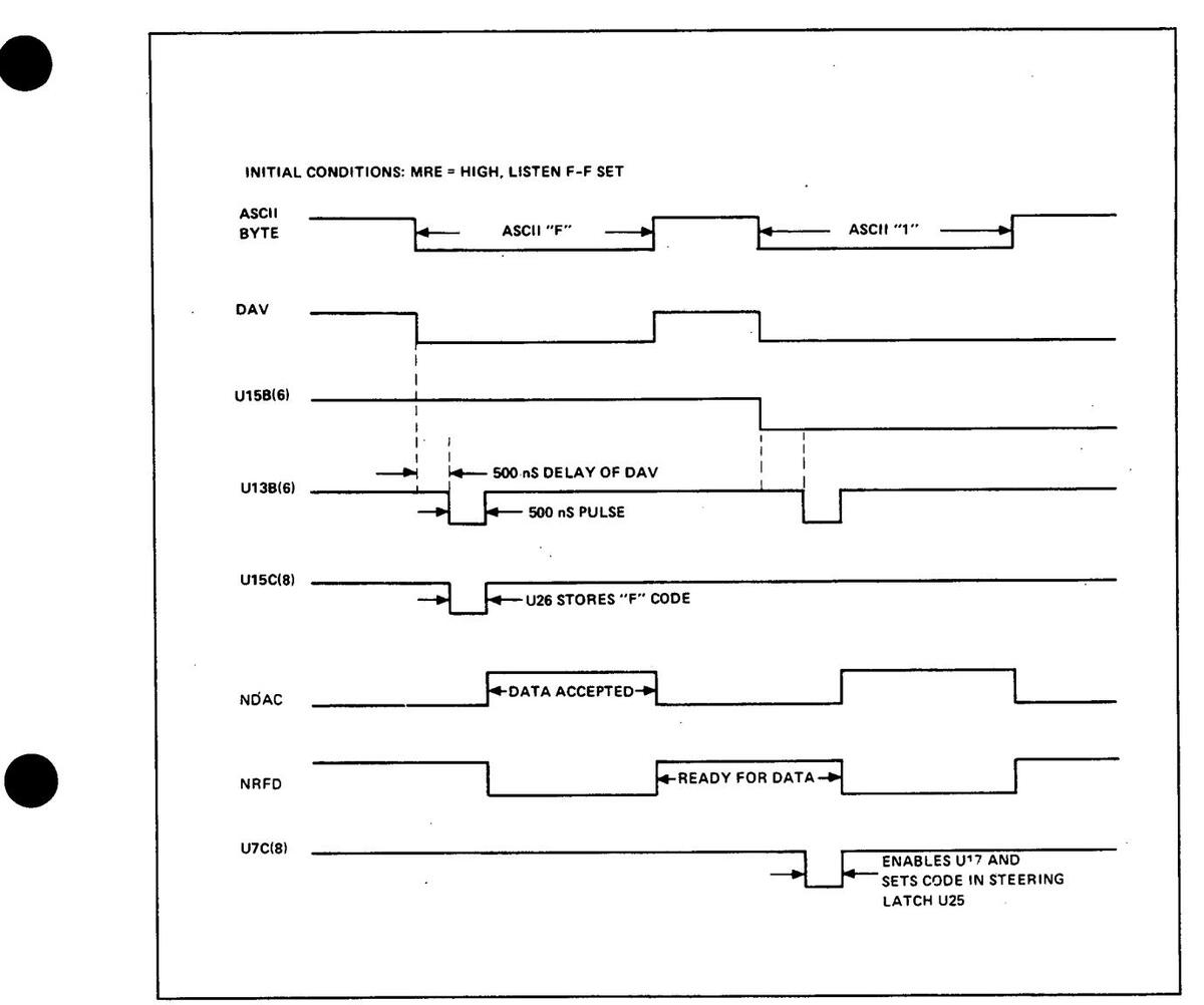
Figure 4-22. Remote Program Timing Diagram
4-191. The controller removes the "F" from the bus, replaces it with an ASCII "1", and pulls DAV Low. This code is used as follows: DI07 is not pulled Use; DI06 and DI05 enable U15B; and DI04 through DI01 are placed on the inputs of the Data Steering Latches. When the delayed DAV signal pulses Low at U13B, it turns on U7C and causes U17 to accept the "F" code that was stored in U26. U17 uses this code to set one of its output lines Low; in this case, it is the 6 line (pin 7) and is used to enable U25 (the function latch). Once enabled, U25 transfers the "1" code to its output lines. Any further changes in the basic program are accomplished in the same manner.
4-192. SWITCHING TO REMOTE. Sometime before the counter makes a measurement, using the newly programmed control settings, it must be switched to remote operation. To do this, the controller sets the REN line Low and sends an ASCII "E8". The "E" enables U16, and the "8" causes U16(4) to go high. This output is NANDed in U8B with the inverted REN signal from U9C. This forces the RMT line Low and sets the counter to follow the remote instructions, instead of the counter's controls. The REN line must remain Low if the counter is to use the functions that were programmed.
4-193. ADDRESSING TO TALK. Before the counter can "talk", it must be cleared from listen. A code of "?" (pro 7 6 5 4 3 2 1 ) enables U21 and disables U4A- When DAV clocks the three flip-flops, the Listen F-F
A12 Option 11 Continued
(6B) returns to its reset state. The counter can now be addressed to "talk". When the Talk F-F sets, the TALK line causes TALK ONLY to go Low, via the switch circuit on A19. This disables U15D and enables U13C (ATN = HIGH). The Low output from U13C (TALK ENABLE), switches the bus terminators from their third state (off or high impedance state) to their active state. Measurement data can now be placed on the bus. U2C(8) sets the SRO line High, indicating to the controller that the counter has data ready.
4-194. The DC SER OUT lines control the order of output data and the state of the ROMs (U29 and U27). Only one ROM is on at any given time. Three of the ROM's outputs (DI07,6, and 5) are sent to the Bus Drivers directly, while the remaining four lines are selected by four-pole switch U28. The ROMs convert the internal data codes to ASCII format. Since the counter is in its out. put routine, the EXT OUT EN line is Low. The FLAG = H line goes High each time a new byte is ready for outputting on the bus. These two lines NAND in U2D to generate a DAV signal. Table 4-2 shows the sequence of data flow to the ROMS, while Tables 4-3 and 4-4 list the ROM codes.
| DC | SER OU | IT | · | ||
|---|---|---|---|---|---|
| С | В | A | DPLR<16 | ENABLED ROM | BUS DATA |
| 0 | 0 | 0 | L | U29 | NONE. Counter is in process of deleting all |
| leading blanks from measurement data | |||||
| before output cycle begins. | |||||
| 0 | 0 | 1 | L | UL29 | DIGIT SIGN. ROM examines SIGN - line to |
| determine polarity of measurement. No | |||||
| ۹. | output if polarity is plus (line = H). | ||||
| 0 | 1 | 0 | L | U29 | DENOMINATOR REGISTER OUTPUT. |
| U28 passes measurement digits contained | |||||
| on DR lines. Blank code (DR C & D=H) | |||||
| causes zero code on bus. | |||||
| 0 | 1 | 0 | Н | U29 | DECIMAL POINT. DPLR<16 line may go |
| High any time during DR output to insert | |||||
| decimal point in output data. | |||||
| 0 | 1 | 1 | L | U29 | "E". Indicates that forthcoming data will |
| be the exponent for power of 10 of | |||||
| - | measure-ment data. | ||||
| | 1 | 0 · | 0 | L | U27 | EXPONENT SIGN. Outputs minus sign to |
| 1 | indicate a number smaller than one; e.g., | ||||
| _ | _ | 6=M, -6=μ. | |||
| | 1 | 0 | 1 | L | U27 | EXPONENT DIGIT. Outputs digit to |
| indicate magnitude of measurement data | |||||
| 0 | Ŧ | TIOO | number. | ||
| 1 | 1 | 0 | L | 029 | CARRIAGE RETURN. Used with tele- |
| printer. Signals end of output. Provides | |||||
| ASCII code to generate teleprinter carriage | |||||
| 1 | 1 | ٦ | 1 | 0011 | return. |
| 1 · | T | T | 1 | 029 | LINE FEED. Used with teleprinter. |
| Provides ASCII code to advance paper to | |||||
| next une. |
Table 4-2. ROM Sequence
4-195. COMPUTER DUMP. Computer Dump causes the Denominator Register and Numerator Register to output data directly from the scalers. When addressed to computer dump, U5B sets and forces the FORCED ARM line Low, via U33B. This line bypasses sample rate and forces the counter to make measurements at its fastest possible rate. The COMP DUMP line goes Low and prevents the counter from entering the arithmetic process.
| IN | PUTS | ; | - | |||||||||||
|---|---|---|---|---|---|---|---|---|---|---|---|---|---|---|
| WORD | BINA | RY SE | LECI | ENABLE | OUT | PUTS | ||||||||
| Е | D | С | B | A | G | 8 | 7 | 6 | 5 | 4 | 3 | 2 | 1 | |
| 0 | L | L | L | L | L | L | L | |||||||
| 1. | L | L | L | L | н | L | L | |||||||
| 2 | L | L | L | н | L | L | L | |||||||
| 3 | L | L | L | Н | н | L | L | |||||||
| 4 | L | L | Н | L | L | L | L | L | L | L | ||||
| 5 | L | L | н | L | н | L | L | L | L | L | ||||
| 6 | L | L | Н | Н | L | L | L | L | L | L | L | L | L | |
| 7 | L | L | н | Н | Н | L | L | L | L | L | L | L | L | |
| 8 | L | н | L | L | L | L | L | L | L | L | ||||
| 9 | L | н | L | L | н | L | L | |||||||
| 10 | L | н | L | н | L | L | L | L | L | L | ||||
| 11 | L | н | L | н | н | L | L | |||||||
| 12 | L | н | н | L | L | L | L | L | L | L | L | |||
| 13 | L | н | н | L | н | · L | L | L | L | L | L | |||
| 14 | L | н | н | н | L | L | L | L | L | L | L | |||
| 15 | L | н | н | н | н | L | L | L | L | L | L | |||
| 16 | н | L | L | L | L | L | ||||||||
| 17 | н | L | L | L | н | L | ||||||||
| 18 | н | L | L | н | L | L | ||||||||
| 19 | н | L | L | н | н | L | ||||||||
| 20 | н | L | н | L | L | L | ||||||||
| 21 | н | L | н | L | н | L | ||||||||
| 22 | н | L | н | н | L | L | ||||||||
| 23 | н | L | н | н | н | L | ||||||||
| 24 | н | н | L | L | L | L | L | L | L | L | L | |||
| 25 | н | н | L | L | н | ·L | L | L | L | L | L | |||
| 26 | н | н | L | н | L | L | L | L | L | L | L | |||
| 27 | н | н | L | н | н | L | L | L | L | L | L | |||
| 28 | н | н | н | L | L | L | L | L | L | L | L | L | ||
| 29 | н | н | н | L | н | L | L | L | L | L | L | L | ||
| 30 | н | н | н | н | L | L | L | L | L | L | L | L | ||
| 31 | н | н | н | н | н | L | L | L | L | L | L | L | ||
| ALL | x | х | x | x | x | н | н | Н | Н | Н | Н | H | Η | Η |
Table 4-3. Rom Outputs , (1816-0254) U29
| . | IN | PUTS | ; | ĺ | |||||||||||
|---|---|---|---|---|---|---|---|---|---|---|---|---|---|---|---|
| WORD | | | BINA | RY SE | r | ENABLE | ||||||||||
| Ε | D | С | В | A | G | 8 | 7 | 6 | 5 | 4 | 3 | 2 | 1 | ||
| 0 | L | L | L | L | L | L | L | L | L | L | / | ||||
| 1 | L | L | L | Ĺ | н | L | L | L | L | L | |||||
| 2 | L | L | L | н | L | L | L | L | L | L | |||||
| 3 | L | L | L | н | Н | L | L | L | L | L | |||||
| 4 | L | L | н | L | L | L | L | L | L | L | |||||
| 5 | L | L | н | L | н | L | L | L | L | L | |||||
| 6 | L | L | н | Н | L | L | L | L | L | L | |||||
| 7 | L | L | н | н | н | L | |||||||||
| 8 | L | Н | L | L | L | L | L | L | L | L | |||||
| 9 | L | Н | L | L | н | L | L | L | L | L | |||||
| 10 | L | Η | L | Н | L | L | L | L | L | L | |||||
| 11 | L | Η | L | Н | Н | L | L | L. | L | L | |||||
| 12 | L | H | н | L | L | L | L | L | L | L | |||||
| 13 | L | Н | н | L | н | L | L | L | L | L | |||||
| 14 | L | Н | н | н | L | L | L | L | L | L | |||||
| 15 | L | н | н | н | Н | L | |||||||||
| 16 | н | L | L | L | L | L | L | L | L | L | |||||
| 17 | н | L | L | L | н | L | L | • | L | L | L | ||||
| 18 | Н | L | L | н | L | L | L | L | L | L | |||||
| 19 | Н | L | L | н | Н | L | L | L | L | L | L | L | |||
| 20 | н | L | н | L | L | L | L | L | L | L | |||||
| 21 | н | L | н | L | н | L | L | L | L | L | |||||
| 22 | н | L | н | н | L | L | L | L | ſ | L | L | ||||
| 23 | н | L | н | н | н | L | |||||||||
| 24 | н | Н | L | L | L | L | L | L | L | L | |||||
| 25 | н | Н | L | L | н | L | L | L | L | L | |||||
| 26 | Н | н | L | н | L | L | L | L | L | L | l | ||||
| 27 | н | н | L | н | н | L | L | L | L | L | L | L | l | ||
| 28 | Н | н | н | L | L | L | L | L | L | L | |||||
| 29 | Н | н | Н | L | н | L | L | L | L | L | |||||
| 30 | н | н | Н | н | L | L | L | L | Į | L | L | ||||
| 31 | н | н | Н | н | н | L | |||||||||
| ALL | X | Х | Х | Х | х | н | Н | н | Н | н | Н | н | Н | Η | |
Table 4-4. ROM Outputs, (1816-0255) U27
4-196. A13 Register. Adder/Subtracter
4-197. The A13 board performs an arithmetic process with the contents of the Event Scaler and Time Scaler. The result of this operation is displayed on the front panel. The board consists of three registers: Numerator, Denominator, and Quotient. Each register contains a Random Access Memory (RAM), having 16 addressable storage locations that are capable of storing 4 bits per location. Data from the Events and Time Scalers are sent to the Numerator and Denominator registers and are then arithmetically manipulated in the Adder/Subtracter circuitry. The Quotient Register (QR) stores the result, while the Quotient Multiplier Counter (QMC) and Multiplier Storage circuitry keep track of the annunciator. The QMC also keeps track of the number of successful subtractions and sends this number to the OR.
4-198. The registers can shift data in the following manner.
Numerator Register
The Numerator register can write data into its RAM from the Time Scaler (A11), Denominator register, or Adder/Subtracter. It can read data out of the RAM into the Adder/Subtracter, Quotient register, or Denominator register.
Denominator Register
The Denominator register can write data into its RAM from the Events Scaler (A11), Quotient register, Numerator register, and Plug-in. It can read data out of the RAM to the plug-in, Adder/Subtracter, Numerator register, display, and output option board, A12.
Quotient Register
The Quotient register can write data into its RAM from the Numerator register, and Quotient Multiplier Counter (QMC). It can read data out of the RAM to the Denominator register, only.
4-199. REGISTER STORAGE OPERATION. The following description concerns an exchange of data between the Numerator Register (NR) and the Denominator Register (DR). The description serves an as explanation for the three registers in general. Each digit of Time Scaler data and Events Scaler data is represented as a 4-bit code. The RAMs are capable of storing 16 of these codes in separate locations (or addresses). The RAM counter that is enabled to count produces a new code with each negative transition of REG CLK. Each new code selects a different RAM location. Once the location is selected, data contained in the location can be read out while REG CLK is Low. If the data source code for the RAM is other than "READ", new data is written into the RAM when REG CLK goes High. Shifting data from one RAM to another requires switches to control the data flow and latches to store data during the write operation. Assuming data has been written into the RAMs from the scalers, a later ROM cycle exchanges data between NR and DR (a frequency measurement). This operation appears as follows.
4-200. The NR EN A and B code changes to "00", and the DR EN A, B, and C code changes to "101". NR CLK EN and DR CLK EN lines are High. This occurs at the start of a new process cycle. REG CLK is Low and data stored at the least-significant-digit (LSD) location appears on the RAM output lines, since the "WE" inputs are High (read mode). The data output of the NR RAM is sent to Latch U20, while the output of the DR RAM is sent to Latch U4 via U1.
4-201. When REG CLK goes High, the data in the latches is locked in, and the outputs of gates U27A and U12B to Low. This last condition forces the RAMs into the "write" mode. The NR RAM writes in the DR data (via (U30) that is stored in U4. The DR RAM writes in the NR data (via U17 and U26) that is stored in U20. When REG CLK goes Low again, U22 and U28 are clocked to a new location code. This process continues until all 16 words have been exchanged. The number of clock pulses (REG CLK) for this process was 16.
| START |
| a 1st ADDRESS 2nd ADDRESS 3rd ADDRESS |
| (DATA READ OUT (DATA WRITTEN |
Figure 4-23. An Exchange of NR and DR Data
4-202. All data entering the registers from the scalers is written into the DR and NR with "LOAD EVENT SCR" and "LOAD TIME SCR" codes on the DR EN lines and NR EN lines, respectively. Data is sent to the Adder/Subtracter circuit during the "READ" portion of REG CLK (Low). The result of each digit subtraction is stored in U4 and in the NR during the "WRITE" portion of REG CLK with a "LOAD A/S" code on the NR EN lines.
4-203. ADD/SUBTRACT CIRCUITRY. This circuit performs an arithmetic operation between the Events Scaler's contents (E) and the contents of the time Scaler (T). The operation is always a division, i.e., either E
for a frequency measurement or E/2XT for a period measurement. The 2EXT/E for a period measurement. The process of division is accomplished by performing a series of subtractions . Under certain conditions this circuit also performs addition (e.g., when the Numerator Register's content is added to itself to double the time count, to recover an overdraft of an unsuccessful subtraction, and during START OR STOP A+B).
4-204. Addition Mode (NR←NR+DR). At the beginning of the process cycle, the ADD line is High and WORD DBL CLK pulses High. Together, the two signals reset U6B via U27D. This sets the initial conditions for the addition: U3 does not receive a carry in (U3 pin 13).
4-205. Assume the circuit is to add 25 and 35. In this example, the registers would appear as:
The 5's are added first. Both 5's are in BCD form and are applied to the A and B inputs of U3 (AD AC AB AA, B0 BC BB BA). The Σ output data is the sum of these two numbers and is expressed in binary .(ΣD ΣC ΣB ΣA) Since the counter circuits operate in BCD only, this code must be converted back to BCD. A second adder, U2, adds a zero when the sum is 0 to 9 and adds 6 when the sum is 10 to 18.


 Loading...