

Page 1

HP Archive
This vintage Hewlett Packard document was
preserved and distributed by
www.hparchive.com
Please
visit
us
on the web !
Scanned by on-line curator: Tony Gerbic
** For FREE Distribution Only ***
Page 2
HEWLETT-PACKARD
COMPANY
4.2A/4.4A
TRAVELING-VVAVE
AMPLIFIER
Page 3

)
)
)
00144·2
OPERATING
AND
SERVICE
MANUAL
MODEL
492A
AND
MODEL
494A
SERIALS
PREFIXED:
010-
TRAVELING-WAVE
AMPLIFIERS
Copy,;gh'
HEWLETT.'ACICA.D
COM'
ANY
1962
lS01
'AGE
MILL
ROAD,
'ALO
ALTO,
CALlFO.NIA,
U.S.A.
Printed:
JAN
1962
Page 4
Model
492Aj494A
Table
of Contents
ListsofIllustrations
and
Tables
TABLE
OF
CONTENTS
Section
Page
Section
Page
I
GENERAL INFORMATION
1-1
IV
PRINCIPLES OF OPERATIO
(cont'd)
1-1.
Description
1-1
4-10.
Traveling
Wave
Tube
4-1
1-6.
Instrument
Identification
1-2
4-15.
Grid
Modulation.
4-4
1-8.
Traveling
Wave
Tube
Warranty
1-2
4-17.
Helix Modulation
·
.
4-4
4-22.
Constant-Amplitude,
Linear
II
INSTALLATION
2-1
Sawtooth
Generator
4-5
2-1.
Mechanical
Inspection
2-1
2-3.
Power
Requirements.
2-1
V
MAINTENANCE.
5-1
2-5.
Power
Cable.
2-1
5-1.
Introduction.
·
5-1
2-8.
Installation
2-1
5-3.
Cleaning
the
Air
Filter·
5-1
2-12.
Repackaging
for
Shipment
2-1
5-5.
Test
Equipment .
5-1
5-7.
Repair.
5-3
III
OPERATING INSTRUCTIONS
3-1
5-8.
Cabinet
Removal
5-3
3-1.
Introduction
.
3-1
5-10.
Tube
Replacement
.
.
5-3
3-3.
Preliminary
Operating
Procedure
3-1
5-12.
Traveling
Wave
Tube
Capsule
3-6.
Helix
Control
3-1
Replacement
5-3
3-8.
Saturation
Power
Output
3-1
5-17.
Changing
the
Frequency
Range
3-12.
Bandwidth
Considerations
.
3-1
of
the
492Aor494A
5-5
3-14.
Constant
GainorConstant
Output
5-21.
Adjustments
5-5
Amplification
3-3
5-22.
Excessive
Helix
Current
5-5
3-18.
Buffer
Amplifications
3-3
5-24.
Chassis
Helix
Control
5-5
3-20.
Amplitude
Modulation
3-3
5-26.
Anode Voltage
Control
.
5-5
3-24.
Pulse
Modulation.
3-6
5-28.
Regulated
Power
Supply
5-5
3-27.
Limited
Phase
Modulation.
3-6
5-30.
Troubleshooting.
·
5-6
3-29.
Unlimited
Phase
Modulation and
5-32.
Performance
Checks
5-7
Frequency
Shifting .
3-6
5-33.
Gain
Check.
5-7
3-34.
Homodyne
Detection
3-7
5-36.
Output
Power
Check
5-7
3-37.
Frequency
Modulation
3-9
5-39.
Noise
Figure
Check
5-7
5-42.
Hum and
Spurious
Modulation Check·
5-8
)
IV
PRINCIPLESOFOPERATION.
4-1
4-1.
Introduction
.
4-1
VI
REPLACEABLE
PARTS
.
6-1
4-3.
Magnet
Power
Supply.
4-1
6-1.
Introduction
6-1
4-5.
Regulated
Power
Supply
4-1
6-4.
Ordering
Information
6-1
LIST
OF
ILLUSTRATIONS
AND
TABLES
Number
Illustration
Title
Page
4-3.
CutawayView
ofaTWT
Capsule
andMagnet
Showing
the
Important
Elements·
. . .
4-3
4-4.
Cutaway View of an
Encapsulated
TWT·
.
4-3
4-5.
Simplified
Circuit
ofa
Constant
Amplitude,
Variable
Slope Sawtooth
Generator··
4-5
5-1.
Top
ViewofModels 492A and 494A
.,
5-2
5-2.
Bottom ViewLooking
Towards
the
Front
PanelofModels
492A and 494A .
..
5-4
5-3.
Rear
View of Models 492A
and
494A"
5-4
5-4.
Test
Setup
for
Gain, Output
Power,
and
Noise
Figure
Performance
Checks
5-7
5-5.
Test
Setup
for
Hum and
Spurious
Modulation
Performance
Check . .
5-8
5-6.
Models 492A and 494A
Schematic
Diagram'
5-9
Number
Illustration
Title
Page
1-1.
Model 492A
Traveling
Wave
Amplifier
1-1
1-2.
Traveling
Wave
Tube
Warranty
1-2
3-1.
Operating
Controls
.
3-0
3-2.
Typical
Gain
and
Power
Output
Characteristics
.
3-2
3-3.
Block
Diagram
of a
Circuit
used
to
Maintain
Constant-Level
Output
Power
fromaTWT
Amplifier
3-3
3-4.
Block
Diagramofan
Automatic
Gain
ControltoMaintain
Constant
Ampli-
fication
from
a TWT
Amplifier
3-3
3-5.
Typical
PlotofOutput VoltagevsGrid
Voltageofa Model 492A
3-4
3-6.
Typical
PlotofOutput VoltagevsGrid
Voltageofa Model 494A.
3-5
3-7.
RF
Phase
Shift
Produced
by Helix Mod
3-7
3-8.
Offset
Frequency
Produced
by Sawtooth
Modulationofthe
Helix .
3-7
3-9.
Block
Diagram
of a
Linear
(Homodyne)
)
Detection
System.
3-8
3-10.
Block
Diagram
of a
CircuittoProduce
an FM Signal with a
TWT
Amplifier
3-8
4-1.
Block
Diagram,
Models 492A and 494A
4-0
4-2.
TWT
and
HowitWorks
.
4-2
00144-2
1-1.
3-1.
5-1.
5-2.
5-3.
6-1.
6-2.
Table
Title
Specifications.
. . . . .
Maximum
Operating
Currents
for
Models
492A and 494A . . .
Recommended
Test
Equipment
Tube
Replacement
List
Troubleshooting
Chart
. . •
Reference
Designation Index
Replaceable
Parts·
. . . .
1-0
3-1
5-1
5-3
5-6
6-2
6-5
iii
Page 5
Section I
Table
1-1
Model 492A/494A
Table
1-1,
Specifications
~ Model 492A
<Fj!
Model 494A
Frequency
Range:
4
gc
to 8
gc
7gcto
12,4
gc
Maximum
Output
Power:
20 mw
minimum
into
50 ohm
load
20 mw
minimum
into
50 ohm load
Modulated
Pulse
Delay:
Approximately
20 ns
Approximately15ns
Helix Modulating Voltage:
Approximately40volts
peak-to-
peak.
Provides
3600phase
shift.
Input
impedance
lOOK
Approximately50volts
peak-to-
peak.
Provides
3600phase
shift.
Input
impedance
lOOK
Hum and
Spurious
Modulation:
At
least
45 db below
signal
level
At
least
45 db below
signal
level
Weight:
Power
Supply:
66
lb
net,
85 Ib shipping
US
volts
±10%, 50to60
cps,
approximately
200
watts
63 Ib net, 84 Ib
shipping
U5
volts
±10%, 50to60
cps,
approximately
225
watts
Accessories
Furnished:
AC-16Q
cable
assembly
AC-l6Q
cable
assembly
For
Both Models
Small
Signal Gain:
30 db
minimum
Meter
Monitors:
Cathode
current,
anode
current,
helix
current,
collector
current.
Input Impedance: 50
ohms,
swr
less
than 2
Output
Internal
Impedance: 50
ohms,
swr
less
than 3
Dimensions:
Cabinet
Mount:
7-3/8
in.wide,
U-l/2
in.high, 20
in.deep.
TypeN
Less
than 30 db
t
:0:
IU]
REAR
,~,,".
:0:
'.1&
1.----19---.,
492AR/494AR
Rack
Mount:
Noise
Figure:
Connectors,
RF
Input and Output:
Pulse
Rise
and Decay
Time:
Amplitude Modulating Voltage:
Approximately15ns
Approximately50volts
peak
positive
pulse
will
produce
a 40 db
change
inrfpower
output.
Sensitivity
approximately1db/volt
1-0
00144-2
Page 6
Model 492A/494A
SECTION
I
GENERAL
INFORMATION
Section I
Paragraphs
1-1to1-4
1-1.
DESCRIPTION.
1-2.
Thet$Models 492A and 494A
Traveling
Wave
Amplifiers
are
broadband,
linear
amplifiers
provid-
ing
adjustable
amplification
up toatleast
30 db,
be-
tween 4 and 12.4 gc, and
haveamaximum
power
out-
put ofatleast20milliwattstoan
external
load
of 50
ohms.
The
frequency
rangeofthet$Model 492A
is
4
to
8 gc; the
frequency
rangeofthe
Model 494A
is
7
to
12.4 gc.
These
traveling
wave tube (twt)
ampli-
fiers
are
designed
to be
used
alsoasbuffer
amplifiers
or
modulators
for
any
signal
within
their
frequency
range.
As
buffers,
their
input
impedances
remain
constant
with any
reasonable
load
changeatthe output
terminal;
the
attenuation between input andoutput
sig-
nalsisat
least
60 db,
minus
the
gain of
the
amplifier.
As
modulators,
they
can
be
usedtoamplitude,
fre-
quency,
pulse,
or
phase
modulate
the
signal
being
amplified
with no
interaction
on
the
signal
source.
The
gain and
power
output of
the
amplifiers
are
con-
tinuously
adjustablebythe
front
panelGRID BIAS
con-
trol.
Hum and
spurious
modulation
generated
within
the
amplifiers
areatleast
45 db below
the
output
sig-
nal
level
and
the
noise
figure
is
less
than 30
db.
1-3.
Thet$Models 492A and 494A
Traveling
Wave
Amplifiers,
amplify
any type ofrfsignal:
cw, swept,
sine-modulated,
pulsed,
multiple
signalsondifferent
frequencies,
etc.
A twt
amplifier
usedasa
modulator,
in conjunction with a
signal
generator,
canbeused
to
amplitude
modulate
anrfcarriertoapproximately
30%
with
less
than 2.5%
harmonic
distortion
and upto50%
with
less
than
5%
distortion.
Amplitude modulation
sensitivityisapproximately1db/volt.
Pulse
modula-
tion
is
excellent;
the
rise
timeisless
than15ns.
Phase
modulation up
to
3600with
less
than 1 db
amplitude
modulation
is
also
possible.
Wide-band
frequency
modulationissimulated
by a
step-wise
phase
modulation
describedinsection
Ill.
1-4.
The
front
panel
meterisprovided
for
checking
and
adjusting
electrode
currentsinthe
traveling-wave
tube.
The
meter
helpstoobtain
desired
operating
characteristics
during
normal
operationofthe
ampli-
fier
and
also
assists
with
preventive
maintenance
and
troubleshooting.
An
anode
voltage
adjustment
on the
instrument
chassis
prOVided
to
adjust
the
cathode
current
of the twt backtonormal
duetotube ageing.
)
00144-2
Figure
1-1.
Model 492A
Traveling
Wave
Amplifier
1-1
Page 7
Section
I
Paragraphs
1-5to1-9
1-5.
The~Model 492A and 494A
are
similarinthat
one
model
maybechangedtothe
other,byreplacing
the
twt,ascoveredinparagraph
5-17.
1-6.
INSTRUMENT
IDENTIFICATION.
1-7.
Hewlett-Packard
usesatwo-section
eight-digit
serial
number
(000-00000).
If
the
first
three
digits
of
the
serial
numberonyour
instrument
do not
agree
WA••ANTY
CLAIM
AND
ADJUITMINT
'IOCIDUU
Model 492A/494A
with
those
on
the
title
pageofthis
manual,
change
sheets
supplied
with
the
manual
will
define
differences
between
your
instrument
and
the
Model 492Aor494A
describedinthis
manual.
1-8.
TRAVELING
WAVE
TUBE
WARRANTY.
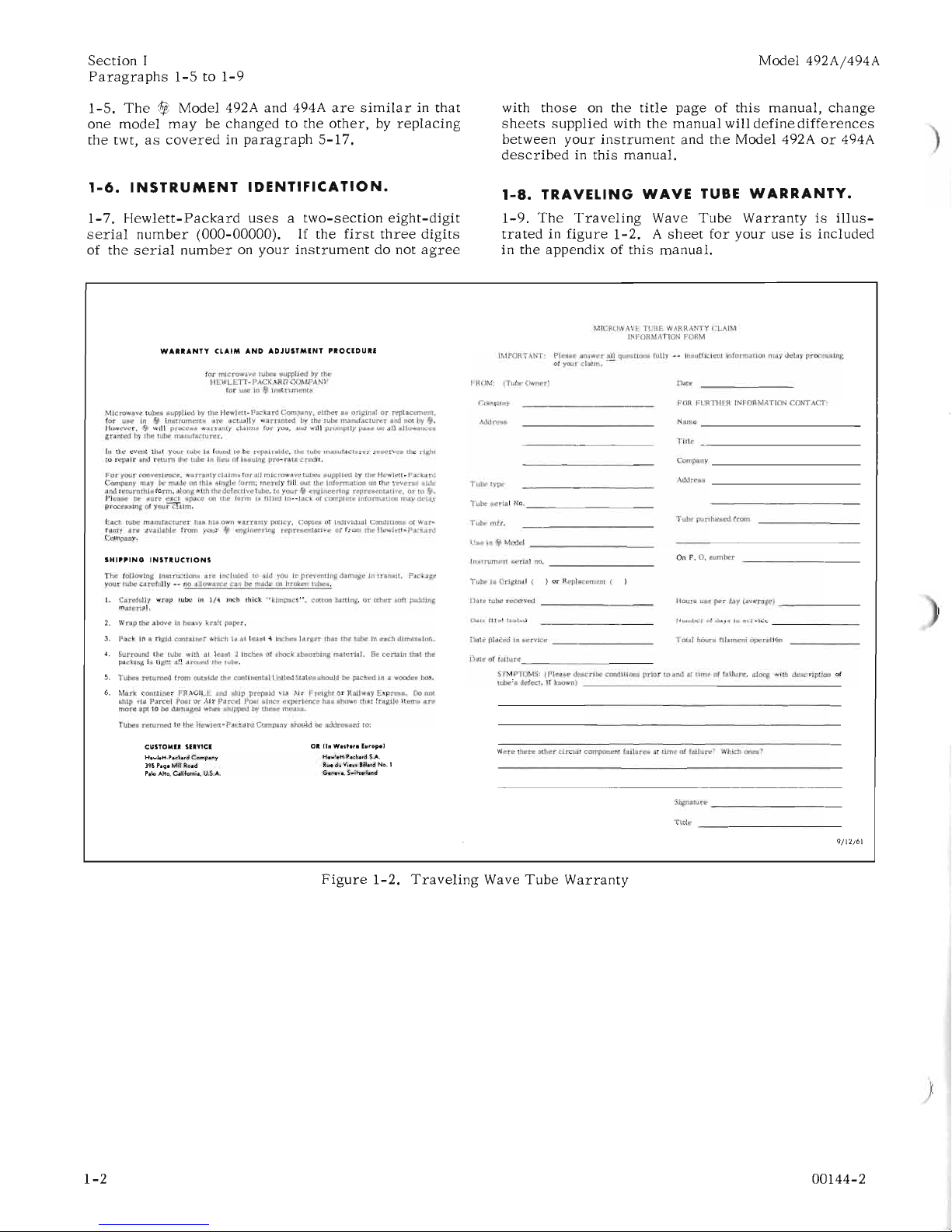
1-9.
The
Traveling
Wave
Tube
Warranty
is
illus-
tratedinfigure
1-2.Asheet
for
your
useisincluded
in
the
appendixofthis
manual.
MICROWAVE
TUBE
WARRANTY CLAIM
INFORMATION FORM
IMPORT
ANT:
Please
ans
....erall
questions
fully--InsuHlclent Information may
delay
processing
of
your
claim.
-
for
microwave
tubes suppliedby[he
HEWLETT·
PACKARD
COMPANY
for
use
In*Instruments
Microwave
tubes
suppliedbythe
Hewlett-Packard
Company.
either88originalorreplacement.
for
use
in8instruments
are
actually
warrantedbythe
tube
manufaclUrer
and
not
by
9.
However, S
will
process
warranty
claims
for
you, and will
promptly
passonall
allowances
grantedbythe
tube
manufacturer.
In
the
event
that
your
tube Is (ound
toberepairable,
the tube
manufacturer
reserves
the
right
to
repair
and
return
the tube in lieu of
Issuing
pro--Tata
credil.
For
your
convenience,
warrantyclalms(orall
microwave
tubes
supplied
by the
Hewlett-Packard
Company
maybemade on
this
sIngle
form;
merely
fJII
out the
lnfonnallon
on the
reverse
side
and
rerurn
this
fonn.
along
....
lth
thedefectlve
rube.toyour8engineering
representallve.
or
tO~.
Pleasebesure
each
space
on the formisfilled
In··lackofcomplete
infonnation
may
delay
processingofyourcTiim.
Each
tube
manufacturer
has
his
own
warranty
policy.
Copies
of Individual Conditions of
War-
ranty
are
available
from
your*engineering
representativeorfrom Ihe He
....
len·Packard
Company.
SHIPPING
INSTIUCTIONS
FROM:
(rube
Owner)
Company
Address
Tube
type
Tube
serial
No.
_
Tube
mfr.
Use
in~Model _
Instrument
serial
no. _
Date
FOR FURTHER INFORMATION CONTACT:
Name
_
Title
_
Company _
Address
_
Tube
purchased
from
OnP.O.
number
The
following
instructions
are
includedtoaid youInpreventing
damageintransit.
Package
your
tube
carefully••no
allowance
canbemade on
broken
tubes.
TubeisOriginal ( )orReplacement
(
1.
Carefully
wrap
tube in
1/4
inch thick
"klmpack".
Cotton batting.orother
sofl
padding
material.
2. Wrap the
above
in heavy
kraft
paper.
3.
Pack
in a
rigid
container
....
hlch Isatleast4inches
larger
than the lube In
each
dimension.
4.
Surround
the
tube
withatleast2inches
of shock
absorbing
material.Becenaln
that the
packing Is tight
all
around
the tube.
Date
tube
received
_
Date
first
tested
Date
placedinservice
_
Dateoffailure
_
Hours
use
per
day
(average)
_
NumberofdaysInservice
_
Total
hours
filament
operation
5.
Tubes
returned
from
outside
the continental
UnltedSrates
shouldbepackedIna wooden box.
6.
Mark
container
FRAGILE and
ship
prepaid
via
Air
FreightorRailway
Expreu.Donot
ship
via
Parcel
POStorAJr
Parcel
POSt
since
experience
has
shown that
fragile
Items
are
more
apttobe
damaged
when
shippedbythese
means.
Tubes
returnedtothe
Hewlen·Packard
Company should be
addressed
to:
SYMPTOMS:
(Please
describe
conditions
priortoandattimeoffailure.
along with
description
of
lube's
defect,
If known) _
CUSTOMr.
snvlcr
H.~".,.d.rd
COfftpel'ly
]95
,.~
Mil
R_d
1'.
Alto. C.lifomi.,
U.S.A.
01
II.W....
,..I.r.,.J
H_lett·,.d.,dS.A.
kvedIiVifillli",dNo.l
G.I'l......S
...
itter!Mtd
Were
there
other
circuit
component
failuresattimeoffailure?
Which ones?
Signature
_
Title
9/12/61
1-2
Figure
1-2.
Traveling
Wave
Tube
Warranty
00144-2
)
Page 8
Model 492A/494A
SECTION
II
INSTALLATION
Section
II
Paragraphs
2-1to2-13
/
2-1.
MECHANICAL
INSPECTION.
2-2.
Unpack
the
instrument
upon
receipt
and
inspect
it
for
signs
of
phy
ical
damage
such
as
scratched
panel
surfaces,
broken
knobs,
etc.
If
thereisany
apparent
damage,
fileaclaim
with
the
carrier
and
refertothe
warranty
pageinthis
manual.
2-3.
POWER
REQUIREMENTS.
2-4.
The
Model 492A and Model 494A
requireapower
source
of
115
volts
± 10%,
single
phase,50to 60
cps,
which
can
deliver
approximately
225
watts.
2-5.
POWER
CABLE.
2-6.
For
the
protection
of
operating
personnel,
the
ational
Electrical
Manufacturers'
Association
(NEMA)
recommends
that
the
instrument
panel
and
cabinet
be
grounded.
This
instrument
is
equipped
with a
three-prong
conductor
power
cable
which, when
plugged
into
an
appropriate
receptacle,
grounds
the
instrument.
The
offset
pin on
the
power
cable
three-
prong
connectoristhe
ground
pin.
2-7.
To
preserve
the
protection
fearure
when
opera-
ting
the
instrument
fromatwo-contact
outlet,
use
a
three-prong
to
two-prong
adapter
and
connect
the
green
pigtailonthe
adaptertoground.
2-8.INST
ALLATION.
2-9.
The
only
special
precaution
necessary
for
in-
stalling
the
twt
amplifiers
is
that
they
should
not be
operated
closetovery
large
magnetic
fields,
such
as
60-cycle
fields,
unless
externally
shielded.
While
the
twt
amplifiers
are
shielded
within
the
cabinet,
complete
protection
against
large
low-frequency
fields
would
require
more
shielding
thanispracticaltoin-
cludeinthe
design.
2-10.
To
operate,
connect
the
instrument
to a
115-
voltacpower
source,
check
and
adjust
rube
operating
00144-2
currents
as
described
in
preliminary
operating
pro-
cedure,
section
1Il, and
connecttothe
external
equip-
ment
with
coaxial
cables
terminatedinstandard
UG-
21D/U,
type
connectors.
2-11.
In
section
V, beginning with
paragraph
5-32,
isalistofperformance
checks
for
this
instrument.
These
procedures
make
a good
testaspartofincom-
ing
quality-control
inspection
following
initial
rurn-on.
2-12.
REPACKAGING
FOR
SHIPMENT.
2-13.
The
following
listisa
general
guide
for
re-
packaging
an
instrument
for
shipment.
If you
have
any
questions,
contact
your
authorized
Hewlett-
Packard
sales
representative.
a.
If
possible,
use
the
original
container
designed
for
the
instrument,
b.
Wrap
the
instrument
in
heavy
paperorplastic
before
placingitin
the
shipping
container.
c.
Use
plentyofpacking
material
around
all
sides
of
the
instrument
and
protect
the
panel
with
card-
board
strips.
d.
Use
heavy
cardboard
carton
or
wooden box to
house
the
instrument
and
use
heavy
tape
or
metal
bandstoseal
the
container.
e.
Mark
the
packing
box with
"Fragile",
"Delicate
Instrument",
etc.
Note
If
the
instrumentistobeshippedtoHewlett-
Packard
Company
for
service
or
repair,
at-
tachtothe
instrumentatag
identifying
the
owner
and
indicating
the
service
or
repair
to
be
accomplished.
In
any
correspondence
be
sure
to
identify
the
instrument
by
model
number,
serial
prefix,
and
serial
number.
2-1
Page 9
Section
III
Figure
1-3
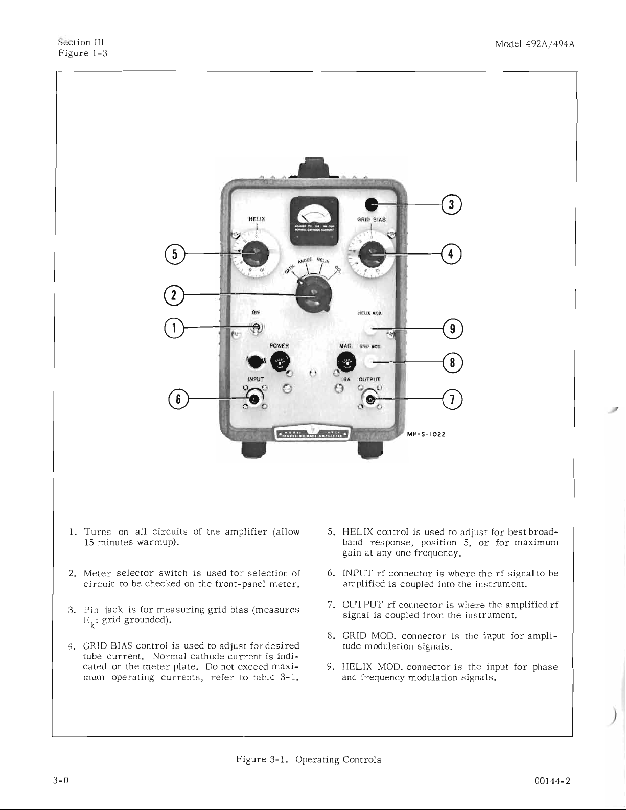
POWER
1.
Turns
on
all
circuits
of
the
amplifier
(allow
IS
minutes
warmup).
2.
Meter
selector
switchisused
for
selection
of
circuittobe
checkedonthe
front-panel
meter.
3.
Pin
jackisfor
measuring
grid
bias
(measures
E
k
;
grid
grounded).
4. GRID BIAS
controlisusedtoadjust
fordesired
tube
current.
Normal
cathode
currentisindi-
cated
on
the
meter
plate.
Do not
exceed
maxi-
mum
operating
currents,
refer
to
table
3-1.
Model 492A/494A
~-~--;3
MAG
C1RJD
Il100
8
7
L
S. HELIX
controlisusedtoadjust
for
best
broad-
band
response,
position
5,
or
for
maximum
gainatanyone
frequency.
6.
INPUTrfconnectoriswhere
therfsignaltobe
amplifiediscoupled
into
the
instrument.
7.
OUTPUTrfconnectoriswhere
the
amplified
rf
signaliscoupled
from
the
instrument.
8. GRID MOD.
connector
is
the
input
for
ampli-
tude
modulation
signals.
9. HELIX MOD.
connectoristhe
input
for
phase
and
frequency
modulation
signals.
3-0
Figure
3-1.
Operating
Controls
00144-2
Page 10
)
Model 492A/494A
SECTION
III
OPERATING
INSTRUCTIONS
Section
III
Paragraphs
3-1to3-13
3-1.
INTRODUCTION.
3-2.
This
section
contains
operating
instructions
for
theModels
492A and 494A
Traveling
WaveTube
Ampli-
fiers.
Figure
3-1
gives
basic
operating
instructions.
The
remainder
of
this
section
supplements
these
in-
structions.
3-3.
PRELIMINARY
OPERATING
PROCEDURE.
3-4.
The
front
panel
controls,
indicator,
and
con-
nectors
for
the
492A and 494A
are
showninfigure
3-1.
This
figure
also
shows
the
uses
for
the
controls,
indi-
cator,
and
connectors.
Whenever
the
twtisturned
on,
use
the
front
panel
metertomeasure
the
current
to
each
electrode
in
the
traveling-wave
tube with
the
GRID BIAS
control
set
for
zero
bias.
The
safe
maxi-
mum
current
for
each
electrodeisshown in
table
3-1.
ormal
cathode
current
for
your
instrumentisindi-
cated
on
the
plate
attached
to
the
meter
face.
Cur-
rents
are
usuallyalittle
high when
the
instrument
is
first
turned
on, but
decreasetonormal
during
warm-
up. Allow IS
minutes
warmup
before
making
final
reading.
The
GRID BIAS
control
maybeusedtore-
duce
the
tube
currents
during
warmup.
Table
3-1.
Maximum
Operating
Currents
for
Models
492A and 494A.
Adjusting
the
HELIX
voltage
control
for
maximum
gainatthe
upper
frequency
limit
usually
produces
the
flattest
frequency
response
over
the
band.
Maximiz-
ing
the
gainatfrequencies
below
the
upper
frequency
limit
usually
resultsinadditional
gain
and
power
out-
put
over
that
obtained
when
adjusted
for
flattest
broad-
band
operation.
The
final
settingofthe
HELIX
con-
trol
is
independentofthe
typeofsignal
amplified.
3-8.
SATURATION
POWER
OUTPUT.
3-9.
Saturation
power
outputisthe
maximum
output
power
obtainable
with a
given
collector
current
and
optimized
helix
voltage.
As
the
input
signal
is
increased
from
the
noise
level,
the
output-vs-input
characteristic
is
linear
until
saturationisapproached
and
the
gain
beginstodecrease.
Eventually
the
output
reachesapeak
whichisthe
saturation
power
output
and any
further
increase
in
the
input
causes
the
outputtodecrease.Ifthe
collector
currentisreduced,
the
power
outputatwhich
saturation
occurs
will be
decreased.
The
primary
effects
which
lead
to
saturation
are:
1)
the
forces
between
the
electrons
in
the
beam
begin
to
limit
the
electron
density
in
the
bunches2)the
energy
transfer
from
the
electron
beamtothe
helix
causes
the
beam
velocitytodecrease
and
gradually
lose
synchronism
with
the
wave on
the
helix.
These
effects
become
more
pronounced
as
saturation
is
approached,
and
cause
the
gainofthe
twttodecrease.
3-6.
HELIX
CONTROL.
3-7.
The
HELIX
voltage
control
on
the
front
panel
maximizes
the
gain
and
power
outputofthe
twtata
selected
frequency
or
optimizes
the
gain
and
power
output
over
the
entire
band;
see
figures
3-2Aand
3-2B.
3-5.
If,
following
tube
replacement,
or
for
some
other
reason,
the
cathode
current
can
be
increased
with
the
GRID BIAS
controltoslightly
above
the
safe
maximum
current
(see
table
3-1),
readjust
the
anode
voltage
control,
paragraph
5-26.
The
anode
voltage
control
is
settolimit
the
twttoits
normal
cathode
current
when
the
bias
voltageonthe
twtiszero.
If
the
cathode
current
is
limitedtoits
normal
value,
but
the
currenttoanother
electrodeisexcessive,
the
amplifier
requires
service
or
adjustment,
see
para-
graphs
5-21or5-30.
)
CAUTION:
DO
NOT EXCEED:
Cathode
current
Helix
current
Collector
current.
Anode
current
3
ma
0.5
ma
3
ma
SO
/la
3-10.
Operating
the
492A
or
494A
near
saturation
power
output will
produce
second
harmonic
content
in
the
output.
To
obtain
maximum
power
output
from
the
twt without
excessive
second
harmonic
contentinthe
output,
increase
the
input
signal
level
until
satura-
tionisreached,
then
reduce
the
input until
the
out-
put
decreases
approximately
6 db (an
input
reduction
of
10
to
15 db).Ifsecond
harmonic
contentisun-
important,
operation
at
saturation
is
usually
very
satisfactory.
3-11.
One
advantageofoperating
the
twt
near
satura-
tionisthe
constant
output
characteristic
exhibited
by
a twt
at
saturation.
At
saturation
the
gain
of a twt
varies
inversely
with
the
input
level
and
input
varia-
tions
of
10 to 15 db
cause
the
outputtovary
only
4
to
6 db.Ifa
more
nearly
constant
outputisdesired,
see
paragraph
3-14.
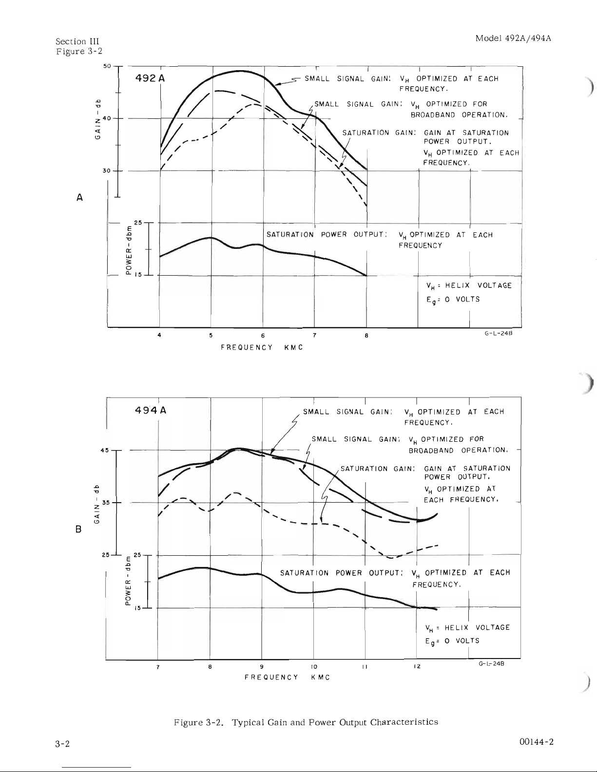
3-12.
BANDWIDTH
CONSIDERATIONS.
3-13.
The
graphsinfigures
3-2A
and B show
typical
gainvsfrequency
and
saturation
power
output
curves
for
the
492A and
the
494A
amplifiers
using
two
differ-
ent
conditions
of
helix
voltage.
One
setofcurves
shows
the
gain
and
saturation
power
output when
the
helix
voltageisoptimizedateach
frequency.
The
other
setofcurves
shows
the
gain
and
saturation
power
out-
put when
the
HELIX
controlissettothe
broadband
00144-2
3-1
Page 11
Section III
Figure
3-2
Model 492A/494A
GAIN:
GAIN AT
SATURATION
POWER
OUTPUT.
VHOPTIMIZED
AT EACH
FREQUENCY.
~
SMALL
SIGNAL
GAIN: VHOPTIMIZED
AT
EACH
FREQUENCY.
SIGNAL
GAIN;
VHOPTIMIZED
FOR
BROADBAND
OPERATION.
SATURATION
POWER
OUTPUT:
VHOPTIMIZED
AT
EACH
FREQUENCY
492A
-rr
a.
15
+-----+-----+-----+--------""'1-----+-----+-------1
50
30
A
V
H
:
HELIX
VOLTAGE
E
o
= 0
VOLTS
4
5
6 7
8
G-L-248
FREQUENCY
KMC
49'4
A
SMALL
SIGNAL
GAIN:
VHOPTIMIZED
AT
EACH
FREQUENCY.
VHOPTIMIZED
FOR
BROADBAND
OPERATION.
SATURATION
POWER
OUTPUT:
VHOPTIMIZED
AT
EACH
FREQUENCY,
GAIN:
GAIN
AT
SATURATION
POWER
OUTPUT
•
V
H
OPTIMIZED
AT
EACH
FREQUENCY.
rr
15
-1-----+-----+-----+-----+----""""""
......
-..---+-------1
25
45
.c
."
I
35
z
«
(9
B
V
H
:
HELIX
VOLTAGE
E
g
:
0
VOLTS
7 8
9 10
II
12
G-L-248
FREQUENCY
KMC
Figure
3-2.
Typical
Gain and
Power
Output
Characteristics
3-2
00144-2
Page 12
Model 492A/494A
Section
III
Paragraphs
3-14to3-22
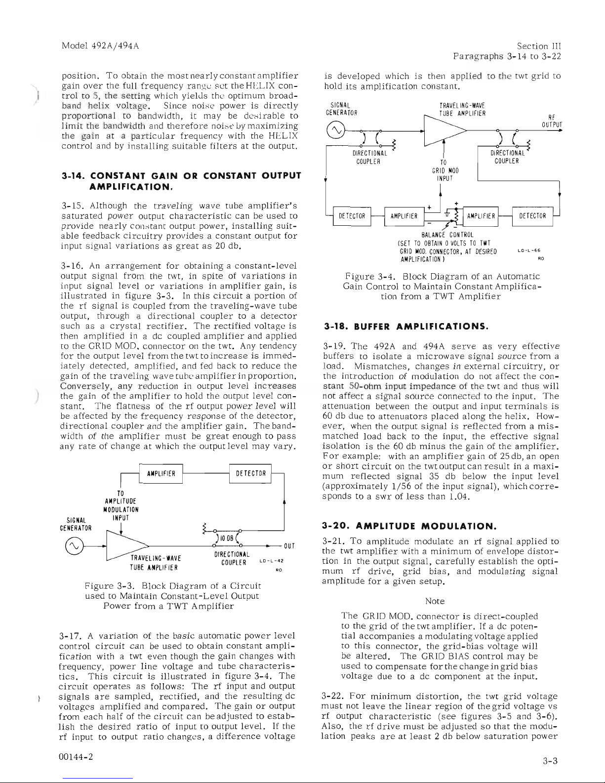
is
developed
whichisthen
appliedtothe
twt
grid
to
hold
its
amplification
constant.
)
pOSltlOn.
To
obtain
the
most
nearly
constant
amplifier
gain
over
the
full
frequency
range
set
the
HELIX
con-
trol
to 5,
the
setting
which
yields
the
optimum
broad-
band
helix
voltage.
Since
noise
powerisdirectly
proportional
to bandwidth,
it
may
be
desirable
to
limit
the
bandwidth and
therefore
noisebymaximizing
the
gain
ataparticular
frequency
with
the
HELIX
control
and by
installing
suitable
filtersatthe output.
3-14.
CONSTANT
GAIN
OR
CONSTANT OUTPUT
AMPLIFICATION.
SIGNAL
GENERATOR
TRAVEL
ING
-WAVE
TUBE
ANPLIflER
TO
GRID
MOD
INPUT
) (
DIRECTIONAL
COUPLER
Rf
OUTPUT
":>--------o------=<o-----+--
OUT
LO-l-66
00
L=J-=-~/~
__
,"""",,---_--,
BALANCE
CONTROL
(SETTOOBTAIN0VOLTSTOTWT
GRID
MOD.
CONNECTOR,ATDESIRED
AMPLIfiCATION)
3-19.
The
492A and 494A
serve
as
very
effective
buffers
to
isolateamicrowave
signal
source
from
a
load.
Mismatches,
changesinexternal
circuitry,
or
the
introductionofmodulation
do not
affect
the
con-
stant
50-ohm
input
impedanceofthe
twt and
thus
will
not
affectasignal
source
connectedtothe
input.
The
attenuation
between
the
output and
input
terminals
is
60 db
duetoattenuators
placed
along
the
helix.
How-
ever,
when
the
output
signalisreflected
fromamis-
matched
load
backtothe
input,
the
effective
signal
isolationisthe
60 db
minus
the
gainofthe
amplifier.
For
example:
withanamplifier
gain
of 25 db,anopen
or
short
circuitonthe
twt
output
can
result
in a
maxi-
mum
reflected
signal
35 db below
the
input
level
(approximately
1/56ofthe
input
signal),
which
corre-
spondstoa
swrofless
than 1.04.
Note
The
GRID MOD.
connectorisdirect-coupled
to
the
gridofthe
twt
amplifier.Ifadcpoten-
tial
accompaniesamodulating
voltage
applied
to
this
connector,
the
grid-bias
voltage
will
be
altered.
The
GRID BIAS
control
may
be
usedtocompensate
for
the
changeingrid
bias
voltage
due
to a
dc
componentatthe
input.
Figure
3-4.
Block
Diagram
of an
Automatic
Gain
ControltoMaintain
Constant
Amplifica-
tion
fromaTWT
Amplifier
3-18.
BUFFER
AMPLIFICATIONS.
3-20.
AMPLITUDE
MODULATION.
3-21.
To
amplitude
modulate
anrfsignal
applied
to
the
twt
amplifier
with a
minimumofenvelope
distor-
tion in
the
output
signal,
carefully
establish
the
opti-
mum
rf
drive,
grid
bias,
and
modulating
signal
amplitude
for
a given
setup.
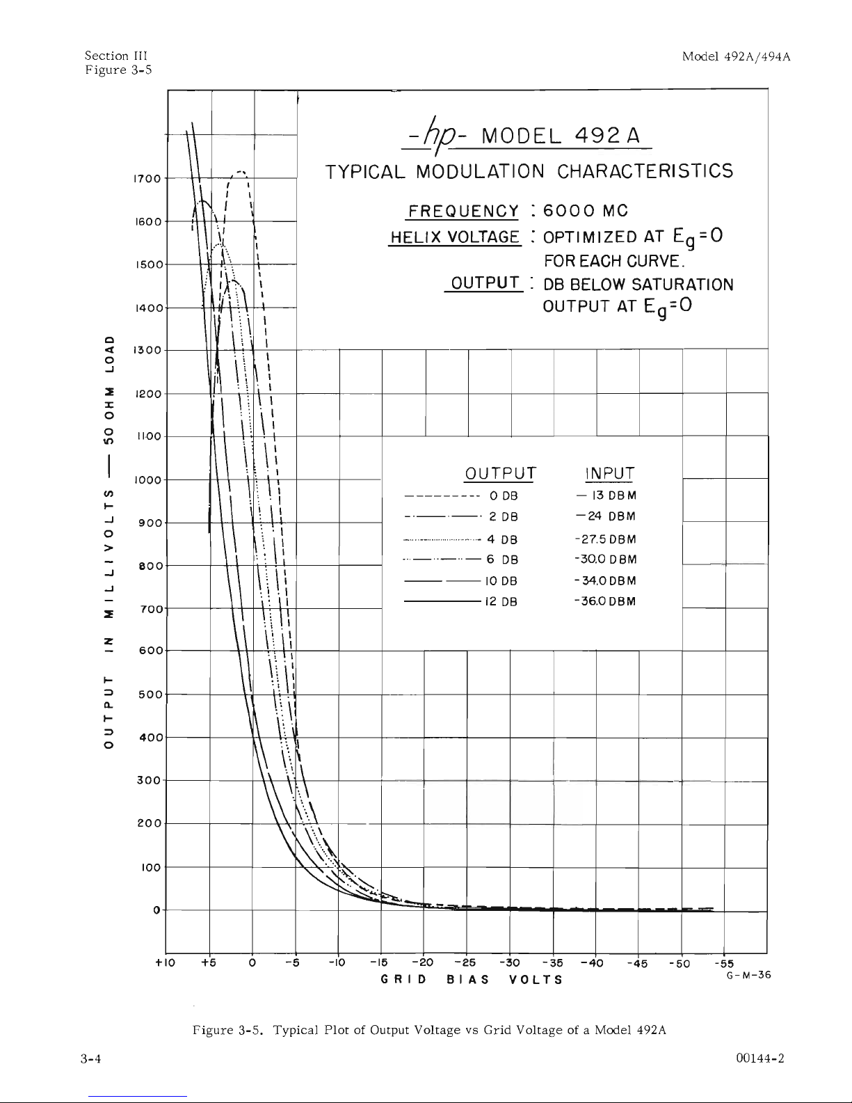
3-22.
For
minimum
distortion,
the
twt
grid
voltage
must
not
leave
the
linear
regionofthe
grid
voltage
vs
rf
output
characteristic
(see
figures
3-5
and
3-6).
Also,
therfdrive
mustbeadjustedsothat
the
modu-
lation
peaks
areatleast
2 db below
saturation
power
DIRECTIONAL
COUPLER
LO-L-'2
00
TRAVELING-WAVE
TUBE
AMPLIfiER
TO
AMPLITUDE
MODULATION
SIGNAL
INPUT
GENERATOR
!
3-15.
Although
the
traveling
wave tube
amplifier's
saturated
power
output
characteristic
canbeused
to
provide
nearly
constant
output
power,
installing
suit-
able
feedback
circuitry
providesaconstant
output
for
input
signal
variationsasgreatas20 db.
Figure
3-3.
Block
Diagram
of a
Circuit
usedtoMaintain
Constant-Level
Output
Power
fromaTWT
Amplifier
3-16.
An
arrangement
for
obtainingaconstant-level
output
signal
from
the twt, in
spiteofvariations
in
input
signal
level
or
variationsinamplifier
gain,
is
illustrated
in
figure
3-3.
In
this
circuitaportion
of
therfsignaliscoupled
from
the
traveling-wave
tube
output,
throughadirectional
coupler
to a
detector
such
asacrystal
rectifier.
The
rectified
voltage
is
then
amplified
in a
dc
coupled
amplifier
and
applied
to
the
GRID MOD.
connectoronthe
twt. Any
tendency
for
the
output
level
from
the
twttoincreaseisimmed-
iately
detected,
amplified,
and fed
backtoreduce
the
gainofthe
traveling
wave tube
amplifierinproportion.
Conversely,
any
reduction
in output
level
increases
the
gainofthe
amplifiertohold
the
output
level
con-
stant.
The
flatnessoftherfoutput
power
level
will
be
affectedbythe
frequency
responseofthe
detector,
directional
coupler
and
the
amplifier
gain.
The
band-
width of the
amplifier
must
be
great
enoughtopass
any
rateofchangeatwhich
the
output
level
may
vary.
3-17.Avariation
of
the
basic
automatic
power
level
control
circuit
canbeusedtoobtain
constant
ampli-
fication
with a twt
even
though
the
gain
changes
with
frequency,
power
line
voltage
and tube
characteris-
tics.
This
circuit
is
illustrated
in
figure
3-4.
The
circuit
operates
as
follows:
Therfinput and output
signals
are
sampled,
rectified,
and
the
resulting
dc
voltages
amplified
and
compared.
The
gainoroutput
from
each
halfofthe
circuit
canbeadjustedtoestab-
lish
the
desired
ratioofinputtooutput
level.Ifthe
rf
input
to output
ratio
changes,adifference
voltage
)
)
00144-2
3-3
Page 13
Section
III
Figure
3-5
Model 492A/494A
\
\,
INPUT
-
13
DBM
-24DBM
-27.5DBM
-30.0DBM
-34.0DBM
-36.0DBM
:
6000
Me
:
OPTIMIZED
AT E
g
=0
FOR
EACH
CURVE.
DB
BELOW SATURATION
OUTPUT AT
Eg=O
OUTPUT
---------
0
DB
-'--'-'
2DB
-_..__
__..- 4
DB
-,,-,,-,,-6
DB
----IODB
----12
DB
OUTPUT
FREQUENCY
HELIX
VOLTAGE
dJp--
MODEL
492
A
TYPICAL
MODULATION
CHARACTERISTICS
\ • I I ,
\\
'\\
'!
I
: .,
\
\'
:
~
\
'\T\TT
\\\\
\\
\'
::
I'
\ !
\ \
~
:
.,
\; \ ,
\ \\\
~
. i ,
\
: ,
I \
1\
,
: ! . ,
"
.~k.
,
r···,
,
I ,
, ,
."
I ,
r,
I
1700
1600
I
1500
1400
0
et
1300
0
..J
~
1200
%:
0
0
11.00
\t)
1000
C/)
~
..J
900
0
>
..J
800
..J
~
700
z
600
~
::)
500
0.
~
::)
400
0
300
200
100
0
+10
+5
o
-5
-10
-15
-20 -25
-30
-35
-40
-45
-50
-55
G
RID
B I A S
VOL
T S
G-
M-36
Figure
3-5.
Typical
Plot
of Output
VoltagevsGrid
Voltageofa Model 492A
3-4
00144-2
Page 14
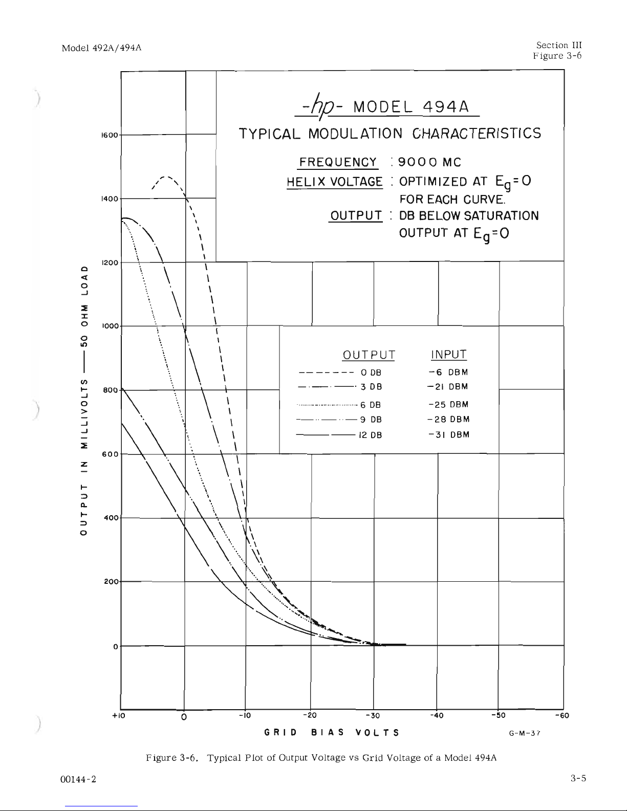
Model 492A/494A
Section III
Figure
3-6
)
1600+-----+-----1
-.::..bp--
MODEL
494A
TYPICAL
MODULATION
CHARACTERISTICS
INPUT
-6
OBM
-21
OBM
-250BM
-280BM
-31
OBM
OUTPUT
-------
0
DB
-'-'-'30B
............- _ 6
DB
-,,-,,-9
DB
----12
DB
FREQUENCY
:
9000
Me
HELIX
VOLTAGE:
OPTIMIZED
AT
Eg=O
FOR
EACH
CURVE.
OUTPUT:DB
BELOW SATURATION
OUTPUT
AT
E
g
=0
\
\
\
\
\
\
\
\
\
,
\
,
,
.
\
\.
\.
,.
.....
,.
,
,.
,
\ \
\
::::".
\'\
" \
\
\
\ \
800
-fI<--------t--\-----J'l---t---1
~\.\
',\
\
I \ \ \ \
6
00
+--4-~.____--+-.:,.-----4---;.-+-----l..-____,r----__r___---......,.....---_+---__l
'.'.
\ \
\>\\
\\
400+-------''rl-----T---'';---+-ir----1-----+-----+-----+----~
\
\.\
..•
',\
\\
.....
1\\
'.
'.
~~
\.
'\
\
..
\
200+------+------>,r-"""'d-....:...;-"""\r----11-----+-----+-----+----~
~~"
.•..
,~~
'~
"~
~
.............
~,.
~:.-.:.:..~
0~---_+_---_+_----1f_--==:..::.!!!~---_+_---_+---___l
1400+------+--~
1200
0
<
0
.J
:E
:I:
0
1000
0
It)
z
V>
~
.J
o
>
.J
.J
)
+10
o
-10
GRID
-20
-30
BIAS
VOLTS
-40
-50
G-M-37
-60
Figure
3-6.
Typical
PlotofOutput
VoltageVBGrid
Voltage
of a Model 494A
00144-2
3-5
Page 15

Section
III
Paragraphs
3-23to3-30
output.
The
linear
modulation
region
extends
from
approximately
+4
volts
(where
beam
de-focusing
occurs)toapproximately
-15
volts
(where
therfout-
put
becomes
an
exponential
function of the
grid
volt-
age).
This
linear
operating
region
permits
upto30%
modulation
with
less
than 2.5%
envelope
distortion
and upto50%
modulation
with
less
than5%distortion.
Envelope
distortion
increases
rapidly
above
50%
modu-
lation.
In
pulse
work
the
twt
maybebiased
near
or
below
cut-off
and
therfdrive
adjusted
for
saturation
outputatthe
peak
amplitudeofthe
modulating
pulse.
However,
the
grid
voltageatthe
peakofthe
modu-
lating
signal
must
not
cause
de-focusing
(approxi-
mately+4to
+ 8
volts)
nor
excessive
average
electrode
current,
see
table
3-1.
The
transient
responseofthe
492A
or
494A to a
step
function
appliedtothe
grid
is
approximately15nsec.
3-23.
Amplitude
modulationisaccompaniedbysome
incidental
phase
modul'btion of
therfsignal,
amount-
ingtoapproximately
90
phase
shiftoftherfcarrier
for
a 10 db
changeinthe
modulatedrfoutput
level.
In
practice
this
phase
modulationisunimportant
when
using
the
conventional
square-law
crystal
detectors,
butisimportantindetection
systems
where
the
out-
putisa functionoftherfcarrier
phase.
3-24.
PULSE
MODULATION.
3-25.
Thereisconsiderably
latitudeinthe
adjustment
of
modulation
characteristics
when
pulse
modulating
anrfsignal
using
the
492Aorthe
494A;
see
figures
3-5
and
3-6.
The
cw
input
level,
the
modulation-
pulse
amplitude,
and
the
grid
bias
determine
the
characteristics
of
the
rf
output
pulse
as
follows:
a.
The
cw
input
signal
primarily
determines
the
maximum
possible
leveloftherfoutput
pulse
and
whetherornot
the
twt
canbeoperated
into
saturation.
b.
The
peak-to-peak
amplitudeofthe
modulating
pulse
primarily
determines
the
on-off
ratioofthe
rf
output
pulse.
c.
The
grid
bias
level
primarily
determines
the
rf
output
levels
attained
during
the
pulse-on
and
pulse-
off
times
and
also,inconjunction
with
the
modulating
pulse,
determines
the
rf
input
level
necessary
to
saturate
the
twt.
The
GRID BIAS
control
always
should
be
set
so
that
the
twt
grid
will not
draw
cur-
rent
(approximately4volts
positive)
during
the
pulse-
on
period.
3-26.
To
pulse
modulate
therfsignal
being
amplified
in
the
492A
or
494A,
refer
to
figures
3-5or3-6
and
proceedasfollows:
a.
Determineifthe
twtisto be
driven
into
satura-
tion
andiftherfoutput
mustbeataspecific
level.
b.
Set
the
GRID BIAS
control
for
zero
bias.
c.
Connect
therfinput
signaltothe
twt and
adjust
its
leveltoproduce
the
desiredrfpulse
output
level.
d.
Determine
the
on-off
voltage
ratio
required
in
therfoutput
pulse.
3-6
Model 492A/494A
e.
Using
the
graph
in
figure
3-5
determine
the
magnitudeofmodulation
pulse
requiredtoproduce
the
desired
on-off
ratio.
f.
Set
the
GRID BIAS
controltoobtain
the
voltage
determined
in
step
e.,
Le.,
the
peak
voltageofthe
modulating
pulse.
The
bias
VOltage
maybemeasured
at
the
pin
jackonthe
front
panel.
g.
Connect
the
modulating
pulsetothe
GRID MOD.
connector
and
adjust
its
amplitudetothe
voltage
de-
terminedinstep
e to
produce
the
desired
on-off
ratio
in
therfoutput
pulse.
Since
the
gridofthe
twtiscon-
nected
directly
to
the
GRID MOD.
jack,adc
com-
ponent
in
the
modulating
signal
will
affect
the
grid
bias.
Also,ifcapacitive
couplingisused
the
modu-
lating
signal
will
drive
the
gridofthe
twt
above
and
below
the
dc
level
established
by
the
grid
bias,
an
amount
determined
by
the
duty
cycleofthe
modulating
signal.
The
GRID BIAS
control
mustbeadjusted
to
compensate
for
both of
these
effects.
h.
To
increase
the
on-off
ratiooftherfoutput
pulse,
increase
the
amplitudeofthe
modulation
pulse,
at
the
same
time
adjust
the
grid
biassothat
the
grid
will not be
driven
beyond 4
volts
positive,
see
the
Note
paragraph
3-21.
Note
Large
input
modulating
pulses,
above
15
volts,
tendtoshock-excite
the
helix,
produc-
ing
ringing
on
the
top of
therfoutput
pulse
and a slow
rise
time.Ifthe
traveling-wave
tubeisoperated
near
saturation
this
effect
is
minimized
and
better
pulse
characteristics
are
obtained.
3-27.
LIMITED
PHASE
MODULATION.
3-28.
The
signal
being
amplifiedinthe
492Aor494A
can
be
phase-modulated
by applying
voltagetothe
HELIX MOD.
connector.
This
voltage
varies
the
electron-beam
velocity
by
changing
the
potential
be-
tween
the
cathode
and
the
helix--a
positive
voltage
change
accelerates
the
electron
bunches
and
advances
the
phaseoftherfoutput
signal;anegative
change
slows
them
and
retards
the
phaseofthe
output
signal.
The
resultant
phase
deviationinthe
output
signal
is
directly
proportionaltothe
applied
voltage.
The
de-
gree
of
phase
deviation
producedislimited
by
the
range
of
helix
voltages
that
produces
amplification,
and
by
the
amountofincidental
amplitude
modulation
permissible
in
therfoutput.
Phase
deviation
of 360
0
is
possible
with
the
output
amplitude
heldtovariations
of
approximately
1-1/2
db andisobtained
with a
helix
voltage
variationofless
than 50
volts.
The
actual
voltage
required
foraphase
shiftof3600varies
with
the
operating
frequency
and
from
tube-to-tube.
3-29.
UNLIMITED
PHASE
MODULATION
AND
FREQUENCY
SHIFTING.
3-30.
Although
the
limited
phase
deviation
described
in
paragraph
3-27isusefulinsome
applications,
un-
limited
phase
deviation
hasamuch
wider
range
of
usage.
Itisparticularly
useful
because
the
frequency
00144-2
Page 16

Model 492A/494A
Section III
Paragraphs
3-31to3-36
G-l-7
TIM
E
DESIRED OUTPUT
(Ftl
FR
EQU
ENCY +-
__
-'---_----'
__
---A.
__
--L.._---l
--
---
---1---
INPUT FREQUENCY
(Fl
UNDESIRED OUTPUT ( F )
FREQUENCY
2
HIGH
Figure
3-8.
Offset
Frequency
Produced
by
Sawtooth Modulation of
the
Helix
LOW
SAWTOOTH MODULATION
APPLIED
TO
HELIX
3-31.Inpractical
applications,aconstant
amplitude
linear-slope
sawtooth
generator
is
used to
produce
the
sawtooth
waveforms.Ifthe
amplitude8fthe
saw-
tooth
voltageisadjustedtoproduce
a 360
shift,
one
cycle
of
the
cw
signal
will be addedorsubtracted
during
each
sawtooth, and
the
frequency
shift
pro-
duced in
the
output will be
equaltothe sawtooth
repe-
tition
rate.
Sawtooth
voltages
having
negative
slopes
(see
figure
3-7)
produceadecrease
in the output
fre-
quency (delay in
phase).
Conversely,
sawtooth
volt-
ages
of the
opposite
slope
causeanincreaseinoutput
frequency.
of the input
signal
canbeshifted
by a
predetermined
amount. Unlimited
phase
deviationiseffectively
sim-
ulated
by continuously
repeating
exact
3600phase
deviations.
Thisisaccomplished
by modulating
the
traveling
wave tube
helix
wiSh
a sawtooth
waveform,
each
sawtooth
producing
360
phase
shift,asshown
in
figure
3-7.
Anrfoutput
frequency
thatisshifted
in
relationtothe input
frequencyisthus produced,
as
shown in
figure
3-8.
O·
HIGH
SAWTOOTH
MODULATION
APPLIED
TO
HELIX
LOW
PHASE DIFFERENCE
BETWEEN
INPUT AND
OUTPUT WAVES
frequency
shift
with
its
relatively
small
power
content
would
be
rejected
by
most
narrow
band
circuits.
In
systems
where
the
undesired
frequency
shift
falls
within
the
pass
band of the
equipment
under
test,
a
negative
pulse
canbeappliedtothe
GRID MOD.
con-
nectortocut
off the twt
beam
current
during
the
fly-
back
time.
This
method
reduces
the
undesired
fre-
quency
shift
althoughitproduces
some
small
tran-
sients
and
leaves
small
time
intervals
during
which
thereisno
signal
output.
Practical
applications
of
offset
frequencies
include
the
measurement
of
ex-
tremely
high
swr's
accurate
calibrationofattenu-
ators
over
wide
amplitude
ranges
(paragraph
3-34),
frequency
shiftingofmicrowave
radio
relay
channels
for
retransmission,
productionofmixer
frequencies
for
radar
and
other
microwave
receivers,
etc.
G-l-I
TI
ME
..
3-34.
HOMODYNE
DETECTION.
Figure
3-7.
RF
Phase
Shift
Produced
by
Helix Modulation
3-32.
With sawtooth modulation,
the
desired
output
frequency
shift
(F
in
figure
3-8)
occurs
during
the
sawtooth
formatioJ
time,
andisproportional
to
the
rate
of
change
of voltage.
During
the sawtooth
fly-
back
time
the output
phaseisshifted
in the
opposite
direction
producinganundesired
frequency
shift(F2
in
figure
3-8).Ifthe
flyback
timeismade
extremely
short,
this
frequencyisfar
removed
from
the
desired
frequency
since
the
degreeoffrequency
shiftisin-
versely
proportionaltothe
flyback
time.
In
addition
to
being
far
removed
from
the
desired
frequency
the
powerinthe
undesired
frequencyisvery
small
since
itisproportionaltothe
ratio
of flyback
timetosaw-
tooth
time.
3-33.Ina
typical
case
involving a
desired
50-kc
fre-
quency
shift,
a
I-microsecond
flyback
time
would
produceaI-megacycle
frequency
shiftinthe
opposite
direction
and would
contain
only5%of
the
total
power
in
the
output wave.
In
practice,
this
undesired
3-35.
The
ability
of a twttoproduce
an
offset
fre-
quency
thatisstable
with
respecttothe
signal
source
makesitan
ideal
instrument
to
use
in a homodyne
(linear)
detection
system.
The
difference
frequency
will be dependent upon
the
stability
of the sawtooth
generator
usedtomodulate
the
twt helix, a
problem
ofnoconsequenceatthe
low modulating
frequencies
involved.
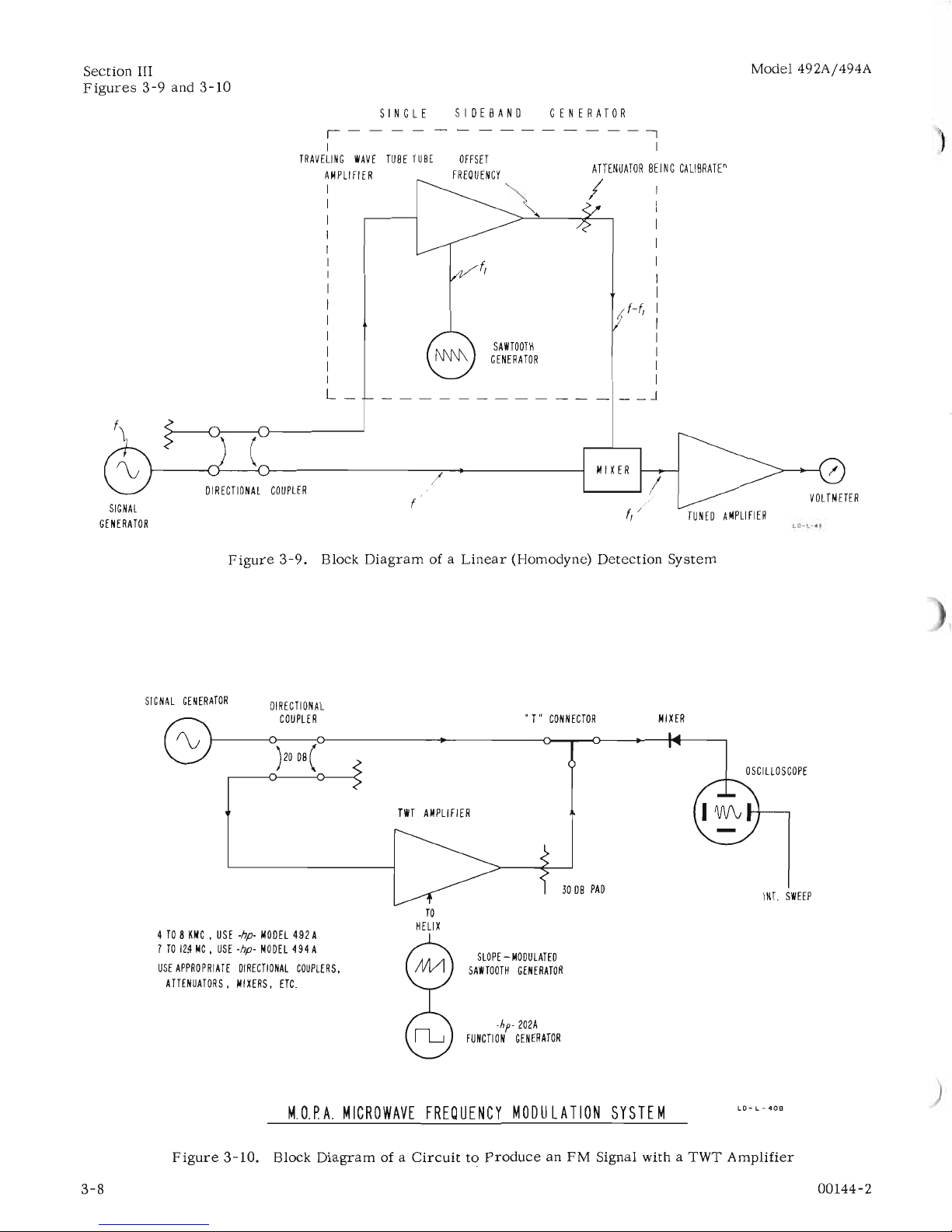
3-36.Atypical
linear
detector
system
suitable
for
calibrating
microwave
attenuators
is
illustrated
in
figure
3-9.
The
signal
generator
suppliesasignal
(f) both
toacrystal
mixer
andtoa
traveling
wave
tube
amplifier.
The
traveling
wave tube
amplifier
is
sawtooth modulated to
produce
an
offset
frequency
(f-f
) whichisapplied to
the
attenuatortobe
cali-
brated.
The
output
signal
from
the
attenuatoristhen
combined
with the
original
signal
(f) in
the
mixer
to
produceabeat
frequency
(f ) whose
amplitudeisdi-
rectly
proportional
to
the
ahtplitudeof(f-f
j
)
so
long
as
the
amplitudeof(f-f
j
)
remains
within
the
square-
law
region
of the
cryStal.
This
beat
frequency
is
amplified
by
the
tuned
amplifier
and
the
outputisin-
dicated
by an
ac
voltmeter.
The
lower
sensitivity
01144-2
3-7
Page 17
Section III
Figures
3-9
and
3-10
Model 492A/494A
SAWTOOTH
GENERATOR
f,
OFFSET
FREQUENCY
SINGLE
SIDEBAND
GENERATOR
-------------1
I
A
TTENUATORBEING
CALIBRATE"
/ I
I
I
I
I
I
I
f-f, I
I
I
I
I
I
_
_J
L_
I-
I
TRAVELING
WAVE
TUBE
TUBE
AMPLIFIER
SIGNAL
GENERATOR
COUPLER
/
f
VOLTMETER
TUNED
AMPLIFIER
LO-l-'"
Figure
3-9.
Block
Diagram
of a
Linear
(Homodyne)
Detection
System
INT.
SWEEP
OSCILLOSCOPE
MI
XER
30
DB
PAO
'T'
CONNECTOR
TWT
AMPLIFIER
)20OB(
DIRECTIONAL
COUPLER
SIGNAL
GENERATOR
4TO8
KNC0USE
-hp-
MODEL
492
A
7TO12.4
MC.
USE
·hp·
MODEL
494
A
USE
APPROPRIATE
DIRECTIONAL
COUPLERS.
ATTENUATORS.
MIXERS.
ETC.
TO
HELIX
SLOPE-MODULATED
SAWTOOTH
GENERATOR
.h
p
'
202A
FUNCTION
GENERATOR
M.O.P.A.
MICROWAVE
FREQUENCY
MODULATION
SYSTEM
LD-L-40B
Figure
3-10.
Block
Diagramofa
Circuit
tc?
ProduceanFM
Signal with a TWT
Amplifier
3-8
00144-2
Page 18

)
Model
492A/494A
limitisdetermined
by
the
crystal
and IF
amplifier
noise
andisapproximately
-100
dbm.
ote
When a
swr
indicator
(suchasthe
<[j)
Model
4158)
calibrated
for
use
with a
square-
law
detector
is
usedinplaceofthe
tuned
amplifier
and
voltmeter,
the
db
readings
mustbedoubled.
3-37.
FREQUENCY
MODULATION.
3-38.
Narrow-band
frequency
modulation
canbeob-
tained
by
applying
the
modulation
signal
directly
to
the
helixofthe
twt;
however,tofrequency
modulate
with an
appreciable
frequency
deviationitis
first
necessarytoproduceanoffset
frequencyasdescribed
in
paragraph
3-29.
The
deviationofthe
offset
fre-
quency
shouldbeslightly
greater
than
1/2
the
total
frequency
deviation
desired.
The
offset
frequency
is
then
varied
by
varying
the
slope
of
the
sawtooth.
3-39.Asawtooth
waveform
produced
by
the
special
generator
describedinparagraph
4-20
canbeslope-
00144-2
Section
1II
Paragraphs
3-37to3-40
modulated
by any
waveform
before
being
applied
to
the
traveling
wave
tube
helix.Inthis
manner
complex
signals
canbeusedtofrequency-modulate
the
signal
applied
to
the
twt and
the
center
of
the
output
fre-
quency
will
be
fixed by
the
sawtooth
repetition
rate
without
slope
modulation.
Innocase
should
the
p~ase
shift
duetoa
single
sawtooth
cycle
exceed
360
so
that
the
amplification
propertiesofthe
traveling
wave
tube
amplifier
will notbeadversely
affected
regard-
less
of
the
magnitudeofthe
apparent
phase
deviation
when
the
sawtooth
waveismodulated.
3-40.
Figure
3-10isa
block
diagram
of a
system
for
the
generationoffrequency-modulated
offset
signals.
In
this
arrangement,
the
slope-modulated
sawtooth
voltage
whichisappliedtothe
twt
helix
produces
an
offset
frequency,
the
instantaneous
frequencyofwhich
is
proportionaltothe
slopeofthe
sawtooth.
Varying
the
slopeofthe
sawtooth
voltage
varies
the
offset
fre-
quency.
Thus
the
output
signal
from
the
twtisan
fm
signal.
The
detected
fm
signal
(the
difference
between
the
signal
generator
frequency
and
the
fre-
quency-modulated
offset
frequency)
is
shown on
the
oscilloscope.
3-9
Page 19

"'"
,
o
'rjC/)
.....
CD
OQ
n
c:
~.
'i
0
CD
::s
"'"-
,<
......
3::
8.
CD
>-
"'"
'Cl
N
;>
-....
"'"
'Cl
"'"
;>
J4
rG'iiiDl
l!QQJ
J5
PIN
JACK
ON
FRONT
PANEL
FOR
MEASURING
BIAS
J2mD
J3m
(
~Jll
HELlXI
MOO.
Figure
4-1.
Block
Diagram
~
Models
492A and 494A
~
-
SRI
HALF
WAVE
RECTIFI
ER
+
SR2
~
VI
V5A
SR3
SERIES
HELIX
VOLTAGE
REGULATOR
MODULATOR
I
DOUBLER
6BQ6
V4
1126BQ7A
REFERENCE
ew
I
-
VOLTAGE
I
HELIX
~
0
OA2
STRAY
CAPACITY
'--c.--
T1
V2
V5B
..,-
,,'
-",
CONTROL
DISCHARGE
I I
POWER
TUBE
TUBE
,
,
I
i
~
TRANSFORMER
6AU6
1
12
6BQ7A
IWI
~
I
I
elY
-
:
~
u
> <
@
HELIX
e>
elY
I
-
--
I
""
ANODE
\~.J
~
, "
'--
""
~
<
V3
~o
I
GRID
BIAS
I
<:>
BIAS
eIY~
REGULATOR
OB2
80-
L-44B
JF1
I.SA
F2
1.6
A
~
SR4
~
TIT
MAGNET
SI
SUPPLY
L----J
L-
o
o
......
"'"
"'"
,
N
Page 20

)
Model 492A/494A
SECTION
IV
PRINCIPLES
OF
OPERATION
Section
IV
Paragraphs
4-1to4-13
)
)
4-1.
INTRODUCTION.
4-2.
The
twt
amplifier
contains
very little
signal
cir-
cuitry
external
to
the
twt
itself.
The
electrical
cir-
cuitsinthe
instrument
provide
the
operating
voltages
and
the
means
for
modulating
the
twt,asshown in
the
block
diagram,
figure
4-1.
4-3.
MAGNET
POWER
SUPPLY.
4-4.
The
492A and 494A
utilizea400-gauss
electro-
magnet
(surrounding
the
traveling
wave tube
capsule)
to hold
the
emitted
electrons
in a
very
narrow
beam.
The
power
supply
for
the
magnet
consists
of a
full-
wave
selenium
bridge
rectifier
connected
directly
across
the
US-volt
line
andacapacitive-input
filter,
and
supplies
approximately
0.7
ampere
at
an output
voltage
of 120
voltsdcwith
less
than 1 volt
rms
ripple
when
connectedtothe
magnet.
The
magnetiscovered
by a
shield
asaprotection
against
stray
magnetic
fields.
4-5.
REGULATED
POWER
SUPPLY.
4-6.
The
operating
voltages
appliedtothe
twt
are
obtained
fromavoltage
doubler
followed by a
voltage
regulator,
VI,
V2, and V4.
The
regulationisaccom-
plished
by
varying
the
plate
resistance
ofVIin
ac-
cordance
with
the
output
voltageinthe
following
man-
ner,
see
figure
4-1.
V4isa
constant
voltage
tube
which
holds
the
voltageatthe
gridofV2
constant
with
respect
to
the
cathodeofVI.
The
cathodeofV2
is
connectedtoa
voltage
divider
between
the
cathode
of
VI
and
the
minus
sideofthe
supply.Ifthe
cathode
voltageofVI
increases,
the
grid
voltageofV2
will
also
increase
the
same
amount.
However,
the
cath-
ode
voltage
of
V2
will
increase
only by
an
amount
equaltothe
ratioofresistance
below
the
potentiom-
eter
arm
to
the
total
resistance
times
the
total
voltage
change.
Thus,asignal
appears
on the
grid
of
V2
whichisproportionaltothe
riseofvoltage
on
the
cathodeofVI.
This
signal
on the
grid
of V2
is
amplified
and
inverted
by
V2
and
appliedtothe
grid
of V1,
increasing
the
plate
resistance
of V1 and
low-
ering
the
voltageatthe
cathodeofVI
which
results
in
a
substantially
constant
output
voltage.Ifthe
voltage
at
the
cathodeofVI
tendstodecrease,
the
plate
re-
sistanceofVI
decreases,
holding the
voltageatthe
cathode
of V1
substantially
constant.
4-7.
The
chassis
Helix
control
(R25)
adjusts
the
level
of
the
regulateddcoutputtocompensate
for
the
varia-
tions
in twt
characteristics.
The
switch,
52,
and
the
associated
voltage
dividers
permit
the
useofthe
same
power
supply
with two twt
types
and
allows
the
opera-
tor
to
use
the
same
instrumentasa 492A
(4-8
gc)
or
as
a 494A
(7-12.4
gc) by
changing
the twt. Changing
the
tube typeisno
more
difficult
than
replacing
the
twt
with
another
tube of
the
same
type
(see
para.
5-17).
00144-2
4-8.
The
bias
voltage
for
the
twtissuppliedbyV3
and
controlled
by the GRID BIAS
controlonthe
front
panel.
The
grid
of
the
twtisgrounded
through
a
3900-ohm
resistor,
and
the
voltageonthe
cathode
is
varied.
The
circuit
is
arranged
so
that
all
the twt
electrode
voltages
except
the
control
grid
varyasthe
cathode
voltageisvaried
and
therefore
remain
con-
stant
with
respecttothe
twt
cathode.Ifthe
grid
were
not
grounded,
but
connectedtoa
sourceofvariable
negative
voltage
a blocking
capacitor
wouldberequired
which would
impair
the
response
of the twttolow-
frequency
modulating
signals.
A pin
jackonthe
front
panel
allows
the
bias
voltagetobe
measured;
an
ex-
ternal
voltmeter
haVing 20,000
ohm/volt
sensitivity
or
higher
shouldbeused.
4-9.
The
anode
voltageiscontrolled
by a
potentiom-
eter
on
the
chassisofthe
instrument
andisadjusted
to
obtain
normal
cathode
current
for
the
twt
amplifier;
see
paragraph
5-26.
The
front
panel HELIX
control
adjusts
the
helix
voltageofthe
twt to obtain
either
maximum
gain and
powerata
particular
frequency
or
optimum
broadband
response.
4-10.
TRAVELING
WAVE
TUBE.
4-11.
The
basic
traveling
wave
tube
consists
of an
electron
gun which
projectsafocused
electron
beam
throughahelically-wound
coiltoa
collector
electrode,
shown in
figure
4-3.
The
focused
electrons
are
held
inapin-like
beam
through
the
centerofthe
helix
by
a powerful
magnet
around
thefull lengthof
the
capsule.
4-12.
A cw
signal
coupled
into
the
input
end of the
helix
travels
around
the
turnsofthe
helix
and
thus
has
its
linear
velocity
reducedbythe
amount
equaltothe
ratio
of
the
length of
wire
in the
helixtothe
axial
lengthofthe
helix.
The
electron
beam
velocity,
de-
termined
by the
potential
difference
between
thecath-
ode
and
the
helixisadjustedsothat
the
electron
beam
travelsalittle
faster
than the cw
signal.
The
electric
field of
the
cw
signal
on the
helix
interacts
with
the
electric
field
created
by
the
electron
beam
and
in-
creases
the
amplitudeofthe
signal
on the
helix,
thus
producing
the
desired
amplification.
4-13.
Figure
4-2isa
diagram
showing the
principal
elements
of a
typical
traveling
wave
tube
in the
upper
portion
and
the
important
stepsinthe
amplification
processinthe
lower
portion.
The
steps
shouldbefol-
lowed by
referring
to
the
numbered
captions
below.
(1)
An
electron
beamisdirected
through
the
center
of
the
helix.
(2) A cw
signaliscoupled
into
the
helix.
Arrows
in
the
detail
show the
direction
and
magnitudeofforce
exerted
on
the
electron
beam
by
the
cw
signal.
4-1
Page 21

"'"
I
t-;)
BEAM
FORMING
ANODE
200V
TO
300
V
,.---
HELIX
MOUNTING
AND
SHIELD
VOLTAGE
SANE
AS
COLLECTOR
LOSSY
-
WIRE.
HELIX
-COUPLED
ATTENUATOR
COLLECTOR
FRON
500
V
TO
1500
V
(DEPENDING
ON
TUBE
TYPEl
'TjUl
....
(1)
OQO
C M
I-l ....
(1) g
"'"
......
~<
INPUT
DIRECTIONAL
COUPLER
SINGLE
-
WIRE
HELIX
OUTPUT
DIRECTIONAL
COUPLER
CATHODE
OV
MODULATOR
GRID
I
OV
TO
-50V
TYPE
'N'
INPUT
!lh
I =
I
JACK--~
fjjjjjjjjjfjjjjjjjjjjf
ril1
I I
TYPE
'N'
OUTPUT
JACK
~
8.
~
"'"
-.0
t-;)
»
........
"'"
-.0
"'"
»
,I
II
,•..-.n
@----I
Figure
4-2.
Traveling
Wave
Tube
and
How
It
Works
CD--
'\
! \ !
~!
..
!",/
1-1
"/1.>_
.....
~~
o
o
.-
"'"
"'"
I
t-;)
Page 22

Model 492A/494A Section
IV
Figures
4-3
and
4-4
Figure
4-3.
Cutaway Viewofa
Traveling
Wave
Tube
Capsule
and Magnet Showing
the
Important
Elements
OUTPUT
COUPLER
)
COAXIAL
CONDUCTOR
CATHODE
OUTPUT
Figure
4-4.
Cutaway Viewofan
Encapsulated
Traveling
Wave
Tube
00144-2
4-3
Page 23

Section
IV
Paragraphs
4-14to4-21
(3)
Electron
bunching
causedbythe
electric
field
of
thecwsignal
(see
detail).
(4)
Amplification
of
the
signal
on
the
helix
begins
as
the
field
formedbythe
electron
bunches
interacts
with
the
electric
fieldofthe
cw
signal.
The
newly
formed
electron
bunch
addsasmall
amountofvoltage
to
the
cw
signal
on
the
helix.
The
slightly
amplified
cw
signal
then
producesadenser
electron
bunch which
in
turn
addsastill
greater
voltagetothecwsignal,
and
so
on.
(5)
Amplification
increases
as
the
greater
velocity
of
the
electron
beam
pulls
the
electron
bunches
more
nearlyinphase
with
the
electric
fieldofthecwsignal.
The
additive
effectofthe
two
fields
exactlyinphase
produces
the
greatest
resultant
amplification.
(6)
Attenuators
placed
near
the
beginningofthe
helix
reduce
all
the
waves
traveling
along
the
helix
near
to
zero.
This
attenuator
prevents
regeneration
and
possible
oscillation
duetoundesired
backward
waves,
such
as
reflected
waves
from
mismatched
loads.
(7)
The
electron
bunches
travel
through
the
attenu-
ator
unaffected.
(8)
The
electron
bunches
emerging
from
attenuator
induce
a new cw
signalonthe
helix.
The
new cw
sig-
nalisthe
same
frequency
as
the
originalcwsignal
applied.
(9)
The
fieldofthe
newly
induced
cw
signal
inter-
acts
with
the
bunched
electrons
to begin
the
amplifi-
cation
process
over
again.
(10)
Forashort
distance
the
velocityofthe
electron
bunchesisreduced
slightly
duetothe
large
amount
of
energy
absorbedbythe
formationofthe
new cw
signal
on
the
helix.
(11)
Amplification
increases
as
the
greater
velocity
of
the
electron
beam
pulls
the
electron
bunches
more
nearlyinphase
with
the
electric
fieldofthecwsignal.
(12) At
the
point
of
the
desired
amplification
the
amplified
cw
signaliscoupled
outofthe
helix.
Note
that
the
"amplified"
cw
signalisa new
signal
whose
energy
is
wholly
supplied
by
the
bunched
electron
beam.
4-14.
The
traveling
wave tubeiscompletely
enclosed
in
the
capsule
showninfigure
4-4.
The
capsule
sup-
ports
and
shields
the
tube
and
rigidly
mounts
the
cap-
sule
attenuator
and
the
input-output
couplers,
cables
and
connectors.
The
capsule
attenuator
prevents
energy
from
being
propagated
down
the
capsuleina
coaxial
mode
using
the
helix
asacenter
conductor
and
the
shield
as
the
outer
conductor.
The
front-
panel
INPUT
connector
connects
throughacoaxial
cabletothe
helically-wound
directional
coupler
atthe
gun endofthe
helix;
the
OUTPUT
connector
connects
throughasimilar
cable
to an
identical
coupleratthe
collector
endofthe
helix.
Impedance
matching
over
the
extremely
wide
frequency
range
of
the
twt,
is
obtained
by
cavity-coupling.
For
an
explanation
of
4-4
Model 492A/494A
cavity-coupling
refer
to
"The
UseofQuasi-Static
Mode
Approximations
in
the
Design
of
Slow Wave
Structure
Impedance
Matches"
by Wayne E. Raub,
dated
August 1961.
Manual
number
27-3.
Reprints
available
from
Microwave
Electronics
Laboratory,
4061
Transport
Street,
Palo
Alto,
California.
4-15.
GRID
MODULATION.
4-16.
The
signal
being
amplifiedinthe
traveling
wave
tube
is
amplitude-modulated
by
applying
the
modula-
ting
signal
between
the
cathode
and
first
grid.
Making
the
potential
on
the
grid
more
positive
increases
the
current
passing
through
the
centerofthe
helix
without
changing
the
velocity
and
resultsingreater
density
of
the
electron
bunches
whichinturn
contribute
more
energy
to
therfwave being
amplified
on
the
helix,
and
correspondingly
increases
the
levelofthe
output
signal.
Conversely,
making
the
grid
more
negative
decreases
therfoutput.
4-17.
HELIX
MODULATION.
4-18.
The
Helix
Modulator,
V5A,isa
cathode
follower
connected
between
the
regulated
voltage
and
the
helix.
The
front
panel
HELIX
control
varies
the
bias
on V5A,
and
hence
the
voltage
appliedtothe
helix.
When
the
twt
amplifierishelix-modulated,
the
modulating
sig-
nal
is
connectedtothe
grid
of
the
helix
modulator
from
the
front
panel
BNC
connector
labeled
HELIX
MOD.
4-19.
Therfsignal
on
the
helixisphase-modulated
by
superimposing
the
modulating
signalonthe
normal
dc
helix
voltage.
Changing
the
helix
voltage
changes
the
velocityofthe
electronsinthe
beam
through
the
helix
without
changing
beam
density.Anegative
volt-
age
slows
the
beam
down and
retards
the
phaseofthe
output
signal;apositive
voltage
speedsupthe
beam
and
advances
the
phase.
Since
the
final
signal
taken
from
the
helixisthe
resultofelectron
bunchinginthe
beam,
altering
the
velocityofbeam
alters
the
relative
position
of
the
bunches
and
resultsina
phase
shift
between
the
input
and output
signals.
4-20.
Since
the
amountofenergy
transferred
from
the
electron
beamtothe
wave on
the
helixisin
part
a function of
the
phase
difference
between
the
fields
of
the
helix
and
the
electron
bunches,
altering
the
electron
velocity
has
some
effect
upon
the
energy
giventothe
signalonthe
helix
resultinginsome
inci-
dental
amplitude
modulation.
Special
tubes
are
avail-
able
which
sacrifice
gaintominimize
this
incidental
amplitude
modulation,
see
paragraph
5-14.
4-21.Acertain
amountofstray
and
wiring
capacity
exists
between
the
helixofthe
twt and
chassis
which
mustbecharged
and
dischargedasthe
helixismodu-
lated.
When
the
helix
modulating
signal
goes
positive
this
capacity
canbecharged
very
rapidly
through
the
low
impedanceofthe
helix
modulator
tube,
V5A, and
the
power
supply.
However,ifthe
modulating
signal
wereafast
negative-going
signal,
V5A
couldbecut
off and
the
stray
capacity
would
discharge
through
the
insulation
(leakage)
resistance
which
exists
between
the
helix
and
the
chassis.
Thisisa
relatively
long
01144-2
Page 24

Model 492A/494A
Section
IV
Paragraphs
4-22to4-25
)
time
constant
circuit.
The
discharge
tube, V5B,
is
connected
between
the
helixofthe
twt and
chassis
to
formalow-impedance
and
thereforearapid-discharge
circuit
for
this
capacity.Anegative-going
modulating
signal
appliedtothe
HELIX MOD.iscoupledtothe
helix
through
the
cathode
follower,
V5A, and
simul-
taneously
inverted
by V5Aand
appliedtothe
grid
of
V5B.
The
stray
capacityisthus
abletodischarge
rapidly
through
V5B,
allowingarapid
decay
time
when
fast
pulses
are
appliedtothe
HELIX MOD.
jack.
4-22.
CONSTANT-AMPLITUDE,
LINEAR
SAW-
TOOTH
GENERATOR.
4-23.
To
shift
the
phaseorfrequencyoftherfsignal
inatraveling
wave tube
amplifier,asawtooth
such
as
is
used
in
oscilloscope
sweep
circuits
can
be
appliedtothe
traveling
wave tube
helix.Iftherfout-
put
signalisto
be a
nearly
pure
offset
frequency
and
containaminimumofspurious
components,
the
saw-
tooth
waveform
appliedtothe
helix
mustbeconstant
in
amplitude,
must
be
linear,
must
not
contain
noise
or
ripple
and
must
haveafast
flyback
time.Inaddi-
tiontofrequency-modulate
anrfsignal,
the
sawtooth
amplitude
and
the
sawtooth
repetition
rate
must
be
completely
independent
and
separately
adjustable
and
the
repetition
rate
shouldbeadjustable
over
a wide
range.
To
frequency-modulate
anrfsignal
with a
traveling
wave tube
amplifieritis
necessarytomod-
ulate
the
slopeorrepetition
rateofthe
sawtooth
wave
without
affecting
the
sawtooth
amplitude.
4-24.Asawtooth
generator
having
these
character-
istics
is
shown in
simplified
form
in
figure
4-5.
This
generator
consists
ofanadjustable,
regulated
power
supply,acharging
capacitor,
a blocking
oscil-
latortocharge
the
capacitor,apentode
tubetodis-
charge
the
capacitor,
and a
cathode
followertoisolate
the
generator
from
the
output.
4-25.
The
broken
line
in
figure
4-5
indicates
the
capacitor-charging
circuit,
the
solid
line
the
discharge
circuit.
When
powerisappliedtothe
generator,
the
grid
bias
on
the
blocking
oscillator
tubeiszero
and
the
oscillator
goes
through
one
cycleofoperation.
During
the
oscillation
cycle,
the
tube
conducts
heavily
and
rapidly
charges
the
capacitortothe
B+
voltage,
t----@
SAWTOOTH
OUTPUT
SAWTOOTH
SLOPE
CD
PENTODE
DISCHARGES
CAPACITORATA
RATE
DETER~INED
BY
GRID
BIAS
-I-----4~t------@
SLOPE
MODULATION
INPUT
o
VOLTS
B+r-----
I
~
CD
BLOCKING
OSCILLATOR
;I
CHARGES
CAPACITOR
I
RAPIDLYTOTHE
Bt
I
VOLTAGE
I
I I
I
I
I
VARIABLE
Bt
ADJUSTS
+
A~PLI
TUDE
OF
OUTPUT
SAWTOOTH
B-
...
......-----4....--------J
L0-L-41
Figure
4-5.
Simplified
Circuitofa
Constant
Amplitude,
Variable
Slope Sawtooth
Generator
00144-2
4-5
Page 25

Section
IV
Paragraphs
4-25to4-27
producingarapid
flyback.
The
chargeonthe
capaci-
tor
biases
the
blocking
oscillator
tube beyond
cutoff
and
prevents
further
operation
until
the
charge
is
removed.
4-26.
The
instant
the
blocking
oscillatorisbiased
to
cutoff,
the
capacitor
beginstodischarge
through
the
pentode
tubeata
rate
determined
by
the
grid
bias.
The
capacitorisdischargedata
linear
rate
due to
the
constant
current
characteristic
of
the
pentode
and
thus
producesanoutput
voltage
with a
linear
slope.
As
the
capacitorisdischarged,
the
grid
biasonthe
blocking
oscillator
returns
toward
cutoff
andatsome
value
the
4-6
Model 492A/494A
tube
conducts
sufficientlytostart
the
blocking
oscilla-
toronanother
cycleofoperation,
thus
again
recharg-
ing
the
capacitor.
4-27.
The
amplitudeofthe
output
sawtooth
waveform
is
adjusted
by
changing
the
regulated
B+
to
vary
the
charge
placed
on
the
capacitor.
The
repetition
rate
or
slopeisadjustedbychanging
the
pentode
grid
bias
to
control
the
rateatwhich
the
capacitorisdischarged.
Modulating
signals
appliedtothe
control
gridofthe
pentode
modify
the
nominal
grid
bias
level
and
change
the
capacitors
discharge
rate,
andinturn,
the
saw-
tooth
slope
and
repetition
rate.
00144-2
Page 26

)
Mcx:lel
492A/494A
SECTION V
MAINTENANCE
Section V
Paragraphs
5-1to5-6
5-1.
INTRODUCTION.
5-2.
This
section
provides
maintenance
and
service
information
for
Mcx:lels 492A
and
494A
Traveling
Wave
Tube
Amplifiers.
The
section
includes
replacement
procedures
for
tubes,
recommended
test
equipment,
adjustment
procedures,
and
troubleshooting.
This
section
also
includes
performance
checks
which
veri-
fy
proper
instrument
operation.
5-3.
CLEANING
THE
AIR
FILTER.
5-4.
Inspect
the
air
filter
regularly,
and
clean
it
beforeitbecomes
dirty
enough to
restrict
air
flow.
a.
Remove
filter
from
instrument
rear,
and
wash
itinwarm
water
and
detergent.
b.
Dry
filter
thoroughly and
coatitwith
filter
ad-
hesive.
We
recommend
Filter
Coat
No.3
from
Re-
search
Prcx:lucts Company, Inc.
This
adhesive
comes
in
"Handi-Koter"
sprayer
cans
andisavailable
from
most
heating
supply
stores
or
from
your
authorized
Hewlett-Packard
sales
representative.
5-5.
TEST
EQUIPMENT.
5-6.
Test
equipment
recommended
for
useinmain-
taining
and
checking
performanceofthe
Mcx:le1s
492A
and 494A
is
listed
in
table
5-1.
Equipment
having
similar
characteristics
can
be
substituted
for
the
equipment
listed.
)
)
Table
5-1.
Recommended
Test
Equipment
Instrument
Type
Required
Characteristics
Use
Mcx:lel
AC
Voltmeter
Voltage Range: 1.0mvto
1 volt
Power
supply
ripple
~
Mcx:lel
4000
Voltage
Accuracy:
2%
Spurious
mcx:lulation
check
Input Impedance:
10
megohoms
DC
Voltmeter/
Voltage
Range:
to 1000
volts
Power
supply
~
Mcx:lel
4108
Ohmmeter
Voltage
Accuracy:
3%
measurements
Imput Impedance: 100
megohms
Crystal
Detector
Frequency
Range:to12.4
gc
Spurious
mcx:lu1ation
check
~
Mcx:lel
420A
Sensitivity:
approximately
0.1 V
/mw
Power
Meter
Power
Range:
upto10 mw Gain
check
~
Model 430C
Scale
must
readindbm
and
milliwatts
Power
check
Noise
figure
check
DC
Voltage
Division
ratio:
100: 1or3:
1
Power
supply
~
Mcx:lel
459A
Divider
Input Impedance: 12,000
megohms
measurements
Maximum
Voltage:
2000
volts
Thermistor
Mount
Power
Range: to 10 mw Gain
check
~
Mcx:lel
4778
Frequency
Range:to10
gc
Power
check
Noise
figure
check
Signal
Generator
Frequency
Range: 4to12.4 gc
Power
source
for
~
Mcx:lels
6188
Output Amplitude:
at
least
1 mw
performance
checks
620A,626A
Waveguide Coax
SWR
less
than 1.25
With
all
checksat10 gc
~
Mcx:lel
X281A
Adapter
and
above
Waveguide
Power
Range:
to
10 mw Gain
check
~
Mcx:lel
X4878
Thermistor
Mount
Frequency
Range:to12.4
gc
Power
check
Attenuator
10 db
power
attenuation
Power
check
Weinschel
210-10
00144-2
5-1
Page 27

Section
V
Figure
5-1
Model
492A/494A
SR4----....:;:;..=
S2----f--=-.:::::.!
C2
C1
RT1----...;...:,,...;-d~.:
SR2-----;:'
SR3----
~~-'i..:.-...,---
MEASURETWl
1t:;~~~~}
__
~H~E:A~T:E:R
VOLTAGE
~
R47
ir-------
C8
r-----r.14
C3A/B
V3
~~5.-----V4
---7-r---';O',.....--------C
10
MP-S-5558
Figure
5-1.
Top
ViewofModels
492A
and
494A
00144-2
Page 28

)
Model 492A/494A
5-1.
REPAIR.
5-8.
CABINET REMOVAL.
5-9.
To
remove
the
instrument
chassis
from
the
cabinet
proceedasfollows:
a.
Place
the twt panel down on a
soft
pad.
b.
Remove
the
two 10-32 round head
machine
screws
which
secure
the
rearofthe
cabinettothe
in-
strument
chassis.
c.
Lift
the
cabinet
up and off
the
chassis.
The
panel
bezel
remains
attachedtothe panel.
5-10.
TUBE
REPLACEMENT.
5-11.Alist
of tubes in the 492A and 494A and
the
checks
and
adjustments
that
mustbemade
following
replacement,
areintable
5-2.
Table
5-2.
Tube
Replacement
List
Tube
Function Adjustment
Type
VI
Series
Regulator
Check
voltage
range
of HELIX
control
(see
sChematic)
Adj. R25ifnecessary
see
paragraph
5-24.
V2
Control
Tube
SameasVI.
V3
Bias
Regulator
Check
range
of GRID
BIAS
control.
V4
Reference
Tube
SameasVI.
V5A,
a.
Helix
Modulator
SameasVI.
B b.
Discharge
Tube
V6
Traveling
Wave
Tube
See
para.
5-12.
5-12.
TRAVELING
WAVE
TUBE CAPSULE
REPLACEMENT.
5-13.
Because
the
traveling
wave tubeisfragile
and
adjustment
of
the
coupling
helicesiscritical,
re-
placement
tubes
are
furnishedinthe
complete
cap-
sule
assembly
which
includes
the tube, coupling
hel-
ices,
coaxial
cables,
and
panel
connectors
complete
in a
single
unit.
Refer
to the
"ConditionsofWar-
ranty"
pageinthe
manual.
5-14.
Special
traveling
wave
tubes
in which gain
has
been
sacrificed
to obtain a
more
constant
output
over
the
full
frequency
range
and a
very
low value of
inci-
dental
amplitude
modulation
during
phase
modulation
are
availableonspecial
order.
5-15.
REMOVAL.
To
remove
the
encapsulated
traveling
wave tube
from
the
492Aor494A
proceed
as
follows:
00144-2
Section V
Paragraphs
5-7to5-16
a.
Remove
the
instrument
from
the
cabinet.
(See
paragraph
5-8.)
b.
Disconnect
the
twt
collector
lead
connector
at
the
rearofthe
capsule,
shown in
figure
5-3.
c.
Remove
the
screws
mounting
the
INPUT and
OUTPUT
connectorstothe
panel.
d.
Loosen
all
the
capsule
alignment
screws.
The
front
alignment
screws
are
shown in
figure
5-2
and
the
rear
alignment
screws
are
shown in
figure
5-3.
e.
Remove
twt plug
from
socket.
This
plug
is
located
on bottom of
instrument.
Refertofigure
5-2.
Grasp
the
rearofthe
capsule
and
carefully
pullitout
of
the
magnet.
5-16.
INSTALLATION
AND
ALIGNMENT.
To
install
and
alignatraveling
wave tube
capsule
proceed
as
follows:
a.
Hold
the
twt
capsule
so
the
recessed
hole
in
collar
is
turned
upward;
insert
the
capsule
into
the
magnet
and be
sure
the
spring-loaded
ball
(bullet
catch)
seats
into
the
recessed
hole.
b.
Plug
the
collector
lead
into
its
connector
as
shown in
figure
5-3.
c.
Reconnect
twt plugtosocket
as
shown in
fig-
ure
5-2.
d.
Turn
the
GRID BIAS
control
completely
clock-
wise
for
the
most
negative
bias
voltage (cathode
posi-
tive);
turn
the
power
ON.Ifnecessary
adjust
R47
to
obtain
correct
heater
VOltage.
Refertotwtdata
sheet
(supplied with new
tubes)
and
figure
5-1.
e.
The
alignment
screws
determine
the
position
of
the
capsule
in the
magnet.
When
the
capsuleiscor-
rectly
positioned
the
helix
current
will be
minimum
(near
zero).
Therefore
the
relative
levelofthe
cur-
rent
flowing in the
helixisan indication of
correct
capsule
positioning.
f. Set
meter
switch
to HELIX.Ifthe
meter
indi-
cationisnear
zero,
thereisinsufficient
current
flow
to
check
the
alignment.
Reduce
the
grid
bias
voltage
until
the
meter
indicates
some
small
readable
helix
current;
at
the
same
time
be
sure
that
the
cathode
current
is
below
its
safe
maximum
for
continuous
operation
after
warmup,
see
table
3-1.
g. Adjust
the
alignment
screwstothe
setting
which
minimizes
the
helix
current.
h.
Reduce
the
cathode
current
with
the
anode
con-
trol
and
turn
the GRID BIAS
controlto0, then
adjust
the
anode
control
to obtain
the
normal
cathode
current
(see
the
meter
plate
that
came
with
the
new tube).
i.
Readjust
the
alignment
screws;
note
the
elec-
trode
currents.
If
any
currents
are
abnormal
see
paragraph
5-30.
j.
Lock
the
alignment
screws,
at
the
same
time
watching
the
metertosee
that
the
helix
current
does
not
increase.
Note
the
meter
reading.
5-3
Page 29

Section V
Figures
5-2
and
5-3
INPUT
RF CABLE
FRONT
ALIGNMENT
SCREW
Model
492A/494A
PLUG
,'""==----;:!!I---0 UT
PUT
RF
CABLE
FRONT
ALIGNMENT
SCREW
Figure
5-2.
Bottom
View Looking
Towards
the
Front
Panel
of Models 492A and 494A
REAR
ALIGNMENT
SCREW
INPUT
_----,
RF"CABLE
COLLECTOR
LEAD
TWT
CAPSULE
MP-S-I020
REAR
ALIGNMENT
SCREW
5-4
Figure
5-3.
Rear
ViewofModels 492A and 494A
00144-2
Page 30

)
Model 492A/494A
k.
Remove
the
meter
plate
which
indicates
the
normal
cathode
current
for
the
old tube and
install
the
new
plate.
m.
Perform
the
chassis
Helix
control
adjustment,
see
paragraph
5-24.
n.
Turn
the
power
off and
install
the
cabinet.
p.
Set
the
meter
switch
to
HELIX and
turn
the
power
ON.
The
meter
reading
shouldbethe
same
as
in
stepj;if
not,
the
settingofthe
capsule
was
dis-
turbed
when the
cabinet
was
replaced.
Turn
off
the
power,
remove
the
cabinet,
and
reposition
the
capsule
as
before,
starting
with
stepf.Replace
cabinet;
again
measure
the
cathode
and
helix
currents,
which should
be
the
sameaswith
cabinet
removed.
5-17.
CHANGI G
THE
FREQUENCY RANGE
OFTHE
492A
OR
494A.
5-18.
The
t$j)
Models 492A and 494A
are
identical
ex-
cept
for
the
traveling
wave
tube type
supplied
and
the
operating
voltage
adjustments.
The
proper
range
of
dc
operating
voltages
for
one
tube
typeorthe
other
is
selectedbyS2onthe
instrument
chassis
(figure
5-1).
5-19.
To
change
a 492Atoa 494A
proceedasfollows:
a.
Remove
the
cabinet;
see
paragraph
5-8.
b.
Remove
the
twt
capsule;
see
paragraph
5-15.
c.
Turn
S2tothe
494A position;
see
figure
5-1.
d.
Install
the
typeM2201-K(HPI952-0009)installa-
tion
procedure
is
the
same
as
type M2207-A
except
S2
should
be in 494A
position.
(See
paragraph
5-16.)
5-20.
To
change
a 494A to a 492A
proceedasfollows:
a.
Remove
the
cabinet;
see
paragraph
5-8.
b.
Remove
the twt
capsule;
see
paragraph
5-15.
c.
Turn
S2
to the 492A
position,
see
figure
5-1.
d.
Install
the
typeM2207-A
(HPI952-0012)
installa-
tion
procedure
is
the
sameastype
M2201-K,
except
S2
shouldbein 492A
position.
(See
paragraph
5-16.)
5-21.
ADJUSTMENTS.
5-22.
EXCESSIVE HELIX CURRENT.
5-23.Ifexcessive
helix
current
is
indicated
on
the
front
panel
meter
with
normal
currentsinthe
other
twt
electrodes,
the
electron
beamisnot
being
focused
accurately
through
the
centerofthe
helix.
Measure
the
dc
voltage
and
current
suppliedtothe
magnet
at
115
volt
line,
which shouldbeapproximately
120
volts
at
700
mao
Theacrippleonthe
magnet
supply should
be
less
than 1 volt
rms.
If
these
measurements
do
not
reveal
the
cause
of
the
trouble,
check
the
align-
mentofthe
twt in the
magnet.
See
paragraph
5-16.
00144-2
Section V
Paragraphs
5-23to5-29
5-24.
CHASSIS HELIX CONTROL.
5-25.
The
chassis
Helix
control,
R25,
determines
the
range
of the
front
panel HELIX
controlbygovern-
ing
the output
voltageofthe
regulated
power
supply.
This
adjustment
shouldbeperformed
whenever
a new
twt
capsuleisinstalledorthe
gain of
the
amplifier
is
less
than 30 db.
To
adjust,
proceed
as
follows:
a.
Remove
the
cabinet,
see
paragraph
5-8.
b. Set twt HELIX
controltoposition
5, and
adjust
GRID BIAS
controltoobtain
normal
cathode
current.
c.
Connectatest
setup
as
shown in
figure
5-4.
d. Set the
generator
for
the
Model 492Ato4 gc,
for
the Model 494Ato7 gc.
For
both
models
set
the
generator
attenuator
to
-30
dbm, in cw
operation.
e.
Adjust the
chassis
Helix
control,
R25,
for
maxi-
mum
gain,asreadonthe
430C.
f.
Change
the
frequencyofthe
generator,
for
the
Model 492A to 8 gc,
for
the Model 494Ato12.4 gc,
maintaining
the
same
power
level.
g.
The
430C should
read
greater
than 0
dbm.
If
the
430C
doesn't
read
greater
than 0
dbm,
readjust
the
chassis
Helix
control,
R25, to obtain
from
0 dbm
to
+2
dbm.
Recheck
the
gain
for
the
Model 492A
at
4 gc,
for
the Model 494Aat7 gc, and
readjust
R25,
if
necessary,
to
obtain
nearly
equal
gainatboth
fre-
quencies.
5-26.
ANODE VOLT
AGE
CO
TROL.
5-27.
The
Anode
control,
R30, on the
chassis
of the
instrument,
(see
figure
5-1),isprovidedsothat
the
two
cathode
current
canbemaintainedatits
normal
level
(as
indicated
on
the
plate
attachedtothe
meter
face)asthe
tube
ages.
To
adjust
proceedasfollows:
a.
Place
meter
selector
switchtoCATH.
position
and GRID BIAS
control
to
O.
b.
Rotate
Anode
control
adjust,
R30,
to
obtain
normal
cathode
current.
Also
note
that
other
tube-
element
currents
do not
exceed
their
safe
maximum
limits
(see
table
3-1).
5-28.
REGULATED POWER
SUPPL
Y.
5-29.
To
check
the
regulated
power
supply,
proceed
as
follows:
a.
Set
GRID BIAS
control
to
O.
b.
Connectadc
voltmeter
to
the
output of
the
power
supply,atpin 3 of
VI.
c.
Adjust
the
line
voltage
from
low to high
line
(103 - 127
volts).
Power
supply
voltage
should not
change
more
than 10
volts.
5-5
Page 31

Section V
Paragraphs
5-30to5-31
d. Connect an
ac
voltmeter
to the output of
the
power
supply,atpin 3 of
VI.
e.
Adjust
the
line
voltage
from
lowtohigh
line
(103 - 127
volts).
Ripple
voltage
should not be
greater
than 7
mv.
5-30.
TROUBLESHOOTING.
5-31.Ifthe
twt
amplifierissuspectedofunsatisfac-
tory
operation,
proceedasfollows:
Model 492A/494A
a.
Remove
all
the
external
connectionstothe
in-
strument
and
set
GRID BIAStozero.
b.
Measure
the
electrode
currentsofthe
twt
using
the
front
panel
meter.
c.Ifthe
electrode
currents
are
abnormal,
remove
the
instrument
from
the
cabinet
(see
paragraph
5-8)
and with
the
indication
observed,
determine
the
possible
cause
and
action
from
table
5-3.
Table
5-3.
Troubleshooting
Chart
Indication
Possible
Cause
Action
Check
Cathode
current
low
Regulated
voltage low
Replace
VI
Table
5-2
Check
regulation
Para.
5-28
Loworno
helix
voltage
Replace
V5
Table
5-2
Low anode voltage
Adjust anode voltage
Para.
5-26
Low twt
emission
Replace
capsule
Para.
5-12
Cathode
current
high
High anode VOltage
Adjust anode voltage
Para.
5-26
Gassy
twt
Replace
capsule
Para.
5-12
Anode
current
high Low
helix
voltage
Adjust
chassis
helix
voltage
Para.
5-24
Replace
V5
Table
5-2
Gassy
twt
Replace
capsule
Para.
5-12
High anode voltage
Adjust anode voltage
Para.
5-26
Helix
current
high
Misalignmentofthe
twt
Align
capsule
Para.
5-16
Collector
current
Low,orno twt
magnet
current
ReplaceF2(iffan
does
not
turn)
low
(low field).
Replace
defective
magnet
power
supply
components.
No
voltageoncollector
(discon-
nectedatconnector),
Fig.
5-3
Noorlittle
control
of High
impedance
path between
the
Replace
capsule
Para.
5-12
Cathode
current
with
anode
and
grid.
May be 40
meg-
GRID BIAS
control.
ohmsormore.
Low gain.
Misadjustment
of anode
voltage.
Adjust anode VOltage
Para.
5-26
The
anode
may
have
been
ad-
justedtoobtain
the
COrrect
cathode
current
with
some
grid
biasonthe
tube.
Wrong
valueofhelix
voltage
Adjust
chassis
helix
voltage
Para.
5-24
Low
cathode
current
See
cathode
current
low
(in
indication
column)
Oscillation
Defective
Helical
Attenuator
Replace
capsule
Para.
5-12
Excessive
cathode
current
See
cathode
current
high
(in
indication
column)
5-6
00144-2
Page 32

Model
492Aj494A
Section I
Paragraphs
5-32to5-44
5-32.
PERFORMANCE
CHECKS.
5-33.
GAl
CHECK.
5-34.
For
Model 492A
proceedasfollows:
d. Set the two HELIX
control
to
position
5, and
position
the
GRID BIAS
controltofull
counterclockwise.
e.
Adjust
the
output
powerofthe
generator
until
the
430C
reads2miIIiwatts.
a.
Set
the
twt HELIX
controltoposition 5, and
position
the GRID
BIAS
controltofull
counterclockwise.
f.
Repeat
steps
c through e throughout the
fre-
quency band of the twt
amplifier,upto
8 gc.
b. Connect
test
set
up
as
showninfigure
5-4.
c.
Set
the
generator
attenuator
to
-30
dbm, with
a
frequency
output of 4 gc, in cw
operation.
d.
The
430C should
read
greater
than 0
dbm.
5-38.
For
Model 494A
as
for
Model 492A, except,
generatortobe
usedinfigure
5-4tohaveafrequency
range
from7to
12.4 gc, and
the
test
should
start
at
7 gc and endat12.4 gc.
e.
Change
the
frequency
of the
generatorto8 gc,
maintaining
the
same
power
level.
5-39.
NOISE FIGURE CHECK.
f.
The
430C should
read
greater
than 0 dbm.
5-40.
For
Model 492A
proceedasfollows:
a.
Connect
test
set
up
as
shown in
figure
5-4.
5-35.
For
Model 494A
proceedasfor
Model 492A,
except,
generator
to
be
usedinfigure
5-4
to have a
frequency
range
from
7 to 12.4 gc, and
the
test
should
be
madeatthese
frequencies.
b. Set
generator
to 6 gc, in cw
operation.
c.
With
generator
output
power
turned
off,
adjust
the
twt HELIX
control
foramaximum
dbm
indication
on
the
43OC.
Record
this
reading.
5-36.
OUTPUT POWER CHECK.
5-37.
For
Model 492A
proceedasfollows:
a.
Connect
test
set
up
as
shown in
figure
5-4
and
insert
a 10 db
attenuator
between the twt
amplifier
and
the
477B
Thermistor
Mount.
b. Set
the
430Ctothe 3 mw
range.
c.
Set
the
generator
to a
frequency
output of 4 gc,
in cw
operation.
d. With
generator
output
power
turned
on,
adjust
the
generator
attenuator
to obtain a
reading
on
the
430C
thatis3 db
greater
than
that
recordedinstep
c.
e.
Record
the
readingonthe
generator
attenuator
dial.
f.
Take
the
reading
obtainedinstep
e and
sub-
tractitfrom
-78
dbm,
for
the
Model 492A.
The
re-
sultisthe
noise
figure
for
this
492A.
~
MODEL
430C
POWER
METER
~
MODEL
492A/
494A
TWT
AMPLIFIER
~
MODEL
6188/
620A!
626A
SIGNAL
GENERATOR
§]
rg
©
Mo!l
© ©
©
a
©
4778
THERMISTOR
MOUNT
~
0
(0
INPUT
OUTPUT
RF
OUTPUT
(
0 0
RO
)
MODEL
X281A
ADAPTER
MODEL
X4878
THERMISTOR
TO
REPLACE
477B
AT
FREQUENCIES
ABOVE IOGC.
Figure
5-4.
Test
Setup
for
Gain, Output
Power,
and
Noise
Figure
Performance
Checks
00144-2
5-7
Page 33

Section V
Paragraphs
5-41to5-44
~DEL
618B/
620A/
~DEL
492A/
494A
TWT AMPLIFIER
Model 492A/494A
~DEL
4000
VACUUM
TUBE
VM
626A
SIGNAL
GENERATOR
§]
g
@
!DEV~
© ©
©
a
co
420A
CRYSTAL
DETECTOR
=
(()
~r
OUTPuT
INPUT
ouTPUT
(8)
RF
OUTPUT
(
RO
Figure
5-5.
Test
Setup
for
Hum and
Spurious
Modulation
Performance
Check
5-41.
For
Model 494A
proceed
as
for
Model 492A,
except,
the
generator
to
be
usedinfigure
5-4isto
be
setata
frequencyof9.7
gc.
The
value
from
which
the
attenuator
dial
reading
istobe
subtracted,
is
-76.7
dbm
for
the
Model 494A.
5-42.
HUM
AND
SPURIOUS MOOULATIO CHECK.
5-43.
For
Model 492A
proceedasfollows:
a.
Connect
test
setup
as
shown in
figure
5-5.
b.
Set
the
generatorto8gcand
to
square
wave
modulation,
1000
pps.
5-8
c.
Set
the
twt HELIX
control
to
position
5, and
position
theGRID BIAS
controltofull
counterclockwise.
d. Adjust
the
generator
attenuator
until
the
output
is
indicatedasa
-20
db on
the
4000.
e.
Switch
the
generatortocw
operation.
f.
Record
the
readingonthe
4000.
g.
Take
the
difference,
in
db's,
in
the
readings
in
steps
d and f and add
toit8 db.
The
sum
of
these
two
numbers
should
be
greater
than 45 db.
5-44.
For
Model 494A
proceed
as
for
Model 492A,
except,
the
generator
tobeusedinfigure
5-5isto
be
setata
frequency
of 12.4
gc.
00144-2
Page 34

8
......
>I>-
>l>-
I
N
J'
I
o~
"41
~
100.
~
8.
CD
.....
>I>-
'0
N
>
'-
>I>-'0>I>-
>
-
II
+
+--IZOY~
:--~--~
I M
...
GNET I
~----
I
..
[!;!!]
~
Slo·eLO
lUCK
J 1
OPAl.
V6
1952-0012
(492A)
1952-0009
(494
A)
TWT
~
=
IOU7PVTI
J>
o 1"·PUTI
W
~--
=~
JS
PIN
JACK
ON
PANEL
FOR
MEASURING
liAS
l..m
1
r-OOZlJ.F
R44
.
3.9k
CI.
2O~'
~
I
S3""'-:.~
__
!3!~"1
-JVV\r--
'.0
'0
'CATHODEI
'00
3301<
.
..
3301(
C13...L
O.IIJ,--r
so
ICOLLECTOR'
~
'.OOE
I
IHELIX'
'.Hood
...
CW(AOJ.FOR
MAX.CATH
CUR)
<2
~~
~
T
.0
<;>
NOTES
l
DC
VOLTAGES MEASURED FROM CHASSIS WITH VTVM.
GRID
BIAS
SET
TO
ZERO.
CH"'$SIS~
CONTROL
SET
TO
CENTER,
II'
VOLT
•
60
I'\;
LINE. VOLTAGES
ADJUSTED
FOR
INDIVIDUAL
V6,
LIMITS
MAY
VARY:t,O
WLTS.
2. UNDERLINED VOLTAGES
ARE
FOR
hp
MODEL
494A.
... VOLTACE RANCE
WHEN
FRONT PANEL HELIX, A21, IS
VARIED
BETWEEN LIMITS
• VOLTACE RANGE WHEN CHASSIS HELIX CONTROL,
RlS,
IS
VARIED BETWEEN LIMITS
1. RESISTANCE
IN
QHMS
UNLESS OTHERWISE NOTED
4
WHEN
REPLACING
V6,
ADJUST
ill
AS
REQUIRED
TO
OBTAIN THE CORRECT
HEATER
VOLTAGE
FOR
v6
.
5 HEAVY
90X
INDICATES
FRONT
PANEL ENGRAVING.
.
..
'.OK
•
••
,"".
V3
C.-l
'''f
OB2
.047~f
SOl(
cw
BIAS
-."
~
RECULATOR
1'12
BIAS
27.
-.,.
l..co C
7...L
(j)
r-.2'~'
,0·~·T
."
,
..
.,.
,..
."
,
..
t-
.16
".
"7
,..
.,.
,
..
."
,
..
"0
,
..
COf'YlIGHl
I'~
IY
HlWlm
PACltAiD CO/llU'ANT
lhlo
....
wl
..
, I.
"'
••
IOlI
...
,
..
1h
••
_
..
Ie
..
.....
_.".,,
__
.1
""wi."
••
do
~
....
'
.OMII
,.
..
••
,....1
__
,.1,...
H
...
'"'"
~
c.
,
,.,.
1
__
vo
'(jJ
AMPERITE
0-
•
1I
C2
'S
IH
~l~'
...,
YELLOW
C,
00\1'
51.
%
-518l21J
I
POWE.j
.,
I.'.
SLO-8LO
,r-------
...
~
P'
;
; /
/
CJ1
I
'0
'-
CJ1
I
......
o
Figure
5-6.
Models
492A and 494A
Traveling-Wave
Amplifiers
'T1
....
UJ
oq
CD
C n
"1
M
CD
....
o
CJ1::l
6-<
Page 35

Model
492Aj494A
Section
VI
Paragraphs
6-1to6-7
)
SECTION
VI
REPLACEABLE
PARTS
6-1.
INTRODUCTION.
6-4.
ORDERING
INFORMATION.
6-2.
This
section
contains
information
for
ordering
replacement
parts.
Table
6-1
lists
partsinalpha-
numerical
order
of
their
reference
designators
and
indicates
the
description
and ~
stock
numberofeach
part,
together
with any
applicable
notes.
Table
6-2
lists
partsinalpha-numerical
orderoftheir~stock
numbers
and
provides
the
following
information
on
each
part:
6-5.
To
orderareplacement
part,
address
order
or
inquiry
either
to
your
authorized
Hewlett-Packard
sales
representative
or
to
CUSTOMER SERVICE
Hewlett-Packard
Company
395
Page
Mill
Road
Palo
Alto,
California
a.
Descriptionofthe
part
(see
listofabbreviations
below).
b.
Manufacturer
of
the
part
in a
five-digit
code;
see
listofmanufacturersinappendix.
c.
Typical
manufacturer's
stock
number.
d.
Total
quantity
usedinthe
instrument
(TQ
column).
e.
Recommended
spare
part
quantity
for
complete
maintenance
during
one
year
of
isolated
service
(RS
column).
6-3.
Miscellaneous
parts
not
indexedintable
6-1
are
listedatthe
endoftable
6-2.
or,inWestern
Europe,
to
Hewlett-Packard
S.A.
Rue du Vieux
Billard
o. 1
Geneva,
Switzerland.
6-6.
Specify
the
following
information
for
each
part:
a.
Model and
complete
serial
numberofinstrument.
b.
Hewlett-Packard
stock
number.
c.
Circuit
reference
designator.
d.
Description.
6-7.
To
orderapart
not
listedintables
6-1
and
6-2,
giveacomplete
descriptionofthe
part
and
include
its
function
and
location.
A
B
C
CR
DL
DS
E
=
assembly
=
motor
=
capacitor
=
diode
=
delay
line
=
device
signaling
(lamp)
=
misc
electronic
part
F
FL
J
K
L
M
=
fuse
=
filter
=
jack
=
relay
=
inductor
=
meter
REFERENCE
DESIGNATORS
P =
plug
Q =
transistor
R =
resistor
RT=thermistor
S =
switch
T =
transformer
v =
vacuum
tube, neon
bulb,
photocell,
etc.
W =
cable
X =
socket
XF=fuseholder
XV=tube
socket
XDS=lampholder
~
=
bandpass
bwo =
backward
wave
oscillator
c =
carbon
cer=ceramic
cmo=cabinet
mount
only
coef =
coefficient
com=common
comp=composition
conn=connection
crt=cathode-ray
tube
lin=linear
taper
log=logarithmic
taper
m =
milli
= 10- 3
M =
megohms
rna =
milliamperes
minat=
miniature
mfg =
metal
film
on
glass
mfr
=
manufacturer
ABBREVIATIONS
mtg
= mounting
my=mylar
td
=
time
delay
Ti0
2
=
titanium
dioxide
tog=toggle
tol=tolerance
trim=trimmer
twt=traveling
wave
tube
var=variable
wi
= with
W =
watts
ww
=
wirewound
wlo
= without
• =
optimum
value
selectedatfactory,
average
value
shown
(part
may
be
omitted)
rot=rotary
rms=root-
mean-
square
rmo=rack
mount
only
s-
b = slow - blow
Se =
selenium
sect=section(
s)
Si
=
silicon
sl
=
slide
=
normally
closed
= neon
=
normally
open
=
negative
positive
zero-zero
tem-
perature
coeffic
ient
= not
separately
replaceable
nsr
obd =
orderbydescription
p
=
peak
pc
=
printed
circuit
board
pf
=
picofarads
=
10-
12
farads
pp
=
peak-
to-
peak
piv
=
peak
inverse
voltage
pos=position(s)
poly =
polystyrene
pot=potentiometer
rect=rectifier
NC
Ne
NO
NPO
elect=electrolytic
encap=
encapsulated
impg=impregnated
incd =
incandescent
ins=insulation
(ed)
h =
henries
Hg =
mercury
Ge=germanium
grd=ground
(ed)
K =
kilo
f =
farads
fxd = fixed
=
deposited
=
detector
=
Tubes
and
transistors
selected
for
best
performance
will
be
suppliedifordered
by
~
stock
numbers;
tubesortransistors
meeting
Electronic
Industries'
Associa-
tion
standards
will
normally
result
in
instrument
operating
within
specifications
EIA
deli
det
co
,
....
0>
0-<
0-<
o
00144-2
6-1
Page 36
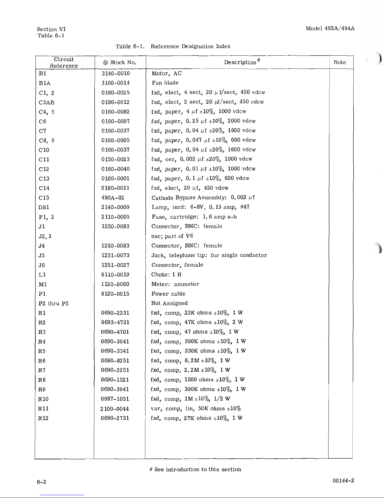
Section
VI
Table
6-1
Table
6-1.
Reference
Designation
Index
Model 492A/494A
Circuit
~
stock
No.
Description
If Note
Reference
B1
3140-0010
Motor,
AC
B1A
3160-0014
Fan
blade
C1, 2
0180-0025
fxd,
elect,4sect,
20
j.L
f/sect,
450 vdcw
C3AB
0180-0012
fxd,
elect,2sect,
20
jJf/sect,
450 vdcw
C4,
5
0160-0082
fxd,
paper,
4
j.Lf
±1O%,
1000 vdcw
C6
0160-0097
fxd,
paper,
0.25
j.Lf
±1O%,
2000 vdcw
C7
0160-0037
fxd,
paper,
0.04
j.Lf
±20%, 1600 vdcw
C8, 9
0160-0005
fxd,
paper,
0.047
j.Lf
±10%, 600 vdcw
C10
0160-0037
fxd,
paper,
0.04
j.Lf
±20%,
1600 vdcw
C11
0150-0023
fxd,
cer,
0.002
j.Lf
±20%, 1000 vdcw
C12
0160-0040
fxd,
paper,
0.01
j.Lf
±1O%,
1000 vdcw
C13
0160-0001
fxd,
paper,
0.1
j.Lf
±10%, 600 vdcw
C14
0180-0011
fxd,
elect,
20
j.Lf,
450 vdcw
C15
490A-82
Cathode
Bypass
Assembly:O.002
j.Lf
DS1
2140-0009
Lamp,
incd: 6-BV,O.15
amp,
#47
F1,
2
2110-0005
Fuse,
cartridge:
1.6
amp
s-b
J1
1250-0083
Connector,
BNC:
female
J2,3
nsr;
part
of V6
J4
1250-0083
Connector,
BNC:
female
J5
1251-0073
Jack,
telephone
tip:
for
single
conductor
J6
1251-0027
Connector,
female
L1
9110-0019
Choke: 1
H
M1
1120-0060
Meter:
ammeter
P1
8120-0015
Power
cable
P2
thru
P5
Not
Assigned
R1
0690-2231
fxd,
comp,
22K
ohms
±10%, 1 W
R2
0693-4731
fxd,
comp,
47K
ohms
±10%, 2 W
R3
0690-4701 fxd,
comp,
47
ohms
±10%, 1 W
R4
0690-3941 fxd,
comp,
390K
ohms
±1O%,
1 W
R5
0690-3341 fxd,
comp,
330K
ohms
±10%, 1 W
R6
0690-8251
fxd,
comp,
8. 2M
±1O%,
1 W
R7
0690-2251
fxd,
comp,2.2M
±1O%,
1 W
R8
0690-1521 fxd,
comp,
1500
ohms
±10%, 1 W
R9
0690-3941
fxd,
comp,
390K
ohms
±10%,
1 W
R10
0687-1051
fxd,
comp,
1M ±10%,
1/2
W
R11 2100-0044
var,
comp,
lin,
50K
ohms
±10%
R12
0690-2731
fxd,
comp,
27K
ohms
±10%, 1 W
# See
introductiontothis
section
6-2
00144-2
Page 37
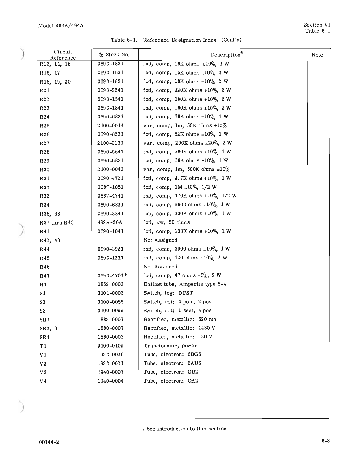
Model 492A/494A
Section
VI
Table
6-1
Table
6-l.
Reference
Designation
Index
(Cont'd)
Circuit
<FiJ
stock
No.
Description*
Note
Reference
R13,14
,
15
0693-1831 fxd
,
comp,
18K
ohms
±10%, 2 W
R16
,
17
0693-1531 fxd,comp,
15K
ohms
±10%, 2 W
R18
,
19
,
20
0693-1831
fxd
,
comp,
18K
ohms
±10%, 2 W
R21
0693-2241
fxd
,
comp,
220K
ohms
±1O%,
2 W
R22
0693-1541 fxd
,
comp,
150K
ohms
±10%, 2 W
R23
0693-1841
fxd
,
comp,
180K
ohms
±1O%,
2 W
R24
0690-6831
fxd
,
comp,
68K
ohms
±10%, 1 W
R25
2100-0044
var1comp,
lin
,
50K
ohms
±10%
R26
0690-8231 fxd
,
comp,
82K
ohms
±10%, 1 W
R27
2100-0133
var1comp,
200K
ohms
±20%, 2 W
R28
0690-5641
fxd
,
comp,
560K
ohms
±1O%,
1 W
R29
0690-6831
fxd
,
comp,
68K
ohms
±10%, 1 W
R30
2100-0043
var1comp,
lin
,
500K
ohms
±10%
R31
0690-4721
fxd
,
comp,
4.7K
ohms
±1O%,
1W
R32
0687-1051
fxd
,
comp,
1M ±10%,
1/2
W
R33
0687-4741 fxd
,
comp,
470K
ohms
±1O%,
1/2
W
R34
0690-6821 fxd,
comp,
6800
ohms
±1O%,
1 W
R35
,
36
0690-3341 fxd,comp,
330K
ohms
±1O%,
1 W
R37
thru
R40
492A-26A fxd,
ww
1 50
ohms
R41
0690-1041 fxd
,
comp,
lOOK
ohms
±10%,
1W
"
R42
,
43
Not
Assigned
R44
0690-3921
fxd
,
comp,
3900
ohms
±10%, 1 W
R45
0693-1211
fxd
,
comp,
120
ohms
±10%, 2 W
R46
Not
Assigned
R47
0693-4701
*
fxd,comp,47ohms
±5%,
2 W
RT1
0852-0003
Ballast
tube,
Amperite
type
6-4
Sl
3101-0003
SWitch,tog:
DPST
S2
3100-0055
SWitch
,
rot:
4
pole
,
2
pos
S3
3100-0099 Switch,rot:
1
sect
,
4
pos
SR1
1882-0007
Rectifier,metallic:
620 rna
SR2
,
3
1880-0007
Rectifier
,
metallic:
1430 V
SR4
1880-0003
Rectifier,metallic:
130 V
T1
9100-0109
Transformer1power
V1
1923-0026
Tube
,
electron:
6BG6
V2
1923-0021
Tube
,
electron:
6AU6
V3
1940-0007
Tube
,
electron:
OB2
V4
1940-0004 Tube
,
electron:
OA2
)
# See
introductiontothis
section
00144-2
6-3
Page 38
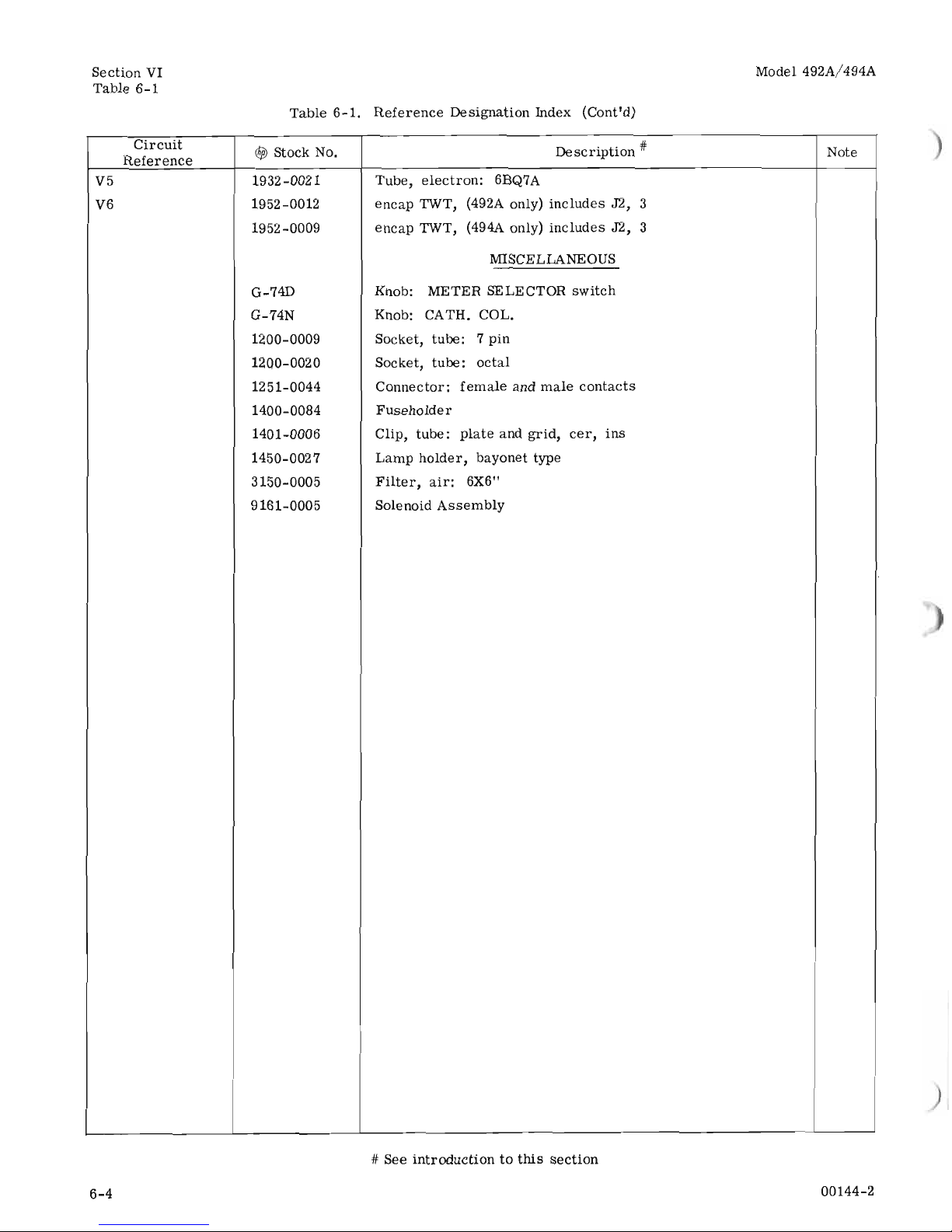
Section
VI
Table
6-1
Table
6-1.
Reference
Designation
Index (Cont'd)
Model 492A/494A
Circuit
r[j>
stock
No.
Description
'if
Note
Reference
V5
1932-0021
Tube,
electron:
6BQ7A
V6
1952-0012
encap
TWT, (492A only)
includes
.12,
3
1952-0009
encap
TWT, (494A only)
includes
.12,
3
MISCELLANEOUS
G-74D
Knob:
METER
SELECTOR
switch
G-74N
Knob: CATH. COL.
1200-0009
Socket, tube:
7
pin
1200-0020
Socket,
tube:
octal
1251-0044
Connector:
female
and
male
contacts
1400-0084
Fuseholder
1401-0006
Clip,
tube:
plate
and
grid,
cer,
ins
1450-0027
Lamp
holder,
bayonet
type
3150-0005
Filter,
air:
6X6"
9161-0005
Solenoid
Assembly
'if
See
introductiontothis
section
6-4
00144-2
Page 39

Model
492A/494A
Table
6-2.
Replaceable
Parts
Section
VI
Table
6-2
)
~stockNo.
Description
#
Mfr.
Mfr.
Part
No.
TQ
RS
490A-82
Cathode
Bypass
Assembly:O.002 Ilf
28480 490A-82
1
1
492A-26A fxd,
WW,
50
ohms
28480 492A-26A
4
1
0150-0023
fxd,
cer,
0.002
Ilf ±20%, 1000 vdcw
91418
JF.002
1 1
0160-0001
fxd,
paper,O.11lf
±1O%,
600 vdcw
56289
160P10496
1 1
0160-0005
fxd,
paper,
0.047
Ilf ±10%, 600 vdcw
56289 160P47390
2
1
0160-0037
fxd,
paper,
0.04
Ilf ±20%, 1600 vdcw
14655
ST16S4-20
2 1
0160-0040
fxd,
paper,O.011lf
±1O%,
1000 vdcw
14655
TST-100
1 1
0160-0082
fxd,
paper,
4 Ilf
±1O%,
1000 vdcw
00656
JP09
2
1
0160-0097
fxd,
paper,
0.25
Ilf ±lO%, 2000 vdcw
00656 2009
1 1
0180-0011
fxd,
elect,
20 Ilf, 450 vdcw
56289
D32550
1 1
0180-0012
fxd,
elect,2sect,
20
Ilf/sect,
450 vdcw
00853
LPI
(obd)
1
1
0180-0025 fxd,
elect,4sect,
20
Ilf/sect,
450 vdcw
56289 D32452
2 1
0687-1051
fxd,
comp,
1M ±10%,
1/2
W
01121
EB-1051
2 1
0687-4741
fxd,
comp,
470K
ohms
±lO%,
1/2
W
01121
EB-4741
1
1
0690-1041
fxd,
comp,
lOOK
ohms
±10%,
1W
01121
GB-1041
1 1
0690-1521
fxd,
comp,
8.2M
±lO%, 1 W
01121
GB-1521
1 1
0690-2231
fxd,
comp,
22K
ohms
±10%, 1 W
01121
GB-2231
1
1
0690-2251
fxd,
comp,
2.2M±10%,
1W
01121
GB-2251
1 1
0690-2731
fxd,
comp,
27K
ohms
±10%, 1 W
01121
GB-2731
1
1
0690-3341
fxd,
comp,
330K
ohms
±lO%, 1 W
01121
GB-3341
3 1
0690-3921
fxd,
comp,
3900
ohms
±1O%,
1 W
01121
GB-3921
1 1
0690-3941
fxd,
comp,
390K
ohms
±lO%, 1 W
01121
GB-3941
2 1
0690-4701
fxd,
comp,47ohms
±10%, 1 W
01121
GB-4701
1
1
0690-4721
fxd,
comp,
4.7K
ohms
±10%, 1 W
01121
GB-4721
1 1
0690-5641
fxd,
comp,
560K
ohms
±1O%,
1 W
01121
GB-5641
1 1
0690-6821
fxd,
comp,
6800
ohms
±1O%,
1 W
01121
GB-6821
1 1
0690-6831
fxd,
comp,
68K
ohms
± 10%, 1 W
01121
GB-6831
2
1
0690-8231
fxd,
comp,
82K
ohms±10%,
1 W
01121
GB-8231
1 1
0690-8251
fxd,
comp,
8.2M
±10%, 1 W
01121
GB-8251
1
1
0693-1211
fxd,
comp,
120
ohms
±10%, 2 W
01121 HB-1211
1
1
0693-1531
fxd,
comp,
15K
ohms
±10%, 2 W
01121 HB-1531
2 1
0693-1541
fxd,
comp,
150K
ohms
±lO%, 2 W
01121
HB-1541
1 1
0693-1831
fxd,
comp,
18K
ohms
±10%, 2 W
01121 HB-1831
6
2
0693-1841
fxd,
comp,
180K
ohms
±lO%, 2 W
01121 HB-1841
1 1
0693-4701~fxd,
comp,47ohms
±5%,
2 W
01121 HB-4701
1
1
0693-4731
fxd,
comp,
47K
ohms
±10%, 2 W
01121 HB-4731
1 1
0852-0003
Tube,
ballast:
Amperite
type
6-4
70563
6-4
1 1
# See
introductiontothis
section
00144-2
6-5
Page 40
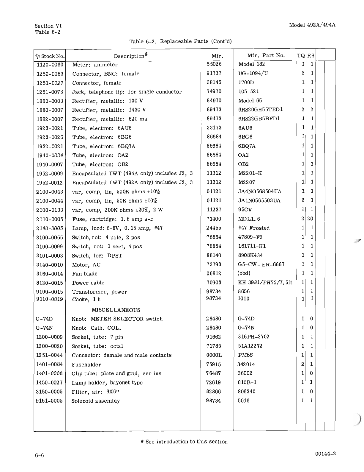
Section
VI
Table
6-2
Table
6-2.
Replaceable
Parts
(Cont'd)
Model 492A/494A
~stockNo.
De
scription
ti
Mfr.
Mfr.
Part
No.
TQ
RS
1120-0060
Meter:
ammeter
55026
Model 182 1 1
1250-0083
Connector,
BNC:
female
91737
UG-1094/U
2
1
1251-0027
Connector,
female
08145 1700D
1
1
1251-0073
Jack,
telephone
tip:
for
single
conductor
74970 105-521
1
1
1880-0003
Rectifier,
metallic:
130 V
84970 Model
65
1 1
1880-0007
Rectifier,
metallic:
1430 V
89473
6RS2OGH55TED1
2 2
1882-0007
Rectifier,
metallic:
620
rna
89473 6RS22GB5BFD1
1
1
1923-0021
Tube,
electron:
6AU6
33173
6AU6
1 1
1923-0026
Tube,
electron:
6BG6
86684 6BG6
1 1
1932-0021
Tube,
electron:
6BQ7A
86684 6BQ7A
1 1
1940-0004
Tube,
electron:
OA2
86684
OA2
1 1
1940-0007
Tube,
electron:
OB2
86684 OB2
1 1
1952-0009
Encapsulated
TWT (494A only)
includes
J2,
3
11312 M2201-K
1 1
1952-0012
Encapsulated
TWT (492A only)
includes
J2,
3 11312 M2207
1
1
2100-0043
var,
comp,
lin,
500K
ohms
±10%
01121 JA4N0568504UA
1 1
2100-0044
var,
comp,
lin,
50K
ohms
±10%
01121
JA1N0565503UA 2
1
2100-0133
var,
comp,
200K
ohms
±20%, 2 W
11237 95CV
1 1
2110-0005
Fuse,
cartridge:
1.6
amp
s-b
71400
MDL1.6
2 20
2140-0005
Lamp,
incd: 6-8V,
0.15
amp,
#47
24455 #47
Frosted
1
1
3100-0055
Switch,
rot:4pole,2pos
76854
47809-F2
1 1
3100-0099
Switch,
rot:
1
sect,4pos
76854 161711-H1
1 1
3101-0003
Switch, tog:
DPST
88140 8908K434
1
1
3140-0010
Motor,
AC
73793
G5-CW-
ER-6667
1 1
3160-0014
Fan
blade
06812
(obd)
1 1
8120-0015
Power
cable
70903
KH
3981/PH70/7.
5ft
1 1
9100-0015
Transformer,
power
98734 8656 1 1
9110-0019
Choke, 1 h
98734
1010
1
1
MISCELLANEOUS
G-74D Knob:
METER SELECTOR
switch
28480
G-74D
1 0
G-74N
Knob:
Cath.
COL.
28480
G-74N
1 0
1200-0009 Socket,
tube:7pin
91662 316PH-3702 1 1
1200-0020
Socket,
tube:
octal
71785 51A12272 1 1
1251-0044
Connector:
female
and
male
contacts
OOOOL
PM6S
1 1
1401-0084
Fuseholder
75915
342014
2
1
1401-0006 Clip tube:
plate
and
grid,
cer
ins
76487 36002
1 0
1450-0027
Lamp
holder,
bayonet
type
72619 81OB-1
1
1
3150-0005
Filter,
air:
6X6"
82866 806340 1 0
9161-0005 Solenoid
assembly
98734 5016
1 1
# See
introductiontothis
section
6-6
00144-2
Page 41

Model
492Aj494A
Appendix
APPENDIX
CODE
LIST
OF
MANUFACTURERS (Sheet 1
of
2)
The following
code
numbers are from
the
Federal Supply
Code
for Manufacturers Cataloging Handbooks
H4-1
(NametoCode)
and H4-2 (Code
to
Name) and their latest supplements. The
date
of revision and
the
dateofthe
supplements used
appear
at
the
bottomofeach
page.
Alphabetical codes have been arbitrarily assignedtosuppliers not appearingintheH4handbooks.
CODE
NO.
MANUFACTURER
ADDRESS
CODE
NO.
MANUFACTURER
ADDRESS
CODE
NO.
MANUFACTURER
ADDRESS
Fullerton,
Calif.
Quincy,
Mass.
Cleveland,
Ohio
Paramus,
N.J.
Precision
Thermometer
and
Inst.
Co.
Philadelphia,
Pa.
Raytheon
Company
Lexington, Mass.
Shallcro..Mfg.
Co.
Selma,
N.C.
Simpson
Electric
Co.
Chicago,
III.
Sonotone
Corp.
Elmsford, N.Y.
Sorenson
& Co., Inc. So. Norwalk,
Conn.
Spaulding
Fibre
Co.,
Inc.
Tonawanda,
N.Y.
Sprague
Electric
Co.
North
Adams,
Mass.
Telex, Inc. St. Paul, Minn.
Union Switch
and
Signal,
Div.
of
Westinghouse
Air Brake
Co.
Swissvale, Pa.
Universal Electric
Co.
Owosso, Mich.
Western
Electric
Co., Inc. New York, N.Y.
Weston
Inst. Diy.ofDaystrom, Inc.
Newark,
N.J.
Wollensak
Optical
Co.
Rochester, N.Y.
Allen Mfg.
Co.
Hartford,
Conn.
Allied
Control
Co.,
Inc. New York, N.Y.
Atlantic
India
Rubber
Works, Inc.
Chicago,
III.
New York, N.Y.
Chicago,
III.
Cleveland,
Ohio
New York, N.Y.
JohnE.Fast&Co.
Dialight
Corp.
General
Ceramics
Corp.
Girard-Hopkins
Drake Mfg.
Co.
Hugh
H. Eby Inc.
Gudeman
Co.
Erie Resistor
Corp.
Hansln
Mfg.
Co.,
Inc.
Helipot
Div.ofBeckman
Instruments,
Inc.
Hughes
Products
Division
of
Hughes
Aircraft
Co.
Newport
Beach,
Calif.
Ampere.
Electronic
Co., Diy.
of
North
Americ"an Phillips
Co.,
Inc.
Hicksville, N.Y.
Bradley
Semicondudor
Corp.
Hamden,
Conn.
Carling
Electric, Inc.
Hartford,
Conn.
GeorgeK.Garre",
Co., Inc.
Philadelphia,
Pa.
Cincinnati,
Ohio
Elyria,
Ohio
San
Jose,
Calif.
Winchester,
Mass.
Fischer
Special
Mfg.
Co.
The
General
Industries
Co.
Jennings
Radio
Mfg.
Co.
J.
H. Winns,
and
Sons
48
6 2 0
49
9 5 6
54294
55026
55933
55938
56t37
562
B9
59446
61775
71218
71
286
71313
70563
70903
70998
71002
71
041
621
1 9
649
5 9
65092
66346
70276
70309
7048
5
71450
71468
71471
71482
71
52
B
7 1 7 B 5
Cinch
Mfg.
Corp.
7 1
984
Dow
Corning
Corp.
72136
Electro
Motive
Mfg.
Co.,
Amperite
Co.,
Inc.
Bolden Mfg.
Co.
Bird
electronic
Corp.
Birnbach
Radio
Co.
80ston
Gear
Works
Diy.
of
Murray Co.ofTexas
Bud
Radio
Inc.
Camloc
Fastener
Corp.
AllenO.Cardwell
Electronic
Prod.
Corp.
Plainville,
Conn.
71
40aBunmann
Fuse Div.ofMcGraw.
Edison Co. St. Louis, Mo.
CTS
Corp.
Elkhart,
Ind.
Cannon
Electric
Co.
Los
Angeles,
Calif.
Cinema
Engineering
Co. Burbank,
Calif.
C.P.Clare&Co.
Chicago,
III.
Standard·Thomson
Corp.,
Clifford
Mfg.
Co.
Div.
Waltham,Ma...
71
590
Centralab
Div.ofGlobe
Union Inc.
Milwaukee, Wis.
71
700
The
Cornish
Wire
Co.
New York, N.Y.
7 1
744
Chicago
Miniature
lamp
Works
Chicago,
III.
7
I
753A.O.
Smith
Corp.,
Crowl~e~;V6range,
N.J.
Chicago,
III.
Midland,
Mich.
Inc.
Willimantic,
Conn.
Chicago,
III.
Brooklyn, N.Y.
Keasbey,
N.J.
Oakland,
Calif.
Chicago,
III.
Philadelphia,
Pa.
Chicago,
III.
Erie, Pa.
Princeton,
Ind.
73
29
3
73
445
73
5 0 6
73
5 5 9
73
6B 2
73743
73793
73905
7445
5
723
5 4
72
619
72656
72758
72765
72B25
729
2 8
72982
73
0
61
73138
Teterboro,
N.J.
General
Electric
Co.
G.E.,
Lamp
Division
Nela
Park,
Cleveland,
Ohio
General
Radio
Co.
Wist
Concord,
Mass.
Grobet
File
Co.ofAmerica,
Inc.
Carlstadt,
N.J.
Hamilton
Watch
Co.
Lancaster,
Pa.
Hewlett-Packard
Co.
Palo
Alto,
Calif.
G.E.
Rlceivin9
Tube
Dept.
Owensboro,
Ky.
lectrohm
Inc.
Chicago,
III.
P.R.Mallory&Co.,
Inc.
Indianapolis,
Ind.
Mechanical
Industries
Prod.
Co.
Akron,
Ohio
Miniature
Precision Bearings, Inc.
Keone,
N.H.
Chicago,
III.
Englewood,
Colo.
Skokie, III.
Cambridge,
Mass.
Muter
Co.
C.A.Norgren
Co.
Ohmite
Mfg.
Co.
Polaroid
Corp.
09026
091
34
09250
09569
40920
10411
10646
11236
11237
24446
24455
1171
7
1 1
870
12697
146
5 5
a7 1
17
Transistor Electronics
Corp.
Minneapolis,
Minn.
07138
Westinghouse
Electric
Corp.
Electronic
Tube
Div. Elmira, N.Y.
07261Avnet
Corp.
Los
Angeles,
Calif.
a7 2
'3
Fairchild
Semiconductor
Corp.
Mountain
View,
Calif.
a7 9 1 a
Continental
Device
Corp.
Hawthorne,
Calif.
a7 9 1 3
Rhelm
Semiconductor
Corp.
Mountain
View,
Calif.
07980
Boonton
Radio
Corp.
800nton,
N.J.
08145
U.S.
Engineering
Co.
los
Angeles,
Calif.
083
5 B Burge..Battery
Co.
Niagara
Falls,
Ontario,
Canada
oB
717Sloan
Company
Burbank,
Calif.
08718Cannon
Electric
Co.
Phoenix Div. Phoenix,
Aril.
a8 7 9 2 CBS
Electronics
Semiconductor
Operations,
Div.ofC.B.S. Inc.
Lowell, Mass.
Babcock
Relays, Inc.
Costa
Mesa,
Calif.
Texas
Capacitor
Co.
Houston,
Texas
Electro
Assemblils,
Inc.
Chicago,
Ill.
M~~o::d~~tt.~J:
CO'T:~onto,
Ontario,
Canada
Ti·Tal, Inc. Berkeley,
Calif.
Carborundum
Co.
Niagara
Falls, N.Y.
CTS
of
Borne, Inc. Berne,
Ind.
Chica90
TelephoneofCalifornia,
Inc.
So.
Pasadena,
Calif.
1 1312
Microwave
Electronics
Corp.
Palo
Alto,
Calif.
1 1
71
1
General
Instrument
Corporation
Semiconductor
Division Newark,
N.J.
Imperial
Electronics, Inc. Buena Park,
Calif.
Melabs,
Inc. Palo
Alia,
Calif.
Clarostat
Mfg.
Co.
Dover,
N.H.
Cornell
Dubilier
Elec.
Corp.
So.
Plainfield,
N.J.
1
5909
The Daven
Co.
livingston,
N.J.
1
675
B Delco
Radio
Div.ofG.M.Corp.
Kokomo, Ind.
1 8 B7 3
E.
I. DuPont
and
Co.,
Inc.
Wilmington,
Del.
1
931
5 Eclipse
Pioneer,
Div.
of
Bendix
Aviation
Corp.
I
9500
Thomas A. Edison Industries,
Div.
of
McGraw-Edison
Co.
West
Orange,
N.J.
Electra
Manufacturing
Co.
Kansas
City,
Mo.
Electronic
Tube
Corp.
Philadelphia,
Pa.
Fanst.el
Metallurgical
Corp.
No.
Chicago,
III.
2 1
335
The Fafnir Bearing
Co.
New Britain,
Conn.
21
964
Fed.
Telephone
and
Radio
Corp.
Clifton,
N.J.
Schenectady,
N.Y.
19701
201
83
21
520
246
5 5
26462
26992
2848
0
131
73
35
4 3 4
37942
39
5
43
421
90
439
9 0
446
5 5
47904
Colton,
Calif.
New York, N.Y.
Culver
City,
Calif.
Northlake,
III.
Chicago,
III.
Humidial
Co.
Westrex Corp.
Garlock
Packing
Co.,
Electronic
Products
Div.
Camden.
N.J.
A.rovol
Corp. New Bedford,
Man.
Amp,
Inc.
Harrisburg,
P,.
Aircraft
Radio
Corp.
Boonton,
N.J.
S.ng.mo
Electric Company,
Ordill
Division
(Capacitors)
Marion,
III.
Go.
Engine.ring
Co.
Los
AnQlles,
Calif.
CarlE.Holmes
Corp.
los
Angeles,
Calif.
Allen Bradley
Co.
Milwaukee,
Wis.
Litton Industries, Inc. Beverly Hills,
Calif.
Pacific
Semiconductors,
Inc.
Culver
City,
Calif.
Radio
Corp.
of America
Semiconductor
and
Materials
Div.
Somerville,
N.J.
Vocaline
Co.
of
America,
Inc.
Old
Saybrook,
Conn.
Hopkins
Engineerin9
Co.
San
Fernando,
Calif.
G.E.
Semiconductor
Products
Dept.
Syracuse, N.Y.
Apex
Machine
& Tool
Co.
Dayton,
Ohio
Eldema
Corp.
EI
Monte,
Calif.
Transitron
Electronic
Corp.
Wakefield,
Mass.
Pyrofilm Resistor
Co. Morristown,
N.J.
Air
Marine
Motors,
Inc. Los
Angeles,
Calif.
Arrow,
Hart
and
Hegeman
Elect.
Co.
Hartford,
Conn.
Elm.nco
Products
Co.
New York, N.Y.
Hi-Q
DivisionofAerovox Myrtle Boach, S.C.
Eltl:c~r~t~icnsaID~is~~~
Co.,
Burbank,
Calif.
Dymec Division
of
Hewlett-Packard
Co.
Palo
Alto,
Calif.
Sylvania Electric Prods., Inc.
Electronic
Tube
Div.
Mountain
View,
Calif.
Motorola,
Inc.,
Semiconductor
Prod. Div. Phoenix,
Arilona
Filtron
Co.,
Inc.
Western
Division
Automatic
Electric
Co.
PM
Motor
Co.
Twentieth
Century
Plastics, Inc.
Los
Angeles,
Calif.
Westinghouse
Electric
Corp.,
Semi·Cbnductor
Dept.
Youn9wood,
Pa.
Illumitronic
Engineering
Co.
Sunnyvale,
Calif.
Barber
Colman
Co.
Rockford, III.
Metropolitan
Telecommunications
Corp.,
Metro
Cap.
Di..
Brooklyn, N.Y.
Stewart
Engineerin9
Co.
Santa
CruI,
Calif.
TheBa..
ick
Co.
Bridgeport,
Conn.
Beede
Electrical
Instrument
Co., Inc.
Penacook,
N.H.
Torrington
Mfg. Co.,
West
Div.
Van Nuys,
Calif.
00656
00779
00781
00853
00334
00335
00373
00866
00891
01121
01255
01
281
02735
02771
02777
04404
04651
0471
3
01295
Texas
Instruments,
Inc.
Transistor Products
Diy.
Dallas,
Tu.s
01
349
The
Alliance
Mfg.
Co.
Alliance,
Ohio
01
561
Cha..i-Trak
Corp.
Indianapolis,
Ind.
01
589
Pacific
Relays, Inc. Van Nuys,
Calif.
o1
930
Amerock
Corp.
Rockford, III.
019'
1 Pulse
Engine.ring
Co. Santa
Clara,
Calif.
021,..
Ferrolcub.
Corp.
of
America
Saugerties,
N.Y.
022B6Cole
Mfg.
Co.
Palo
Alia,
Calif.
02660
Amphenol·Borg
Electronics
Corp.
Chicago,
III.
047
73
048
7 0
05006
05277
05624
05729
05783
06004
06555
06812
03508
03705
03797
038
7 7
038
8 8
039
5 4
04009
04062
042
2 2
0429
8
05593
047
3 2
071
1 5
Corning
Glass
Works
Electronic
Components
Oept.
Bradford,
Pa.
Paudena,
Calif.
o7 1 2 6
Digitran
Co.
)
)
00015·19
Reviled:,December
1961
From:
F.S.C.
Handbook Supplements
H4-1
Dated October
1961
H4-2
Dated November
1961
00144-2
i-I
Page 42

Appendix
Model
492A/494A
APPENDIX
CODE
LIST
OF MANUFACTURERS (Sheet 2
of
2)
CODE
NO.
MANUFACTURER
ADDRESS
CODE
NO.
MANUFACTURER
ADDRESS
CODE
NO.
MANUFACTURER
ADDRESS
Attleboro,
Mass.
Madison,
Wis.
Evanston, III.
Yonkers, N.Y.
New York, N.Y.
Waltham,
Mass.
Versailles,
Ky.
Providence,
R.1.
Palo
Alto,
Calif.
Mineola,
N.Y.
Burbank,
Calif.
New York, N.Y.
Palo
Alto,
Calif.
Chicago,
III.
Chicago,
III.
Sunnyvale,
Calif.
Olean,
N.Y.
Mt.
Carmel,
III.
los
Angeles,
Calif.
Chicago,
III.
Burlington, Mass.
Oakland,
Calif.
Danvers,
Mass.
Jamaica,
N.Y.
Pasadena,
Calif.
So.
Pasadena,
Calif.
Mamaroneck,
N.Y.
Redwood
City,
Calif.
Methode
Mfg.
Co.
Weckesser
Co.
Huggins
laboratories
Hi-Q
DivisionofAerovox
Thordarson-Meissner
Div.
of
Maguire
Industri-.s. Inc.
Solar
Manufacturing
Co.
Carlton
Screw
Co.
Microwave
Associates,
Inc.
Excel
Transformer
Co.
Automatic
and
Precision
Mfg.
Co.
CBS
Electronics,
Div. of C.B.S., Inc.
Axel Brothers Inc.
Francis
l.
Mosley
Microdot,
Inc.
Sealectro
Corp.
Carad
Corp.
Palo
Alto
Engineering
Co.,
Inc.
North
Hills
Electric
Co.
Clevite
Transistor
Prod.
Div.ofClevite
Corp.
International
Electronic
Research
Corp.
Columbia
Technical
Corp.
Varian
Associates
Marshall
Industries,
Electron
Products
Division
Pasadena,
Calif.
Control
Switch Division,
Controls
Co.
of
America
EI
Segundo,
Calif.
Delevan
Electronics
Corp.
East
Aurora,
N.Y.
Wileo
Corporation
Indianapolis,
Ind.
Renbrandt,
Inc. Boston, Mass.
Hoffman
Semiconductor
Div.
of
Hoffman
Electronics
Corp.
Technology
Instrument
Corp.
of
Calif.
Newbury
Park,
Calif.
96296
96
3 3 0
96341
96
5 0 1
97539
981
41
98220
98278
98291
98405
98734
95354
95987
96
0 6 7
96
0 9 5
96
2
56
97966
98821
98925
98978
99109
99
3 1 3
99
515
99
9 5 7
99
7 0 7
99
8 0 0
99848
99
9
34
99942
0000
N
OOOOP
OOOOT
THE
FOLLOWING
H·P
VENDORS HAVENONUM.
BER
ASSIGNEDINTHE
LATEST
SUPPLEMENT TO
THE FEDERAL SUPPLY
CODE
FOR MANUFACTURERS
HANDBOOK.
0000FMalco
Tool
and
Die Los
Angeles,
Calif.
a a a a J Telefunken
(c/o
American
Elite)
a a a a L
Winchester
Electronics,
Inc.
Santa
Monica,
Calif.
a a a a M
Western
Coil
Div.ofAutomatic
Ind.,
Inc.
Redwood
City,
Calif.
Nahm-Bros.
Spring
Co.
San
leandro,
Calif.
Ty·Car
Mfg.
Co.,
Inc.
Holliston,
Mass.
Texas
Instruments,
Inc.
Metals
and
Controls
Div.
0000
U Tower
Mfg.
Corp.
a a a a W
Webster
Electronics
Co.
Inc.
Now York, N.Y.
a a a 0 X
Spruce
Pine
Mica
Co.
Spruce
Pine,
N.C.
0000YMidland
Mfg.
Co.
Inc. Kansas
City,
Kans.
0000ZWillow
Leather
Products
Corp.
Newark,
N.J.
000
A A 8ritish
Radio
Electronics
Ltd.
Washington,
D.C.
oa a B B Precision
Instrument
Components
Co.
Van Nuys,
Calif.
000
C C
Computor
Diodo
Corp.
Lodi,
N.J.
a 0
aDD
General
Transistor
los
Angeles,
Calif.
a a 0 E EA.Williams
Manufacturing
Co.
San
Jose,
Calif.
a a a F F
Carmichael
Corrugated
Specialties
Richmond,
Calif.
a a a G G
Soshen
Die
Cutting
Service
Goshen,
Ind.
Plainfield,
N.J.
Loveland,
Colo.
Newark,
N.J.
Huntington,
Ind.
Festus, Mo.
New York, N.Y.
Rotron
Manufacturing
Co.,
Inc.
Woodstock,
N.Y.
Glendale,
Calif.
Cambridge,
Mass.
Darlington,
S.C.
Los
Angeles,
Calif.
Union,
N.J.
Red Bank,
N.J.
8rooklyn, N.Y.
Vector
Electronic
Co.
Carr
Fastener
Co.
Pyramid
Electric
Co.
Electro
Cords
Co.
Victory
Engineering
Corp.
Bendix
Corp.,
Red Bank Div.
Smith,
Herman
H., Inc.
Gavitt
Wire
and
Cable
Co.,
Div.ofAmerace
Corp.
Brookfield, Mass.
Burroughs
Corp.,
Electronic
Tube
Div.
Model
Eng.
and
Mfg.,
Inc.
Loyd
Scruggs
Co.
Arco
Electronics,
Inc.
A.
J.
Glesener
Co.,
Inc.
San
Francisco,
Calif.
Good
All
Electric
Mfg.
Co.
Ogallala,
Neb.
Sarkes
Tanian,
Inc.
Bloomington,
Ind.
Boonton
Molding
Company
Boonton,
N.J.
R.M.Bracamonte&Co.
San
Francisco,
Calif.
New
Haven,
Conn.
Chicago,
III.
Tung-Sol
Electric,
Inc.
Curtiss-Wright
Corp.,
Electronics
Div. East
Paterson,
N.J.
Tru
Ohm
Prod.
Div.ofModel
Engineering
and
Mfg.
Co.
Chicago,
111.
Worcester
Pressed
Aluminum
Corp.
Worcester,
Mass.
Miami,
Fla.
Woodside,
N.Y.
New York, N.Y.
Burbank,
Calif.
Sheridan,
Wyo.
Bridgeport,
Conn.
United
Transformer
Co.
U.S.
Rubber
Co.,
Mechanical
Goods
Div.
Passaic,
N.J.
Bearing
Engineering
Co.
San
Francisco,
Calif.
Connor
Spring
Mfg.
Co.
San
Francisco,
Calif.
Radio
Materials
Co.
Chicago,
Ill.
Augat
Brothers,'lnc.
Attleboro,
Mass.
Dale
Electronics,
Inc.
Columbus,
Nebr.
Elco
Corp.
Philadelphia,
Pa.
Gremar
Mfg.
Co.,
Inc.
Wakefield,
Mass.
K F
Development
Co.
Redwood
City,
Calif.
Minneapolis-Honeywell
Regulator
Co.,
Micro-Switch Division
Freeport,
III.
Universal
Metal
Products,
Inc.
Bassett Puente,
Calif.
Sylvania
Electric
Prod.
Inc.,
Semiconductor
Div.
Woburn,
Mass.
Robbins
and
Myers, Inc. New York, N.Y.
Stevens
Mfg.
Co.,
Inc.
Mansfield,
Ohio
lnsuline-Van
Norman
Ind.,
Inc.
Electronic
Division
Manchester,
N.H.
Raytheon
Mfg.
Co.,
Industrial
Components
Div.,
Receiving
Tube
Operation
Quincy,
Mass.
Raytheon
Mfg.
Co.,
Semiconductor
Div.,
California
Street
Plant
Newton,
Mass.
Scientific
Radio
Products,
Inc
Allies
Products
Corp.
Continental
Connedor
Corp.
Leecraft
Mfg.
Co.,
Inc.
Lerco
Electronics,
Inc.
National
Coil
Co.
Vitramon,
Inc.
82877
83594
82893
83058
83125
831
48
831
86
83298
83330
83501
83777
83821
841
71
84396
84411
84970
85454
85474
85660
8591
1
866
8 4
89665
90179
Koiled
Kords, Inc.
Seamless
Rubber
Co.
Radio
Corp.ofAmerica,
RCA
Electron
Tube
Div.
Harrison,
N.J.
8721
6 PhilcoCorp.
(Lansdalo
Division)
Lansdale,
Pa.
a
7473
Western
Fibrous
Glass
Products
Co.
San
Francisco,
Calif.
aa1 4 a
Cutler-Hammer,
Inc. Lincoln, III.
a9 4 7 3
General
Electric
Distributing
Corp.
Schenectady,
N.Y.
a9
/)3/)
Carter
Parts
Div.ofEconomy Baler
Co.
Chicago,
III.
Chicago,
III.
94144
94145
933
3 2
92196
9097
0
91260
91
41
8
91
506
91
637
91662
91737
91
827
91921
93369
9341
0
93983
94148
9431
0
941
54
941
97
946
8 2
95236
95238
9 S
26
3
95264
95265
95275
Newton,
Mass.
Du
Bois, Pa.
Clifton,
N.J.
Greenwich,
Conn.
Emporium,
Pa.
East
Newark,
N.J.
Chicago,
III.
Div.
of
Columbus
16,
Ohio
Defiance,
Ohio
Now York, N.Y.
Boston, Mass.
Wallingford,
Conn.
Chicago,
III.
Riverside,
Calif.
Industrial
Condenser
Corp.
Chicago. III.
R.F.
Products
DivisionofAmphenol-
Borg
Electronics
Corp.
Danbury,
Conn.
E.F.Johnson
Co.
Waseca,
Minn.
Int.rnational
Resistance
Co.
Philadelphia,
Pa.
Jones,
Howard
B.,
Division
of
Cinch
Mfg.
Corp.
James
Knights
Co.
Kulka Electric
Corporation
lent
Electric
Mftll.
Co.
litt.lfuse
Inc.
Lord
Mfg.
Co.
C.W.Marwedel
Micamold
Electronic
Chicago,
III.
Sandwich,
III.
Mt.
Vernon, N.Y.
Chicago,
III.
Des Plaines, Ill.
Erie, Pa.
San
Francisco,
Calif.
Mfg.
Corp.
8rooklyn, N.Y.
James
Millen
Mfg.
Co.,
Inc.
Malden,
Mass.
J.W.Miller
Co.
Los
Angeles,
Calif.
Monadnock
Mills San
Leandro,
Calif.
Mueller
Electric
Co,
Cleveland,
Ohio
Oak
Manufacturing
Co.
Chicago,
III.
Sendix Pacific Division
of
8endix
Corp.
No.
Hollywood,
Calif.
Phaostron
Instrument
and
Electronic
Co.
South
Pasadena,
Calif.
Pott.r
and
Brumfield, Div.ofAmerican
Machine
and
Foundry
Princeton,
Ind.
Radio
Condenser
Co.
Camden,
N.J.
Radio
Receptor
Co.,
Inc. Brooklyn, N.Y.
Resistance
Products
Co.
Harrisburg,
Pa.
Signal
Indicator
Corp.
New York, N.Y.
Tilley
Mfg.
Co.
San
Francisco,
Calif.
Stackpole
Carbon
Co.
St.
Marys, Pa.
Tinnerman
Products,
Inc.
Cleveland,
Ohio
Transformer
Engineers
Pasadena,
Calif.
Ucinite
Co.
Newtonville,
Mass.
Veeder
Root, Inc.
HarHord,
Conn.
Wenco
Mfg.
Co.
Chicago,
III.
Continental-Wirt
Electronics
Corp.
Philadelphia,
Pa.
New
Rochelle,
N.Y.
Zierick
Mfg.
Corp.
Mepco
Division
of
Sessions
Clock
Co.
Morristown,
N.J.
Times
Facsimile
Corp.
New
York, N.Y.
Electronk
Industries
Association
Any
brand
tub.
meeting
EIA
standards
Washington,
D.C.
Unimu
Switch, Div.
of
W.L.Maxson
Corp.
Oxford
Electric
Corp.
Bourns
Laboratories,
Inc.
Aero
Div.ofRobertshaw
Fulton
Controls
Co.
All
Star
Products
Inc.
Hammerlund
Co.,
Inc.
Stevens,
Arnold,
Co.,
Inc.
International
Instruments,
Inc.
New
Haven,
Conn.
Wilkor
Products,
Inc.
Cleveland,
Ohio
Raytheon
Mfg.
Co.,
Industrial
Components
Div.,
Industr.
Tube
Operations
International
Rectifier
Corp.
EI
Segundo,
Calif.
Watertown,
Mass.
Skokie, III.
Barry
Controls,
Inc.
Carter
Parts
Co.
Jeffers
Electronics
Division
of
Speer
Carbon
Co.
AllenB.DuMont
Labs.,
Inc.
Maguire
Industries,
Inc.
Sylvania
Electric
Prod.
Inc.,
Electronic
Tube
Div.
Astron
Co.
Switchcraft,
Inc.
Metals
and
Controls,
Inc.,
Texas
Instruments,
Inc.,
Spencer
Prods.
Research
Products
Corp.
76
48
7
16493
76
5 3 0
76545
76854
77068
75378
75382
7581
8
7591
5
76
0 0 5
76
210
76433
77221
80207
77
6 3 0
776
3 8
77764
78
2 8 3
78471
78488
78553
78790
78947
79142
79251
79727
7996
3
80031
77
3 4 2
748
6 1
74868
749
7 0
75042
75173
81
483
80248
80294
8041
1
80486
80583
80640
81
030
81
41
5
81453
81860
82042
82142
821
70
82209
8221
9
82376
82389
82647
82866
801
30
801
31
00015-19
Revised:
/)
December
1961
From:
F.S,C,
Handboo~
Supplements
H4-1
Dated
October
1961
H4-2
Dated
November
1961
i-2
00144-2
Page 43

(ffj)
M.ANUAL
CHANGES
MODEL
492A/494A
TRAVELIl\G-WAVE
AMPLIFIER
M1\nual
Serial
Prefixed:
010-
Manual
Printed:
1/62
To
adapt
this
manuaitoinstruments
with
other
serial
prefixes
check
for
errata
below, and
make
changes
shown in
tables.
Instrument
Serial
Prefix'
ALL
Make
Manual
Changes
ERRATA
Instrument
Serial
Prefix
Make
Manual
Changes
492A
•••••••
O. 5
rna
494A
•••••••
1.0
rna
-
ERRATA:
'/a/63
Table
6-1.
SRI:
Change
to
rectifier.
metallic:
65
rna,
l;OV;
~Stock
No.
1880-0003.
SR4:
Change
to
rectifier.
metallic:
620
rna.
l30V;
!tStock
No.
1882-0007.
Page
3-1,'
Table
3-1.
'.
Change
HELIX
CU~RENT
to
read:
Table
6-1.
VI:
Change
descrip:ion
to
"tube.
clectro:l:
6BG6G".
Table
6-2.
'iStock
~o.
0690-1521:
Change
description
to
"fxd.
comp.1500
ohm.,
±.IO';'o.
1
W".
1j'Stock
No.
1923-0026:
Change
description
to
"tube.
electron:
6BG6G".
Under
lo-tlSCELLA1\"EOUS,
change
~Stock
1\"0.
1401-0084
to
1400-0084.
Section
V,
Paragraph
5-2ge.
Line3sh",uirl
read
33
folio'."3:
"~rc
t~r
thon
-0
m·.·
...
Table
I-I.
Specifications,
Hum
a:1d
SpUrim.l3
~lcdulation:
Char:geto"At
least
40db
below
signal
le';el"
forr"xlel
492A
and
494A.
S
:??:e':lle
.:
;.~
f::;r
-i
Q
2h,'
~').;;...
-~.-
Page 44

•
PRINTED
IN
U.S.A.
 Loading...