

VHF OSCILLATOR 3200B
ranted springs detects ranted springs detects range for one year in range concentration
BOUATR
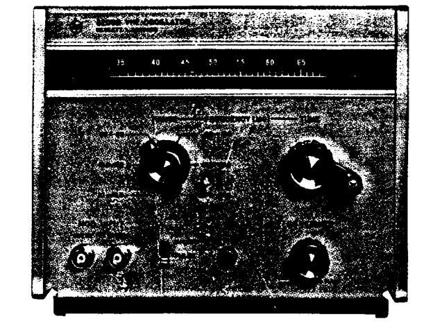

TABLE OF CONTENTS
| - | ||
|---|---|---|
| De | ana | |
| LEC |
Section
| Ī | GEN | ERAL INFORMATION | ||
|---|---|---|---|---|
| _ | 1-1 | Introduction | 1-1 | |
| 1-5 | Supplementary Equipment. | 1-1 | ||
| 1-7 | Instrument Identification | 1-1 | ||
| v | ||||
| II | INST. | ALLATION | ||
| 2-1 | Initial Inspection | 2-1 | ||
| 2-5 | Preparation for Use | 2-1 | ||
| 2-6 | Power Requirements | 2-1 | ||
| 2-8 | 115/230 Volt Operation | 2-1 | ||
| 2-11 | Power Cable. | 2-1 | ||
| 2-14 | Ventilation | 2-1 | ||
| 2-16 | Installation | 2-1 | ||
| 2-18 | Repackaging for Shipment | 2-1 | ||
| ODET | ||||
| ш | OPEr | 0.1 | ||
| 3-1 | 3-1 | |||
| 3-3 | Operating Controls | 3-1 | ||
| 3-5 | Operating Instructions | 3-1 | ||
| 3-6 | General | 3-1 | ||
| 3-8 | Turn-On Procedure | 3-1 | ||
| 3-10 | Using the Output Attenuator | 3-1 | ||
| 3-12 | Modulation Inputs | 3-1 | ||
| 3-17 | Operational Guide | 3-3 | ||
| 3-19 | Output Level | 3-3 | ||
| 3-21 | RF Distortion | 3-3 | ||
| 3-23 | Typical Drift | 3-4 | ||
| 3-25 | Frequency Response | - | ||
| (Modulation) | 3-4 | VI | ||
| 3-27 | Amplitude Modulation | 3-5 | ||
| IV | PRIN | CIPLES OF OPERATION |
4-1 General . 4-1 4-3 RF Oscillator . 4-1
| 4 | 4-6 | Attenuator | 4-1 |
|---|---|---|---|
| 1- 8 | Modulation | 4-1 | |
| 4 | 4–14 | External B+ Operation | 4-2 |
| - | MATN | TENANCE | |
| 5-1 | Introduction | 5-1 | |
| 5-3 | Lubrication | 5-1 | |
| ļ | 5-5 | Test Equipment Required | 5-1 |
| 5-7 | Performance Checks | 5-1 | |
| 5-9 | RF Range and Accuracy. | 5-1 | |
| 5-11 | RF Stability | 5-1 | |
| Ę | 5-13 | RF Output | 5-2 |
| Ę | 5-15 | AM Range and Distortion | 5-3 |
| Ę | 5-17 | External PM Requirements. | 5-3 |
| Ę | 5-19 | Troubleshooting and Repair | 5-4 |
| 5 | 5-20 | Troubleshooting Chart | 5-4 |
| Ę | i-22 | Tube and Semiconductor | |
| Replacement | 5-4 | ||
| 5 | -24 | Transistor Insulators | 5-4 |
| 5 | -26 | Voltages | 5-4 |
| 5 | -28 | Mechanical Disassembly | |
| Procedures | 5-5 | ||
| 5 | -29 | Cover Removal | 5-5 |
| 5 | -32 | Troubleshooting and Repair | |
| Setup | 5-5 | ||
| 5 | -35 | Front Panel Disassembly | 5-5 |
| 5 | -37 | Turret Assembly Removal | 5-6 |
| 5 | -39 | Dial Stringing Procedure | 5-6 |
| 5 | -41 | Adjustment and Calibration | 5-6 |
| Ī | REPL | ACEABLE PARTS | |
| Ē | 5-1 | Introduction | 6-1 |
| 5-1 | Introduction | • | ٠ | • | ٠ | 6-1 |
|---|---|---|---|---|---|---|
| 6-3 | Ordering Information. | 6-1 |
VII SCHEMATIC DIAGRAMS
7-1 Introduction....
009363
LIST OF ILLUSTRATIONS
| Number | Page | |
|---|---|---|
| 1-1 | Model 3200B VHF Oscillator | 1-1 |
| 3-1 | 3200B Operating Controls | 3-2 |
| 3-2 | Typical Maximum Power Output. | 3-3 |
| 3-3 | Typical RF Output Waveforms. | 3-3 |
| 3-4 | Typical Frequency Drift | 3_4 |
| 3-5 | Typical Frequency Response. | 3-4 |
| 4-1 | Block Diagram, 3200B | 4-0 |
| 4-2 | RF Oscillator Circuits. | 4-0 |
| 4-3 | Amplitude Modulation, 3200B | 4_0 |
| 4-4 | Pulse Modulation, 3200B. | 4_1 |
| 4-5 | External B+ Operation | 4-9 |
| 4-6 | Power Supply, 3200B | 4-2 |
| 5-1 | AM Characteristics Setup | 5_9 |
| 5-2 | AM Characteristics. Oscilloscope Displays | 5-2 |
| 5-3 | PM Requirements Setun | 5 9 |
| 5-4 | Troubleshooting Tree - Power Output |
0-0
5 4 |
| 5-5 | Troubleshooting and Rengin Setup | 5-4 |
| 5-6 | Dial Stringing | 5-5 |
| 5-7 | RF Calibration Setup | 5-6 |
| 5-8 | ||
| 6-1 | General Arrangement | 6-4 |
| 6-2 | Cabinet Parts. | 6-5 |
| 6-3 | Front Section and Panel Assembly. | 6-7 |
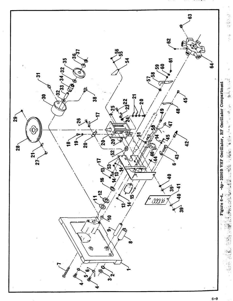
| 6-4 | RF Oscillator Compartment | 6_0 |
| 6-5 | Rear Section and RF Compartment Cover | 6-11 |
| 7-1 | Schematic Diagram | 7-1 |
LIST OF TABLES
| 1-1 | Specifications | 1-0 |
|---|---|---|
|
5-1
5-2 |
Test Equipment Recommended |
5-2
5-2 |
| 6-1 | Reference Designator Index | 6-2 |
| 7-1 | Schematic Diagram Notes | 7-1 |
Table 1-1. Specifications
- Frequency range: 10 to 500 MHz in six bands: 10 to 18.8 MHz; 18.5 to 35 MHz; 35 to 68 MHz; 68 to 130 MHz; 130 to 260 MHz; 260 to 500 MHz.
- Frequency accuracy: within ±2% after 1/2 hour warmup
Frequency calibration: increments of less than 4%.
Frequency stability (after 4-hour warmup under 0.2 mw load): short term (5 minutes) ±0.002%; long term (1 hour) ±0.02%; line voltage (5-volt change) ±0.001%.
RF output:
- Maximum power (across 50-ohm external load): >200 mw (10 to 130 MHz); >150 mw (130 to 260 MHz); >25 mw (260 to 500 MHz).
- Range: 0 to >120 db attenuation from maximum output
Load impedance: 50 ohms nominal.
RF leakage: sufficiently low to permit measurements at 1 µv. RFI: meets requirements of MIL-I-6181D.
Amplitude modulation: externally modulated.
Range: 0 to 30%.
Distortion: <1% at 30% AM.
External requirements: approximately 20 volts rms into 600 ohms for 30% AM, 200 Hz to 100 kHz.
Pulse modulation: externally modulated.
External requirements: 2.5 volt negative pulse into 2000 ohms.
Power: 105 to 125 v or 210 to 250 v, 50 to 1000 Hz, 30 w.
Weight: net 15 lbs. (6.8 kg), shipping 19 lbs. (8.6 kg).
Accessories available: 13515A Frequency Doubler Probe: 00501B, 00514B, 00517B Output Cables; 00502B, 00506B Patching Cables.
SECTION I GENERAL INFORMATION
1-1. INTRODUCTION
1-2. The 3200B VHF Oscillator is designed for general purpose laboratory use in the frequency range of 10 to 500 MHz. Typical applications include: receiver and amplifier testing; driving bridges, slotted lines, antenna and filter networks; and use as a local oscillator for heterodyne detector systems. It is completely self-contained and housed in a modular cabinet which can be adapted for standard rack mounting.
1-3. A push-pull oscillator is housed in a rugged aluminim casting for maximum stability and extremely low leakage. Six frequency ranges are provided for adequate bandspread on the slide-rule dial. Amplitude and pulse modulation may be obtained by the use of suitable external sources. The RF output is coupled through a waveguide-belowcutoff variable attenuator. An electronic RF level vernier is included as a front panel control.
1-4. A solid-state power supply furnishes all necessary operating voltages, including dc to the os-
cillator tube heaters for minimum hum modulation and maximum tube life.
1-5. SUPPLEMENTARY EQUIPMENT
1-6. The -hp- 13515A Frequency Doubler Probe extends the frequency range of the 3200B up to 1000 MHz. In the frequency range from 500 to 1000 MHz, the power output will be in excess of 4 mW across an external 50 ohm load.
1-7. INSTRUMENT IDENTIFICATION
1-8. Hewlett-Packard uses a two-section, eightdigit serial number (on instrument rear panel) to identify instruments (000-00000). The first three digits are a serial prefix number, and the last five digits refer to a specific instrument. If the serial prefix on your instrument does not appear on the title page of this manual, there are differences between the manual and your instrument which are described in the Appendix or in a Manual Change Sheet included with the manual. If the change sheet is missing, the information can be supplied by your local sales office.
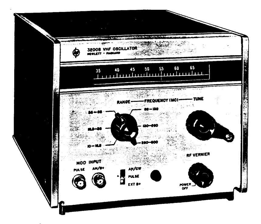
Figure 1-1. Model 3200B VHF Oscillator
SECTION II INSTALLATION
2-1. INITIAL INSPECTION.
2-2. MECHANICAL CHECK. If damage to the shipping carton is evident, ask that the carrier's agent be present when the instrument is unpacked. Inspect the instrument for scratches, dents, broken knobs and switches, and any other mechanical damage. Also check the cushioning material for signs of severe stress as an indication of rough handling in transit.
2-3. PERFORMANCE CHECK. The electrical performance of the 3200B should be verified as soon as possible after receipt. A performance check that is suitable for initial inspection is contained in Section V.
2-4. CLAIM FOR DAMAGE. If upon receipt, the 3200B is damaged or fails to meet performance specifications, notify the carrier and the nearest Hewlett-Packard Sales and Service Office immediately (A list of offices is provided at the back of this manual). Retain the shipping carton and padding material for the carrier's inspection. The sales and service office will arrange for the repair or replacement of the instrument without waiting for the claim against the carrier to be settled.
2-5. PREPARATION FOR USE.
2-6. POWER REQUIREMENTS.
2-7. The 3200B requires a power source of 105 to 125 V or 210 to 250 V, 50 to 1000 Hz, which can supply approximately 30 watts.
2-8. 115/230 VOLT OPERATION.
2-9. A two-position slide switch, located on the rear panel, permits operation from either a 115 or 230 volt power source. Before connecting the 3200B to the power source, check that the number visible on the slide switch matches the nominal line voltage of the source. If required, slide the switch to the other position using a thin-bladed screwdriver.
2-10. When the instrument leaves the factory, the proper fuse is installed for 115-volt operation. An envelope containing a fuse for 230-volt operation is attached to the front handle. Markings on the rear panel adjacent to the fuseholder indicate the correct fuse rating for operation from either power source. Make sure that the correct fuse is installed if the position of the slide switch is changed.
2-11. POWER CABLE
2-12. To protect operating personnel, the National Electrical Manufacturers' Association (NEMA) recommends that instrument panels and cabinets be grounded. The 3200B is equipped with a detachable, three-conductor power cable which, when plugged into an appropriate receptacle, grounds the panel and cabinet of the instrument. The offset pin on the power cable three-prong connector is the ground pin.
2-13. To preserve the protective feature when operating the instrument from a two-contact outlet, use a three-prong adapter (-hp- Stock No. 1251-0048) and connect the green pigtail on the adapter to ground.
2-14. VENTILATION
2-15. The 3200B utilizes both tubes and semiconductors. Heat is dissipated through conduction and radiation from the large metal pieces which act as heat sinks. This instrument has been tested to operate satisfactorily with ambient temperatures up to 55° C (131° F). Ventilation should be provided to avoid exceeding this temperature.
2-16. INSTALLATION
2-17. This instrument may be rack mounted after installation in a combining case (-hp-1052A) or a rack adapter frame (-hp-5060-0797). The area not used by the instrument, in either case, may be covered by a filler panel (-hp-5060-0794). When rack mounting this instrument, special provision must be made for access to the output connector and attenuator adjustment which are on the rear panel of the instrument.
2-18. REPACKAGING FOR SHIPMENT
2-19. The original shipping carton and packing material should be used for repackaging. A Hewlett-Packard Sales and Service Office will provide information and recommendations on materials to be used if the original packaging materials are not available or reusable. The packaging materials should include the following:
- a double-walled carton
- heavy paper or cardboard to protect all instrument surfaces
extra material around projecting parts of instrument
- at least four inches of tightly-packed shockabsorbing material surrounding the instrument
- durable shipping tape to securely seal the carton
If the instrument is to be shipped to a Hewlett - Packard Sales and Service Office, attach a tag showing owner, model number, complete serial number, and repairs required. Mark the shipping container FRAGILE to ensure careful handling. In any correspondence, refer to the instrument by model number and full serial number.
ojta Itte
SECTION III OPERATION
3-1. INTRODUCTION.
3-2. The Model 3200B VHF Oscillator provides a convenient source of RF power over the frequency range of 10 to 500 MHz. Power output is in excess of 25 mW or 1.1 V (across 50 ohm load) on all bands. Below 260 MHz, the power output is in excess of 150 mW or 2.7 V (across 50 ohm load). Below 130 MHz the power output is in excess of 200 mW or 3.1 V (across 50 ohm load). The output attenuator will provide greater than 120 dB attenuation from the maximum output at any frequency setting.
3-3. OPERATING CONTROLS
3-4. Figure 3-1 identifies and briefly describes the purpose of each 3200B front and rear panel control, switch, and connector.
3-5. OPERATING INSTRUCTIONS
3-6. GENERAL
3-7. The following paragraphs will describe the turn-on procedure and typical operating instructions of the Model 3200B VHF Oscillator. All numbers after control and connector names in the following paragraphs refer to the callouts in Figure 3-1.
3-8. TURN-ON PROCEDURE
3-9. Turn-on the 3200B according to the following steps:
a. Ensure that the 115/230 V slide switch 11 is set for the nominal line voltage. The switch position can be changed by using a thin-bladed screwdriver.
b. Ensure that the proper power line fuse 12 is installed in the fuseholder. The correct fuse rating is marked on the rear panel.
c. Connect the ac power line to the power line connector 13 .
d. Rotate RF VERNIER control 4 clockwise away from POWER OFF position; pilot light 5 will glow.
NOTE
The maximum RF output will be obtained if the RF VERNIER control is rotated fully clockwise. To obtain specified accuracies, the 3200B should be permitted to warm up the length of time prescribed in the Specifications, Table 1-1.
3-10. USING THE OUTPUT ATTENUATOR
3-11. The output level from the 3200B is controlled by a piston-type attenuator. The attenuator probe is graduated in twelve 10-dB steps with no absolute values shown. The probe may be locked in any position along its length by the slight rotation of the spring-loaded, knurled, locking ring on the attenuator. There is no stop on the attenuator probe, therefore it may be completely withdrawn from the tube; care should be taken to prevent its damage.
3-12. MODULATION INPUTS
3-13. The 3200B has two modulation input connectors 7 and 8 and a three position AM/CW-PULSE-EXT B+ switch 6. Modulating frequencies over the range of 200 Hz to 100 kHz can be used with combinations of input connections and switch positions. Sine waves, complex waves, positive-going pulses, and negative-going pulses may be used to modulate the 3200B. Basically, the 3200B is a CW source, so the instructions which follow are only recommended operating modes.
3-14. AMPLITUDE MODULATION. Prepare the 3200B for the amplitude modulation operating mode as follows:
a. Set the modulation switch 6 to AM/CW position.
b. Set RF VERNIER control 4 to minimum position (fully counterclockwise, but not in the POWER OFF position).
c. Connect modulation signal (200 Hz to 100 kHz) to MOD INPUT-AM/B+ connector 7; a modulation signal of approximately 20 V rms will result in 30% amplitude modulation with less than 1% distortion.
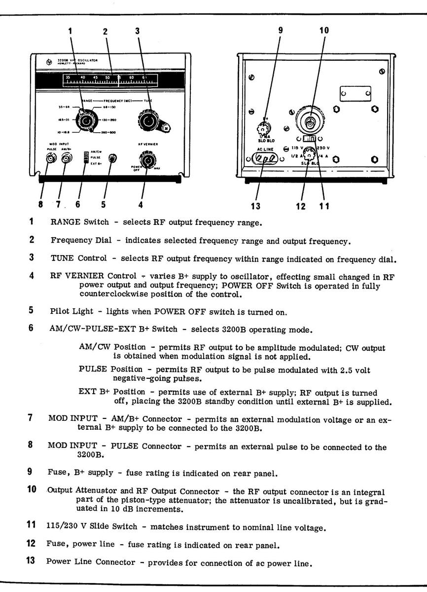
NOTE
With the modulation switch in the AM/CW position, no resistance less than 1 K ohm should be connected across the MOD INPUT - PULSE connector. A low resistance will change the -6 V bias to the pulse modulation circuit sufficiently to reduce or stop the RF oscillator output.
3-15. PULSE MODULATION. Prepare the 3200B for the pulse modulation operating mode as follows:
a. Set modulation switch 6 to PULSE position.
b. Connect modulation signal to MOD INPUT-PULSE connector 8 ; the modulation signal shall consist of negative-going pulses, not exceeding a peak amplitude of 2.5 V.
NOTE
In this operating mode the RF oscillator is shut off between pulses, thus the on-off ratio for pulse modulation is very high.
3-16. EXTERNAL B+ OPERATION. Prepare the 3200B for external B+ operation as follows:
a. Set modulation switch 6 to EXT B+ position.
b. Connect external B+ to MOD INPUT-AM/B+ connector 7; the external B+ supply shall have a maximum voltage of 135 volts and a current capacity up to 40 mA.
NOTE
With the modulation switch in the EXT B+ position, no resistance less than 1 K ohm should be connected across the MOD INPUT-PULSE connector. A low resistance will change the -6 V bias to the pulse modulation circuit sufficiently to reduce or stop the RF oscillator output.
3-17. OPERATIONAL GUIDE
3-18. In the practical application of the 3200B, the following information should assist in providing more accurate results as the capabilities and limitations of the instrument are expanded upon.
3-19. OUTPUT LEVEL
3-20. Operating efficiency in a wide-band oscillator varies across the entire band. Thus, the output power also varies. The typical maximum output over the range of the 3200B is shown in Figure 3-2. The maximum output into 50 ohms has been determined by observing the output of the 3200B, while adjusting the probe, without regard to probe calibration markings.
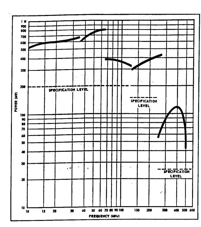
Figure 3-2. Typical Maximum Power Output
3-21. RF DISTORTION
3-22. The basic oscillator used in the 3200B has two tubes operated in push-pull. In the normal balance condition between the tubes, the push-pull operation suppresses the even-harmonic content of the output waveform. The output of the 3200B is
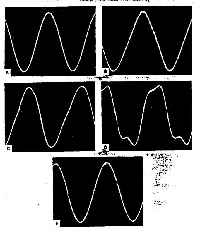
Figure 3-3. Typical RF Output Waveforms
sinusoidal with very low distortion. Using a high frequency sampling oscilloscope (such as the -hp-185B), the RF waveform may be observed directly The oscilloscone natterns in Figure 3-3 show the twoical output of the 3200B at various frequencies Figure 3-3A is the output waveform at 100 MHz Figure 3-3R and 3-3C are RF waveforms at 400 MHz and 500 MHz respectively. At the higher frequencies, and at lower output levels, the waveshape departs slightly from sinusoidal as the slope of the curve through the baseline resembles a straight line. With a very low output level at 460 MHz even harmonics show up in the waveform as in Figure 3-3D This condition is due to the lack of norfeet electrical balance between two tube circuits, which is normal. as lead lengths and tube and component characteristics differ slightly. At the higher output levels, and on the high frequency range, the RF waveshape again resembles the shape shown in Figure 3-3A. By the use of a low-pass filter, the output waveshape may be restored to its original shape, as in Figure 3-3E.
3-23. TYPICAL DRIFT
3-24. The output level of the 3200B is quite stable for long periods of time. However, the frequency will drift slightly. Also, after complete warmup, the frequency stability will change as a result of switching ranges or readjusting the frequency dial. Typical frequency drift (for 5 minutes after a 4hour warmup), on the various ranges, is shown in Figure 3-4. The drift is shown as a percentage of the initial frequency setting.
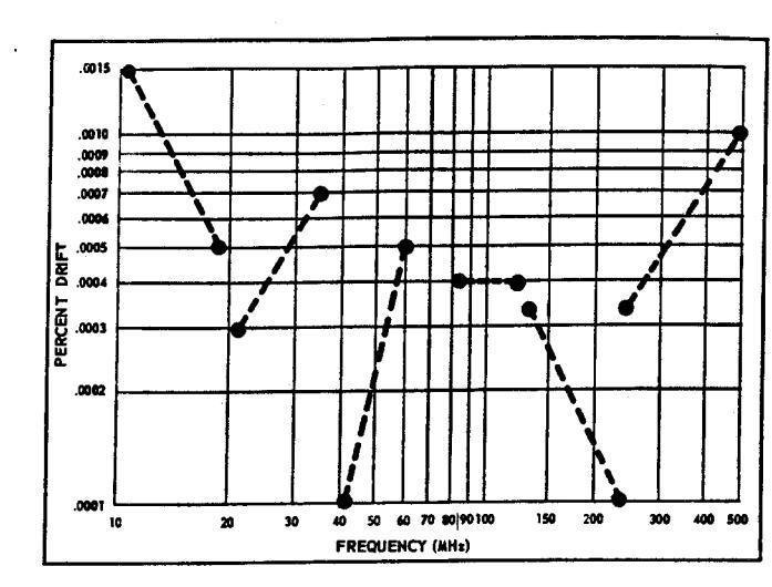
Figure 3-4. Typical Frequency Drift
3-25. FREQUENCY RESPONSE (MODULATION)
3-26. The 3200B is amplitude modulated by capacitively coupling a modulating signal to the Oscillator tube plate voltage supply. The modulated dc is fed via a low-pass filter, into the RF housing. This filter must have a relatively low audio cut-off frequency to prevent RF leakage at the lowest RF frequency of 10 MHz. However, the response is essentially flat across the audio range from 200 Hz to 100 kHz. Figure 3-5 shows the typical frequency response with RF frequencies of 10 MHz and 100 MHz.
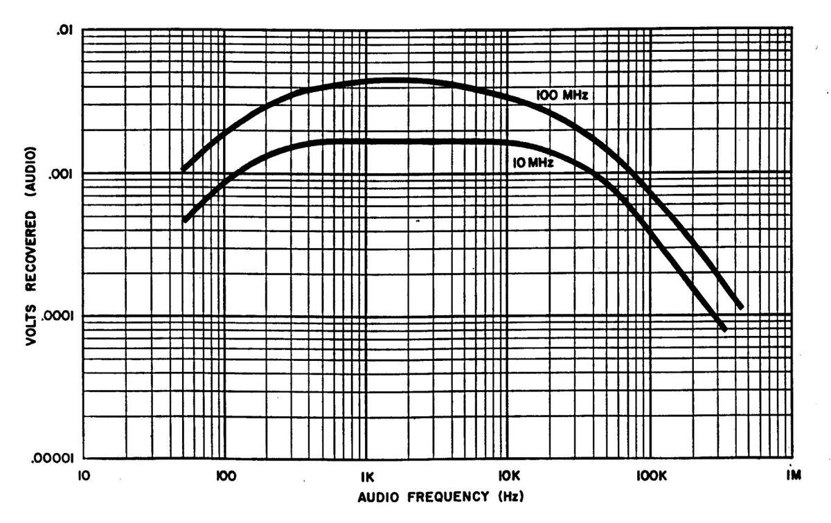
Figure 3-5. Typical Frequency Response
3-27. AMPLITUDE MODULATION
3-28. The 3200B can be used at higher than 30% AM. The 30% AM at less than 1% distortion (See Specifications, Section I) is a limitation because of lack of external control of the internal power supply. The design of the 3200B is such as to allow operation with an external variable dc supply. Depending on the source used, the audio signal may be transformer or capacitively coupled to the dc supply. This composite ac and dc signal is connected to the AM/B+ connector with the modulation input switch in the EXT B+ position. The only limitation
of this method of modulation is that the dc supply voltage plus the rms voltage of the modulation signal must not exceed 135 volts. (This is the tube manufacturer's design maximum.) One hundred percent modulation is possible with this mode of operation. Recovered audio distortion for 90% amplitude modulation with 1 V rms RF output has been found to be typically less than 3% at 10, 20, 40, 80, 150, 250, 400, and 500 MHz.
3-29. It should be noted that the RF output may not meet the specified levels with this system.
Figure 4-1. Block Diagram 3200B
Figure 4-3. Amplitude Modulation 3200B
Figure 4-2. RF Oscillator Circuits
SECTION IV PRINCIPLES OF OPERATION
4-1. GENERAL
4-2. The 3200B VHF Oscillator, shown in the block diagram (Figure 4-1), covers the frequency range from 10 to 500 MHz with six overlapping bands. This instrument was designed primarily as a high output source of CW. Circuitry has been incorporated to allow both amplitude and pulse modulation. A variable, piston-type, waveguide-below cutoff attenuator is used to control the output.
4-3. RF OSCILLATOR
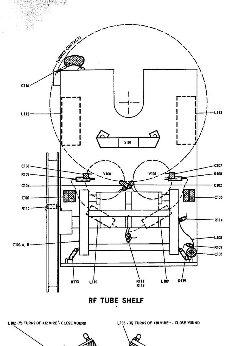
4-4. The oscillator circuit, shown in Figure 4-2, generates all of the radio frequencies in the 10 to 500 MHz range of the instrument. The circuit employs two 6DZ4 triodes with push-pull connected plates and grounded cathodes. Simple, fixed feedback is accomplished by means of capacitive dividers consisting of C102 and C104, together with the grid-to-cathode capacitance of the triodes. Chokes L109 and L110, along with good cathode grounding and short grid connections, serve to maintain high grid circuit impedance, preventing phase shift in the feedback voltage divider and consequential oscillation in the circuit at parasitic frequencies.
4-5. Tuning of the oscillator is accomplished by means of a tank circuit which includes coils L101 to L106 and capacitors C103A and C103B. There are six different tank coils: one for each frequency range. The coils are wrapped on a specially formed turret which is detented into one of six frequency range positions by the RANGE switch on the front panel. Wiping contacts are used to connect the selected coil into the tank circuit. The center of each tank coil is neutral and is used as a feed point for plate power, which is connected through a switch operated by the turret drive and a common supply ring on the turret. One hundred ohm resistors (R101 to R106) are connected between the coils and the B+ feed point to break up undesirable RF paths, without introducing appreciable plate voltage or RF loss.
4-6. ATTENUATOR
4-7. The output from the oscillator is coupled to a pickup loop (L107) mounted at the end of a piston in the waveguide-below-cutoff attenuator. The distance between the pickup coil and the output coils on the turret is a fixed amount with the probe fully inserted. With this dimension fixed on each fre-
quency range, the coupling is different. On the high range, with the attenuator probe at maximum penetration, the pickup coil becomes overcoupled to the output coil. In some instances, this overcoupling loads the tuned output circuit to an extent which causes the oscillator to stop. Overcoupling will also cause frequency "pulling" creating dial errors. With this type of attenuator setup, the maximum penetration does not mean maximum output.
4-8. MODULATION
4-9. Amplitude modulation of the 3200B is accomplished by capacitance coupling a modulating signal to the oscillator plate supply. This is shown in block diagram form (Figure 4-3). With this type of modulation, up to 30% AM is possible with less than 1% distortion at input frequencies from 200 Hz to 100 kHz.
4-10. Pulse modulation of the 3200B is explained by the circuitry of Figure 4-4. With no signal input, a -32 volt bias is applied to the oscillator tube grids through R401, junction A, L109, L110, R107, and R108. This bias will stop tube conduction, thereby stopping oscillation. Thus, with no input signal, there will be no output from the 3200B.
Figure 4-4. Pulse Modulation 3200B
Principles of Operation
4-11. A 2.5 volt negative-going pulse applied to the base of transistor Q401 will cause the transistor to conduct as the pulse approaches the negative peak. The impedance between the emitter and collector will decrease sufficiently to dissipate the -32 volt bias across R401. This puts junction A at a very low impedance with respect to ground, allowing the tubes to oscillate. As the pulse starts in the positive direction returning to zero potential, the transistor stops conduction, restoring the -32 volt bias to the oscillator tube grids which stops the oscillator. Essentially, the transistor becomes a fast action switch controlling the -32 volt bias to the oscillator grids.
4-12. The circuitry to the base of the transistor has resistors to limit the input impedance of the PULSE input connector and diodes to limit voltage, which could cause damage to the transistor.
4-13. Positive-going pulses to the pulse input connector, with Mod Input Switch in "PULSE" position, will result in no output from the instrument.
4-14. EXTERNAL B+ OPERATION
4-15. In the external B+ mode of operation, the internal plate voltage supply is disconnected. The plate supply lead is connected to the AM/B+ connector. A controlled external power supply connected to the AM/B+ connector will produce CW operation of the instrument. During external B+ operation a -6 volt bias is connected internally to the grid switch transistor, Q401, to keep it in the "ON" condition removing the -32 V bias from the oscillator grids. This circuitry is shown in the block diagram (Figure 4-5).
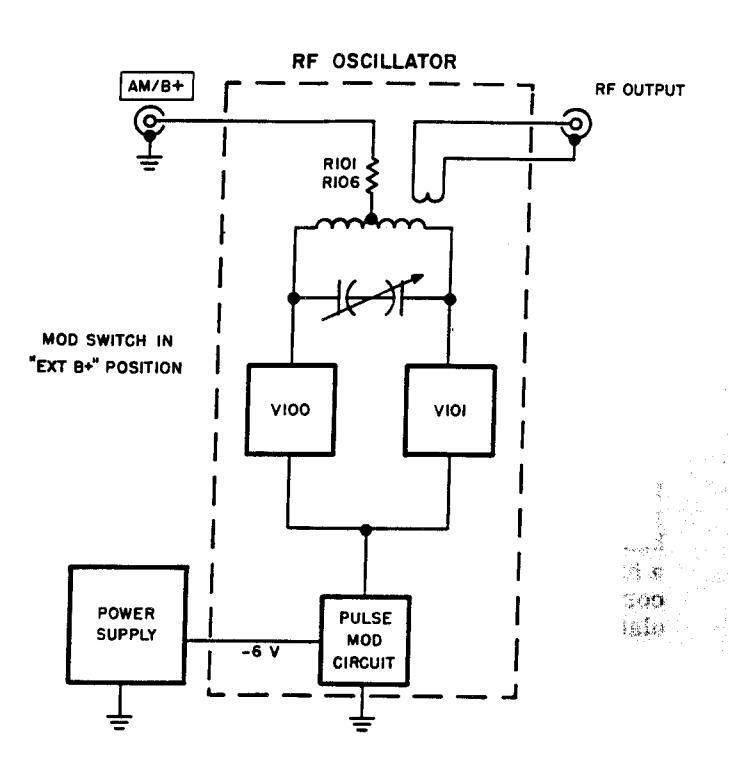
Figure 4-5. External B+ Operation
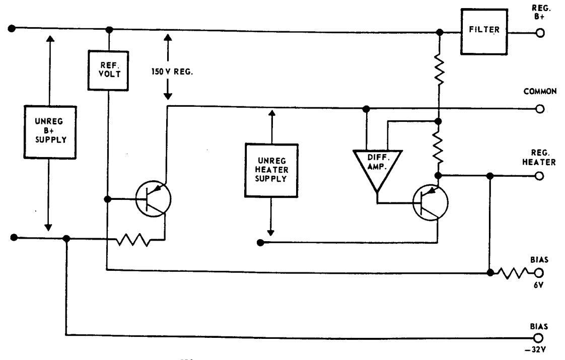
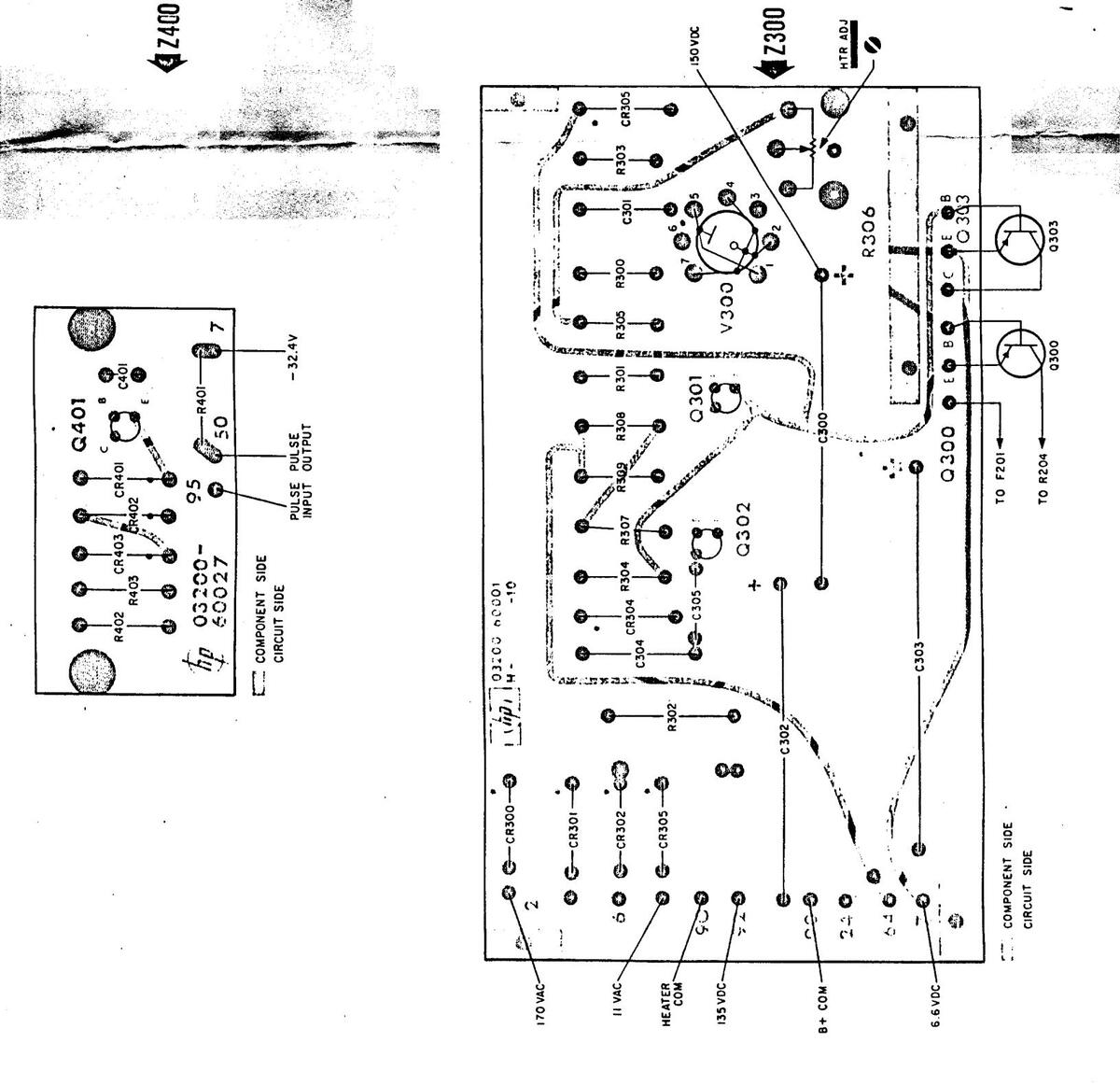
4-16. The Power Supply consists of two regulated supplies having a common power transformer. The outputs are 150 vdc, 40 mA for the oscillator tube plate supply, and 6.6 vdc, 450 mA for the oscillator tube heater supply. The regulated supplies are also a source of bias for operating the pulse modulation circuit (Z400). A -6 V bias is provided to operate the pulse modulation circuit, and -32 V is provided to turn off the oscillator. A block diagram of the complete supply is shown in Figure 4-6.

SECTION V MAINTENANCE
5-1. INTRODUCTION.
5-2. The 3200B VHF Oscillator is a very compact instrument, which generally makes equipment difficult to maintain. However, by use of the disassembly procedure for troubleshooting and repair, as described under Mechanical Disassembly Procedures, this instrument can be readily serviced or maintained.
5-3. LUBRICATION
5-4. The 3200B is adequately lubricated for the life of the instrument. Added lubrication is necessary only when lubricants are wiped off during replacement of parts. The instrument should be checked periodically. If the lubrication on the drum dial shaft or the frequency shaft becomes thick, a small amount of light oil should be added to thin the "Molykote" on the shafts. The detent roller should be inspected for lubrication at the bearing. "Molykote G" (-hp- Stock No. 6040-0024) or equivalent should be used on this bearing.
5-5. TEST EQUIPMENT REQUIRED
5-6. The test instruments required to perform the operations of Section V are listed in Table 5-1. They are listed by type and specification. A recommended instrument is also given, however, other instruments may be used provided their performance equals or exceeds the critical specifications.
5-7. PERFORMANCE CHECKS
5-8. The procedures of paragraphs 5-9 through 5-18 check the 3200B VHF Oscillator for incoming inspection, periodic evaluation, calibration, and troubleshooting. The tests can be performed without instrument cover removal. The specifications of Table 1-1 are the performance standards.
5-9. RF RANGE AND ACCURACY
5-10. Connect the Electronic Counter/Converter (with a 10-dB attenuator) to the RF output of the 3200B, withdraw the attenuator probe to the first mark (approximately 1/2 inch), set the RF VER-NIER to its maximum position, and allow a minimum of 1/2 hour warmup. On each frequency band, check the frequencies listed in Table 5-2, setting the pointer on each nominal frequency shown. The
frequencies, as read on the Electronic Counter, must fall within the limits shown in Table 5-2. This instrument must be capable of producing all of the nominal frequencies shown with no more than 2% off-scale movement of the pointer.
5-11 RF STABILITY
CAUTION
The -hp- 5253B Frequency Converter and the -hp- 431B Power Meter may by damaged by overload. Extreme care must be used when operating these instruments with the 3200B, which has a high power RF output.
5-12. Adjust the frequency of the 3200B to 100 MHz and allow the instrument to warmup for 4 hours (line voltage set to 115 V). Set RF VERNIER in MAX position and proceed as follows:
a. With attenuator probe withdrawn to the last calibration mark, attach the Power Meter to the RF output connector.
b. Slowly insert attenuator probe until the Power Meter reads 0.2 mW (-7 dBm). (This is an arbitrary value and need not be exact.)
c. Disconnect Power Meter and connect the Frequency Counter/Converter to the RF output connector.
d. Readjust the 3200B Frequency Control until the counter reads approximately 100 MHz.
e. Note counter reading and allow instrument to operate for 5 minutes. The reading should be within 0.002% of original frequency reading. At 100 MHz this is ±2 kHz.
f. The reading after 1 hour should be within 0.02% of original frequency reading. At 100 MHz this is ±20 kHz.
g. Readjust the line voltage from 115V to 120V. Note counter reading. The frequency must not change by more than 0.001% of reading in step f. At 100 MHz this is ±1 kHz.
TABLE 5-1. TEST EQUIPMENT RECOMMENDED
| Instrument Type | Critical Specifications | Recommended Instrument |
|---|---|---|
| Electronic Counter | Frequency Range: 0 - 500 MHz | -hp- 5245L with -hp- 5253B Plug-in |
| Power Meter |
Frequency Range: 10-500 MHz
Power Range: +10 dBm to -15 dBm or 10 dBw to -30 dBw (-hp-434A) |
-hp-431B with -hp-478A
Thermistor Mount or -hp-434A |
| 10-dB Attenuator | To extend power range of the -hp- 431B and to pro- | -hp- 8491A |
| 20-dB Attenuator | tect the electronic counter input itom mga power | -hp- 8491A |
| VHF Oscillator |
RF Range: Same as 3200B
Output: Same as 3200B |
-hp- 3200A/B |
| Oscilloscope |
Frequency Range: 450 kHz
Sensitivity: 1 mV/cm |
-hp- 130C |
|
High Output
Audio Oscillator |
Output: 3 W (42.5 V) across 600 ohms | -hp- 201C or -hp- 205AG |
| Diode Mixer | Frequency Range: Same as 3200B | -hp- 10514A |
| Electronic Voltmeter | AC-DC Voltage Range: to 300 V, Accuracy: ±2% | -hp- 410C |
| Distortion Analyzer |
Frequency Range: 200 Hz to 100 kHz
Distortion Range: Less than 1% |
-hp- 331A |
| 50-ohm Termination | Capable of handling 1/2 W | -hp- 908A |
| Power Supply | 0 to 7.5 V | -hp- 6203A |
|
Probe Coax T
Connector |
For use with the -hp- 410C Electronic Voltmeter | -hp- 11042A |
TABLE 5-2. RF ACCURACY LIMITS
|
Nominal
Frequency (MHz) |
Upper
Frequency Limit (MHz) |
Lower
Frequency Limit (MHz) |
|---|---|---|
| 10 | 10.2 | 9.8 |
| 18.5 | 19.176 | 18.424 |
| 18.5 | 18.87 | 18.13 |
| 35 | 35.7 | 34.3 |
| 68 | 69.36 | 66.64 |
| 130 | 132.6 | 127.4 |
| 260 | 265.2 | 254.8 |
| 500 | 510 | 490 |
5-13. RF OUTPUT
5-14. To measure RF power output proceed as follows:
a. Connect a 20-dB attenuator and power meter to the RF output connector with the 3200B attenuator near minimum output.
b. Set the 3200B RANGE switch to the 10-18.8 MHz range.
c. Insert 3200B attenuator probe until power meter reads 2 mW. Check RF output across the band, readjusting 3200B attenuator probe if power meter reading drops below 2 mW. Because coupling is not directly related to insertion distance maximum power may result with less than maxmum insertion. In addition, overcoupling the probe may load the oscillator enough to shift its frequency.
d. Repeat step c on 18.5-35 MHz, 35-68 MHz, and 68-130 MHz ranges.
e. Set the 3200B RANGE switch to the 130 - 260 MHz range.
f. Insert 3200B attenuator probe until power meter reads 1.5 mW. Check RF output across the band, readjusting the 3200B attenuator probe if power meter reading drops below 1.5 mW.
g. Set the 3200B attenuator for minimum output with RANGE switch in 260 - 500 MHz range.
h. Remove the 20-dB attenuator and replace it with the 10-dB attenuator.
i. Insert 3200B attenuator probe until power meter reads 2.5 mW.
CAUTION
When setting the attenuator, the probe must not be completely inserted in the tube while the instrument is operated at the low frequency end of the 260 to 500 MHz range. The loading on the oscillator by the attenuator could cause the oscillator to stop. In this condition, the tubes will draw excessive current causing the B+ supply fuse to open.
j. Check the output across the band, readjusting the 3200B attenuator probe if the output drops below 2.5 mW.
5-15. AM RANGE AND DISTORTION
5-16. Connect the equipment as shown in Figure 5-1, set the 3200B under test to any convenient frequency, and proceed as follows:
a. With input to MOD INPUT -AM/B+ on 3200B temporarily disconnected, adjust the second VHF Oscillator for zero beat as observed on oscilloscope. (Use oscilloscope internal sweep for this setup.)
b. Adjust the second VHF Oscillator away from zero beat until a clean rectangle is observed (Figure 5-2A).
c. Connect the audio oscillator to the MOD IN-PUT-AM/B+ terminal on the 3200B under test. Set the audio frequency between 200 Hz and 20 kHz.
d. Adjust the audio oscillator output to form a trapezoid which has a long vertical side of 10 oscilloscope divisions and a short vertical side of 5.39 oscilloscope divisions (Figure 5-2B). (The oscilloscope pattern width is not important but must be kept within screen limits for observing sides of pattern.) At this point, the RF output is amplitude modulated 30%.
e. Connect the AC VTVM across the MOD IN-PUT-AM/B+ connector. The meter reading shall be 20 V ±7 V.
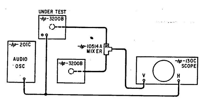
Figure 5-1. AM Characteristics Setup
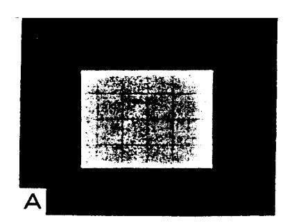
Figure 5-2. AM Characteristics Oscilloscope Displays
f. Disconnect the 3200B used as a beat frequency oscillator and add the 50-ohm termination in its place at diode mixer. Replace the oscilloscope with the distortion analyzer.
g. Measure the distortion of the recovered audio.
h. Without changing the audio oscillator setting, measure the audio oscillator distortion directly. The difference in distortion between the recovered audio frequency and the output of the audio oscillator should be less than 1%.
5-17. EXTERNAL PM REQUIREMENTS
5-18. Connect the equipment as shown in Figure 5-3, and proceed as follows:
a. Disconnect the power supply temporarily and set the 3200B for AM/CW operation with an output frequency of 100 MHz. (This frequency is not critical and may be changed to suit equipment available for this test.)
Figure 5-3. PM Requirements Setup
1.11
c. Connect the power supply to the MOD IN-PUT-PULSE connector. Change the modulation input switch to the PULSE position.
d. Increase the power supply output until the level indicated on the oscilloscope is the same as in step b.
e. Measure the dc voltage level of the power supply. The dc voltage should be -2.5 volts or less.
5-19. TROUBLESHOOTING AND REPAIR
WARNING
Removing the top cover of the instrument exposes the power transformer secondary winding connections on the printed circuit board which constitutes a shock hazard if the instrument is operated in this condition.
5-20. TROUBLESHOOTING CHART
5-21. The Troubleshooting Chart, Figure 5-4, is in the form of a troubleshooting tree. The tree shows a logical sequence to be used for determining a
.......................................
fault when the power output from the 3200B is too low or when there is no output. Follow each step toward the normal (T-true) or abnormal (F-false) condition as determined by indicated tests.
5-22. TUBE AND SEMICONDUCTOR REPLACEMENT
5-23. All tubes and semiconductors are easily accessible after the 3200B is disassembled for troubleshooting and repair as described under Paragraph 5-32.
5-24. TRANSISTOR INSULATORS
5-25. Some of the transistors in this instrument are insulated electrically from the heat sink. For maximum transfer of heat to the heat sink through the insulator, it is coated on both sides before assembly with silicone grease (-hp- Stock No. 8500-0059). If these transistors are replaced, the replacement should also be coated with the grease.
5-26. VOLTAGES
5-27. Voltages shown in the schematic, Figure 5-12, indicate the normal operating conditions for the 3200B while in the troubleshooting condition. (RF shield removed and no load on the output.) Voltages were measured with a -hp- 410B VTVM. They indicate typical operation and do not constitute specifications.
Figure 5-4. Troubleshooting Tree - Power Output
5-4
N 15 Par.
The second
Figure 5-5. Troubleshooting and Repair Setup
5-28. MECHANICAL DISASSEMBLY PROCEDURES
5-29. COVER REMOVAL
5-30. TOP AND BOTTOM COVERS. Remove two screws at the rear of the instrument. Slide cover toward the rear of the instrument to disengage lip at front panel.
5-31. SIDE COVERS. Remove four screws from each side cover. Top and bottom covers need not be removed to remove side covers.
5-32. TROUBLESHOOTING AND REPAIR SETUP
5-33. Refer to Figure 5-5 and proceed as follows:
a. Remove top, bottom, and side covers.
b. At rear of instrument, remove attenuator probe. Rotate attenuator retaining ring one complete turn. Slide retaining ring and locking spring off of attenuator tube. Locking pin will remain in tube. During reassembly of retaining ring, the pin must be pressed back in place.
c. Remove plug P200 from receptacle J200.
d. At right side of the instrument, remove the two screws retaining the rear panel and one screw retaining the printed circuit board.
e. At left side of the instrument, remove the one screw retaining the front panel switch plate and the two screws retaining the RF base plate assembly.
f. Carefully separate the instrument into two pieces. The left side and rear panel constitute one piece. The right side and lower front panel constitute the second piece.
NOTE
Care should be taken as the upper front panel, front panel window, and window mask will be loose parts and should be removed during troubleshooting and repair procedures.
g. Remove four screws retaining the RF shield casting and slide it carefully away from the RF base plate assembly.
h. Replace P200 plug in J200 receptacle.
5-34. The 3200B is now in operating condition. The attenuator probe may be placed in approximately normal position by reversing the RF shield casting.
5-35. FRONT PANEL DISASSEMBLY
5-36. Remove top, bottom, and side covers, and proceed as follows:
a. At left side of the instrument, remove the one screw retaining the front panel switch plate, two screws retaining the RF base plate assembly. At right side, remove one screw retaining the printed circuit board.
b. At left side of the instrument, loosen the two screws retaining the rear panel.
c. At right side of the instrument, remove one screw retaining the front panel switch plate.
d. Using a 5/64 inch Allen wrench, remove the two front panel control knobs.
e. Carefully separate the left side frame from the front panel.
NOTE
Care should be taken as the upper front panel, front panel window, and window mask will be loose parts and should be removed during this procedure.
f. Carefully separate the right side frame from the front panel. The front panel will be restrained only by the wires attached.
5-37. TURRET ASSEMBLY REMOVAL
5-38. The turret assembly may be readily removed with the 3200B in the troubleshooting and repair condition. However, the turret position on the shaft is very critical and the RF frequency alignment should be checked after replacement. (See RF Calibration, Paragraph 5-44 before removing turret).
5-39. DIAL STRINGING PROCEDURE
5-40. The dial stringing should be done with the front panel disassembled, but not disconnected from the instrument. Refer to Figure 5-6 and proceed as follows:
a. Using approximately 4 feet of 0.027 inch diameter, nylon covered, glass core dial cord, thread about 15 inches of cord through the right side hole in the cursor.
b. Loop the cord once around pin on cursor and thread balance of cord through left side hole in the cursor.
c. Thread the 15-inch section of cord around the small right side pulley, through the RF base plate, and around the large pulley to the "start" pin on the large pulley.
d. At this point, the notch in the large pulley should face the rear of the instrument (±45°), and the dial pointer should be near the 10 MHz calibration mark. Secure the dial cord on the pin.
e. Thread the dial cord around the small left side pulley, the angle pulley, etc. as shown in Figure 5-6.
f. Before securing the cord on the dial spring, adjust tension so as to extend spring no more than 1/8 inch.
g. The frequency control should be rotated to the extremes of the dial travel to assure proper operation.
Figure 5-6. Dial Stringing
h. With the tuning capacitor fully meshed, the dial pointer should be 1/32 to 1/16 inch to the left of the 10 MHz calibration mark. Required adjustment can be made by slipping the pulley on the tuning capacitor shaft.
5-41. ADJUSTMENT AND CALIBRATION
5-42. Any tolerances listed in this section are the limits indicated by the Specifications in Table 1-1. Factory adjustments are made to considerably closer tolerances. Field adjustments to closer than specified tolerances are possible if time and patience are used.
5-43. POWER SUPPLY,
a. Connect the 3200B to a power source set to 115 V. Connect the VTVM (dc function) from junction CR305-R303 (-) on printed circuit board and chassis ground (+).
b. Heater voltage should be -6.6 ±0.13 vdc. Readjust R306 (Htr Adj) if required. (-6.6 V at power supply is equivalent to -6.0 V at tube socket terminals.)
c. Change input voltage to 125 V and then 105 V. Heater voltage must be within ±2% of voltage in step b.
d. Disconnect the VTVM and connect the oscilloscope in its place.
e. The ac signal on the heater line must be less than 50 mV P-P.
f. Change the oscilloscope connections to points across capacitor C302.
g. The ac signal on the B+ supply line must be less than 20 mV P-P.
h. Disconnect the oscilloscope and connect the VTVM between chassis ground and pin #1 or #5 of V300.
i. The B+ supply voltage should be 150 V ±10 V.
5-44. RF CALIBRATION INCLUDING TURRET RE-ASSEMBLY PROCEDURES. After the original factory calibration, the only reason for recalibration would be as a result of replacing the turret, a critical component mounted on the tube shelf, or the complete tube shelf assembly. Before attempting turret disassembly or frequency calibration, the following information should be noted:
a. The original turret may be removed and replaced without complete calibration, if it is replaced as precisely as possible in its original position on the shaft. A scribe mark on the shaft can be used as a guide for position along the shaft. The turret contacts should be centered on the capacitor contacts.
b. The position of the turret along the shaft is restricted by the ability of the turret to operate Switch S101 on the two lower frequency ranges; also, the ability of the turret tuned circuit on the 260 to 500 MHz range to allow the instrument to tune the range required.
c. The normal mechanical tolerances of the holes used for mounting the RF shield casting is such as to affect the calibration. Shifting the castting slightly will change frequency and output power slightly so the correct position should be checked electrically.
d. The attenuator probe must be properly oriented with respect to the turret. Changing the turret could result in mechanical interference.
e. There is circuitry in the 3200B used to suppress parasitics. C108 is the only adjustable component which serves this purpose. For adjustment of C108, see Paragraph 5-46. The other circuitry is not adjustable but is controlled by component position and lead length. If replacement is required, these parts should be replaced as close as possible to their original position. The suppressor circuits consist of:
- (1) C117 and R110
- (2) C119, R111, and R112
- (3) C120, C108, R109, and L108
- (4) C121, R113, and R119
f. The calibration of this instrument can norformed with the RF shield removed and the attenuator probe supported in a position approvimately 1/2 inch from the turret simulating its normatery 1/2 men from the turret simulating its norcrease the frequency by nominally 1%. For increased accuracy, the instrument should be checked with the shield in place. To touch-up the core adjustment of any or all of the four lower frecurrent contraction and of an of the four lower meto gain access to the core. The access hole is loto gain access to the core. The access hole is toswitch to place the required turnet coil in position for adjustment. A trial and error procedure will have to be followed. To decrease inductance, rotate core in clockwise direction.
g. If the overall calibration of the 3200B is off by approximately the same amount and in the same direction (either too high or too low) the pulley on the tuning capacitor may be slipped on the shaft to compensate for the error.
h. Changing tubes or normal aging of components in the 3200B should not require complete recalibration of the instrument. Typically the change in frequency is within the normal tolerance specified for the 3200B.
5-45. TURRET REASSEMBLY.
a. Set RANGE switch to the 10-18.8 MHz range.
b. Slide the turret on the shaft so that the turret contacts do not touch the capacitor contacts when the turret is moved along the shaft.
c. Rotate the turret until the turret contacts are centered on the capacitor contacts, and tighten set screws enough to hold turret in place.
d. On the lower two ranges, Switch S101 must be operated by the cam on the turret.
e. Change RANGE switch to the 260-500 MHz range and check end frequencies (260 and 500 MHz) using a frequency counter.
- (1) If an original turret is being reassembled, the range should be correct but the dial settings may be off (either too high or too low). In this case, the turret may be moved closer to the front of the instrument to increase the output frequencies, or toward the rear to decrease the frequencies. Only a few thousandths of an inch movement will be required.
- (2) If a new turret is being assembled on the shaft, the new turret should be set as closely as possible to the original turret position and the calibration procedure used for adjustment.
-
f. Check the other five ranges to assure proper calibration. (See Calibration Procedure, Paragraph 5-46 for adjustment, if required.)
5-46. CALIBRATION.
NOTE
See Troubleshooting and Repair Setup, Paragraph 5-32.
a. The RF shield cover should be reversed so it may be used to hold the attenuator probe in a somewhat normal position about 1/2 inch from the turret.
b. Connect the equipment as shown in Figure
Figure 5-7. RF Calibration Setup
c. Set the RANGE switch to the 260-500 MHz range. Check the frequency at 260 and 500 MHz. The counter should read within ±2% of dial setting. If not, adjust the inductance of the inductor for this range by adding or removing solder from the slots in the inductor. For a small change in the inductance, the turret may be moved along the shaft.
- (1) Move the turret away from the RF tube shelf to increase the inductance in the capacitor contacts. This effectively reduces stray capacitance between the turret and the tube shelf.
- (2) Move the turret toward the RF tube shelf to decrease the inductance in the capaci-
tor contacts. This increases the stray capacitance between the turret and the tube shelf.
d. At 260 MHz, adjust the attenuator probe for maximum output. This should be 25 mW (approximately 1.1 V on the VTVM, assuming ideal conditions). Adjust C108 for maximum output as read on the VTVM.
e. Set RANGE, switch to the 130-260 MHz range. Check 130 and 260 MHz frequencies. The counter should read within ±2% of dial settings. If not, adjust inductance by bending coils to increase or decrease inductance.
f. The four lower frequency ranges should be checked and inductances adjusted by means of the ferrite core in each inductor.
NOTE
If any of these coils required adjustment, the coils should be recoated with Communications Products Co. "Q-max A-27".
g. Replace the RF shield cover and the attenuator. The four mounting screws should be adjusted so as to exert equal pressure at each screw.
h. Check power output on all ranges. The power output must be greater than:
- (1) 200 mW (3.2 V across external 50 ohms) on the 10 - 18.8 MHz, 18.5 - 35 MHz, and 68 - 130 MHz ranges.
- (2) 150 mW (2.7 V across external 50 ohms) on the 130 - 260 MHz range.
- (3) 25 mW (1.1 V across external 50 ohms) on the 260 - 500 MHz range.
5-47. For more accurate measurement of the output power, the -hp- 431B Power Meter (or equivalent) with an -hp- 478A Thermistor Mount is recommended in addition to a low VSWR 20-dB attenuator.
SECTION VI REPLACEABLE PARTS
6-1. INTRODUCTION
6-2. This section contains information for ordering replacement parts. Table 6-1 lists parts in alpha-numerical order of their reference designations and indicates the description and -hp- Stock Number of each part. An Illustrated Parts Identification follows Table 6-2 giving mechanical breakdown of the 3200B. Adjacent tables, keyed to Figures 6-1 to 6-5, indicates the -hp- Stock Number and description.
6-3. ORDERING INFORMATION
6-4. To obtain replacement parts, address order or inquiry to your local Hewlett-Packard Sales and Service Office (see lists at rear of this manual). Identify parts by Hewlett-Packard Stock Number.
6-5. To obtain a part not listed, include:
- a. Instrument model and serial number
- b. Description of part
- c. Function and location of parts
| - | REFERENCE DE | SIGNATOR | 8 | ||||||||
| • | • | assembly | Ē | = | mise electronic part | P | plug | v | vecuum tube, neon | ||
| в | * | motor | F | = | fuse | ò | * | transistor | · | bulb, photocell, etc. | |
| BT | = | battery | FL | = | filter | Ř | = | resistor | w | = | cable |
| с | = | capacitor | J | 30 | jack | RT | = | thermistor | x | = | socket |
| CP | - | connecting part | ĸ | = | relay | 8 | 35 | switch | Ÿ | ¥ | crystal |
| CR | = | diode | L | = | inductor | т | ÷ | transformer | ž | Ŧ | network |
| DL | delay line | м | = | meter | TB | = | terminal board | - | |||
| DS | = | device signaling (lamp) | MP | = | mechanical part | TP | _ = | test point | |||
| - | ABBREVIA | TIONS | |||||||||
| - | CRD | = | ground (ed) | NTD | not field replaceable | DU | - | noundband | |||
| BECU | hervilium comer | H | = | henries | NT PL. | = | nickel plate | PNO | - | rack mount only | |
| BH | binder head | HEX | = | hexegonal | NO | - | normally com | RMS | _ | Tool meen source | |
| BP | = | bandnass | HR | - | hour (s) | NPO | negative positive zero | S-B | - | slow-blow | |
| BRS | brass | TF | ** | intermediate freq | (zero temperature | SCB | - | BOT BION | |||
| CCW | = | counterclockwise | IMPG | = | impregnated | coefficient) | SE | - | selenium | ||
| CER | ceramic | INCD | = | incandescent | NRFR | = | not recommended for | SECT | = | section (s) | |
| CMO | cabinet mount only | INCL | include (s) | field replacement | Si | ч | silicon | ||||
| COEF | = | coefficient | INS | = | insulation (ed) | OBD | = | order by description | SIT. | × | silver |
| COM | * | common | INT | = | internal | OV HD | = | oval head | SI. | = | alide |
| COMP | = | composition | К | = | kilo = 1000 | OX | = | oxide | SPL | ± | anecial |
| CONN | = | connector | LIN | = | linear taper | Р | - | peak | SST | Ξ | stainless steel |
| CP | * | cadmium plate | LKWASH | = | lockwasher | PAN HD | ÷ | pan head | SR | ÷ | split ring |
| CW | = | clockwise | LOG | × | logarithmic taper | PC | = | printed circuit | STL | = | steel |
| DEPC | deposited carbon | LPF | = | low pass filter | PF | - | picofarads = 10 -12 farads | TA | = | tantalum | |
| DR | drive | м | × | milli = 10 -3 | PH BRZ | = | phosphor bronze | TD | = | time delay | |
| ELECT | × | electrolytic | MEG | = | meg = 10 6 | PHL | = | Phillips | TGL | = | toggle |
| ENCAP | = | encapsulated | MET FLM | . = | metal film | PIV | а | peak inverse voltage | TI | × | titanium |
| EXT | external | MET OX | = | metallic oxide | P/0 | = | part of | TOL | = | tolerance | |
| FBR | - | fiber | MFR | - | manufacturer | POLY | = | polystyrene | TRIM | = | trimmer |
| FDTHRU | × | feedthru | MINAT | * | miniature | PORC | = | procelain | μ | × | micro = 10 -6 |
| FET | ж | field effect transistor | MOM | Ξ | momentary | POS | = | position (s) | VAR | ж | variable |
| FH | = | flat head | MTG | Ŧ | mounting | POT | = | potentiometer | VDCW | = | de working volts |
| FIL HD | = | fillister head | MY | = | "mylar" | PP | × | peak-to-peak | w/ | Ξ | with |
| FXD | - | fixed | NC | × | normally closed | PT | = | point | w | = | watts |
| Ge | germanium | NE | = | neon | PWV | = | peak working voltage | ww | × | wirewound | |
| GL | ۰ | glass | nF | * | nanofarad (= 1000 pF) | PZ | = | "pozidrive" | W/O | = | without |
|
Reference
Designation |
Stock
Number |
Description | |||
|---|---|---|---|---|---|
| AT100 | 03200-60011 | Attenuator probe. Includes L107 and J100 | |||
| C101 | 03200-00005 | Trimmer minimum "C" | |||
| C102 | 0160-0434 | C: fxd cer 10 pF 0.1 pF 500 vdcw | |||
| C103 | 5080-1719 | C: var 31.5 pF 700 V calibrated | |||
| C104 | 0160-0434 | C: fxd cer 10 pF 0.1 pF 500 vdcw | |||
| C105 | 03200-00005 | Trimmer minimum "C" | |||
| 0100 | 0100 0010 | C. fud con 10 pF 10% 150 ydow | |||
| C106 | 0160-0919 | C: 1xu cer 10 pr 10% 150 vucw | |||
| C107 | 0160-0919 | ||||
| C108 | 0132-0002 | C: var poly 0.7 - 3pr | |||
| C109, 110 | 0160-0480 | C: IXd cer 1000 pF -20 + 80% 500 vdcw | |||
| C111 | 0160-0415 | C: 1xd cer 100 pF 10% 500 vacw | |||
| C112, 113 | 0160-0345 | C: fxd cer 1000 pF -20 + 80% 500 vdcw | |||
| C114 | 0160-2162 | C: fxd cer 100 pF 20% 500 vdcw | |||
| C116 | 0160-0952 | C: fxd mica 220 pF 1% | |||
| C117 | Not replaceable. P/O 03200-60024 | ||||
| C119-121 | For Ref. only. See schematic notes Table 7-1 | ||||
| C199 | 0160-2163 | C. fyd paper 0 47 uF 20% 100 ydew | |||
| C201 | 0160 0402 | C. frd my 1 0 uF 20% 200 ydow | |||
| C201 | 0100-0452 | C: fxd alum 45 µF 250 vdgw | |||
| C300 | 0170-0040 | C: frd mr 0, 047 //F 10% 200 vdow | |||
| C: find alum 40 (F 10 + 50% 150 videw | |||||
| C302 | 0180-1796 | C: 1xd alum 40 µr -10 + 50% 150 vdew | |||
| C303 | 0180-0345 | C: fxd alum 2000 µF 25 vdcw | |||
| C304 | 0170-0024 | C: fxd my 0, 022 µF 20% 200 vdcw | |||
| C305 | 0140-0054 | C: fxd mica 100 pF 10% 500 vdcw | |||
| C401 | 0160-2006 | C: fxd mica 100 pF 10% 500 vdcw | |||
| CD 200 - 201 | 1001-0020 | Diada Si 600 niv 0.75 A | |||
| CR300, 301 | Diode Si 50 piv 0.75 A | ||||
| CR302-305 | Diode Si 50 piv 0.75 A | ||||
| CR306 | Diode Si 50 pix 0, 75 A | ||||
| CR401-3 | 1301-0049 | Didde 51 50 prv 0. 75 M | |||
| DS200 | 1450-0048 | Light, indicator, power on | |||
| F200 | 2110-0008 | Fuse 125 V 0.5 A SLO-BLO (115 V operation) | |||
| F200 | 2110-0018 | Fuse 125 V 0, 25 A SLO-BLO (230 V operation) | |||
| F201 | 2110-0040 | Fuse 125 V 0.062 A SLO-BLO | |||
| 74.0.0 | |||||
| J100 | 1051 0049 | Not replaceable. P/O A1100 | |||
| J200 | 1251-0043 | Connector female 8 contacts | |||
| J201-202 | 1250-0001 | Connector RF OSM type 2 hole flange | |||
| L101-106 | For Ref. only. P/O Z100 | ||||
| L107 | For Ref. only. P/O AT100 | ||||
| L108 | For Ref. only. Lead inductance NSR | ||||
| L109-110 | 03200-80002 | Choke 80µH | |||
| L112 | 03200-80002 | Choke 80µH | |||
| L113 | 03200-80001 | Choke 17µH | |||
| L114-115 | 00225-80001 | Coil Assy 410 µH | |||
| L116 | 03200-80022 | Coil Assy RF 140µH | |||
| P200 | 1251-0133 | Connector male 8 contacts | |||
| P204 | 1251-0148 | Connector AC power 3 pm | |||
TABLE 6-1. REFERENCE DESIGNATOR INDEX
|
Reference
Designation |
Stock
Number |
Description |
|---|---|---|
| Q300 | 1850-0098 | Transistor PNP Ge 2N458 |
|
Q200
Q301 302 |
1853-0016 | Transistor PNP Si 2N3638 |
| 0303, 302 | 1850-0098 | Transistor DND Ge 2N458 |
| Q303 | 1952 0026 | Transistor DND Si 2N3006 |
| Q401 | 1853-0036 | Transistor PNP 51 2N3900 |
| R101-106 | 0686-1015 | R: fxd comp 100 Ω 5% 1/2 w |
| R107, 108 | 0686-2235 | R: fxd comp 22 KΩ 5% 1/2 w |
| R109 | 0683-3315 | R: fxd comp 330 Ω 5% 1/2 w |
| R110-112 | 0683-1015 | R: fxd comp 100 Ω 5% 1/2 w |
| R113 | 0686-2205 | R: fxd comp 22 Ω 5% 1/2 w |
| R114 | 0683-1015 | R: fxd comp 100 Ω 5% 1/2 w |
| R118 | 0758-0002 | R: fxd met flm 560 Ω 5% 1/2 w |
| R119 | 0686-2205 | R: fxd comp 22 Ω 5% 1/2 w |
| B201 | 0686-6835 | R: fxd comp 68 KΩ 5% 1/2 w |
| R202 | 0698-3635 | R: fxd met ox 680 Ω 5% 2 w |
| D 009 | 9100 1461 | P. comp lin 1 KO 10% 2 25 m. Includes $200 |
| R203 | R: Comp III 1 M2 10% 2.25 w Includes 5200 | |
| R204 |
R: IXU Met 0X 330 % 5% 2 W
D. fud comp 5 1 K0 5% 1/2 w |
|
| R205 |
R: IXU COMP 5.1 KX 5% 1/2 w
D. fvd comp 100 0 5% 1 /2 w |
|
| R300 | 0080-1015 | R: 1x0 comp 100 % 5% 1/2 w |
| R301 | 0686-7535 | R: 1xd comp 75 KM 5% 1/2 w |
| R302 | 0698-0030 | R: fxd met ox 510 Ω 10% 2 w |
| R303 | 0686-6815 | R: fxd comp 680 Ω 5% 1/2 w |
| R304 | 0686-4725 | R: fxd comp 4.7 KΩ 5% 1/2 w |
| R305 | 0686-1825 | R: fxd comp 1.8 KΩ 5% 1/2 w |
| R306 | 2100-0801 | R: var lin 2 KΩ 10% 0.15 w |
| R307 | 0686-3315 | R: fxd comp 330 Ω 5% 1/2 w |
| R308 | 0686-6825 | R: fxd comp 6.8 KΩ 5% 1/2 w |
| R309 | 0686-1215 | R: fxd comp 120 Ω 5% 1/2 w |
| R310 | 0761-0070 | R: fxd met ox 8.2 KΩ 5% 1 w |
| R401 | 0758-0098 | R: fxd met ox 220 KΩ 5% 1/2 w |
| R402, 403 | 0758-0003 | R: fxd met flm 1 KΩ 5% 1/2 w |
| S101 | 02200-00010 | Contact grid switch |
| 5201 | 2100-1461 | Switch POWER OFF Includes R203 |
| 5200 | 2100-1401 | Switch, I ownit of I, mondes 1200 |
| 5201 | 2101-0033 | Switch, slide DD 3 nog |
| 5202 | 5101-0152 | Switch, Shite Dr. 5 pos |
| T200 | 9100-0314 | Transformer, power |
| V100.101 | 1921-0034 | Tube, elect EIA 6DZ4 |
| V300 | 1940-0004 | Tube, elect OA2 |
| W200 | 8120-0078 | Cable Assy |
| XF200, 201 | 1400-0084 | Fuseholder 3 AG fuse extractor post type |
| VO 900 | 1200 0044 | Socket transistor |
|
10000
10000 |
1200-0044 | Socket transistor |
| AQ3U3 | 1200-0044 | |
| XV100.101 | 03200-80010 | Socket, tube, modified NRFR |
| XV300 | 1200-0053 | Socket, tube, 7 pin min |
| 7100 | 03200_60004 | Turret Assy Includes I.101 - I.106 |
| 2300 | 03200-60001 | PC Board Pulse Mod |
| 7400 | 03200-60027 | PC Board, Grid Switch |
TABLE 6-1. REFERENCE DESIGNATION INDEX (CONT)
ু কাল
"我们不是不是我们,我们有什么?"

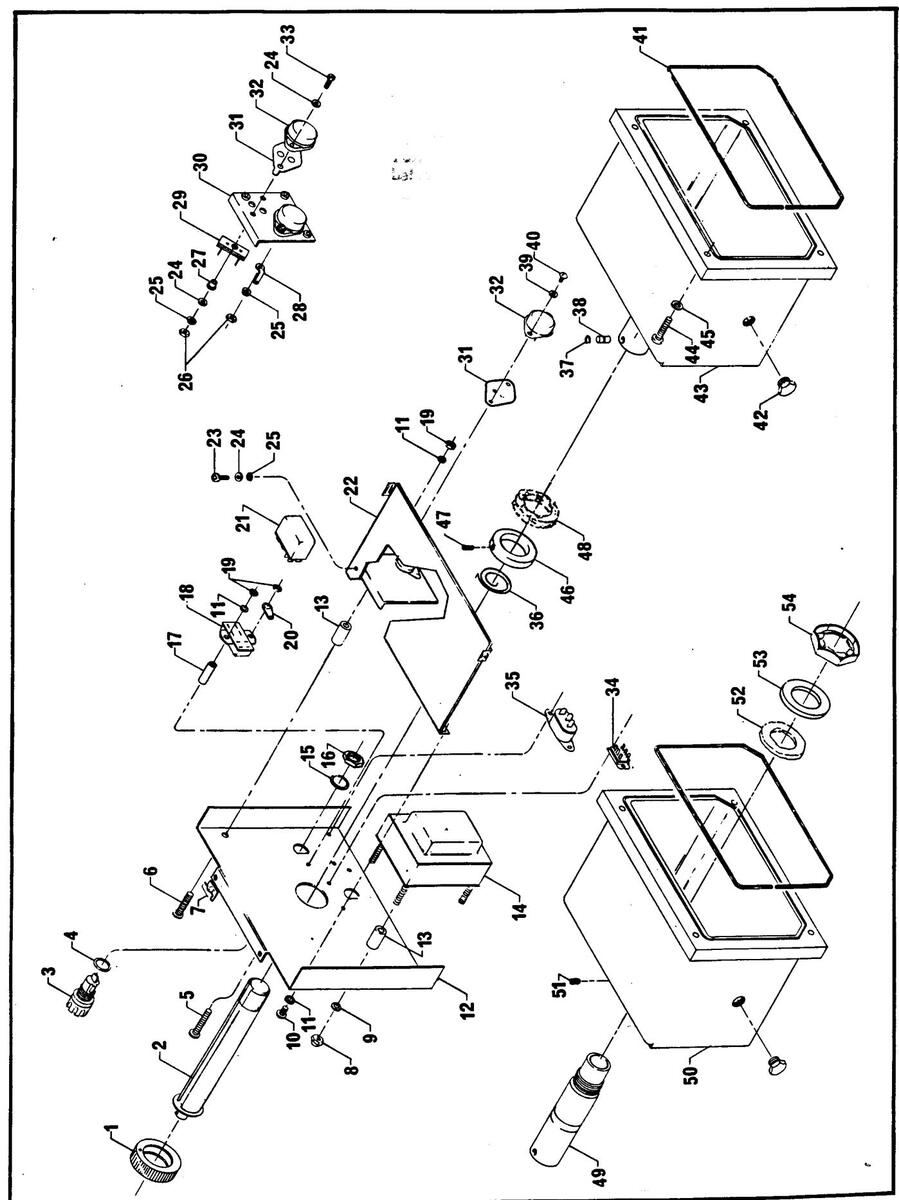
Figure 6-1. -hp- 3200B VHF Oscillator, General Arrangement
| Ref | Illustrations |
|---|---|
| 1 | See Page 6-5, Cabinet Parts |
| 2 | See Pages 6-6 and 6-7, Front Section and Panel Assembly |
| 3 | See Pages 6-8 and 6-9, RF Oscillator Compartment |
| 4 | See Pages 6-10 and 6-11, Rear Section and RF Compartment Cover |
6-4
Figure 6-2. -hp- 3200B VHF Oscillator, Cabinet Parts
| Ref | Part No. | Description | Qty |
|---|---|---|---|
| 1 | 5000-0703 | Side cover | 2 |
| 2 | 5060-0720 | Top cover | 1 |
| 3 | 03200-00021 | Upper front panel | 1 |
| 4 | 03200-20014 | Front panel window | 1 |
| 5 | 03200-80016 | Window mask | 1 |
|
6
7 8 9 10 |
03200-00027
5040-0700 5060-0703 5060-0728 1490-0032 |
Lower front panel
Hinge Side frame assy Foot assy Tilt stand |
|
|
11
12 13 14 15 |
5000-0717
2190-0047 2370-0016 03200-00022 2370-0020 |
Bottom cover
Conical Lockwasher, EXT, #6 Machine screw, 6-32 x 5/16 FH Rear panel Machine screw, 6-32 x 3/16 FH |
1
12 16 1 8 |
| uc |
|---|
| 8881-312 |
| 8 9 4 9 8 |
Front Section and Panel Assembly
6-6
Ref.
Stock No.
03200-20007 03200-60014
2295-0006 2190-0004
4 0
0510-0294
---------------------------------------
3200-20025
3200-20030 3200-20013 3200-60015
3030-0117
0 2 8 4 0 10 8 4 0
3200-60019 03200-20040
0590-0111 03200-20008
1121121121
3050-0316 3050-0274 0510-0235
03200-20041
0360-0270 2700-0015 3030-0033 500-0044
117 113 20
3200-2001
0510-0296 5040-1601
23
3200-20026 3200-60013
03200-60018
25
0360-0393 2470-001 2190-0008
3200-80014 03200-00011
308230
00230-20065
5000-3001 606A-91B
35 43 33
2190-0010 2550-0006
| Qty | 4 4 | ~ ~ | 4 | 4 | - | 0 | - 14 | - က | م | ဂ | 1 | 2 | 21 | 01 0 | 2 - | - 01 | 21 | N - | 010 | N | 20 20 | 4 | 4 | ||||||
|---|---|---|---|---|---|---|---|---|---|---|---|---|---|---|---|---|---|---|---|---|---|---|---|---|---|---|---|---|---|
| Description | NOT SHOWN |
Dial cord
Dial cord spring |
Insulator |
Hex nut, 10-32 x 3/8, BRS
C: fxd, cer, 1000 pF, 500 vdcw (C112, C113) |
Hex nut, 6-32 x 1/4 x 7/64, BRS | Lockwasher, split, # 6 | Printed board assy, pulse mod (Z400) | C: var, POLY, 0.7 - 3 pF (C108) |
Machine Screw, BH, 10-32 X 3/8, SST, SU
Solder lug, non-locking, # 2. CDR |
Machine screw, BH, 2-56 x 1/8, BRS, SD | Thibe socket. NFR n/o Ref 53 | Feedthru, INS, 0.515 LG |
Grid switch contact, (p/o S101)
Standoff terminal nress-in 3501.0 |
(p/o S101) | Nylon screw, BH, 10-32 x 3/4, SD | Lockwasher, EXT, # 10 | RF Tube shelf assembly, w/components | Right contact (near pulley) | Lockwasher, helical, PH BRZ, #2, SP | Hex nut, 2-56 x 1/8 x 3/64, BRS, SP |
ruber wasner, # 8
Spring contact |
Shoulder washer, nylon | riatwasuer, # 2 |
Machine screw, BH, 2-56 x 3/8, BRS, SD
Setscrew, 8-32 x 3/8, SKT HD |
Ferrite slug, THD (p/o 64) (p/o L101-104)
Turret assv |
Insert, INT THD, phenolic paper (p/o 64) | + on some instruments these contacts are |
soldered which eliminates ket. 55 and 56
* Not used in serials prefixed 708 and after |
|
| Stock No. |
8200-0049
1460-0154 |
5040-0147 |
2820-0001
0160-0345 |
2500-0005 | 2190-0018 | 03200-60027 | 0132-0002 | 0360-0458 | 0520-0039 | 03200-80010 | 0340-0105 |
03200-00010
0360-0446 |
2680-0026 | 2190-0012 | 03200-60003 | 03200-00017 | 03200-80035 | 00225-80007 |
2130-0110
03200-00019 |
2190-0130 | 0000-0000 |
0520-0052
3030-0002 |
9170-0123
03200-60004 |
1530-0061 | |||||
| Ref. | 36 |
37
38 |
39 | 40 | 41 | 42 |
44
44 |
45 | 46 | 47 |
48
49 |
ne |
51
53 |
53 | 54+ | 55+ | 56+ | 28.2 | 59 | 00 |
61
62 |
63 | 5 | ||||||
| Qty | , i 1 | N | 01 01 | 101 | ( m | თ — | ~ ~ | 2 12 | ¢ | 0 CI | - 01 | N, | - | 01 44 |
1-1/8
3 |
||||||||||||||
| Description | Base plate-casting |
Lockwasher (p/o 8)
Hex nut, 5/16-32 x 7/16 CP, BRS (p/o 8) Machine screw, BHD, 10-32 x 3/4, SST, PHD 2 |
Lockwasher, EXT, #10 |
Solder lug, PH BRZ, INT, # 10
Machine screw. PANHD, 10-32 x 1-1/2, SD 2 |
C: fxd, paper, .47 μF, ±20%, 100 vdcw, | (C122) (C122) Construction Cons | Spacer fong tupe shelf 2 | Spring washer, .336 IL, 3/16 UL, BE CU 1 1 | Hex nut, 2-56 x 3/16 x 1/16, BRS |
Lockwasher, INT, # 2
Standoff terminal, 475 L.G. TEFLON® |
Grip ring, for 3/8 shaft
Solder hue non-locking # 2 BRS |
Machine screw, PAN HD, 4-40 x 5/16, SST 2 |
Lockwasher, INT, # 4
C: var. 3.5 to 31.5 pF (C103A, B) |
Solder lug, ring type, CFA
Machine screw, BH, 6-32 x 3/8, BRS, SD 2 |
Solder lug, # 6 | Grid switch insulator, NR FR, p/o Ref. 53 2 | Machine screw, BH, 6-32 x 3/8, BRS, SD 2 |
Machine screw, KH, 6-32 X 3/16, SST 1
Pullev assembly 1 |
Setscrew, CUP PT, 8-32 x 1/4 1 | Shield can, BUT |
C: fxd, cer, 1000 pF, 500 vdcw(C109, 110) 2
Fiber washer 3/16 ID 4 |
Sleeving, transflex [1-1/8]
Coil BE choke (1.114, 1.115, 1.116) 3 |
Shield can, TOP | ||||||
| Stock No. Description Qty | 03200-20001 Base plate-casting |
2190-0088 Lockwasher (p/o 8)
2950-0027 Hex nut, 5/16-32 x 7/16 CP, BRS (p/o 8) 2732-0008 Machine screw, BHD, 10-32 x 3/4, SST, PHD 2 |
2190-0012 Lockwasher, EXT, # 10 2 |
0360-0270 | Solder lug, PH BRZ, INT, # 10
2700-0009 | Machine screw, PANHD, 10-32 x 1-1/2, SD | 2 |
0160-2163 C: fxd, paper, .47 μF, ±20%, 100 vdcw, |
03200-20022 Spacer long tube shelf 2
03200-20023 Spacer short tube shelf 2 |
3050-0316 Spring washer, .396 ID, 3/10 UD, BE CU 1 1 | 0610-0002 | Hex nut, 2-56 x 3/16 x 1/16, BRS |
2190-0014 Lockwasher, INT, # 2
034.0-0098 Standoff terminal, 475.1.G. TEFI.ON® 1 |
0510-0060 | Grip ring, for 3/8 shaft
0360-0390 | Solder lug non-locking # 2 BRS | 3 |
2270-0019 Machine screw, PAN HD, 4-40 x 5/16, SST 2 |
2190-0004 | Lockwasher, INT, # 4
5080-1719 | C: var. 3.5 to 31.5 bF (C103A, B) | 1 |
0360-0037 Solder lug, ring type, CFR 2470-0013 Machine screw, BH, 6-32 x 3/8, BRS, SD 2 | 0360-0383 Solder lug, # 6 |
2190-0007 Lockwasner IN1, # 0
03200-20021 Grid switch insulator, NR FR, p/o Ref. 53 2 |
2470-0013 Machine screw, BH, 6-32 x 3/8, BRS, SD 2 |
2360-0002 | Machine screw, KH, 6-32 X 3/16, 351 | 1
03200-60024 | Pulley assembly |
3030-0117 Setscrew, CUP PT, 8-32 x 1/4 1 | 03200-00004 Shield can, BOT |
0160-0480 C: fxd, cer, 1000 pF, 500 vdcw (C109, 110) 2
3050-0341 Fiber washer 3/16 ID 4 |
0890-0294 | Sleeving, transflex |1-1/8
00005-80001 | Coil RF choke (1.114, 1.115, 1.116) | 3 |
03200-00024 Shield can, TOP |
RFOscillator Compartment
| Qty | 22411 | |||||||
|---|---|---|---|---|---|---|---|---|
| Description |
Mounting insulator
Transistor, Ge, PNP Machine screw, 4–40 x 1/2 SST Slide switch, DPDT (S201) Power connector, (P204) |
Spring, attenuator locking
Retaining ring: attenuator pin Pin attenuator locking Lockwasher, INT, SST Machine screw, RH, 6-32 x 3/8, BRS, SD |
Brace, RF 1/8 D, BRS 21"
Threaded plug, silver plated Shield cover Machine screw, BH, 10-32 x5/8, PHD, SST Lockwasher, helical, #10, PH BRS |
Attenuator collar
Setscrew, CUP PT, 8-32 x 3/16 Attenuator gasket Tube, outer attenuator Shield cover |
Setscrew, CUP PT, 8-32 x 1/4
Attenuator gasket Attenuator gasket washer Retaining nut, attenuator |
∆ changed on s/n 708-01101 and above
# changed on s/n 551-00451 and above |
|
|
| Stock No. |
1200-0043
1850-0098 2270-0025 3101-0033 1251-0148 |
1460-0225
03200-80012 03200-20019 2190-0084 2440-0011 |
8160-0021
00225-20015 03200-60030 2732-0008 2190-0091 |
03200-20043
3030-0001 8150-0748 03200-20018 03200-20003 |
3030-0117
8150-0748 03200-00009 0590-0107 |
|||
| Ref |
31
32 33 34 35 |
36
37 38 39 40 |
41
42 43 45 45 |
46+
47+ 48+ 49 * 50 * |
51*
52* 54* |
|||
| Qty | 0 n n |
ю ७
|
9 - 4 - 0 | 88464 | 8 0 8 | 44001 | ||
| Description | Attenuator locking collar1Attenuator probe (AT100)1Fuseholder, (includes 4, 15, 16)2Flatwasher neoprene, 1/2 ID2Machine screw, BH, 6-32x1", SST, SD2 | Machine screw, BH, 6-32x1-1/8, SST, SD 3 Retainer nut, 6-32 6 Cap nut, 8-32 6 Lockwasher, INT, #8 4 Machine screw, BH, 6-32x1/4, BRS, SD 1 |
Lockwasher, INT, #6
Rear panel Spacer, 3/8 OD x 3/4 LG. ALUM Power transformer Lockwasher, INT, .529 ID |
Hex nut 1/2-24 x 11/16 2 Spacer, sleeve, 3/4 LG 2 Female connector, 8 contact (J200) 1 Hex nut, 6-32 x 1/4 x 7/64, BRS 5 Solder terminal, INT, #6 1 |
Male connector, 8 contact (P200) 1
PC board w/components & bracket (to re- place XQ300 or XQ303 refer to detail of bracket for serials prefixed 708-01101 and above) |
Machine screw, 4-40x3/8 Pozi Pan HD, SST 2
Lockwasher, split #4 Flatwasher #4 |
Hex nut, 4-40 x 3/16 x 1/4, SST4Insulator bushing4Solder terminal2Transistor socket2Heat sink bracket1 | |
| Stock No. Description Qty | 03200-20009 Attenuator locking collar 1 03200-60011 Attenuator probe (AT100) 1 1400-0084 Fuseholder, (includes 4, 15, 16) 2 4100-0090 Flatwasher neoprene, 1/2 ID 2 2390-0025 Machine screw, BH, 6-32x1", SST, SD 2 | 2390-0051 Machine screw, BH, 6-32x1-1/8, SST, SD 3 0510-0221 Retainer nut, 6-32 6 0590-0010 Cap nut, 8-32 4 0590-0010 Lockwasher, INT, #8 4 2190-0009 Lockwasher, INT, #8 4 2470-0001 Machine screw, BH, 6-32x1/4, BRS, SD 1 | 2190-0007 Lockwasher, INT, #6 6 03200-00022 Rear panel 1 0380-0145 Spacer, 3/8 OD x 3/4 LG. ALUM 4 9100-0314 Power transformer 1 2190-0031 Lockwasher, INT, .529 ID 2 | 2950-0038 Hex nut 1/2-24 x 11/16 2 00202-20034 Spacer, sleeve, 3/4 LG 2 1251-0043 Female connector, 8 contact (J200) 1 2500-0005 Hex nut, 6-32 x 1/4 x 7/64, BRS 5 0360-0365 Solder terminal, INT, #6 1 |
1251-0133 Male connector, 8 contact (P200) 1
03200-60001 PC board w/components & bracket (to re- place XQ300 or XQ303 refer to detail of bracket for serials prefixed 708-01101 and above) |
0624-0077 Machine screw, 4-40 x 3/8 Pozi Pan HD, SST 2
2190-0086 Lockwasher, split #4 3050-0105 Flatwasher #4 8 |
2260-0008 Hex nut, 4-40 x 3/16 x 1/4, SST 4 1200-0081 Insulator bushing 4 0360-0383 Solder terminal 2 1200-0044 Transistor socket 2 03200-00006 Heat sink bracket 1 |
INSTRUMENT CHANGE HISTORY
This Manual applies directly to Model 3200B VHF Oscillators having serial prefix 735. To apply this Manual to serial prefixes 534, 604, 622, 626, 708, and 731, refer to the numbered notes below which describe the differences between instruments. Changes are also recommended to update the instrument.
| erials prefixed | See notes numbered: |
|---|---|
| 731 | 1, 2, 3, 12 |
| 708 | 1, 2, 3, 4, 12 |
| 626 | 2 thru 7, 12 |
| 622 | 1 thru 5, 7 thru 9, 12, 13 |
| 604, 5 3 4 | 1 thru 5, 7 thru 14 |
- 1. R305 was 0686-2725. R: fxd, comp, 2.7 K ohms, 5%, 1/2 w.
- 2. R306 was 2100-0154. R: var, 1 K ohm, 30%, 0.15 w.
- 3. Q303 was 1850-0038. Transistor, Ge, 2N3906, PNP. If replacement is necessary, use the part number given in Table 6-1 of this Manual.
- 4. Flange Bearing Plate configuration was changed. (Item 39 of Figure 6-3). As replacement use the number given in Figure 6-3. Use of washers as shims may be necessary to prevent frequency shaft from rubbing base plate.
- 5. A fabricated Grid Switch Insulator was used. (Item 25 of Figure 6-4). If replacement is necessary use Teflon sleeving.
- 6. R305 was 0686-2225. R: fxd, comp, 2.2 K ohm, 5%, 1/2 w.
- 7. Bowed Washer was not used (Item 65 of Figure 6-3). Addition of this part is recommended to prevent the movement of frequency tuning shaft from weight of knob.
- 8. Q301 was 1850-0070. Transistor, Ge, 2N1373, PNP.
- 9. Q303 was 1850-0062. Transistor, Ge, 2N404, PNP.
- 10. Q401 was 1850-0070. Transistor, Ge, 2N1373, PNP.
- 11. R205 was 0758-0006. R: fxd, met ox, 10 K ohm, 5%, 1/2 w.
- 12. If replacement of either R305 or R306 is necessary, replace both with the values given in Table 6-1 of this Manual.
- 13. If replacement of either Q301 or Q302 is necessary, replace both with the part numbers given in Table 6-1 of this Manual.
- 14. Specification for External Pulse Modulation for these instruments was: 1 Volt negative pulse into 2000 ohms. Replacement of both Q401 and R205 with the part numbers given in Table 6-1 of this manual is recommended to improve Pulse Modulation operation at high ambient temperatures. Note that this change also changes the External Pulse Modulation input specification to that given in Table 1-1 of this Manual.
SECTION VII SCHEMATIC DIAGRAMS
7-1. INTRODUCTION
7-2. This section includes manual backdating changes, the schematic diagram and component identification illustrations. Table 7-1 contains the notational information for the schematic diagram of Figure 7-1. The DC voltages drawn on the schematic diagram of the schematic diagram of the schematic diagram of the schematic diagram of the schematic diagram of the schematic diagram of the schematic diagram of the schematic diagram of the schematic diagram of the schematic diagram of the schematic diagram of the schematic diagram of the schematic diagram of the schematic diagram of the schematic diagram of the schematic diagram of the schematic diagram of the schematic diagram of the schematic diagram of the schematic diagram of the schematic diagram of the schematic diagram of the schematic diagram of the schematic diagram of the schematic diagram of the schematic diagram of the schematic diagram of the schematic diagram of the schematic diagram of the schematic diagram of the schematic diagram of the schematic diagram of the schematic diagram of the schematic diagram of the schematic diagram of the schematic diagram of the schematic diagram of the schematic diagram of the schematic diagram of the schematic diagram of the schematic diagram of the schematic diagram of the schematic diagram of the schematic diagram of the schematic diagram of the schematic diagram of the schematic diagram of the schematic diagram of the schematic diagram of the schematic diagram of the schematic diagram of the schematic diagram of the schematic diagram of the schematic diagram of the schematic diagram of the schematic diagram of the schematic diagram of the schematic diagram of the schematic diagram of the schematic diagram of the schematic diagram of the schematic diagram of the schematic diagram of the schematic diagram of the schematic diagram of the schematic diagram of the schematic diagram of the schematic diagram of the schematic diagram of the schematic diagram of the schematic diagram of the schematic diagram of the schematic
matic are typical voltages and are not to be construed as specifications. They were measured with an -hp- 410B Voltmeter.
7-3. For location and identification of mechanical components, refer to Figures 6-1 through 6-5.
TABLE 7-1. SCHEMATIC DIAGRAM NOTES
Resistance is in ohms, capacitance in picofarads and inductance in microhenries unless otherwise specified.
- 2 S101 is operated by cam on turret; contacts close on 10 18.8 MHz and 18.5 35 MHz ranges only.
- 3 Grid voltage varies with frequency -9 to -25 Vdc.
- 4 S200 is part of R203.
- 5 Use 1/2 amp. SLO BLO fuse for 115 V operation and 1/4 amp. SLO BLO fuse for 230 V operation.
- 6 Due to the interlock feature of V300 (OA2), the Power Supply will not operate with this tube removed from its socket.
- 7 The following capacitors are special and the values are not critical:
| Ref. Sym. | Description |
|---|---|
| C117 | Capacitance between ring on pulley and base plate |
| C119 | Capacitance between resistor leads and Rotor Shaft |
| C120 | Capacitance across Rotor thrust bearing |
| C121 | Capacitance between C103 tie rod and C103 Rotor |
Z100 Inductor vs. Range:
| L101 | 10-18.8 MHz |
|---|---|
| L102 | 18.5-35 MHz |
| L103 | 35 - 68 MHz |
| L104 | 68-130 MHz |
| L105 | 130 - 260 MHz |
| . L106 | 260 - 500 MHz |
9 (6 · 0 · 2)
11
12
13
14
cwl
Color code of wires using RETMA standard colors vs. numbers, e.g., 6.0.2: Blue-Black-Red
Front Panel Designation
Rear Panel Designation
Knob Control
- Screwdriver Adjustment
- Wiper moves toward CW when control is rotated clockwise

L10]
15% TURNS OF #30 WIRE CLOSE WOUND
- PREFORMED INDUCTO (NOT REPLACEABLE)
UCTOR.
RF TURRET ASSEMBLY
OF #32 WI
VIEWED FROM REAR OF
* SINGLE POLYURETHANE COVERED
바
| RENCE D | DESIGNATOR | S |
|---|---|---|
| ASSIS | 2 300 | Z400 |
| õ | C300-305 | C401 |
| 200 | CR300-305 | CR401-403 |
| 00,201 | 0300-303 | 040 |
| 202-202 | R300-309 | R401-403 |
| 00.204 | V 300 | |
| 01-205 | ||
| 00-202 | ||
| õ | ||
| 200 | ||
| T USED | ||
| 201-203 | ||
| RENCE E |
RENCE DESIGNATOR
RENCE DESIGNATOR 200 200,201 C300-305 00-202 R300-305 00-202 R300-305 00-202 0300 200 200 200 200 200 200 200 200 200 |
SCHEMATIC Figure 7-1
MODEL 32008 VHF OSCILLATOR SER PREFIXED 735


 Loading...