

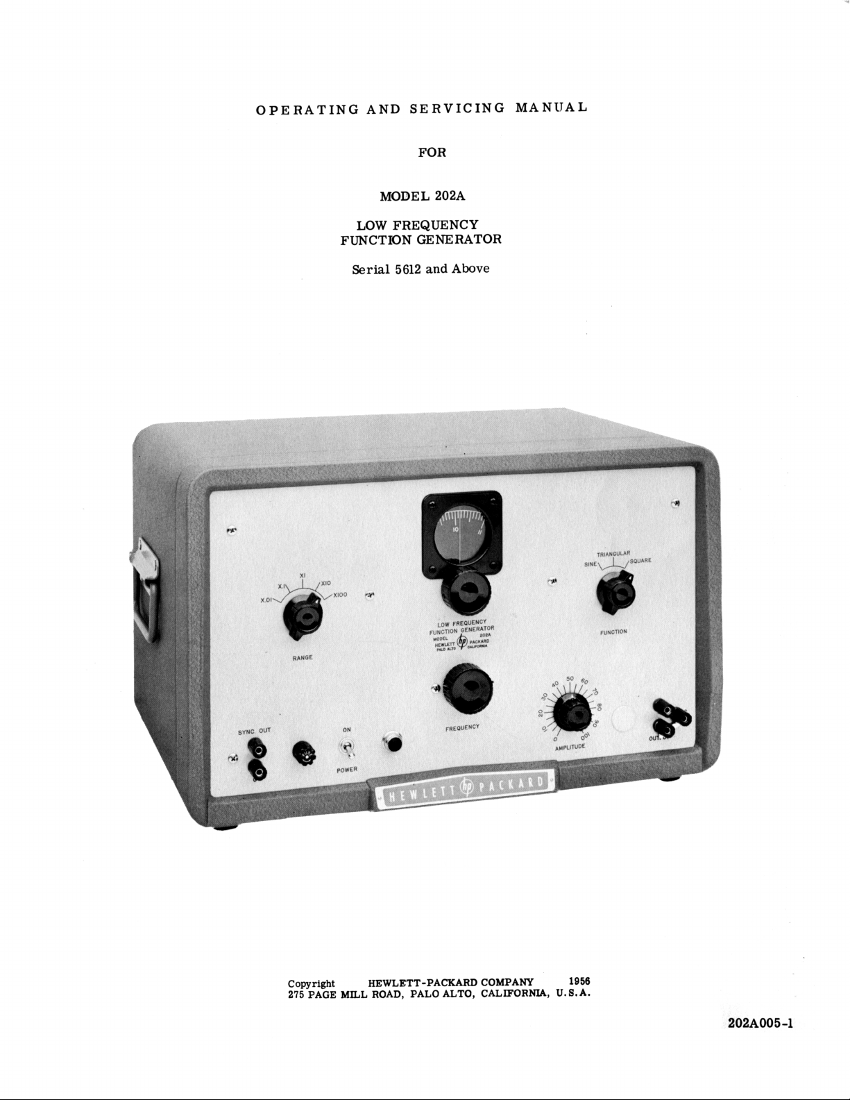
Page 1

Page 2
Page 3
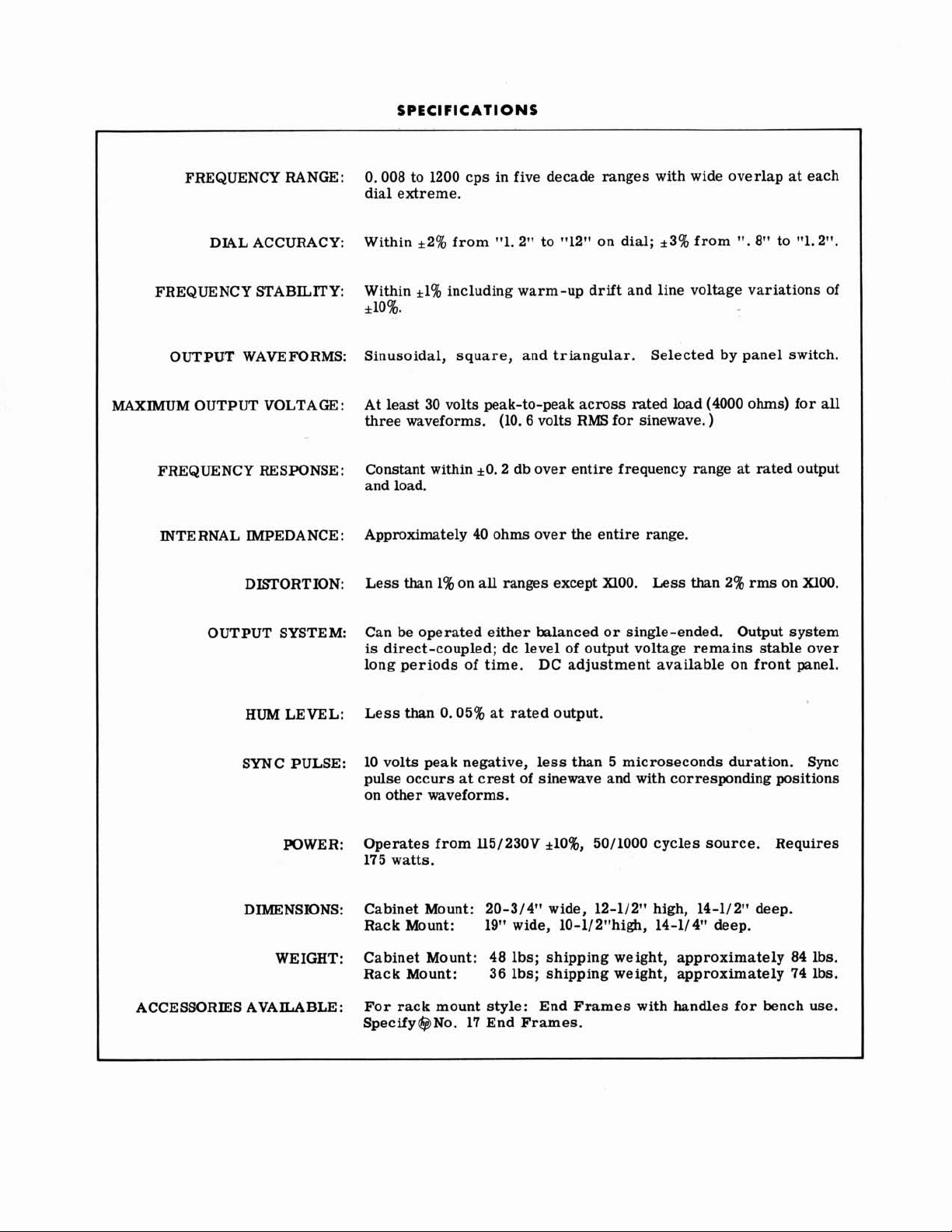
SPECIFICATIONS
r
FREQUENCY RANGE:
DIAL ACCURACY:
FREQUENCY STABILITY:
OUTPUT WAVEFORMS: Sinusoidal, square, and triangular. Selected by panel switch.
MAXIMUM OUTPUT VOLTAGE:
FREQUENCY RESPONSE:
lNTE RNAL IMPEDANCE
DISTORTION:
0.008 to 1200 cps in five decade ranges with wide overlap at each
dial extreme.
Within
Within
*lo%.
At least 30 volts peak-to-peak across rated load (4000 ohms) for
three waveforms. (10.6 volts RMS for sinewave.
Constant within
and load.
Approximately 40 ohms over the entire range.
:
Less than 1% on
*2% from "1. 2" to "121q on dial; *3% from ". 8" to "1.2".
4%
including warm-up drift and line voltage variations of
)
*0.2 db over entire frequency range at rated output
all
ranges except X100. Less than 2% rms on
all
X100.
OUTPUT SYSTEM:
HUM LEVEL:
SYNC PULSE
POWER: Operates from
DINENSIONS: Cabinet Mount: 20-314" wide, 12-112" high, 14-112" deep.
WEIGHT: Cabinet Mount: 48 lbs; shipping weight, approximately 84 lbs.
ACCESSORIES AVAILABLE:
Can
be
operated either balanced or single-ended. Output system
is
direct-coupled; dc level of output voltage remains stable over
long periods of time. DC adjustment available on front panel.
Less than
10 volts peak negative, less than 5 microseconds duration. Sync
:
pulse occurs at crest of
on other waveforms.
17 5 watts.
Rack Mount:
Rack Mount:
For rack mount style: End Frames with handles for bench use.
Specify
0.05%
@No. 17 End Frames.
at
rated output.
sinewave and with corresponding positions
ll51230V
19" wide,
36 lbs; shipping weight, approximately 74 lbs.
-+lo%,
10-l/21qhigh, 14-11 4" deep.
5011000 cycles source. Requires
Page 4
CONTENTS
SECTION I GENERAL DESCRIPTION Page
SECTION
SECTION
II
m
1 . 1
OPERATING INSTRUCTIONS
2
.
2
.
2 . 3 230-Volt Operation
2
.
2 . 5
.
2
.
2
THEORY OF OPERATION
3
-1
3 . 2 Bi-Stable Circuit
3 . 3 Linear Integrator
3
.
3 . 5
3
.
3-7 Powersupply
General
1 Inspection
2 Controls and Terminals .
4
Operation ..........
Single-Ended Output
6
Balanced Output
7
Sync Out 11-2
General
4
Sine Synthesizer and Function Selector Switch
Output System
6
Sync Pulse Output
...........
..........
.........
.
..........
...........
.........
.........
1-1
II . 1
II
.
11
II
II
II
III
III
III
III
III
III
III
.
.
.
.
......
.
\
.
........
........
.
.
........
1
1
1
2
2
SECTION IV MAINTENANCE
General
Power Supply
Function Generator (bi-stable circuit and integrator) .
Sine Synthesizer and Function Selector
Output Amplifier
sync Out
Tube Replacement
Tube Replacement Chart
Power Supply Regulator Adjustment
Theory of DC Balance and Distortion Adjustments
DC Balance and Distortion Adjustments . . .
Adjust Squarewave Amplitude .
Frequency Ratio and Calibration Procedure . . IV-8
Replacement of R58 Potentiometer .
SECTION
V
TABLE OF REPLACEABLE PARTS
5
.
1
Table
...........
.........
. IV
........
.......... IV
........
.
.
.
of
Replaceable
Parts
.
IV-1
IV
.
1
IV
.
2
.
2
IV
.
3
.
3
IV . 3
IV
.
4
N
.
4
IV
.
5
lV
.
5
IV
.
8
IV
.
9
V
.
1
Page 5
Sect. I Page 1
1-1
GENERAL
The Model 202A Low Frequency Function Generator
is
a compact, convenient, and versatile source of
transient-free test voltages between 1200 and
cycles per second. It
purpose low frequency testing application and
particularly valuable in the testing
geophysical equipment, vibration and stability characteristics of mechanical systems, electro-medical
equipment, and for the electrical simulation of
mechanical phenomena. Three types of output wave-
form are available; sine, square andtriangular.
Also, a sync output pulse
The Model 202A Low Frequency Function Generator
contains a type of relaxation oscillator that
ticularly advantageous for the generation of very low
frequencies. Both a triangular and
voltage function of time are inherent in the oscillating
system. Also, a
by synthesis from the triangular wave.
Output amplitude and distortion are virtually in-
dependent of the frequency of operation. This type
is
useful for any general
of
servo systems,
is
available for external use.
sinewave function
a
squarewave
is
.008
is
is
par-
produced
SECTION
GENERAL DESCRIPTION
of oscillating system in
plitude device so that no A.
sociated delay in stabilization after frequency changes,
is
required
The frequency range from
second
is
The output system
system designed for either single ended or balanced
output. It has good stability with respect to
current in the output and very low hum level. Both
the FUNCTION
control are so arranged that the characteristics of
the amplifier are independent of their position. The
internal impedance of the output amplifier
imately 40 ohms, and the unit
at least 30 volts peak-to-peak to a 4000 ohm load.
A negative peak sync pulse of 10 volts into a 2500
ohm load
than
sinewave and at corresponding positions with the
other functions.
is
covered in 5 bands. The frequency dial
linear.
selectro switch and the AMPLlTUDE
is
also provided.
5
microseconds and occurs at the crest of the
inherent^^
V.
.008 to 1200 cycles per
is
a direct-coupled amplifier
It
a constant am-
C. system, with as-
is
approx-
is
rated to deliver
has
a duration of less
direct
I
Page 6

Page 7
Sect.
I1
Page 1
2-1 INSPECTION
After the instrument
should be carefully inspected for damage received
If
in transit.
the procedure outlined in the "Claim for Damage in
Shipment" page at the back of the instruction book.
2-2
CONTROLS AND TERMINALS
any shipping damage
is
unpacked, the instrument
is
found, follow
RANGE
This switch
range to be covered
FUNCTION
This switch
types of output waveform.
FREQUENCY
This dial
for the
knob just below the dial escutcheon
nected to the frequency varying element. The lower
knob
is
of the frequency.
AMPLITUDE
This control adjusts the amplitude
voltage admitted
output
0 to 100 in arbitrary units.
from
is
used to select the desired frequency
by
the frequency dial.
is
used to select any one of the three
is
calibrated directly in cycles per second
X1 frequency range of the oscillator. The
is
directly con-
a
mechanical vernier for fine adjustment
of
the oscillator
to
the amplifier and, therefore,
of
.the instrument. This control
is
calibrated
the
SECTION
II
OPERATING INSTRUCTIONS
OUTPUT
This group consists of three terminals. The one
marked "G"
chassis.
are the OUTPUT terminals. With respect to the
ground terminal each of these outputs has equal
magnitude of signal, but they are 180" out of phase
with each other. The internal impedance between
the two OUTPUT
SYNC OUT
The Sync Out terminals are single-ended and have
an internal impedance of about 2,000 ohms.
Power Cable
The three-conductor power cable
a three-prong plug. The third prong
off -set pin which provides
adapter may be obtained to permit use of this plug
with two-conductor receptacles.
2-3 230-VOLT OPERATION
This instrument
the power transformer primaries connected in
parallel for
on
ified
primaries will have to be connected in series
shown in "Transformer Details" on the schematic
wiring diagram
is
connected directly to the instrument
The
other two terminals, vertically aligned,
115
v operation, unless otherwise spec-
the order.
terminals
is
If
of
the Power Supply Section.
is
appmximately
is
supplied with
a
chassis ground. An
shipped from the factory with
230 v operation
is
40
ohms.
is
a round
desired,
the
as
POWER
This toggle switch controls the power supplied to
the instrument from the power line.
FUSE
The fuseholder, which
tains the power line fuse. Refer to the Table
Replaceable
Parts
is
located on the panel, con-
for the correct fuse rating.
of
2-4 OPERATION
The following step-by-step procedure should
used
as
a
guide when operating this instrument.
1) Turn the POWER switch
seconds for oscillations to start. The instrument
will operate nearly within specifications after
few minutes warm-up.
30
cations after
minutes.
It
to
ON. Allow thirty
will
be within specifi-
be
a
Page 8
Sect.
I1
Page 2
2) Set the
desired frequency. The frequency dial scale must
be
multiplied by
the RANGE switch setting to obtain the oscillator
frequency. Example: 4 (on dial scale)
plying factor indicated by RANGE switch setting)
=
.4 cycles/sec.
3)
Set the FUNCTION switch for the desired output
waveform.
4)
Connect the equipment under test to the OUTPUT
terminals.
5) Adjust the AMPLITUDE Control for the desired
output voltage. Because the frequency response
is
rated k0.2 db, the output amplitude may
sured
level will be correct (within these limits) for any
other frequency.
RANGE
at
any convenient frequency and the output
and FREQUENCY controls for the
the
multiplying factor indicated by
x
.l
(multi-
be
NOTES
mea-
be
must
and the strapped pair will then be the ground side of
the output.
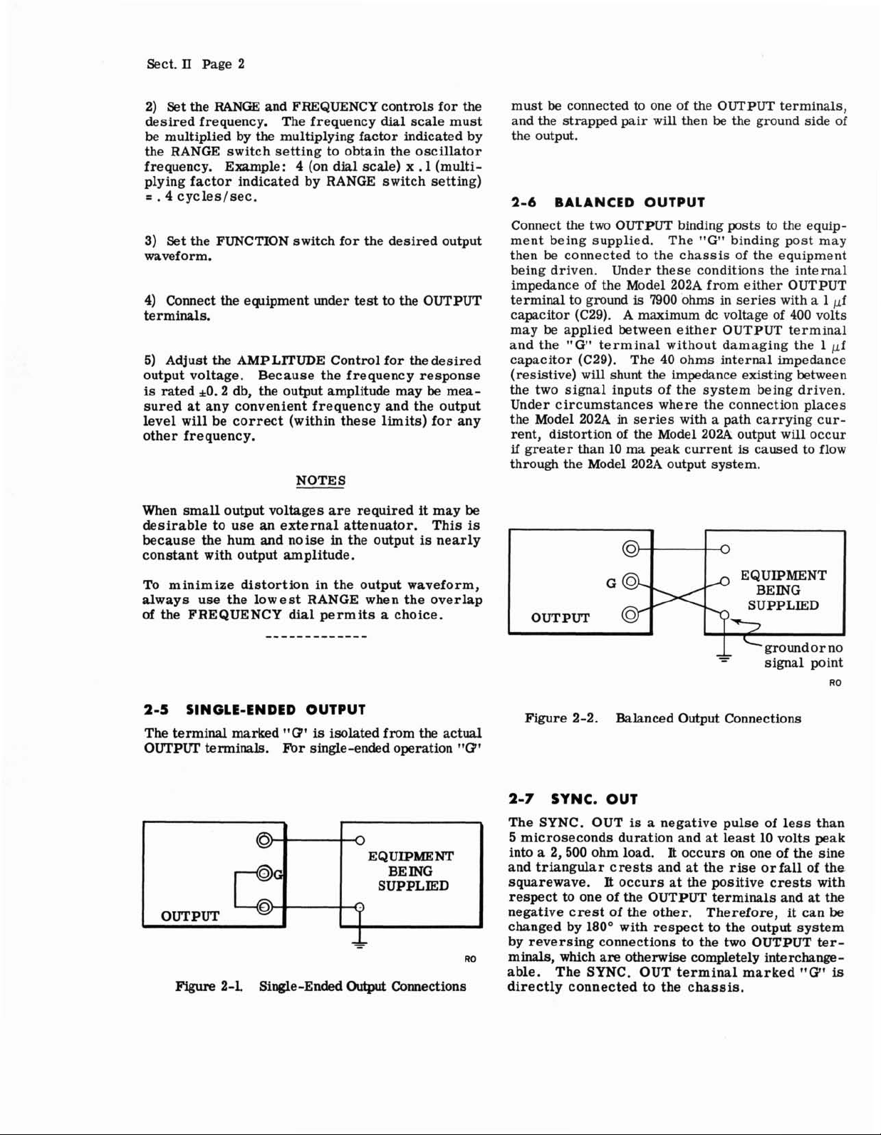
2-6
Connect the two OUTPUT binding posts
ment being supplied. The
then
being driven. Under these conditions the internal
impedance of the Model 202A from either OUTPUT
terminal to ground
capacitor (C29). A maximum dc voltage of 400 volts
may
and the
capacitor (C29). The 40 ohms internal impedance
(resistive) will shunt the impedance existing between
the two signal inputs of the system being driven.
Under circumstances where the connection places
the Model
rent, distortion of the Model
if
through the Model 202A output system.
connected
BALANCED
be
connected to the chassis of the equipment
be
applied between either OUTPUT terminal
"G" terminal without damaging the 1 pf
202A
greater than 10 ma peak current
to
one of the OUTPUT terminals,
OUTPUT
to
the equip-
"G" binding post may
is
7900 ohms in series with a 1 pf
in
series with a path carrying cur-
202A output will occur
is
caused to flow
When small output voltages are required it may
an
desirable to use
because the hum and noise
constant with output amplitude.
To
minimize distortion in the output waveform,
always use the lowest RANGE when the overlap
of
the FREQUENCY dial permits a choice.
external attenuator. This
in
the output
is
be
is
nearly
-------------
2-5
SINGLE-ENDED
The terminal
OUTPVT terminals. For single-ended operation
FYgwe
marked
2-L Single-Ended
"(3"
OUTPUT
is
isolated from the actual
0
EQUIPMENT
BEING
SUPPLIED squarewave.
-
-
Output
Co~ections directly connected to the chassis.
"(3'
RO
@
Figure 2-2. Balanced Output Connections
2-7
SYNC.
The SYNC. OUT
5 microseconds duration and
a
2,500 ohm load.
into
and triangular crests and at the rise
respect to one of the OUTPUT terminals and at the
negative crest of the other. Therefore,
changed by 180" with respect
by reversing connections to the two OUTPUT terminals, which are otherwise completely interchange-
able. The SYNC. OUT terminal marked
OUT
is
a negative pulse of less than
It
It
occurs at the positive crests with
0
EQUIPMENT
SUPPLIED
ground or no
-
at
occurs on one of the sine
to
signal point
least 10 volts peak
orfall of the
it
can
be
the output system
"G1'
is
Page 9
Sect.
111
Page
1
3-1
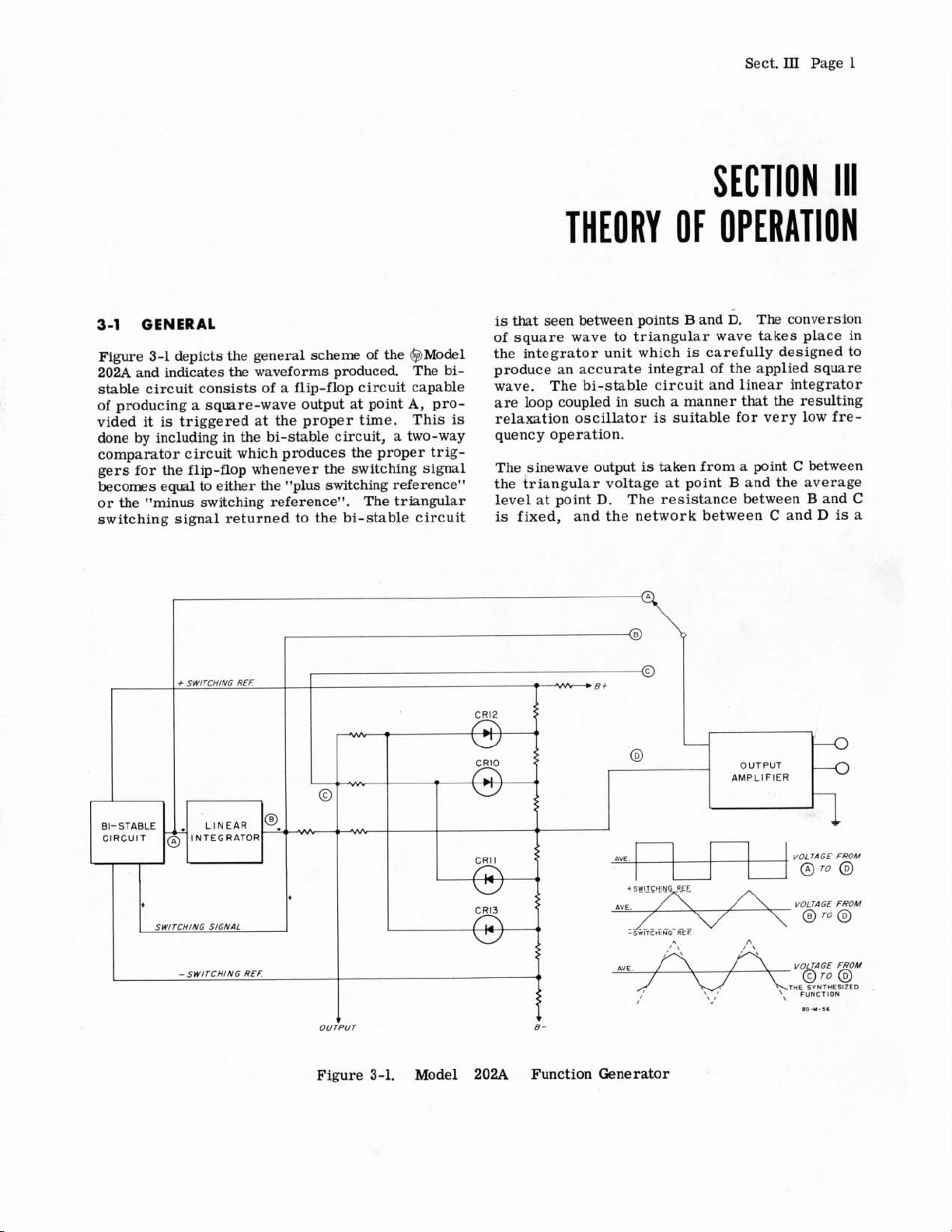
GENERAL
Figure 3-1 depicts the general scheme of the @Model
202A
and indicates the waveforms produced. The bistable circuit consists of a flip-flop circuit capable
of producing a square-wave output at point
vided
it
is
triggered at the proper time. This
done by including in the bi-stable circuit, a two-way
comparator circuit which produces the proper triggers for the flip-flop whenever the switching signal
becomes equal to either the
or the "minus switching reference". The triangular
switching signal returned to the bi-stable circuit
"plus switching reference"
A,
pro-
is
SECTION
Ill
THEORY OF OPERATION
is
that seen between points B and
of square wave to triangular wave takes place in
the integrator unit which
produce an accurate integral of the applied square
wave. The bi-stable circuit and linear integrator
are loop coupled in such a manner that the resulting
is
relaxation oscillator
quency operation.
sinewave output
The
the triangular voltage at point
level at point
is
fixed, and the network between C and
D.
suitable for very low fre-
is
taken from a point C between
The resistance between B and
D.
The conversion
is
carefully designed to
B
and the average
D
C
is
a
+
SWITCHING REF
+
SWITCHING SIGNAL
-SWITCHING REF
-
+
1
OUTPUT
Figure 3-1. Model
=
CR12
CRlO
CRIl
CR13
202A
-
8+
Function Generator
0
@
AVE
FtfH
,
-
OUTPUT
AMPLIFIER
vOLT4GE FROM
@TO
@
VOLTAGE FROM
, ,
Page 10
Sect.
III
Page
2
non-linear system which synthesizes a
sinewave
from the triangular wave. This network consists
of a group of biased diodes arranged in such a manner that at certain predetermined voltage levels they
begin to conduct, therefore, providing shunt paths
D.
from C to
Each additional shunt path reduces
the slope of the triangle in the proper amount so
that the wave
This approximation
which a
is
shaped to approximate a sinewave.
is
as shown, and the degree to
sinewave may be approached depends on
the number of diodes. Thus there are available
the
sinewave C, triangular wave B, and squarewave A functions with respect to D to be selected
and brought to the OUTPUT terminals through the
output amplifier. The output amplifier has a differ-
ential input and push-pull output.
3-2
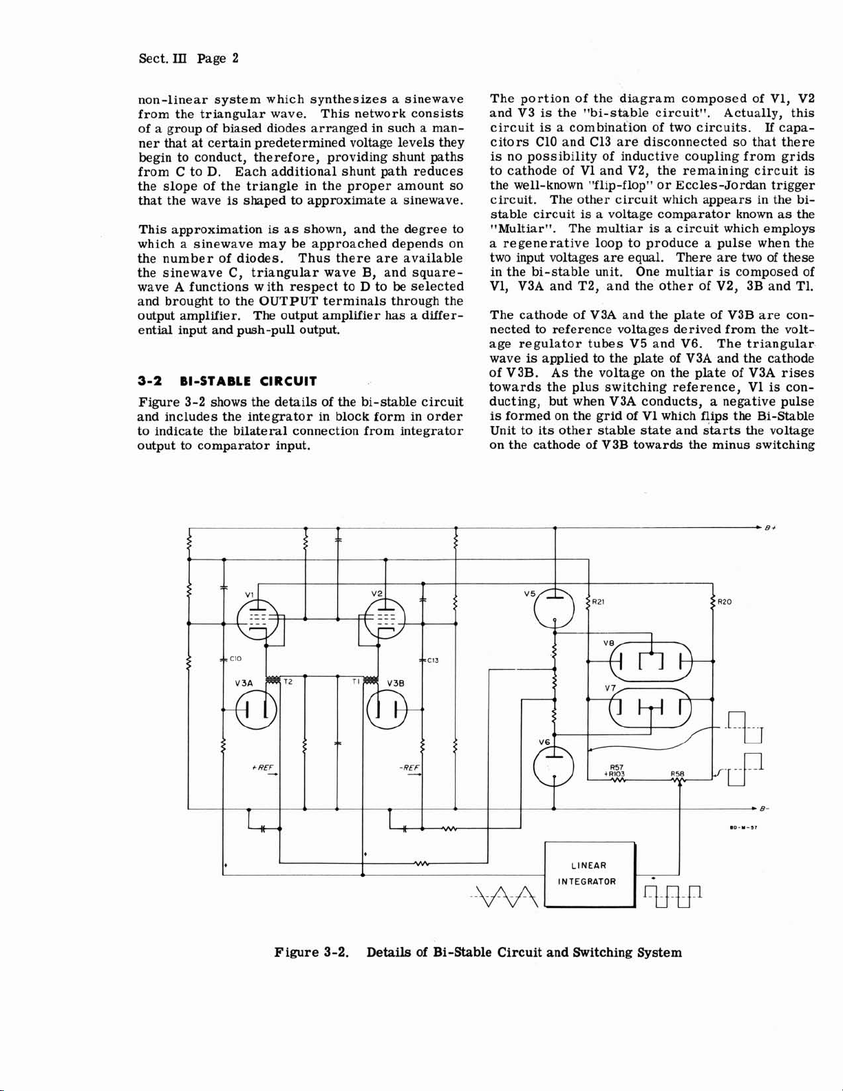
BI-STABLE CIRCUIT
Figure 3-2 shows the details of the bi-stable circuit
and includes the integrator in block form in order
to indicate the bilateral connection from integrator
output to comparator input.
The portion of the diagram composed of
V1, V2
and V3 is the "bi-stable circuit". Actually, this
circuit
citors
is
to cathode of
is
a combination of two circuits.
If
capa-
C10 and C13 are disconnected so that there
no possibility of inductive coupling from grids
V1 and V2, the remaining circuit
is
the well-known "flip-flop" or Eccles-Jordan trigger
circuit. The other circuit which appears in the bi-
is
stable circuit
"Multiar". The multiar
a voltage comparator known as the
is
a circuit which employs
a regenerative loop to produce a pulse when the
of
two input voltages are equal. There are two
is
in the bi-stable unit. One multiar
V3A and T2, and the other of V2, 3B and T1.
V1,
composed of
these
The cathode of V3A and the plate of V3B are connected to reference voltages derived from the voltage regulator tubes V5 and V6. The triangular.
is
wave
of
applied
V3B. As the voltage on the plate of V3A rises
towards the plus switching reference,
to
the plate of V3A and the cathode
V1
is
con-
ducting, but when V3A conducts, a negative pulse
is
formed on the grid of V1 which flips the Bi-Stable
Unit to its other stable state and starts the voltage
on the cathode of V3B towards the minus switching
Bf
-
$
4
I
SEC13
-
~'j1133!
V3B
IE
+REF
T
+
-
-REF
-
T
-
.-.
*
LINEAR
INTEGRATOR
R20
.0-"-,,
*
B-
Figure
3-2.
Details
of
Bi-Stable Circuit
and
Switching System
Page 11
reference. When V3B conducts the Bi-Stable Unit
is
flipped back to its original state, completing one
cycle of operation.
Voltage regulator tubes V5 and V6 are connected
by a voltage divider from which the switching reference voltages are taken. They also provide the
limiting voltages applied to tubes
V7 and V8 which
are seen to be a push-pull clamping system. Inasmuch as the integrator output
is
to the input, it
seen that the magnitude of square-
is
directly related
wave applied must be carefully controlled. Although only the squarewave appearing at the plate
of Vl
is
needed to drive the integrator, the clamp
is
made push-pull to prevent excessive current
variations in the regulator tubes. The action of
V7B and V8B
is
such that if the applied waveform
has peak excursions in excess of the potentials on
the remaining cathode and plate, these being deter-
by
mined
regulator tubes V5 and V6, a current will
flow through R20 which drops the voltage to very
nearly the potential of the regulated element of the
conducting section of the diode. The action of the
is
other diodes
the same, but 180" out of phase,
inasmuch as they are coupled to the plate of V2.
In
this way, waveforms appearing on the clamped
sides of R21 and
magnitude as well as
the average of dc level of the squarewave
R20 are assured to be of equal
180" out of phase, and further
is
ac-
curately controlled.
3-3
LINEAR INTEGRATOR
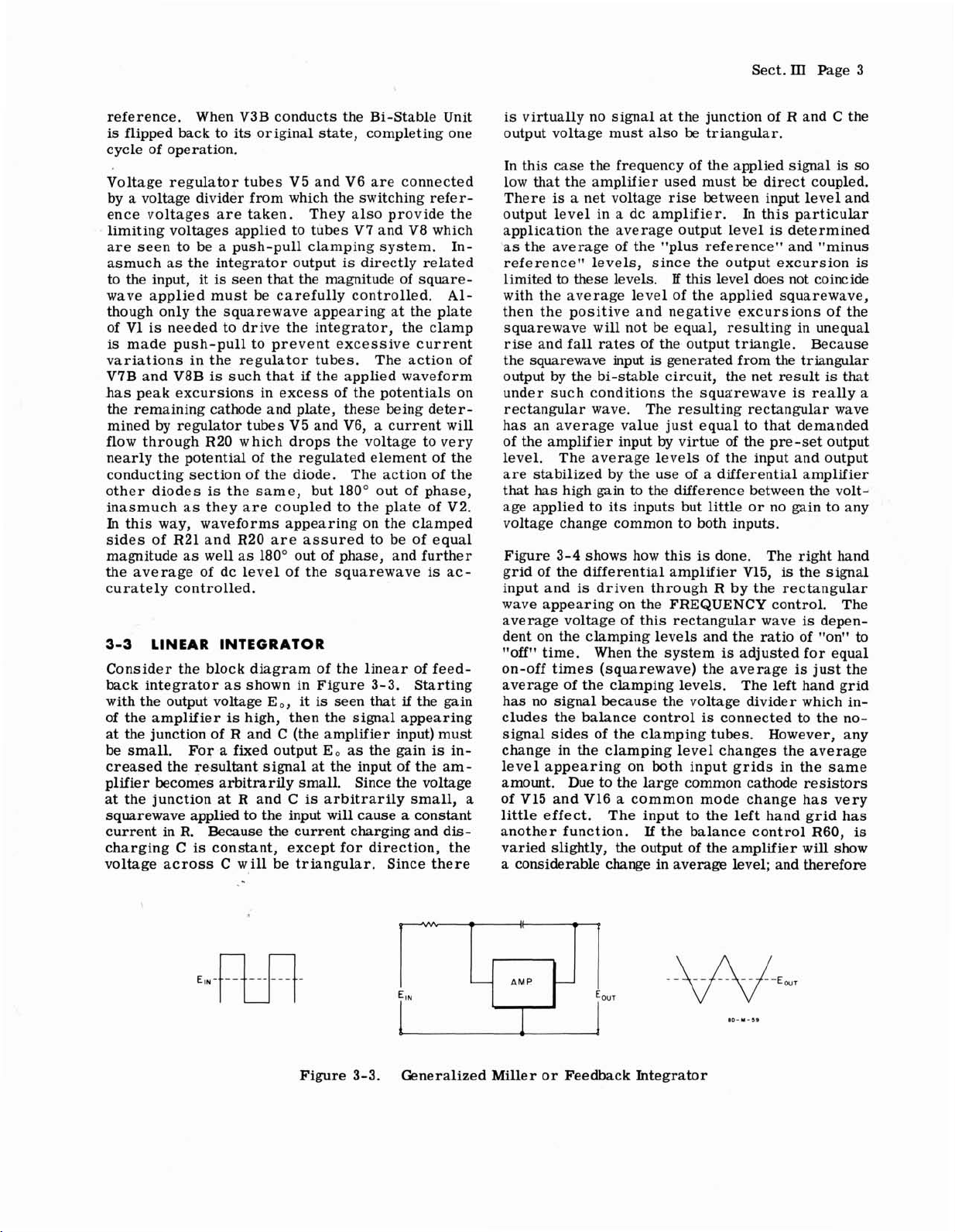
Consider the block diagram of the linear of feedback integrator as shown in Figure 3-3. Starting
with the output voltage
of the amplifier
at the junction of R and
be
small. For a fixed output Eo as the gain
E,,
it
is
seen that
is
high, then the signal appearing
C
(the amplifier input) must
if
the gain
is
in-
creased the resultant signal at the input of the am-
plifier becomes arbitrarily small. Since the voltage
C
is
at the junction at R and
arbitrarily small, a
squarewave applied to the input will cause a constant
current in R. Because the current charging and dis-
charging C
is
constant, except for direction, the
voltage across C will be triangular. Since there
Sect.
III
Page 3
is
virtually no signal at the junction of R and C the
output voltage must also be triangular.
In this case the frequency of the applied
signal
is
so
low that the amplifier used must be direct coupled.
is
There
a net voltage rise between input level and
output level in a dc amplifier. In this particular
application the average output level
is
determined
as the average of the "plus reference" and "minus
reference" levels, since the output excursion
limited to these levels.
B
this
level does not coincide
is
with the average level of the applied squarewave,
then the positive and negative excursions of the
squarewave will not be equal,
resulting in unequal
rise and fall rates of the output triangle. Because
squarewave input
the
is
generated from the triangular
output by the bi-stable circuit, the net result is that
is
under such conditions the squarewave
really a
rectangular wave. The resulting rectangular wave
has an average value just equal to that demanded
by
of the amplifier input
virtue of the pre-set output
level. The average levels of the input and output
are stabilized by the use of a differential amplifier
that has high gain to the difference between the voltage applied to its inputs but little or no gain to any
voltage change common to both inputs.
is
Figure 3-4 shows how this
grid of the differential amplifier
is
input and
driven through R by the rectangular
wave appearing on the FREQUENCY control.
average voltage of this rectangular wave
done.
The right hand
V15,
is
the signal
is
The
depen-
dent on the clamping levels and the ratio of "on" to
is
"off" time. When the system
on-off times (squarewave) the average
adjusted for equal
is
just the
average of the clamping levels. The left hand grid
has no signal because the voltage divider which in-
is
cludes the balance control
connected to the nosignal sides of the clamping tubes. However, any
change in the clamping level changes the average
level appearing on both input grids in the same
amount. Due to the large common cathode resistors
of V15 and V16 a common mode change has very
little effect. The input to the left hand grid has
another function.
If
the balance control R60,
is
varied slightly, the output of the amplifier will show
a
considerable change in average level; and therefore
-
€9,
t
-
-
AMP
-
-
Eour
a
Figure 3-3. Generalized Miller or Feedback Integrator
ID-"-5.
Page 12
Sect.
III
Page
4
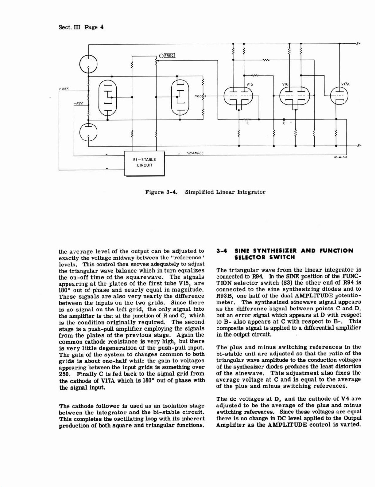
Figure 3-4. Simplified Linear Integrator
the average level of the output can be adjusted to
exactly the voltage midway between the "reference"
This
levels.
control then serves adequately to adjust
the triangular wave balance which in turn equalizes
the on-off time of the squarewave.
The signals
appearing at the plates of the first tube V15, are
180" out of phase and nearly equal in magnitude.
These signals are also very nearly the difference
between the inputs on the two grids. Since there
is
no signal on the left grid, the only signal into
is
the amplifier
is
the condition originally required. The second
is
stage
a push-pull amplifier employing the signals
that at
the
junction
of
R and C, which
from the plates of the previous stage. Again the
common cathode resistance
is
very little degeneration of the push-pull input.
is
very high, but there
The gain of the system to changes common to both
is
grids
appearing between the input grids
250. Finally C
the cathode
about one-half while the gain to voltages
is
something over
is
fed back to the signal grid from
of
V17A which
is
180" out of phase with
the signal input.
is
The cathode follower
used as an isolation stage
between the integrator and the bi-stable circuit.
This completes
oscillating loop with
its
inherent
the
production of both square and triangular functions.
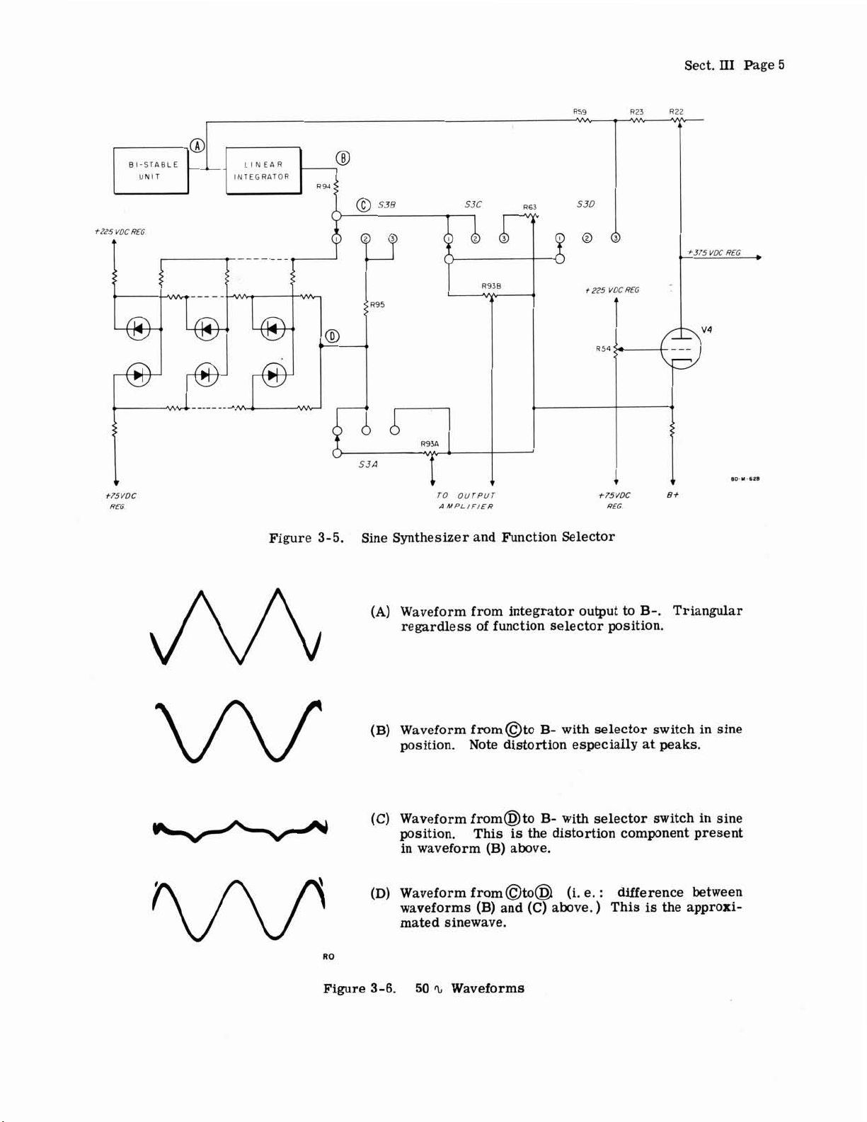
3-4
The triangular wave from the linear integrator
connected
TION selector switch (53) the other end of R94
connected to the sine synthesizing diodes and
R93B, one half of the dual
meter. The synthesized
as the difference signal between points C and
SINE SYNTHESIZER AND FUNCTION
SELECT OR
to
R94.
SWITCH
In
the
SINE position
AMPLITUDE
of
the
FUNC.-
potentio-
sinewave signal appears
D,
is
is
to
but an error signal which appears at D with respect
to
B-
also appears at C with respect to
composite signal
is
applied
to
a differential amplifier
B-.
This
in the output circuit.
The plus and minus switching references in the
bi-stable unit are adjusted so that the ratio of the
triangular wave amplitude to the conduction voltages
the
synthesizer diodes produces
of
the
least distortion
of the sinewave. This adjustment also fixes the
is
equal
to
average voltage at C and
the average
of the plus and minus switching references.
at
The dc voltages
D, and the cathode of V4 are
adjusted to be the average of the plus and minus
switching references. Since
there
is
no change in DC level applied to the Output
as
Amplifier
the AMPLITUDE control
these
voltages are equal
is
varied.
Page 13
El-STABLE
f
225
VDCREG
.
Sect.
111
Page 5
t75
VDC
REG AMPLIFIER
Figure 3-5.
Sine Synthesizer and Function Selector
(A)
TO OUTPUT
Waveform from integrator output to B-. Triangular
regardless of function selector position.
(B) Waveform from@to B- with selector switch in sine
position. Note distortion especially at peaks.
w
(C) Waveform from@to B- with selector switch in sine
position.
in waveform (B) above.
This
t75
VDC
REG.
is
the distortion component present
ID.I.6M
RO
Figure
(D) Waveform fromato@ (i. e.
(C)
waveforms (B) and
above. ) This
mated sinewave.
3-6.
50
IL
Waveforms
:
difference between
is
the approxi-
Page 14
Sect.
111
Page 6
sinewave
The
resistance across
is
approximated by varying the shunt
R93B
is
steps determined by the
diode synthesizing network. The waveform slope,
is
at first,
just that determined by R94, R93B and
the input waveform. When the first diode conducts
is
R93
shunted by a predetermined amount, decreasing the slope. Each diode in turn decreases the
slope until all the diodes are conducting and the
triangular wave
has
reached
its
crest. The triangular
wave starts down, the diodes stop conducting in turn
until the triangular wave has reached its crest. The
triangular wave
starts
down, the diodes stop conduct-
ing in turn until the triangular wave reaches the
average level. The other half-cycle is formed in
the same manner, but by the diodes that are biased
to shape the negative excursion.
It can
be
shown that using seven segments to approx-
imate one half cycle of the
sinewave results in ap-
proximately 11 6% rms distortion. However, variations
in the diodes limit the practical result to about
1%
rms distortion.
In
the triangular wave position of the FUNCTION
selector switch the non-linear load consisting of
is
the diode network
combination R94 and R95
for all voltage levels. It
replaced by R95 so that the
is
a simple linear divider
is
adjusted to give equal
sine and triangular wave peak magnitude.
is
squarewave
connected to the FUNCTION selector
The
switch through the divider R59 and R22 which adjusts
the average voltage of the squarewave to the voltage
at the cathode of V4. In the squarewave position
of the selector switch, R63 parallels
R93B to adjust
the amplitude of the squarewave to be equal to the
amplitude of the
3-5
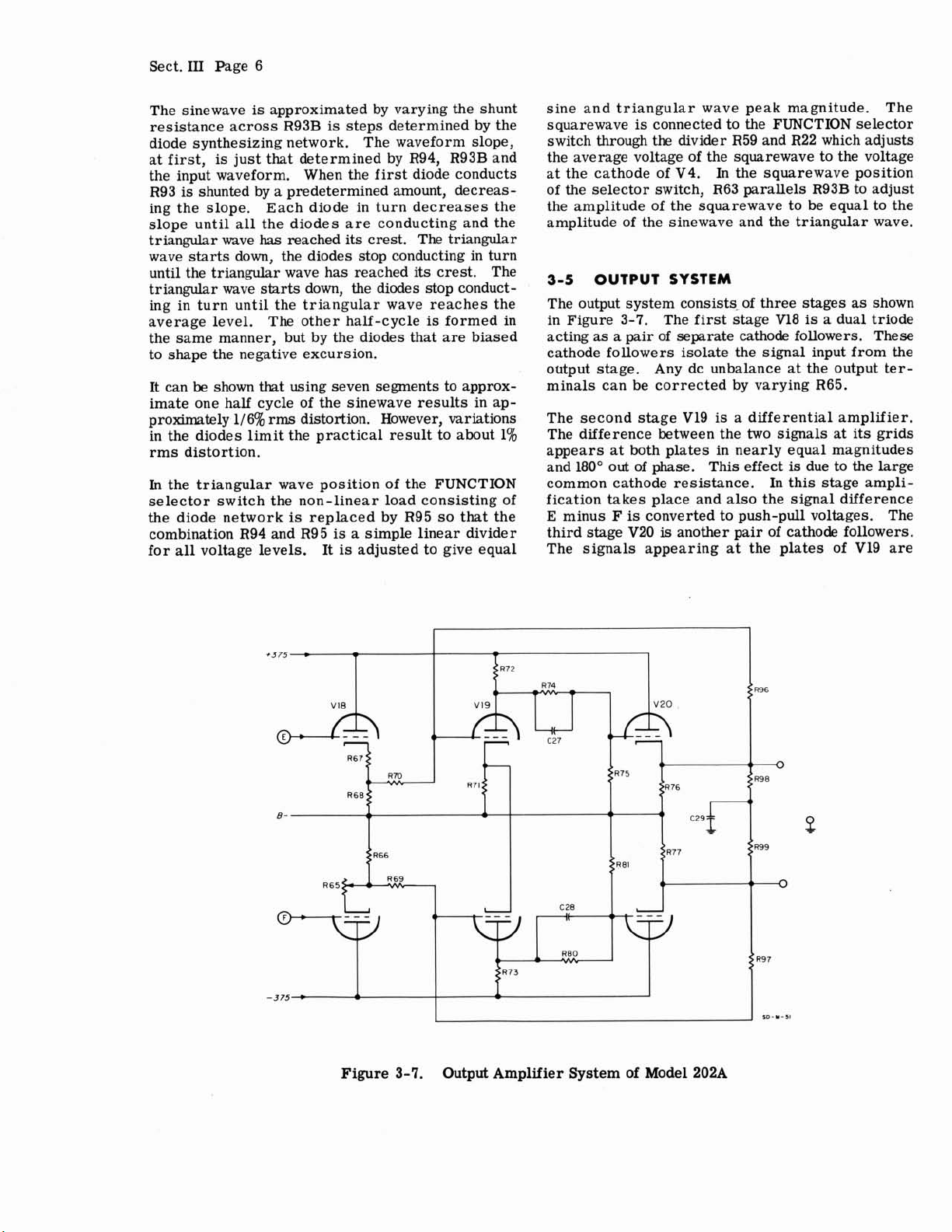
OUTPUT
sinewave and the triangular wave.
SYSTEM
The output system consists of three stages as shown
in Figure 3-7. The first Stage V18
acting
as
a pair of separate cathode followers.
is
a dual triode
These
cathode followers isolate the signal input from the
output stage. Any dc unbalance at the output terminals can be corrected by varying R65.
The second stage
V19
is
a differential amplifier.
The difference between the two signals at its grids
appears at both plates in nearly equal magnitudes
is
and 180" out of phase. This effect
due to the large
common cathode resistance. In this stage ampli-
fication takes place and also the signal difference
E
minus F
third stage V20
The signals appearing at the plates of
is
converted to push-pull voltages. The
is
another pair of cathode followers.
V19 are
Figure
3-7.
Output Amplifier System of Model
202A
Page 15

Sect.
111
Page
7
R44 R41
Sync Output Circuit of Model 202A
attenuated before being applied to
Figure 3-8.
the
cathode follower
grids. The small shunt capacitors on the upper sides
of the dividers improve the high frequency response
of the amplifier. The voltages appearing at the
cathode follower output terminals are equal in magnitude and
180" out of phase. Negative feedback
is
used to reduce distortion, lower the output impedance
and improve stability. This improved stability
applies not only to the signal output, but to the dc
level at the output terminals.
The symbol for chassis or ground
first time in the output terminal network R98,
and C29.
for operation has been
the
Thus, the chassis ground
B-
In
all other description the reference level
B-,
and in the Model 202A
line
is
completely isolated from the chassis.
is
available for whatever
is
used for the
R99
CZO
is
possible to consider
connection
is
desired.
It
the two output terminals as a transformer output
and further to balance this apparent transformer to
chassis by making R98 equal to
R99. The capacitor
C29 insulates the apparent transformer secondary
from ground.
If
single-ended operation
is
desired
the ground connection can be tied to either output
terminal without affecting the amplifier.
3-6
The output sync pulse
circuit
SYNC PULSE OUTPUT
is
obtained from the bi-stable
V1
and V2.
On
the minus switching reference
at the plate of multiar diode V3, one positive pulse
and one negative pulse appear for every cycle of
operation. These pulses are coupled to the grid
FlER
REGULATOR
Figure 3-9. Model 202A Power Supply
f
375
VOLTS
REG
.-0
-
+P25
VOLTS
rs
REG
REG
Page 16

Sect.
111
Page
8
of the sync pulse amplifier, V17, through an
coupling which lowers the average voltage on the
In
grid to B-.
to cut-off by the bleeder to B+. When a positive
pulse appears at the grid, it momentarily turns
V17 "on", thus, inducing a large voltage swing in
the pulse transformer primary. The resistor and
diode in the secondary remove the positive excursion,
resulting in a negative pulse at the
minals.
the absence of pulses, V17
SYNC OUT
is
biased
RC
ter-
3-7
The Power Supply
tor which supplies
+
divider across the + 375 volt supply. The main
requirement on the three regulated voltages
low impedance at low frequencies. Reasonable variations in the actual voltages do not affect the output
frequency or waveform.
POWER
225
volt regulated outputs are taken from a voltagc
SUPPLY
is
a full wave rectifier and regula-
+
375 volts. The + 75 volt and
is
very
Page 17

Sect.
IV
Page 1
4-1
GENERAL
Most of the following analyzing and adjustment procedures require the measurement of dc voltages or
the observation of waveforms. To obtain accurate
results, use a voltmeter with an input resistance of
100 megohms or more. The @Model 410B Vacuum
Tube Voltmeter
All dc voltages are measured with respect to B- and
not with respect to the chassis. The B- points in
the instrument are connected with
Isolate all test equipment from the main chassis or
gromd Otherwise, both
may be connected to the main chassis through the
test equipment.
in output stage V20 will be shorted and the tube will
be
severely damaged.
is
recommended.
black
hook-up
CAUTION
B-
and one side
I€
this happens, one cathode resistor
of
wire.
the output
--------------
SECTION
IV
MAINTENANCE
4-2
POWER SUPPLY
After power
ments, a final check of regulated voltages should
be
made. See Power Supply Regulator Adjustments
in paragraph 4-9.
SYMPTOM
Instrkent inoperative
(Indicator lamp won't
light, no output volt-
age).
Instrument inoperative
(Indicator lamp lights,
no output voltage).
supply parts replacements or adjust-
TABLE 4-1
CAUSE AND/OR
REMEDY
Blown fuse,
Measure resistance
from V21 socket
(pins 2 or
55,000 ohms or
more replace
If
less than 55,000
ohms clear short
circuit in filter or
regulator circuits
then replace V21.
8)
F1.
to B-.
V21.
1
Whenever pssible the instrument frequency should
be set to approximately 50
the use of a capacitor in series with the ac voltmeter
or oscilloscope to eliminate the dc component.
Interaction between most of the circuits of the Model
202A makes a fairly definite procedure for trouble
shooting necessary. For example,
oscillator section may easily cause considerable
voltage deviations in the output system. Therefore,
is
more desirable to divide the instrument into
it
five sections as follows and consider each in turn.
4-2 Power Supply
4-3 Function Generator
Sine Synthesizer and Function Selector
4-4
4- 5 Output Amplifier
4-6 Sync Out
cycles/sec. to permit
a
fault in the
Instrument inoperative
(normalvoltage
(Extremely low or no
voltage between Y5,
pin 5 and B-).
Instrument inoperative
(normal
ulated) (+225V regulated, off voltage).
(+
7W regulated, off
voltage)
Instrument inoperative
(No
+
75 regulated voltages,
V5
ionized).
+
+
225 regulated
and/or V6 not
atV21).
37W reg-
Defective
tubes (V22, V23).
Capacitor C6 short
circuited.
Defective OA2 tube
(V5).
Defective OA3
(V6).
Open circuit in R62,
R84, R85,
R92.
6AU5
tube
R91, or
Page 18

Sect.
lV
Page 2
4-3
FUNCTION GENERATOR
(bi-stable circuit and integrator)
REPAIR ANALYSIS OF FUNCTION
A.
me
voltage, then a simple test should be made to deter-
is
mine whether the fault
bi-stable circuit.
1) Connect a high resistance dc voltmeter between
B- and pin 3 of tube
Set the
2)
connect the lead from the center lug of the variable
resistor R58. Temporarily connect this lead to
pin 5, V6
3) After this connection
cated by the voltmeter should slowly climb until
is
over 200 volts.
4) Remove the lead from the + 75 Reg. supply and
connect
meter indication should now drop slowly
140 volts. Disconnect the lead from V5 and return
it to the original connection on R58.
5)
If
quirements, then the integrator section
normally and the fault
circuit.
then the trouble
After all defective parts have been replaced and
the necessary adjustments made, an oscilloscope
should be connected between pin 3, tube
B- to see
on all ranges.
No output voltage (Power
Supply Section normal,
no triangle voltage between
on any range).
Same symptoms as above
on one or more ranges.
RANa switch to the
(+
it
to pin 2, V5 (+225 regulated). The volt-
the instrument meets the above voltage re-
If
the instrument does not pass the test,
if
a good triangular waveform
SYMPTOM
V17, pin 3 and B-
This test
75 Reg.
is
in the integrator.
in the integrator or the
is
V17.
X.
).
is
made, the voltage indi-
is
confined to the bi-stable
,
TABLE 4-2.
a
GE3lERATOR
as follows:
01 position. Dis-
to
less than
is
functioning
V17 and
is
obtained
CAUSE
Replace
V3, Vl5, V16,
or
replacement fails
to cure the trouble,
see analysis procedure following
this
Check RANGE
switch contacts,
components, and
connections.
Check C14-C18
for excessive
leakage.
AND/OR
REMEDY
V1,
V17.
If
chart.
V2,
tube
7
it
4-4
SYMPTOM
Same symptoms as
above when frequency
is
dial
frequency end.
Triangle not linear.
SINE SYNTHESIZER _AND FUNCTION
SELECTOR
When the trouble has been corrected in the Sine
Synthesizer and Function Selector, the following
checks should
is
ment
1) Sine Wave
V18 and B- with oscillator set to 50
the AMPLITUDE control at maximum. Set the
FUNCTION switch in the SINE position. The waveform should
imately 30 volts peak-to-peak. See Figure 3-6B.
Observe the waveform between pin 7, V18 and Bwith the same conditions as above. The waveform
should be similar to Figure 3-6C and approximately
1 volt peak-to-peak.
2) Triangular Wave
tween Pin 2, V18 and B- with the oscillator set
50 cycles/sec. and the AMPLITUDE control at
imum Set
position. The waveform should be triangular and
approximately 30 volts peak-to-peak.
Observe
same conditions as above. The waveform should be
triangular and approximately
3) Square Wave
pin 7, V18 and
sec. and the AMPLITUDE control
Set the FUNCTION switch to the SQUARE position.
The waveform should be square and approximately
30 volts peak-to-peak.
The
be adjustable to zero under any operating conditions
by means of R65.
again functioning correctly.
the
dc voltage across the
TABLE 4-2. (CONT'D)
CAUSE
Try replacement
tubes for V15, V16,
set near low
be
made to determine
-
Observe the waveform between pin 2,
be
substantially sinusoidal and approx-
-
the
FUNCTION switch in the TRIANGULAR
waveform between pin 7, V18 and
-
Observe the waveform between
B-
with the oscillator set to
and/or
Replace tubes V15,
V16, V17. Check
-
DC Balance.
Observe the waveform be-
1
volt peak-to-peak.
AND/OR
REMEDY
V17.
if
cycles/sec. and
at
OUTPUT
terminals should
the instru-
to
max-
B-
with
50
cycles1
maximum.
Page 19

Sect.
IV
Rage 3
TABLE 4-3.
SYMPTOMS
Sinewave badly
distorted.
DC component at OUTPUT terminals independent of AMPLITUDE
control setting or varied
by AMPLITUDE control.
4-5 OUTPUT AMPLIFIER
TABLE 4-4.
SYMPTOMS
CAUSE AND/OR
REMEDY
Maladjustment of
R49, R51, and
R6O
or defective diodes
CR2 through
CR13.
Maladjustment of
R65, R54, and R118
or defective tubes
V4, V18,
V19, V20.
See DC Balance
Adjustment.
CAUSE AND/OR
REMEDY
After adjustment or tube replacement, the amplifier
.I
should meet the following specifications:
---
The output voltage should not drop more than
2%
when a 4000 ohm load
is
connected to the
output.
---
The distortion should remain within specifi-
is
cations when the output
loaded with 4000 ohms
or higher.
---
The peak-to-peak output voltage should be at
least 30 volts (10. 6 volts rms with a sinewave)
is
when the output
loaded with 4000 ohms or
higher.
4-6
SYNC OUT
Specifications call for a negative sync pulse of 10
volts peak with a duration less than 5 microseconds.
The sync pulse occurs at the
>
sinewave crest and
at corresponding positions on other waveforms.
Increased distortion
when amplifier
is
loaded with 4000 ohms.
DC voltage component
exists across the OUT-
PUT terminals.
Distortion increases
appreciably with reduced AMPLITUDE
control setting.
Failure to deliver 10
volts rms
sinewave
output.
Hum in output voltage.
Replace
V20.
Vl8, Vl9,
If
distortion
remains, turn off
the power and mea-
sure resistance be-
tween internal
chassis and main
chassis. See paragraph 4-9.
See paragraph 4-4.
Replace variable
resistor
R93A,
R9 3B.
Adjust regulated
&
voltage. See para-
graph 4-9.
Replace
Vl8, Vl9,
v20.
Excessive hum from
power
supply See
paragraph 4-9.
TABLE 4-5.
CAUSE AND/OR
SYMPTOMS
No sync pulse (Check
REMEDY
Replace
Vl7.
for negative pulse
with oscilloscope and
with Mode1 202A set
for highest frequency).
Large overshoot.
,
4-7
TUBE REPLACEMENT
Replace CR1.
Any tube with standard JETEC characteristics can
be used for replacement purposes.
Whenever a tube
strument which might be affected
must be tested and
is
replaced, that part of the in-
by
the change
if
necessary, adjusted to be
within specifications. See paragraph 4-8, Tube
Replacement Chart.
Page 20

Sect.
lV
Page 4
4-8
TUBE REPLACEMENT CHART
TABLE 4-6.
TUBE
Vl, V2
V3
V4
V5, V6
V7, V8
Vl6, V17
V15,
Vl8, Vl9, V20
EFFECT
None. Variations in bottoming
voltage eliminated by clamps
and V8.
Frequency shift and distortion
increase due to contact potential
variations.
DC output level shift, probably
as a function of amplitude control setting.
Possible change in frequency,
distortion, or dc balance from
change in regulated voltages.
Same effect as change in V3
possible, but to much less
degree.
Frequency change and unbalance
of triangle.
Change in dc output component,
independent of AMPLITUDE
control setting.
V7
READJUSTMENT
None.
Min. Distortion and Correct
Freq. Adj.
DC Bal. Adj.
Power Supply.
Bal Adjust.
DC
Minimum Distortion and
Correct Freq. Adjust.
Min. Distortion and Correct
Freq. Adj.
Min. Distortion and Correct
Freq. Adj.
Set dc output component to
zero by R65, with amplitude
control min.
V21
V22, V23, V24, V25
4-9
POWER SUPPLY REGULATOR
ADJUSTMENT
Resistance measured between inner and outer chassis
should be at least two
minals disconnected from panel ground or a load.
This resistance check should be
the following adjustment procedure:
1) Connect the shorting strap between the lower
output terminal and chassis ground. Connect the dc
voltmeter between
voltmeter must not be grounded and the common
terminal should
megohms with OUTPUT ter-
B-
and the inner chassis. The
be
connected to
No effect
Possible change in
+
225 regulated voltages.
made
before starting
B-.
None.
+
375 and
2) Connect the 202A
The voltmeter indication should be between
+
230 volts with line voltage set to 115 volts.
and
3) Measure the regulated output voltage between
B-
and pin 2 of
a voltage of
4)
Measure the voltage between pin 5 of tube V5 and
B-.
This voltage should be about + 375 volts. Variations in OA3 tubes can cause this voltage
low
as
+
365 or as high
Carry out procedure under
"Power Supply Regulator
Adjustment". Paragraph
4-9.
to
the power line and turn on.
tube
V5. Adjust control R11 to give
225 volts.
as
393.
to
/
be
+
.
190
as
Page 21

Sect.
IV
Page
5
5) Measure the voltage between pin 5 of tube V6
B-.
and
Variations in OA3 tubes can cause this voltage to
fall at any point between 68 and 85 volts.
6) Repeat step 3
The characteristics of cold-cathode regulator tubes
drift during about the
This drift can affect the 202A output. A 72 hour
aging
V5 or V6.
7) Test the regulated output voltage at pin 5 of tube
V5 while varying line voltage between 103 and 127
volts. The regulated voltage
by more than
components if the change
4-10 THEORY OF DC BALANCE AND
The output AMPLITUDE control
input to the output amplifier.
at the output terminals
of the AMPLITUDE control the dc levels at the ends
of
the AMPLITUDE control must be the same and
also equal to the average level of the input wave.
From the schematic wiring diagram,
the common connection between the two sections of
the control
level of this point
by R54. The signal impedance of this point
low compared with the magnitude of the AMPLITUDE
control impedance, and therefore, the cathode of
has
V4
When R49, R51, R54, and R60 are adjusted properly,
there
the AMPLITUDE control.
When the FUNCTION switch
position, there
the AMPLITUDE control, hence, the tap on that
section merely carries the constant bias level set
by the cathode
through a network to the clamp section of the bi-
stable circuit. R22
age level
control to the same value as the cathode
The dc levels at
pendent of AMPLITUDE control setting. The dc
levels of the two output terminals may
to
be
of the signal on one grid of the second stage of the
amplifier. When these adjustments are made, the
dc component between the output terminals will
remain at a very low value, independent
setting or waveform selected.
This voltage should be about + 7 5 volts.
if
you replace either V5 or V6.
first
72 hours of operation.
is
recommended for a new tube for either
will
normally not change
*l%.
Check power supply tubes and
is
excessive.
DISTORTION ADJUSTMENTS
is
located at the
If
the dc component
is
to be zero for all settings
it
is
is
connected to the cathode of V4. The
can
be adjusted to the desired value
virtually zero signal.
is
no dc component across either section
is
in the squarewave
is
no signal input to one section
of
V4. The other section
d
this network adjusts the aver-
of
the squarewave applied
is
connected
to
the amplitude
of
the
input to the amplifier are inde-
be
equal
by
R65. Control R65 varies the dc level
of
amplitude
seen that
is
very
of
of
V4.
adjusted
Control R49 varies the level to which the output of
a
the integrator rises in
varies the level
levels of the shaper diodes are not variable and
therefore, the triangle input
one and only one correct magnitude and average
level.
Figure 4-2 shows the situation at the shaper when
the two reference levels are properly adjusted.
Figure 4-2B shows the effect of having the reference
levels adjusted for too large a magnitude, but with
the proper average value. Figure 4-2C shows the
effect of having reference levels adjusted for a
triangle of the proper magnitude, but incorrect
average level. This indicates
between correct frequency calibration and minimum
distortion. In fact, the two conditions are simultaneously satisfied by optimum settings of the same
adjustments.
4-11 DC BALANCE AND DISTORTION
ADJUSTMENTS
The following test procedure re@ires a
with an input resistance of at least 100 megohms
such as an
meter must not
the meter must
202A
that
Analyzer and an Oscilloscope will also be required.
A 20 minute warm-up
start
this procedure. You should also adjust the
power supply
1) Adjust the insulated 410B voltmeter to indicate
0.5 on the
Use either the
ECTOR switch
0.
5
setting
indication will be called
portion of this procedure.
2) Connect the
to the common junction of AMPLITUDE controls
R93A and R93B (violet wire).
3) Connect the DC volts probe
of
R93A. This
PLITUDE control.
4) Set the FUNCTION switch to TRIANGULAR and
adjust R54 for
5) Move the DC volts probe to the arm of Rl18 and
adjust R118 for an indication of approximately
volts".
of
the negative excursion. The b6s
@Model 410B. In addition, the volt
be
be
are not at ground potential. A Distortion
as
outlined in paragraph 4-9.
1
volt range with the dc leads shorted.
"+" or the
--
with
the ZERO
COMMON
is
a
a
voltmeter indication of "0 volts".
positive direction and A51
to
the shaper can have
a
close relationship
dc
voltmeter
grounded as the common side of
connected to points within the
is
recommended before you
"-"
position of the SEL-
whichever one
ADJ.
"0 volts1' in the remaining
lead from the voltmeter
slate wire connected to the AM-
will
permit the
control.
to
This
the opposite end
meter
"0
-
Page 22

Sect.
I'
Page 6
6) Set the
imum CCW) and move the voltmeter leads to the and note the voltmeter indication (0.5 on 0-1 scale
AMPLlTUDE control to minimum (max- 15) Switch the FUNCTION selector to TRIANGULAR
is
red OUTPUT terminals. "0 volts1'). Adjust R49 to reduce the dc voltage to
of
its
7) Adjust
R65, located behind a hole in the panel
near the OUTPUT terminals, for an indication of
one-half
the remaining
indicate
"0 volts1'.
initial value, then adjust R51
dc
voltage. The voltmeter should now
to
remove
"0 volts".
8) Set
of
R119, located near V1 and T2, to the middle 16) Set the FUNCTION selector to SINE and adjust
its
range.
R118 for a voltmeter indication of
"0 volts".
9) Disconnect the voltmeter and connect equipment as
shown in Figure 4-1.
10) Set the FREQUENCY dial to 10, the RANGE
switch to
X10 (100 cps), FUNCTION selector to
SINE, and the AMPLITUDE control for an output
of
approximately 10 volts rms.
17) Verify the distortion in the output sine wave at
100 cps,
first
on the X10 RANGE with the FREQUENCY dial at 10, then on the XlOO RANGE with
the FREQUENCY dial
at
1.
I£
the distortion indications are not approximately identical, careful
adjustment
of
R119 will lower the 100 cps distortion
on the XlOO RANGE.
U)
Adjust R49 and R51 to eliminate the points or
spikes at the ends of the Oscilloscope pattern. Adjustment of these controls will shift the output
quenc y, you should follow the frequency shift with the
Distortion Analyzer. Adjust the Distortion Analyzer
sensitivity as necessary to obtain a useful pattern
on the Oscilloscope.
fre-
18) Connect the voltmeter COMMON lead to the
of
common junction
AMPLITUDE controls R93A
and R93B (violet wire). Connect the DC volts probe
to the green wire on the opposite end of
R93B.
12) Adjust R60 for minimum distortion
on the Distortion Analyzer. Repeat steps 11 and 12
is
until the distortion measured
at least 40 db below
the output voltage (1%).
as
indicated
19) Set the FUNCT ION selector to SQUARE and
the RANGE switch to
meter indication
X10. Adjust R22 for a volt-
of
"0 volts1'.
13) Connect the voltmeter COMMON lead to the
common junction
R93B (violet wire).
14) Connect the
R93B. This
DC
is
a
of
AMPLlTUDE controls R93A and
volts probe to the opposite end of
green wire connected to the AM-
20) Any dc between the red
the AMPLITUDE control
inated
by
adjusting R65 (behind the hole in the panel).
OUTPUT
at
minimum may
This voltage should vary less than
is
the AMPLITUDE control
rotated through
terminals with
kO.
PLITUDE control. range.
r
f
-hp-
MODEL 202A
LOW FREQUENCY DISTORTION OSCILLOSCOPE
FUNCTION GENERATOR ANALYZER
1
r
-hp-
MODEL 330
\
,
-hp-
MODEL 120 OR
be
elim-
5 volts when
its
full
1
130
HORIZ.@
BD-S-38
\
Figure 4-1.
Minimum Distortion and Frequency Adjustment
hstrumentation
Page 23

(A) Correct setting of
reference levels.
(B)
Both
Ref. levels too large.
Sect.
IV
Page
7
(C)
+Ref. too high and -Ref. too low. Frequency
correct but large 2nd harmonic as seen by peak
flattening on one side and sharpening on other.
Also sine average not same as triangle.
&
Sine Ave. mental.
Figure
4-2.
Triangle
Effect of Triangle Maladjustment on Distortion and Frequency.
Ten-Segment Approximations Used for Clarity.
(D)
References are correct but triangle unbalanced. Frequency
correct but high second harmonic
component in phase with funda-
Page 24

Sect.
IV
Page 8
4-12
ADJUST SQUAREWAVE AMPLITUDE
Adjust control R63 to produce an output squarewave
with the same peak-to-peak amplitude as the sine
and triangular output waveforms.
4-13
The following procedure
FREQUENCY RATIO AND
CALIBRATION PROCEDURE
is
intended for use after
replacement of the Range Switch or any of the frequency determining components on the Range Switch.
is
This procedure
also required following replace-
ment of frequency determining potentiometer R58.
1) Remove the cabinet or top and bottom instru-
ment covers.
2) Check that the upper and lower dial stops fall
about an equal distance outside the upper and lower
dial calibration marks. Correct the dial setting,
if
necessary,
by
rotating the dial on the dial mounting
hub. The dial stops and not the potentiometer mechanical stops should be limiting dial travel.
7) Set the frequency dial to 0.8 and adjust control
R109 to obtain a period of 1250 milliseconds. Check
the setting made in step 6 and,
if
necessary, repeat
step 6.
I€
R109 has insufficient range, center the control mechanically and repeat steps
electrically center the adjustment range of
which can then
8)
Check the calibration of the "X1" range. The out-
put frequency should
be
used to make any final adjustments.
be
within +2% of the dial reading
over the entire range. Adjust
resistor values for R26. The location of R26
6
and 7. This will
by
substituting different
R109
is
shown in Figure 4-3.
Turn
3)
the 202A on, set the line voltage to 115 volts,
turn the FUNCTION switch to "SQUARE", and allow
at least a
1 hour warm-up period.
4) Adjust power supply, then adjust DC Balance
and Distortion.
5) Determine the ratio between the two frequencies
obtained with the frequency dial at "0.8" and
"12"
with the RANGE switch at "Xl".
Frequency determination
is
most easily accomplished
by measuring the period of the unknown frequency.
An electronic
or 524B will be needed. A frequency of
kounter such as @Model 522B, 523B,
0.8
cps
has
a period of 1250 milliseconds while 12 cps has a
period of 83.3 milliseconds.
6)
The ratio obtained in step 5 must
be
15
to
1. Adjust
by loosening the coupler between the dial and poten-
tiometer
(R58) shafts. See Figure 4-4 for coupler
access hole location. Rotate one shaft with respect
to the other to obtain a period of 83.3 milliseconds
12.
with a dial reading of
Tighten both set screws in
the coupler.
SHOWN
X.01 POSITION.
TIE-POINT (CENTER) WAFER NOT SHOWN.
CKT.
REFERENCES SAME AS ON SCHEMATIC.
Figure 4-3.
Use only
*1%
Rear View of S2 Range Switch
deposited carbon film resistors. Conventional type composition resistors can be used for
series pads provided they do not exceed
10% of the
total value for R26. The extra tie point wafer on the
switch may be used for mounting resistors in series.
The value of R26 will usually be between 100,000
and 1,500,000 ohms.
9) Check the calibration of the other ranges in a like
manner. Adjust R24 for
"X.
1"
range, R27 for the "Xl0" range, and R28 for
"X100" range. The values of these resistors
the
the
"X. 01" range, R25 for the
will usually be within 400,000 ohms of the value of
R26.
Page 25

Sect.
IV
Page
9
Use only
*l%
deposited carbon film resistors for R24,
R25, R27, and R28 as previously described for R26.
Again common type composition resistors can
used for series pads provided they
do
not exceed 10%
be
of the total resistance value.
On
the "X10OV' range only, a fixed High-Q ceramic or
silver mica capacitor connected in parallel with
R28 will compress the high frequency end of the
be
is
used.
band. The maximum value for this capacitor
300 ppf and any value less than this may
is
This capacitor
is
and
not shown on the schematic diagram.
not required in all instruments
10) Replace the cabinet or the top and bottom cover.
4-14
REPLACEMENT OF R58
POTENTIOMETER
Replacement of the frequency control potentiometer
involves two basic operations:
1) The mechanical procedure for replacing a de-
fective potentiometer with a new one.
2) The necessary electrical adjustments described
in paragraph 4-13.
All
necessary specialized instructions are included
with the replacement potentiometer.
Page 26

COUPLER
ACCESS
Figure
4-4.
Model
202A
Top
View Cover Removed
Page 27

Figure
4-5.
Model
202A
Bottom View Bottom Plate Removed
Page 28

Figure
4-6.
Model 202A Function Generator and Amplifier
Page 29

BLACK TI
PRI.
I
WHITE
115V
PRI.
2
BLACK TI
PRI.
I
BROWN
2
PRI.
TRANSFORMER DETAIL
NOTES: (APPLY TO FUNCTION GENERATOR 8 AMPLIFIER SECTION AS WELL AS TO POWER SUPPLY SECTION).
K
=
CONDITIONS OF DC VOLTAGE MEASUREMENT:
1. 115/230V. 50/1000'L POWER SUPPLY
2.
MEASURED BETWEEN THE INDICATED POINTS AND B- VOLTAGES.
WITH A VOLTMETER OF l22MEGOHMS INPUT RESISTANCE.
(0- IS ANY BLACK LEAD IN POWER SUPPLY EXCEPT TI R78 8 R79
PRIMARY START.)
3. PANEL CONTROLS SET AS FOLLOWS:
RANGE AT XIO.
FREQUENCY AT
FUNCTION AT SINE.
AMPLITUDE AT MAX.
*
ELECTRICAL VALUE ADJUSTED AT THE FACTORY. AVERAGE
VALUE SHOWN. PART MAY
5.
BE OMITTED.
1000 OHMS
M = I MEGOHM
+
MAIN (EXTERNAL) CHASSIS,ISOLATED FROM POWER SUPPLY
rf7
INTERNAL CHASSIS,ONE POINT CONNECTION TO DIVIDER
POWER SUPPLY RETURN) IS
CAPACITY IN L)VF UNLESS OTHERWISE NOTED.
2024
-PS
-5311A
NOT CONNECTED TO CHASSIS.
Figure
47
Model
202A
Power
Supply
Page 30

Sect. V Page
1
TABLE
NOTE
Any changes in the Table of Replaceable Parts will be
listed on a Production Change sheet at the front of this
manual.
When ordering parts from the factory always include
the following information:
OF
REPLACEABLE PARTS
SECTION
V
Instrument Model Number
Serial Number
@
Stock Number of Part
Description of Part
Page 31

Sect.
V
Page
2
TABLE
OF
REPLACEABLE PARTS
#
Total
quantity
used
in
the
instrument.
Page 32

Sect.
V
Page
3
TABLE
OF
REPLACEABLE PARTS
#
Total
quantity
used
in
the
instrument.
Page 33

Sect.
V
Page
4
TABLE
OF
REPLACEABLE PARTS
#
Total
quantity used
in
the
instrument.
Page 34

Sect.
V
Page
5
TABLE
OF
REPLACEABLE PARTS
Page 35

Sect.
V
Page
6
TABLE
OF
REPLACEABLE PARTS
#
Total
quantity
used
in
the
instrument.
Page 36

Sect.
V
Page
7
TABLE
OF
REPLACEABLE PARTS
Page 37

Sect. V Page 8
*
CIRCUIT
REF.
DESCRIPTION,
TABLE OF REPLACEABLE PARTS
@
STOCK
MFR.
*
&
MFR. DESIGNATION
NO.
#
R83
R84a-f,
R85a-f
R86 thru
R90
R91
R92
R9 3
R9 4
R9 5
R96,97
R98,99
This circuit reference
not assigned
Resistor: fixed, wirewound HP*
These circuit references
not assigned
Resistor: fixed, wirewound,
2500 ohms
Same as R62
Resistor: variable, composition, 2 sections,
1
megohmlsect. *20%, 114
Same as R53
Resistor: fixed, deposited carbon,
67,500 ohms
Same as R6
Resistor: fixed, deposited carbon,
15,800 ohms
*lo%,
*l%, 112
*1%,
10
W
W
W
1
W
S*
BO*
NN*
NN*
20%-26C
26-7
210-77
33-67.5K
31-15.8K
2
1
1
1
2
R100, 101
102
R103
R104,105
R106
R107
R108
*
See "List
#
Total quantity
These circuit references
not assigned
Resistor: fixed, composition, 4-1800
B
AC
*
*
I.
26-124
1800 ohms
Resistor: fixed, wirewound,
14, 500 ohms,
Same as R15
Same as R16
Same as R15
of
Manufacturers Code Letters For Replaceable Parts Tableu.
used in the instrument.
*lo%,
A%,
1
W
3
W
1
2
Page 38

TABLE OF REPLACEABLE PARTS
Sect. V Page 9
CIRCUIT
REF.
*
&
DESCRIPTION, MFR.
Resistor: f ixed, deposited carbon
920 ohms
Resistor: fixed, deposited carbon,
13,200 ohms
Resistor: fixed, deposited carbon,
37,400 ohms
Resistor: fixed, deposited carbon,
71,560 ohms
Resistor: fixed, deposited carbon,
115,000 ohms
This circuit reference not
assigned
Resistor: fixed, deposited carbon,
214,000 ohms
Resistor: f ixed, composition
4.7 megohms
Resistor: variable, composition
500,000 ohms, linear taper
Resistor: variable, wirewound,
500 ohms, 2 W, linear
A%, 112 W
+I%, 112 W
*1%, 112 W
A%, 112 W
+I%, 112 W
A%, 112 W
+lo%, 112 W
MFR. DESIGNATION
NN*
NN*
NN*
NN*
NN*
NN*
B*
G*
BO*
@
STOCI
NO.
I
Switch, toggle: SPST
1
s1
Range Switch Assembly: (includes R24
1
s2
I
v3
I
v4
I
*
See "List of Manufacturers Code Letters For Replaceable
#
Total quantity
1
I
I
I
thru R29, ClS thru C18) HP*
Function Switch Assembly: (includes 202A-19B
R94, R95) HP*
Transformer, power
Transformer, pulse
Transformer, pulse
Tube, electron:
Tube, electron: 6AL5
Tube, electron: 6C4
Tube, electron: OA2
Tube, electron: OA3
Same
as
V3
used
in
the
6AU6
instrument.
D*
310-11
I
I
202A-19W
Paeco 910-79
Paeco 913-2
HP* 202A-60B
ZZ* 212-6AU6
ZZ* 202A-95B
I
ZZ* 1212-6C4
ZZ* 212-OM
ZZ* 212-OA3
1
Parta
Tablew.
Page 39

Sect.
V
Page
10
TABLE
OF
REPLACEABLE PARTS
Page 40

Sect. V Page
11
TABLE
OF
REPLACEABLE PARTS
#
Total
quantity used in the instrument.
Page 41

LIST OF CODE LETTERS USED IN TABLE OF REPLACEABLE PARTS
TO
DESIGNATE THE MANUFACTURERS
CODE
LER
MANUFACTURER
Aerovox Corp.
Allen-Bradley Co.
Amperite Co.
&
Arrow, Hart
Bussman Manufacturing Co.
Carborundum Co.
Centralab
Cinch-Jones Mfg. Co.
Hewlett-Packard Co.
Clarostat Mfg. Co.
Cornell Dubilier Elec. Co.
Hi-Q Division of Aerovox
Erie Resistor Corp.
Fed. Telephone
General Electric Co.
General Electric Supply Corp.
Girard-Hopkins
Industrial Products Co.
lnternational Resistance Co.
Lectrohm Inc.
Littlefuse Inc.
Maguire Industries Inc.
Micamold Radio Corp.
Oak Manufacturing Co.
P. R. Mallory Co., Inc.
Radio Corp. of America
Sangamo Electric Co.
Sarkes
Signal Indicator Co.
Sprague Electric Co.
Stackpole Carbon Co.
Sylvania Electric Products Co.
Western Electric Co.
Wilkor Products, Inc.
Amphenol
Dial Light Co. of America
Leecraft Manufacturing Co.
Switchcraft, Inc.
Gremar Manufacturing
Carad Corp.
Electra Manufacturing Co.
Acro Manufacturing Co.
Alliance Manufacturing Co.
Arco Electronics, Inc.
Astron Corp.
Axel Brothers Inc.
Belden Manufacturing Co.
Bird Electronics Corp.
Barber
Bud Radio Inc.
Allen D.
Cinema Engineering Co.
Any brand tube meeting
RETMA standards.
Corning Glass Works
Dale Products, lnc.
The Drake Mfg. Co.
Elco Corp.
Hugh H. Eby Co.
Thomas A. Edison, Inc.
Fansteel Metallurgical Corp.
General Ceramics
The Gudeman Co.
Hegeman
&
Radio Corp.
Tarzian
Colman Co.
Cardwell Mfg. Co.
&
Steatite Corp.
Co.
ADDRESS
New
Bedford, Mass.
Milwaukee
New York, N. Y.
Hartford, Conn.
St. Louis, Mo.
Niagara Falls, N. Y.
Milwaukee
Chicago 24,
Palo Alto, Calif.
Dover, N. H.
South Plainfield, N. J.
Olean, N. Y.
Erie 6, Pa.
Clifton, N. J.
Schenectady 5, N. Y.
San Francisco, Calif.
Oakland, Calif.
Danbury, Conn.
Philadelphia 8, Pa.
Chicago 20,
Des Plainer,
Greenwich, Conn.
Brooklyn 37, N. Y.
Chicago 10,
Indianapolis, Ind.
Harrison, N. J.
Marion,
Bloomington. Ind.
Brooklyn 37, N. Y.
North Adams, Mass.
St. Marys. Pa.
Warren, Pa.
New York 5, N. Y.
Cleveland, Ohio
Chicago 50,
Brooklyn 37, N. Y.
New York,
Chicago 22,
Wakefield, Mass.
Redwood City, Calif.
Kansas City,
Columbus 16, Ohio
Alliance, Ohio
New York 13, N. Y.
East Newark, N. J.
Long Island City, N. Y.
Chicago
Cleveland 14, Ohio
Rockford,
Cleveland 3, Ohio
Plainville, Conn.
Burbank. Calif.
Corning, N. Y.
Columbus, Neb.
Chicago 22,
Philadelphia 24, Pa.
Philadelphia
West Orange. N. J.
North Chicago.
Keasbey, N. J.
Sunnyvale, Calif.
Ill.
44,
Ill.
4,
N.
I,
111.
Ill.
111.
111.
111.
111.
111.
44,
Wis.
Wis.
111.
Y.
Ma.
Pa.
Ill.
CODE
LETTER MANUFACTURER
Hammerlund Mfg. Co., Inc.
Industrial Condenser Corp.
lnsuline Corp. of America
Jennings Radio Mfg. Corp.
E. F. Johnson Co.
Lenz Electric Mfg. Co.
Micro-Switch
Mechanical Industries Prod. Co.
Model Eng. & Mfg., Inc.
The Muter Co.
Ohmite Mfg. Co.
Resistance Products Co.
Radio Condenser Co.
Shallcross Manufacturing Co.
Solar Manufacturing Co.
Sealectro Corp.
Spencer Thermostat
Stevens Manufacturing Co.
Torrington Manufacturing Co.
Vector Electronic Co.
Weston Electrical Inst. Corp.
Advance Electric & Relay Co.
E.
I.
DuPont
Electronics Tube Corp.
Aircraft Radio Corp.
Allied Control Co., Inc.
Augat Brothers, Inc.
Carter Radio Division
CBS Hytron Radio
Chicago Telephone Supply
Henry L.
Curtiss-Wright Corp.
Allen B.
Excel Transformer Co.
General Radio Co.
Hughes Aircraft Co.
lnternational Rectifier Corp.
James Knights Co.
Mueller Electric Co.
Precision Thermometer
Radio Essentials Inc.
Raytheon Manufacturing Co.
Tung-Sol Lamp Works, Inc.
Varian Associates
Victory Engineering Corp.
Weckesser Co.
Wilco Corporation
Winchester Electronics, Inc.
Malco Tool
Oxford Electric Corp.
Camloc-Fastener Corp.
George K. Garrett
Union Switch
Radio Receptor
Automatic
Bassick Co.
Birnbach Radio Co.
Fischer Specialties
Telefunken
Potter-Brumfield Co.
Cannon Electric
Dynac. Inc.
Good-All Electric Mfg. Co.
Crowley Co., Inc.
DuMont Labs
&
Die
&
Signal
&
Precision Mfg. Co.
(c/o MVM, Inc.)
Co.
&
Electric
&
Inst. Co.
ADDRESS
New York
Chicago 18,
Manchester, N.
San Jose, Calif.
Waseca, Minn.
Chicago
Freeport,
-
Akron 8, Ohio
Huntington, Ind.
Chicago
Skokie.
Harrisburg, Pa.
Camden 3, N. J.
Collingdale, Pa.
Lor Angeles 58, Calif.
New Rochelle, N. Y.
Attleboro, Mass.
Mansfield, Ohio
Van Nuys, Calif.
Lor Angeles 65, Calif.
Newark
Bgrbank, Calif.
San Francisco, Calif.
Philadelphia 18, Pa.
Boonton, N. J.
New York 2
Attleboro, Mass.
Chicago,
Danvers, Mass.
Elkhart, Ind.
West Orange, N. J.
Carlstadt, N. J.
Clifton, N. J.
Oakland, Calif.
Cambridge 39, Mass.
Culver City, Calif.
El Segundo, Calif.
Sandwich,
Cleveland, Ohio
Philadelphia 30, Pa.
Mt. Vernon, N. Y.
Newton, Mass.
Newark
Polo Alto, Calif.
Union, N. J.
Chicago 30,
Indianapolis, Ind.
Santa Monica, Calif.
Lor Angeles 42. Calif.
Chicago 15,
Paramus, N. J.
Philadelphra 34, Pa.
Swissvale, Pa.
New York
Yonkers,
Bridgeport 2, Conn.
New York 13, N. Y.
Cincinnati 6, Ohio
New York, N. Y.
Princeton, Ind.
Los Angeles, Calif.
Palo Alto, Calif.
Ogallala, Nebr.
47,
Ill.
5,
Ill.
5,
Ill.
4,
N.
I,
N. Y.
111.
111.
N. J.
1,
Ill.
N. J.
111.
111.
I I,
Y.
111.
H.
N. Y.
N. Y.
Page 42

CLAIM FOR DAMAGE IN SHIPMENT
The instrument should be tested as soon as it is received. If it fails to operate
properly, or is damaged in any way, a
report of the damage should be obtained by the claim agent, and this report should
be forwarded to us. We will then advise you of the disposition to be made of the
equipment and arrange for repair or replacement. Include model number and serial
number when referring to this instrument for any reason.
claim should be filed with the carrier. A full
WARRANTY
Hewlett-Packard Company warrants each instrument manufactured by them to
be free from defects in material and workmanship. Our liability under this warranty
is limited to servicing or adjusting any instrument returned to the factory for that
purpose and to replace any defective parts thereof. Klystron tubes as well as other
electron tubes, fuses and batteries are specifically excluded from any liability. This
warranty is effective for one year after delivery to the original purchaser when the
instrument is returned, transportation charges prepaid by the original purchaser,
and when upon our examination it is disclosed to our satisfaction to be defective. If
the fault has been caused by misuse or abnormal conditions of operation, repairs
will be billed at cost. In this case, an estimate will be submitted before the work is
started.
If any fault develops, the following steps should be taken:
1.
Notify us, giving full details of the difficulty, and include the model number
and serial number. On receipt of this information, we will give you service data
or shipping instructions.
2.
On receipt of shipping instructions, forward the instrument prepaid, to the
factory or to the authorized repair station indicated on the instructions. If requested,
an estimate of the charges will be made before the work begins provided the instrument is not covered by the warranty.
SHIPPING
All shipments of Hewlett-Packard instruments should be made via Truck or
Railway Express. The instruments should be packed in a strong exterior container
and surrounded by two or three inches of excelsior or similar shock-absorbing material.
DO
NOT HESITATE TO
275
PAGE MILL
ROAD
CABLE
CALL
PAL0 ALTO.CALIF.
"HEWPACK"
ON US
USA
Page 43

@
MANUAL CHANGES
MODEL 202A
LOW FREQUENCY FUNCTION GENERATOR
R59
S2
:
:
6411
:.
ERRATA
Serial
6238, 6369,
c33:
R24
t
hru Delete
:
R28
R24A,25A9
26A927A:
R28A
R24B9 25B9
:
26B927B,
28B
:
Add "Electrical value adjusted at the factory,"
and above; also Serials 6065, 6211, 6218, 6234,
6375, 6384, 6388, 6392 and 6404:
Change to range switch assembly;
202A-l9C, Mfr,,
Change to capacitor, variable, ceramic, 7-45uuf9
500 vdcw;
Add resistor, fixed, deposited carbon, 900,000 ohms
-
m,
Electrical value adjusted at the factory,
Add resistor, fixed, deposited carbon, 800,000 ohms
m9
Electrical value ad,justed at the factoryo
-
Add resistor, variable, composition,
-
+30%,
See partial schematic below;
1
1
linear taper; -hp- Stock Noo 210-111,
-hp-
W;
-hp- Stock
W;
-hp- Stock Noo 31-800K, Mfr.,
HP
Stock
NO,
NO,
13-1,
31-900K,
-hp-
Mfr,,
Mfr,,
Stock No,
L
NN
NN
1
megohm
Mfr.,
G
0
*
Page 44

Model 202A - Page 2
ERRATA
Section
Serial
67529
:
IV-13
Step
Step
8)
9)
6800
67539
C1,2: Change to capacitor, fixed, electrolytic, 20uf,
FREQUENCY RATIO AND CALIBRATION PROCEDURE
Check calibration of the "Xl" range, The output
frequency should be within
ing over the entire range. Adjust
sary.
Check the calibration of the other ranges, Adjust
R24B for the "X.01" range, R25B for the "X,ltl range,
R27B for the "X10" range and R28B for the "X100"
range.
On
the "X100" range only, adjust C33 to calibrate
the high end of the band,
and above; also Serials 6411, 6747, 6750,
67549
450
Add
--
20uf/sect,
67559
vdcw; -hp- Stock No, 18-20HP, Mfr., CC
capacitor, fixed, electrolytic, 2 sections,
6756,
450
vdcw; -hp- Stock No, 18-22HP, Mfr,, CC
67579
22% of the dial read-
R26B if neces-
6758:
6751,
R120
thru
R123
-
Add
:
-
resistor, fixed, composition,
+lo%, 2
See partial schematic below:
W;
-hp- Stock No. 25-150K, Mfro, B
150,000
ohms
Page 45

 Loading...