

Page 1

I.
:
HP
..
.
This vintage Hewlett Packard document was
preserved and distributed by
Archive
www.
'
Please visit us on the web
..
On-line curator: Tony Gerbic
hparchive.com
!
Page 2

Page 3

203210-
222-
@
1
1.
2
1
thru 3 01000
MANUAL
250-
317-00901 thru
CHANGES
MODEL 185B
OSCILLOSCOPE
Manual Serial Prefixed: 144-
Manual Printed: OCT 1962
1
thru 6
1
thru 8
432446-
525-
1
thru
thru 12
1
1
thru 14
11
230245-
1
thru 4 348-
1
thru 5 430-
1
thru 9
1
thru 10
534-
1
thru 13, 15
28 December 1965
Supplement A for
185B-901
Page 4

Serial Prefix Make
or Number Manual Changes
203210222230-
1
2
1.
1
thru 3
1
thru 4
Manual Changes Model 185B
Serial Prefix Make
or
Number Manual
,250-
317317-00901 thrul
01000
348-
I
Cbsnges
1
thru 6
lthru7
1
thru
8
1
thru9
Page
2/9
432446525534-
1
thru
11
1
thru 12
1
thru 14
1
thru 13, 15
245-
ERRATA Add the following:
(cont'd)
CHANGE
CHANGE 2
1
Reference
Desienation
C123
C160
L115
C425
C426
C427
C614
C615
C616
L608
1
thru 5
A302: HV Transformer Assembly: includes C309, C310, T301, V303, and V304;
Stock No. 185A-llA; Mfr. 28480; Mfr. Part No. 185A-llA; TQ
C309, C310: Same description and @ Stock No.
L603: Same description and
T301: HV Transformer;
130B-llB-1; TQ 1;
V303, V304: Tube electron: 5642; @Stock No. 1920-0001; Mfr. 28480; Mfr.
1920-0001; TQ 2; RS 2.
Section VI and schematic diagrams,
Add the following:
Value
0.05 pf
pi
0.005
360 ph
0.05
pf
8200 pf
0.05 pf
pf
0.05
0.05
pf
0.1
pf
100 ph
(Note: For instruments
under CHANGE 2 except Q209.)
Section VI and schematic diagrams,
C616: Delete.
QlOl, Ql02, Q103, Q209: Change to
Mfr. 01295; Mfr. Part No. 2N388A.
R611: Change to
28480; Mfr.
The Internal Graticule Cathode-Ray
Model 185B Oscilloscope. The CRT formerly supplied, without internal graticule,
is
still available
Figure
5-26,
Change wiring
430-
@
RS
1.
C: fxd,
and junction of R128 and +lOOV.
C: fxd,
and ground.
Coil: fxd, RF, 360 ph. (On+6.3VlinebetweenR107 andC110.
C:
pin 10 [+12. 6V] , and ground.)
C: fxd, cer, 8200 pf, 500VDCW. (Between
C-IOOVJ
C: fxd,
J1,
C: fxd, cer, 0.05
between
C: fxd,
between +12.6VF and ground.
C: fxd, cer, 0.1
between +12.6V [BRN wire]
Coil: fxd, RF, 100 ph.
this change] and C607 on -12.6V line.)
cer,
0.05
cer,
0.005
)
fxd, cer, 0.05
,
and ground
cer,
0.05 pf, +80% -20%, 1OOVDCW. (Between
pin 5 [-12.6V] , and ground.)
-
12.6V and ground.
cer,
0.05 pf, +80% -20%, 1OOVDCW.
serial
prefixed 222- and above, make
@
Stock No. 2100-0351;
Part
No. 2100-0351.
as
Option 05. This change obsoletes Option 03.
as
shown
in
1
thru 10
as
C312; change TQ column to 3.
@
Stock No.
Stock No. 130B-llB-1; Mfr. 28480; Mfr.
pf,
20%, 400VDCW. (Between ground
pf,
pf,
+80% -20%, 1OOVDCW. (Between
pf,
+80% -20%, 1OOVDCW. (On A602
pf,
+80% -20%, 50VDCW.
Tube
Figure
1.
as
L601, L602.
Description
)
500VDCW. (Between T103, pin 8,
J1,
pin 9
)
(On
A602
)
(On
S601A
,
and ground.)
(On
A602 between C614 [added by
all
component changes listed
@
Stock No. 1851-0024; Transistor 2N388A;
R:
var,
WW,
is
now supplied
4K ohms,
as
a
IO%,
standard part of the
1;
Part
J1,
RS
0.
No.
Part
@
1150-0052
0150-0014
9140-0038
0150-0096
0150-0082
0150-0096
0150-0096
0150-0096
0150-0121
9 140-0029
4W; Mfr.
($3
No.
Stock No
28 December 1965
Page 5

Manual Changes Model 185B Page 3/9
Serial Prefix Make
or Number Manual Changes
203210222230245-
CHANGE 2
(con t
'
d)
1
1.
2
1.thr1.1
1
1
r
thru 4
hru
I
I
-
3
5
7
I
I
I
1
I
I
Serial Prefix
or Number
250317-
317-00901 thru
O1OOO
348-
430-
L601
35UH
n
R613
IO
-
T
Make
Manual Changes
-
4
+
12.6VF
Serial
or Number Manual Changes
432446-
0603
Prefix
525-
534-
(k
Make
1
thru
11
1
thru
12
1
thru 14
1
thru 13.15
CHANGE 3
I
I
I
I
+12.6VF
I
Section
VI
and schematic diagrams,
Q209: Change to
Mfr. Part No. 2N2218.
Q603: Change to
Mfr. PartNo. 2N384.
R436: Change to
Mfr.
Part
R604:
R607: Change to
R610: Change to
Add the following:
Change to factory selected value.
Mfr. 01121; Mfr.
Mfr.
28480; Mfr. Part No. 0767-0011.
C134: C: fxd, elect, 20
Mfr. Part No. 40D-181-A2.
and R155.
reference designation corrections.
110
Figure
@
Stock No. 1854-0013; Transistor: silicon, 2N2218; Mfr. 04713;
@
Stock No. 1850-0041; Transistor: germanium, 2N384;
@
Stock No. 0819-0023; R: fxd,
No. 0819-0023.
$3
Stock No. 0683-3015; R: fxd, comp, 300 ohms, 5% 1/4W;
Part
@
Stock No. 0767-0011; R: fxd, metal film, 20K ohms, 5%, 3W;
)
Note: See Errata section of this manual change sheet concerning
i.
WW,
5 ohms, 5%, 55W; Mfr. 28480;
No. CB 3015.
pf,
25VDCW; @ Stock No. 0180-0076; Mfr. 56289;
(Connects between ground and junction of R154
Mfr.
02735;
28 December 1965
Page 6

Manual Changes Model 185B
Page
4/9
Prefix
Serial
or Number Manual Changes
203210222230245-
CHANGE
(cont'd)
3
Make Serial
1
1.
2
1
thru 3
1
thru 4
1
thru 5
C617: C: fxd,
Mfr. Part No. SM-62-N1500.
and R610.
5604: Connector: BNC; @ Stock No. 1250-0083;
UG-l094/U.
L116: Coil: fxd, RF, 1OO'ph;
3100-15-101.
R268: R: fxd, comp, 82K ohms,
Mfr. Part No. EB 8231.
or Number Manltal-€hm@s
Prefix
2 50317-
317-00901 thrul
01000
I
I
I
1
thru 6
1
thru
1
thru
1
thru 9
Make
7
8
432446-
525-
534-
1
1
1
1
E-kL-i
cer,
62
pf,
lo%,
SOOVDCW; @ Stock No. 0150-0087; Mfr. 91418;
(Connects between ground and junction of R607
)
Mfr.
(Insert in line between J601 and A602 [circuit board 185E65Pl
(Insert in line between SlOlA and junction of R154 and R155.)
@
Stock No. 9140-0029; Mfr. 99848; Mfr.
lo%,
1/2W; @ Stock No. 0687-8231; Mfr. 01121;
(Connect
a8
shown in Figure 2.)
91737; Mfr. Part No.
thru
11
thru 12
thn
14
th.ru
13,15
Part
No.
.
)
CHANGE 4
28 December 1965
Section
Figure
L
Figure 2.
VI
Add C244: C: fxd,
CR107, CR108, CR112, CR113, CR114: Change to
Add CR223: Diode: germanium;
QlKChange to @ Stock No. 1854-0003; Transistor: silicon; Mfr. 28480;
Q201: Change to
Q603: Change to
Disconnect R272 end which attaches to junction
and schematic diagrams,
cer,
0.1
pf,
40%
Mfr. 56289; Mfr. Part No. 33C41.
silicon; Mfr. 28480; Mfr. Part No. 1901-0040.
1910-0016. (Connects between R267 and S203A; anode side connects to S203A.
Note:
Do
not add CR223
Mfr. Part No. 1854-0003.
@
Mfr. Part No. 1850-0062.
Mfr.
Part
5-17,
to junction of R501 and S204.
Stock
@
Stock
No. 1850-0029.
if
instrument
No.
1850-0062; Transistor: germanium; Mfr. 28480;
No.
1850-0029; Transistor: germanium; Mfr. 28480;
-20% 50VDCW; @ Stock
(Connects in
@
Stock
No.
1910-0016; Mfr. 28480; Mfr.
serial
prefix
of
Q210 and R255B and reconnect
parallel
($3
Stock No. 1901-0040; Diode:
is
No.
0150-0084;
with
CR221.
250- or above.
)
Part
No.
)
Page 7
Manual Changes Model 185B
Page 5/9
I
Serial Prefix Make
or
Number Manual Changes
250-
317-00901 thru
348430-
CHANGE 5 Figure 5-29 and Section
A
Q401, Q402,
9405,
Q416: Change to
PNP, selecte3 YTfr. 28480;
VI,
Yfr.
1
thru 6
1
thru 9
1
thru
10
’@
Stock No. 5080-0427; Transistor: germanium,
?art
FTo.
5080-0427.
432-
1
1
thru
11
thru 14
CHANGE 6 Figure 5-29 and Section VI,
to
‘$3
CR407, CR410, CR413: Change
Mfr.
10%;
R444: Change to
28480; Mfr. Part No. 1902-0034.
@
Stock No. 0758-0015;
Stock No. 1902-0034; Diode: breakdown, 5.76V,
R:
fxd, metal film, 220 ohms, 5%
1/2W;
Mfr. 28480; Mfr. Part No. 0758-0015.
R458: Change to
‘$3
Stock No. 0758-0014; R: fxd, metal film, 180 ohms, 5%, 1/2W;
Mfr. 28480; Mfr. Part No. 0758-0014.
R463: Change to
$3
Stock No. 0816-0022; R: fxd,
ww,
1500 ohms, 576 1OW;
Mfr. 28480; Mfr. Part No. 0816-0022.
Section
VI
and schematic diagrams,
Add the following:
L114: Core: ferrite bead;
56-590-65/4A.
(Connects in
of C151 and R179.
R196: R: fxd, comp, 10 ohms, 1096, 1/4W;
Mfr. Part No. CB 1001. (Connects in
and ground.
)
R447, R459: R: fxd, metal film, 680 ohms, 57% 1/2W;
Mfr. 28480; Mfr. Part No. 0758-0031.
‘$3
Stock No. 9170-0029; Mfr. 02114; Mfr.
series
)
with C152 between capacitor and junction
@
Stock No. 0684-1001; Mfr. 01121;
series
with C141 between capacitor
($3
Stock No. 0758-0031;
Part
No.
(Connect R447 between -12.6V output
and junction of Q415 and CR410; connect R459 between ground and junction of
Q412 and CR407.
)
Table 6-2,
Delete @ Stock No. 185A-12G.
Add the following:
Probe: Clip Adapter;
Probe: Clip;
@
9
Stock No. 5040-0403; Mfr. 28480; Mfr.
Stock No. 5040-0404; Mfr. 28480; Mfr.
Part
No. 5040-0404.
Part
No. 5040-0403.
CHANGE
7
Figure 5-17 and Section VI,
28 December 1965
pf,
40%
Add C237: C: fxd, cer, 0.1
Mfr. 56289; Mfr. Part No. 33C41.
+12.6VF and CR209.
CR201: Change to @ Stock
)
No.
-20%, 50VDCW; @ Stock No. 0150-0084;
(Connects between ground and junction
1901-0050; Diode: silicon; Mfr. 28480; Mfr.
of
Part
No.
1901-0050.
CR210, CR212, CR216: Change to
($3
Stock No. 1901-0040; Diode: silicon; Mfr. 28480;
Mfr. Part No. 1901-0040.
CR219: Change to
@I
Stock No. 1901-0025; Diode: silicon; Mfr. 28480; Mfr. Part
NO.
1901-0025.
CR220: Change to @ Stock No. 1902-0068; Diode: breakdown, 80.6V, 5%; Mfr. 28480;
Mfr.
Part
CR221: Change to
Mfr.
Q207: Change
Mfr.
348-
No. 1902-0068.
@
Part
No. 1902-0074.
to
($3
Part
or
above.
Stock No. 1850-0091; Transistor: germanium, 2N2048; Mfr. 56289;
No. 2N2048. Note:
Stock No. 1902-0074; Diode: breakdown, 7.15V, 5%; Mfr. 28480;
Do
not change Q207
if
instrument
serial
Prefix
is
Page 8

203210222-
1
2
1,
1.thru
Manual Changes Model 185B
250- lthru6
317-
317-00901
3
01000
1
thru
1
thru
thru
7
8
Page
6/9
432-
1
thru
1
thru 12
1
thru 14
11
23024 5-
CHANGE 8
CHANGE 9
CHANGE 10
1
thru 4
lthru5
Figure 5-29 and
Q418, Q419:
Mfr.
Section VI,
Change to
Part
No. 1850-0040.
$9
Stock No. 1850-0040; Transistor: 2N383; Mfr. 28480;
Tables 6-1 and 6-2,
C402: Change to
CR136: Change
$9
Stock No. 0180-0164.
to
@
Stock No. 1901-0050.
Figure 5-17,
A
Q207: Change type to 2N2635.
Figure 5-26 (as modified by CHANGE 2),
pf);
Add: electrolytic capacitor C618 (3000
R613/L607 junction and ground (observe polarity). C618
connects between +12.6VF
is
clamps to left-side gusset below CALIBRATOR switch. Wire from
board A602
is
BRN/ORN.
mounted
at
right of
by
+
lead to
cable
Tables 6-1 and 6-2,
Add C618:
Mfr. 56289; Mfr.
Q207: Change to @ Stock No. 1850-0158; Transistor: GE, PNP, 2N2635; Mfr 04713.
A
(Replacement for discontinued item.
($3
Stock No. 0180-0271; C: fxd, elect, 3000
Part
No. 34D308H015JT4.
)
(EIA
type 2N2048 may
pf,
-10% +loo% 15VDCW;
if
used
available.
Figure 5-13,
C160 (added in CHANGE 1): Change value to 2.2
pf.
Add: C161 (200 pf); capacitor connects between ground and junction of R147/CR137.
Figure 5-26,
to
2.2
C615 (added in CHANGE 1): Change value
fl.
Tables 6-1 and 6-2,
C160, C615: Change to
Mfr. 56289;
Mfr.
Add C161: C: fxd,
($3
Stock No. 0160-0128; C: fxd,
Part No. 5C15.
cer,
200 pf, 5%, 500VDCW; Mfr. 56289; Mfr.
cer,
2.2
1.4
20%, 25VDCW;
Part
No. 40C.
)
CHANGE
11
CHANGE 12
28 December 1965
Figure 5-13,
C130: Change value to 56 pf.
C159: Change value to 3300
Q102: Change transistor type
pf.
to
special 2N1310,
R142: Change value to 47K.
Tables
6-1 and 6-2,
C130: Change to
Mfr. 28480; Mfr.
C159: Change to
@
Stock No. 0140-0081;
Part
No. 0140-0081.
@
Stock No. 0150-0079; C: fxd, 3300
Mfr. 15450; Mfr. Part No. 811-000-Y5F0332K.
Q102: Change to
Mfr.
Part
R142: Change to
Mfr. 01121;
@
Stock No. 1851-0036; Transistor: special 2N1310; Mfr. 28480;
No. 1851-0036.
@
Stock No. 0686-4735; R: fxd, comp, 47K ohms, 5%, 1/2W;
Mfr.
Part
No. EB 4735.
Figure 5-29 and Section VI,
F405: Change to
@
Stock No. 2110-0067; Fuse: cartridge, 0.3 amp; Mfr. 28480;
Mfr. Part No. 2110-0067.
($3
C:
fxd, mica, 56
Stock No. 1851-0036.
pf,
18,
500VDCW;
pf,
IO%,
500vDCW;
Page 9
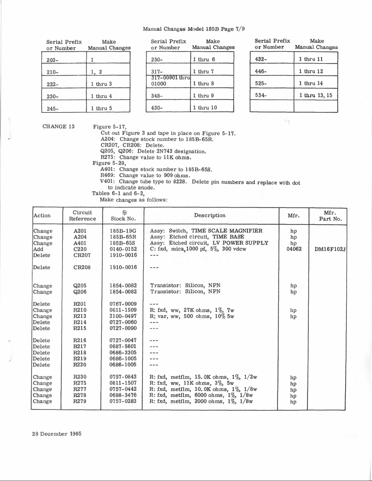
Manual Changes Model 185B Page 7/9
Circuit
1
1,
2
1
thru 3
1
thru 4
1
thru 5
Cut out Figure
A204: Change stock number to 185B65R.
CR207, CR208: Delete.
Q205, Q206: Delete 2N743 designation.
R275: Change value to 11K ohms.
Figure 5-29,
A401: Change stock number to 185B-65s.
R469: Change value to 909 ohms.
V401:
Tables 6-1 and 6-2,
Make changes
203210222230245-
CHANGE 13 Figure 5-17,
Action
Reference
Serial
or Number
430-
3
and tape in place on Figure 5-17.
Change tube type to 8228. Delete pin numbers and replace with dot
to
indicate anode.
as
follows:
Prefix
2
50-
317317-00901 thru
01000
348-
@
Stock No.
Make
Manual Changes
I
1
thru 6
I
1
thru
7
1
thru 8
1
thru 9
1
thru
10
Description
1
a
Serial
or
I
432-
I
446-
Prefix
Number Manual Changes
I
I
I
Mfr.
Make
1
thru
1
thru 12
1
thru 14
1
th~
11
13.15
Mfr
Part
.
No.
Change
Change
Change
Add
Delete
Delete
Change
Change
Delete
Change
Change
Delete
Delete
Delete
Delete
Delete
Delete
Delete
Change
Change
Change
Change
Change
A201
A204
A401
c220
CR207
CR208
Q205
Q206
R201
R210
R213
R214
R215
R216
R217
R218
R219
R220
R230
R275
R277
R278
R279
185B- 19G
18
5B- 6 5R
18 5
B- 6 5s
0140-01 52
1910- 001 6
1910- 0016
1854- 0082
1854- 0082
0767- 0009
0811-1509
2
100- 0497
0727-0060
0727-0090
0727-0047
0687- 5601
0686-3305
0686- 1005
0686-1005
0757-0843
0811- 1507
0757-0442
0698-3476
0757-0283
Assy: Switch, TIME SCALE MAGNIFIER
Assy: Etched circuit, TIME BASE
Assy: Etched circuit,
C: fxd, mica,lOOO pf, 5%, 300 vdcw
LV
POWER SUPPLY
---
---
Transistor: Silicon, NPN
Transistor: Silicon, NPN
---
R
fxd,
ww,
R; var,
27Kohms,
ww,
500 ohms, 10% 5w
176,
7w
---
---
R: fxd, mefflm, 15.OK ohms,
R: fxd,
R: fxd, mefflm, 10. OK ohms,
R: fxd, mefflm, 6000 ohms,
R: fxd, mefflm,
ww,
11K ohms, 3%, 5w
2000
ohms,
l%,
1%
176,
1%,
1/2w
1/8w
1/8w
1/8w
DM16F102;
28 December 1965
Page 10
1
thru
1
thru 4
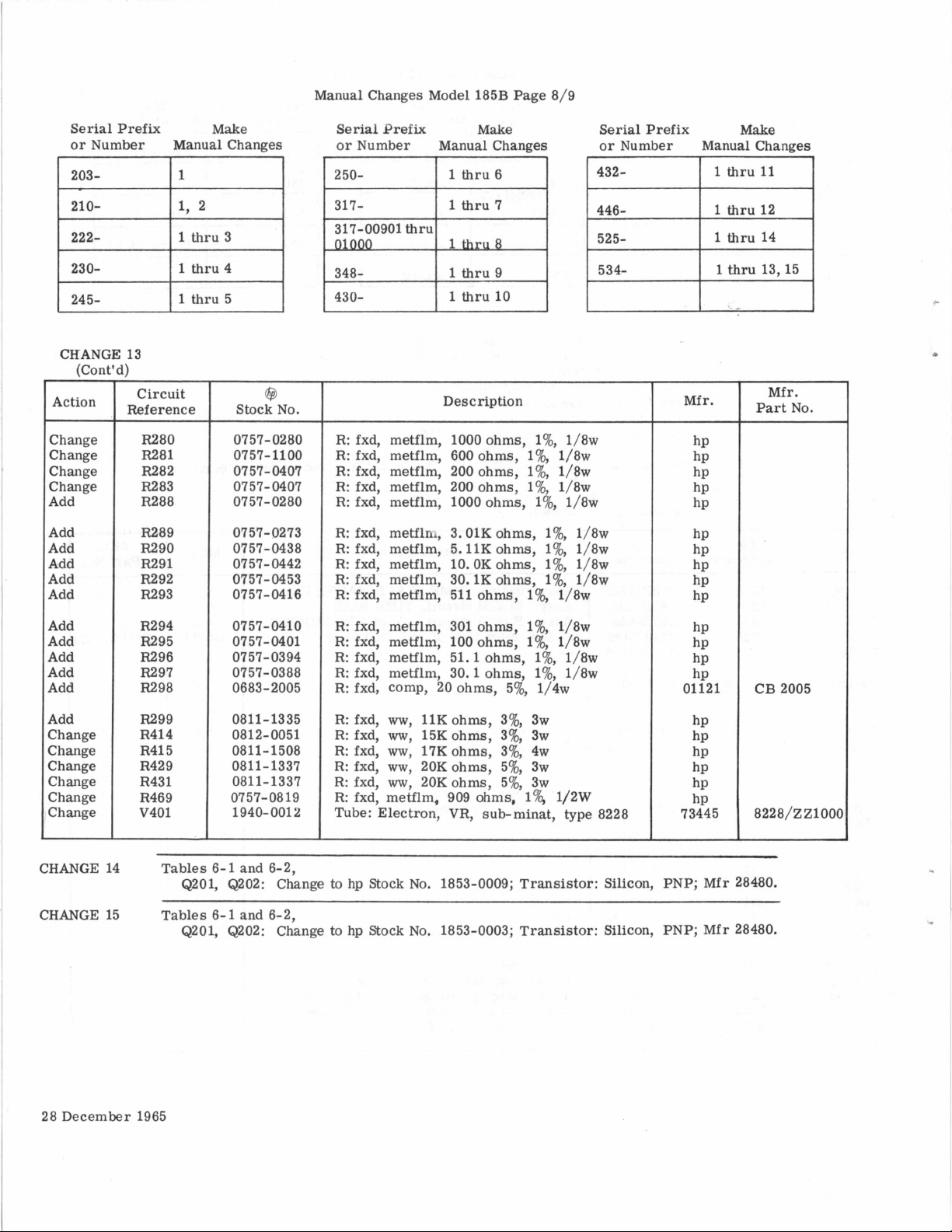
Manual Changes Model 185B Page 8/9
Serial
Prefix
or Number Manual Changes
3
317-00901 thru
01000
348430-
Make
1
thru8
1
thru
1
thru 10
Serial Prefix Make
or Number Manual Changes
1
thru
11
1
thru 12
1
thru 14
1
thru
9
13,15
1
CHANGE 13
(Cont'd)
~~
Action
Change
Change
Change
Change
Add
Add
Add
Add
Add
Add
Add
Add
Add
Add
Add
Add
Change
Change
Change
Change
Change
Change
Circuit
Reference
R280
R281
R282
R283
R288
R289
R290
R291
R292
R293
R294
R295
R296
R297
R298
R299
R414
R415
R429
R431
R469
V401
@
Stock No.
0757-0280
0757-1100
0757-0407
0757-0407
0757-0280
0757- 0273
0757- 0438
0757- 0442
0'757-0453
0757-0416
0757-0410
0757-0401
0757- 03 94
0757-0388
0683-2005
081
1
-
13
35
0812-0051
0811- 1508
0811-1337
0811-1337
07
57- 08 19
1940-0012
Description
R: fxd, metflm, 1000 ohms,
R: fxd, metflm, 600 ohms,
R: fxd, metflm,
R: fxd, metflm,
R: fxd, metflm, 1000 ohms,
R: fxd, meffln,,
R: fxd, mefflm, 5.11K ohms,
R: fxd, metflm,
R: fxd, mefflm,
R: fxd, metflm, 511 ohms,
R:fxd, metflm, 301 ohms,
R: fxd, mefflm, 100 ohms,
R: fxd, mefflm, 51.1 ohms,
R: fxd, metflm, 30.1 ohms,
R: fxd, comp, ZOohms, 5%, 1/4w
R: fxd,
R: fxd,
R: fxd,
R: fxd,
R: fxd,
R: fxd, mefflm, 909 ohms,
Tube: Electron, VR, sub-minat, type 8228
ww,
ww,
ww,
ww,
ww,
200
ohms,
200
ohms,
3.01K ohms,
10. OK ohms,
30.1K ohms,
11K ohms, 3%, 3w
15K ohms, 3%, 3w
17Kohms,
20K ohms, 5%, 3w
ZOKohrns, 5%, 3w
1%,
1%,
1%,
I%,
I%,
l%,
1%,
17%
1%,
1%,
3%, 4w
17%
1/8w
1/8w
1/8w
1%,
1%,
1%,
I%,
1/8w
1/8w
1/8w
1/2W
1/8w
1/8w
1/8w
1/8w
1/8w
1/8w
1/8w
1/8w
Mfr.
Mfr.
Part No.
CB
2005
8228/ZZlOOO
.
CHANGE 14
CHANGE 15
28 December 1965
I
i
~
Tables 6-1 and 6-2,
Q201,
Q202:
Tables 6-1 and 6-2,
Q201, Q202: Change to hp Stock No. 1853-0003; Transistor: Silicon, PNP; Mfr 28480.
Change to hp Stock No. 1853-0009; Transistor: Silicon, PNP; Mfr 28480.
Page 11

Serial Prefix Make
or Number Manual Changes
222-
1
thru
3
25031
-1
01
7-
000
thri.
1
1
1
thru
thru
thru
6
7
8
Serial Prefix Make
or Number Manual Changes
1
thru
11
1
thru
12
1
thru
14
230245-
CHANGE
(Cont’d)
13
I
1
1
thru
thru
4
5
348- 1
430- 1
CUT 4LONG DOTTED LINE
1-
- - - - - - - - -
CUT 4LONG DOTTED LINE
thru
thru
- -
9
10
I
534-
1
1
thru
13 , 15
1
28
December
1965
Figure
3
I
I
I
I
I
I
I
-1
I
Page 12
OPERATING AND
SERVICE
MANUAL
MODEL
SERIALS
PREFIXED:.
1856
144-
OSCILLOSCOPE
Copirieht
1501
?AOE
WEWlE??-?ACKAID COHPANY
MI11
ROAD.
PA10 AllO. CALIFORNIA,
1961
U.S.A.
Page 13

Table of Contents
Model
185B
TAB18
Section Page
I GENERAL INFORMATION
1.1
.
Introduction
1.3
.
Options
1.6
.
Instrument Identification
1.8
.
Description
1.14
.
Cathode-Ray Tube Warranty
II
PREPARATION FOR USE
.
Incoming Inspection
2.1
2.2
.
2.4
.
2.6
.
2.8
.
2.10
.
2.12
.
Installation
.
2.13
.
2.16
2.18
.
2.20
.
Associated Equipment Available
2.22
.
Reshipment
III
OPERATINGINSTRUCTIONS
Introduction
3.1
.
Front Panel Controlsand Connectors
3.4
.
Rear PanelConnectors
3.6
.
The Principle of the Sampling
3.8
.
Triggering the Model
3.13
.
3.14
.
General
3.17
3.27
3.30
3.31
3.35
3.37
IV
PRINCIPLESOFOPERATION
4-
4.4
4.5
4.7
4.9
4.13
4.17
4.19
4.21
4.23
4.26
4.31
4.32
4.34
4.36
Triggering Methods
.
Effects of FM and Jitter
.
.
Pulse
.
Observation of Intermittent Pulses
.
Examining Pulse Irregularities
.
Operating Instructions
1
.
Introduction
.
BlockDiagram Description
.
General
.
Input Circuits
.
Ramp-GateGenerator
.
Time-Base Circuits
.
Calibrator
.
Vertical Amplifier
.
Horizontal Amplifier
.
Time.BaseDetermination
.
TunnelDiode Operation
.
Triggering Circuits
.
General
.
Trigger Input
.
Ramp-Gate Generator Circuits
.............
MechanicalInspection
Power Requirements
230-Volt Operation
Three-Conductor Power Cable
Operational Check
Cooling
Cabinet Mount
Rack Mount
Oscilloscope
Electronic Switch
............
............
Analysis
............
............
........
...........
.....
...........
....
........
........
.....
......
.......
.......
...........
.........
..........
...........
...........
..........
..........
...........
.........
...........
.........
......
......
185B
....
......
......
......
......
....
.....
......
arid
.......
......
.....
......
.......
.
.
. .
.
.
.
OF
1-1
1-1
1-1
1-1
1-1
1-3
2-1
2-1
2-1
2-1
2-1
2-1
2-1
2-1
2-1
2-1
2-1
2-2
2-2
3-1
3-1
3-1
3-3
3 -4
3-4
3-4
3-5
3-6
3-6
3-6
3-6
3-6
4-1
4-1
4-1
4-1
4-1
4-1
4-1
4-2
4 -2
4-2
4-2
4-2
4-3
4-3
4-3
4-4
CONTENTS
Section Page
IV PRINCIPLES OF OPERATION (Cont'd)
4.46
.
Ramp-Gate Extender
Voltage Generator Circuits
4.54
.
Time-Base Circuits
4.56
.
Comparator
.
4.66
4.71
4.77
4.81
4.87
4.95
4.96
4.101
4-103.High-Voltage
4.106
V
MAINTENANCE
5.1
5.3
5.5
5.6
5.8
5.10
5- 12
5.15
5.17
5 . 30
5.31
5.34
5.37
5.41
5.43
5.45
5.47
5.51
5.53
5.57
5.59
5.67
5.68
5.69
5.70
5.72
5.73
5.75
VI
REPLACEABLE PARTS
6.1
6.4
Time Scale/Time Scale
Relationship
.
Delay Circuits
.
Comparator Blocking Oscillator
.
Horizontal-Scancircuits
.
Calibrator
.
Vertical Amplifier
.
General Operation
.
Transients
.
Low-Voltage Power Supplies
.
Introduction
.
Test InstrumentsRequired
.
Periodic
.
Cleaning
.
General Maintenance
.
Cabinet Removal
.
Troubleshooting
.
System Troubleshooting
.
SectionalTroubleshooting
.
Repair
Access
.
and Fan Motor
.
Replacement of Semiconductors
.
Servicing Etched Circuit Boards
.
CRT Replacement
Adjustment Following Repair
.
.
Adjustments
Low-Voltage
.
.
High-Voltage
.
Vertical Amplifier
.
Sync Circuit
.
Time Base
.
Performance Check
.
Time Calibrator
.
Sync Pulse
.
Amplitude Calibrator
.
Time Scale
.
Minimum Delay
.
Trigger Sensitivity
.
Introduction
.
Ordering Information
..........
.............
..........
Plower
............
...........
Maintenance
the
Air
.............
to Power Transistors
..........
Power
Power
..........
...........
...........
..........
...........
and
Ramp-
.......
.........
Magnifier
.........
.....
........
.......
Supply
....
...
....
.......
Filter
.....
......
........
.........
....
....
........
......
...
'Supplies
Supply
...
...
.......
.......
........
......
........
.......
.........
.......
.
.
.
.
.
4-6
4-7
4-7
4-8
4-9
4-9
4-10
4-12
4-12
4-12
4-13
4-13
4-13
5-1
5-1
5-1
5-1
5-1
5-1
5-1
5-1
5-1
5-1
5-4
5-4
5-4
5-5
5-5
5-6
5-6
5-6
5-7
5-7
5-7
5-7
5.16
5-10
5-10
5-10
5-10
5-10
5-10
6-1
6-1
6-1
~
ii
01255-1
Page 14
Model
185B
LIST
Of
ILLUSTRATIONS
List
of
List of Tables
Illustrations
Number Title Page
1.1
.
1.2
2.1
2.2
3.1
3.2
3.3
3.4
3.5
3.6
3.7
3.8
3.9
3.10
3.11
3.12
3.13
3.14
4.1
4.2
4.3
4.4
4.5
4.6
4.7
4.8
4.9
4.10
4.11
4.12
Model
.
Cathode-Ray Tube Warranty
.
Associated
.
Dimensions for
.
Operating Controls and Connectors
.
Rear Panel Controls
.
Viewing Signals Above
.
Viewing Signals Below
.
Viewing Signals Below
.
Viewing Signals Below
.
Free Running Trace
.
Unmagnified Trace
.
Magnified Trace
.
Viewing Delayed Signal
.
Using Delayed Trigger
.
Delayed Sync Pulse
.
External Scan
.
Recording the Signal
.
Overall BlockDiagram
.
Time-Base Determination
.
Tunnel-Diode Operation
.
Triggering-Circuit Block Diagram
.
Tunnel-Diode Count-Down Circuit
Ramp Generator
.
.
Time-Base BlockDiagram
.
Ramp Voltage vs Time
.
Effects of Delay
.
Staircase Generator
.
Vertical Amplifier Block Diagram
.
High-Voltage Power Supply
185B
Oscilloscope
Dual-Trace Vertical Plug-In
($9
Equipment Available
Rear
with
Support
.........
10
kc
10
kc by Using
Delayed Trigger
SYWC
PULSE OUT
Circuit under Test
Block Diagram
...........
10
kc by Using
..........
10
kc when the
..........
.........
..........
...........
........
........
..........
............
.........
.....
....
....
........
.....
........
......
.......
Model
187B
Unit
.
.
1-0
......
...
.....
...
......
...
...
...
...
...
...
...
...
...
...
...
...
...
1-3
2-0
2-3
3-0
3-2
3-5
3-5
3-5
3-5
3-7
3-8
3-9
3-10
3-11
3-12
3-13
3-13
4-0
4-2
4-3
4-4
4-5
4-6
4-8
4-a
4-10
4-11
4-13
4-13
Number Title Page
5.1
.
Driving the Trigger Circuit
.
Trigger Circuit Waveforms
5.2
Disassembly for Power Transistor
.
5.3
Replacement
.
MinimumDelay Measurement
5.4
5.5
.
Calibrator Instrument Setup
.
Top View, Model
5.6
5.7
.
Left Side
5.8
.
Right Side View, Model
5.9
.
Bottom View, Model
.
5.10
5 .ll
5.13
5.14
5.15
5.16
5.17
5.18
5.19
5.20
5.21
5.22 . A602
5.23
5.24
5-25
5.26
5.27
5.28
5.29
5 .30
5.31
5.32 . A302
5.33
A103
.
Waveforms
5.12
.
Parts Location, Switch Assemblies
.
Trigger Circuit, Schematic Diagram
.
A204
.
Waveforms
.
Parts Location, Switch Assemblies
.
Time-Base Circuit, Schematic Diagram
.
A1
.
Waveforms
.
Assembly Location
.
Main Vertical Amplifier,
Schematic Diagram
.
Waveforms
.
Assembly Location
.
Parts Location, Calibrator and Sync Pulse
Switch,
.
Calibrator and Sync Pulse Generator,
Schematic Diagram
.
A401
.
Assembly Location
.
Low-Voltage Power Supply,
Schematic Diagram
.
A301
.
Assembly Location
.
High-Voltage Power Supply,
Schematic Diagram
View,
Component Location
Component Location
and
A2
Component Location
Component Location
S601,
and
A402
Component Location
High-Voltage Rectifier Assembly
............
185B
Model
185B
.............
.............
.............
..........
.............
..........
with Amp1 . Conn
.........
Component Location
..........
.........
..........
......
......
.....
......
........
185B
......
185B
......
.......
.......
...
.
.
.......
...
.....
........
.......
.
5603 . 5-23
.
.
.......
.
........
5-3
5-3
5-5
5-8
5-8
5-11
5-12
5-12
5-13
5-16
5 . 16
5-17
5-17
5-18
5-18
5-18
5-19
5-20
5-20
5-21
5-21
5-22
5-22
5-23
5-23
5-24
5-24
5-25
5-26
5-26
5-26
5-27
LIST
Number Title Page
1.1
.
Specifications
2.1
.
Associated Equipment Available
.
3.1
5.1
5.2
5.3
5.4
01255-1
Methods of Triggering
.
Recommended Test Equipment
.
System Troubleshooting
.
Resistance to Ground
.
Adjustments Following Tube, Transistor,
and
Diode Replacement
............
....
........
.....
........
.........
.......
1-1
2-2
3-4
5-0
5-2
5-4
5-6
Of
TABLES
Number Title Page
5.5
.
Time Scale Adjustments
5.6
.
Condensed Test and Adjustment
Procedure
5.7
.
Amplitude Calibrator Accuracy
.
Time Scale Calibration Check
5.8
6.1
.
Reference DesignationIndex
.
Replaceable Parts
6.2
.............
.......
....
.....
.....
..........
5-8
5-9
5-10
5-10
6-2
6-24
iii
Page 15
Section
Figure
I
1-1
Model
185B
Y
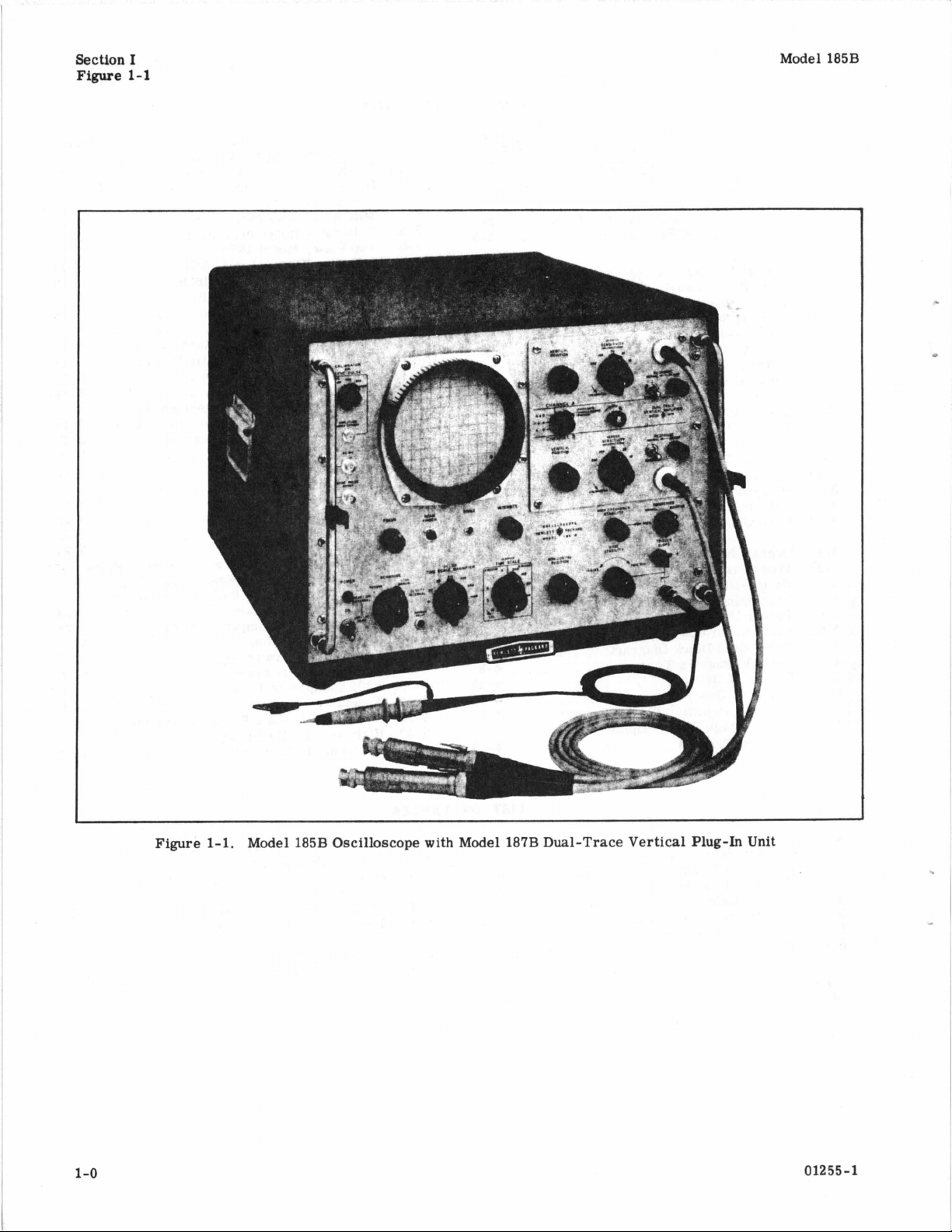
Figure 1-1. Model 185B Oscilloscope with Model 187B Dual-Trace Vertical Plug-In Unit
1-0
~
01255-1
Page 16

Model
185B
Paragraphs
Section I
1-1
to
1-10
SECTION
GENERAL INFORMATION
1-1.
INTRODUCTION.
1-2.
This manual gives operation and maintenance
information for the
An operational check
operation
performance check
specifications during incoming inspection
paragraph
1-3.
1-4.
P2
phosphor with external graticule.
options, however, are available:
a.
b. Option
c. Option
d:
e.
1-5.
option
differences in crt persistence, color, and oscilloscope
photography techniques, instruments with or without
option
are, however,
(see section VI).
in this manual apply to all options unless otherwise indicated.
is
given in paragraph
5-67.
OPTIONS.
The
Model
Option
Option
Option
1.
P1
Internal graticule in cathode ray
3.
7.
P7 phosphor
11.
P11
31.
P31 phosphor
Option
31
1
is
available only with option
3
are operationally interchangeable. There
some differences in component parts
@
Model
to
185B
assure basic instrument
2-10.
that
may be used for verifying
185B
is
normally supplied with
phosphor
phosphor
is
not available with option
All
references to the Model
Oscilloscope.
A
complete
is
given in
The following
tube
3,
3.
Other than
and
185B
I
1-6.
INSTRUMENT IDENTIFICATION.
1-7.
Hewlett-Packard Company uses a two-section
eight-digit serial number (e.g.
first
three digits of the serial number onyour instru-
ment are not
with
this manual which define differences between
your instrument and
sheets are missing, your Hewlett-Packard engineering representative can supply you with the necessary
information.
144-,
change sheets have been supplied
this
a
1-8.
DCSCRl?TlON.
1-9.
GENERAL. The
provides
ena
will
below
spaced.
signal
operate reliably.
above
obtain jitter-free presentation.
1-10.
high speed characteristics
nique. Using this system the entire signal under examination
taken on different occurrences of the input at slightly
later points along the waveform.
a
with repetition rates to
visual display of very high-speed phenom-
present a steady display of pulse repetition rates
100
kc even when the signals are randomly
For frequencies above
is
divided down
100
kc, more uniform spacing
PRESENTATION. The Model
is
scanned, with each succeeding sample
@
Model
so
that the input circuitry will
As
the input frequency increases
by
000-00000).
manual. If
1000
mc. The instrument
100
185B
kc,
is
these
Oscilloscope
the
185B
using the sampling tech-
Each time such a
If the
change
incoming
required
obtains
to
it8
I
HORIZONTAL
Sweep Speeds:
10 ranges,
within
between ranges and increases fastestunmaanified
sweep speedto
sweep
the exception of time represented by
of
the unmagnified sweep.
Magnification:
7
calibrated ranges
and
X100.
speed to
sweep speed
Intensity and sample density are not affected by
magnification.
Delay Control:
Three-turn
when using magnified sweep. Permits any
tion of unmagnified trace
10
nsec/cm
Vernier gives continuous adjustment
&5%.
4
is
maintained at all magnifier settings with
Increases maximum calibrated sweep
0.1
nsec/cm; with vernier, maximum
is
further extended to
variable delay control
to
10
psec/cm, accuracy
nsec/cm. Accuracy of the basic
X1,
X2,
X5,
X10, X20, X50,
0.04
is
to
be
viewed on screen.
01255-1
Table
first
nsec/cm.
available
1/4
por-
1-1.
Specifications
cm
Minimum Delay (input trigger
Less than
faster. On slower sweep
lay increases to
5
psec on the lO-psec/cm range.
Sample
Continuously adjustable from approximately 70
samples per trace
Scanning Functions:
Internal
for normal viewing.
Record
approximately
Manual
knob.
External
approximately
input impedance greater than
120
Density:
-
X
-
X
-
X
-
nsec at
a
maximum of approximately
to
axis
driven
axis driven by internal slow ramp;
60
seconds for one trace.
axis driven by manual scan control
X
axis
driven
12
volts for 10-cm deflection,
to
start
100
nsec/cm sweep and
speeds,
1000
by
by
minimum de-
samples per trace.
internal staircase
external voltage;
25,000
Specifications cont'd
of trace):
ohms.
1-1
Page 17

Section
Table
I
1-1
(cont‘d)
1-1.
Table
“RIGGER FUNCTIONS
Normal-External Trigger
to
Amplitude: 450 mv
volts rms or 100 volts peak will not damage
input circuit.
Width: 5 nsec at minimum amplitude.
Rate:
50 cps to 1 mc
speed setting. Maximum
100 mc on the 200 nsec/cm
Jitter:
Input Impedance: 50 ohms nominal
Sensitive-External Trigger
Amplitude: *15
Width:
Rate: Same as normal
Jitter:
Input Impedance: 50
High Frequency
Input Frequency: 50 to
Sensitivity: 200 mvpeak-to-peak. Operates from
Jitter: 4% of cycle from 50 to 400 mc;
Signal at Input Connector: Less than 15 mvpeak-
Input Impedance: 50 ohms nominal, ac coupled.
SYNC PROBE
The 185B-21A (use with any trigger function) in-
creases input impedance to more than 7500
ac coupled; reduces sensitivity by approximately
4:l at 10 mc and higher and by approximately 20:l
at
low frequencies.
SYNC PULSE OUTPUT
Amplitude: Positive; at least 1.5 v into 50 ohms
Rise Time: Less than 2 nsec
Width: Approximately 5 psec
Recurrence: One pulse per sample
CALIBRATOR
Voltage:
20 mv, 100 mv,
Time:
Approximately 5 psec burst of 50 mc sinewave.
Frequency accuracy
Less than 0.03 nsec or 0.02% of the time
represented
ever
is
approximately 5:l in the “smoothed” response
position.
Reflection from step of
by
greater (fast rise Signals). Reduced
to
rms or 10 volts peak
circuit.
5 nsec at minimum amplitude
Same as normal
of 200 nsec/cm
smaller signals at some increase in jitter. Up
to 5 volts rms or 15 volts peak will not damage
input circuit.
from 400 to 1000 mc
to-peak, approximately 10 mc
Reflection from step of
less than 8%.
i2 volts peak. Up
on
the lO-Fsec/cm sweep
rate
increases
and
faster
the
unmagnified speed, which-
1/2
nsec
is
*200 mv peak. Up to 5 volts
will
not damage input
ohms
nominal, dc coupled
1000
mc forsweepspeeds
and
faster
1/2
nsec rise time
200
mv, and 1000 mv;
dc
less
8%
rangee.
coupled.
than
of Cycle
*2%.
Specifications (cont’d)
X-Y
RECORDER OUTPUT
X-
and
to
5
to
8%.
is
ohms,
&
minals in all positions of the scanning control. In
the
MANUAL and RECORD positions the voltage
can
be
ventional
Horizontal Output: Approximately
of sweep
v/cm).
Vertical Output: Approximately
graticule,
impedance approximately 1,000 ohms.
GENERAL
Cathode Ray
5AQ mono accelerator with P2 phosphor normally supplied. 2900-volt accelerating potential,
External Graticule (standard):
Edge lighted with controlled illumination, 10 cm
by
axes have 2-millimeter subdivisions.
Power: 115 or 230 volts
approximately
Dimensions:
Cabinet Mount: 14-5/8 inches high, 19 inches
wide, 22-1/8 inches deep
Rack Mount: 12-1/4 inches high, 19 inches
wide, 21 inches deep behind panel
Weight:
Cabinet Mount: Net 65 lb
Accessories Furnished: 185B-21A Sync Probe
Accessories Available:
185A-39A Plug-In Extender
185A-21C Resistive Divider Probe, 5:l division,
185A-21D Resistive Divider Probe,
185A-21E Resistive Divider Probe, 50:l divi-
185A-21F Resistive Divider Probe,
AC-16W 3-ft RG-55 cable for 185A-21C,D,E,F
Associated Instruments:
187B Dual Trace Vertical Amplifier
187B accessories available:
187A-76A BNC Adapter
187A-76B Type
187B-76C 10:
187A-76D Blocking Capacitor
187B-76E 50-ohm T Connector
Model
Model 908A 50-ohm Coaxial Termination
187B-76F Adapters
187B-76G Probe Socket
Model 213A Pulse Generator,
Model 185B
Y-axis
used to make pen recordings with a con-
signals are available at rear
X-Y
recorder.
to
+13 volts at end of sweep (1.2
Source
impedance approx. 20,000 ohms.
-1
volt at bottom (0.2 v/cm), Source
0
volt
+1
volt at top of
at
ter-
start
Tube:
P1,
P7, and
10 cm, marked in centimeter squares. Major
300
250 ohms
sion, 500 ohms
sion, 2500 ohms
sion, 5000 ohms
llOOA
nsec
rise
time k350 mv amplitude
P11
watts
N
Adapter
1
Divider
Delay Line
phosphors available.
*IO%,
50 to
less
60
1O:l
divi-
1OO:l
divi-
than 0.5
cp8,
A.
1-2
01255-1
Page 18

Model
185B
Paragraphs
Section I
1-11
to
1-15
sample
is
taken, the
“spot"
on the
crtis
moved hori-
zontally along the waveform. Thus, a complete pic-
ture of
a
repetitive high speed signal
is
synthesized
by a buildup of image-retaining “dots” on the oscilloscope face
1-11.
The Model
ranging from
nanoseconds per centimeter depending on the
of the TIME SCALE switch. Any part
time scale can
by adjusting the TIME SCALE MAGNIFIER
as
a graph
185B
10
microseconds per centimeter
be
expanded without loss
is
provides
plotted point by point,
10
basic
time
scales
setting
of
this
of
calibration,
switch.
to
10
basic
Built-in time and amplitude calibrators provide a
convenient means
vertical calibration. Intensity of
pendent of duty cycle, and vertical deflection may
adjusted up
185B
to
provides output signals for
of
checking
10
centimeters. In addition, the Model
both
horizontal and
the
trace
X-Y
recorders and
is
inde-
be
provides means for controlling the display either manually or externally.
1-12.
VERTICAL AMPLIFIER. The vertical system
of the Model
such as the Model
185B
includes aplug-in vertical amplifier
187B.
It
is
this amplifier which
determines vertical characteristics such as bandpass,
sensitivity, etc. The vertical plug-in unit
of
the
basic
1-13.
F’igure
185B-21A
Model
Sync Probe shown in
185B
Oscilloscope.
1-1
illustrates the Model
the
figure
with the oscilloscope. The Model
Vertical Amplifier
plug-in unit
Table
1-1
1-14.
CATWODLRAY
1-15.
The cathode-ray tube supplied with the Model
185B
is
is
lists
guaranteed against electrical failure for one
year from the date
Company. The cathode-ray
trated in figure
in the appendix of
is
shown installed, although the
not part of the basic oscilloscope.
the specifications for the Model
TUBE
WARRANTY.
of
sale
by
the
tube
warranty
1-2.
A
sheet
for your use
this
manual.
is
not part
187B
185B.
is
Dual Trace
The
supplied
185B.
Hewlett-Packard
is
illus-
is
included
IEWLETT-PACKARD
01255-1
CO.
PAOC
MILL
ROAD.
PAL0
Figure
ALTO. CALIF.
1-2.
U.S.A.
Cathode-Ray
Tube
Warranty
1-3
Page 19

se~tian
Figure
n
2-1
Model
185B
MODEL
DUAL TRACE
I
CAL AMPL I F I ER
VERT
1878
MODEL 196A/B
OSCILLOSCOPE
CAMERA
MODEL IlOOA
DELAY LINE
MODEL
DELAY
2-0
I
I
I
00A-76
LINE LOAD
A
Figure
2-1.
CONNECTING
Aellociated
@
Equipment
Available
MODEL l85A-76A
SYNC TAKE-OFF
UP
-Y-93
01255-1
Page 20

Model 185B
Section
Paragraphs 2-1
to
II
2-19
SECTION
PREPARATION
2-1.
INCOMING INSPLCTION.
2-2. MECHANICAL INSPECTION.
2-3. Upon receipt of your Model 185B, check the
contents against the packing
strument for any obvious damage received in transit.
If
damage
(Refer
ditional information.)
all re-usable packing material until an operational
check
2-4. POWER REQUIREMENTS.
2-5. The Model 185B requires
115 or 230 volts
which can deliver approximately
2-6. 230-VOLT OPERATION.
2-7.
operated switch
ment. The existing fuse should
2-ampere slow-blow fuse.
Be
erly for the line voltage
power supplies may
switch
2-8. THREE-CONDUCTOR POWER CABLE,
2-9. To protect operating personnel, the National
Electrical Manufacturers' Association (NEMA)
ommends
grounded. This instrument
conductor power cable which, when plugged into an
appropriate receptacle, grounds the instrument. The
offset pin on the power cable three-prong connector
is
the ground pin. To preserve the protection feature
when operating the instrument from
outlet, use
connect the green pigtail to ground.
2-10. OPERATIONAL CHECK.
2-11. The following procedure
for checking basic operation
controls mentioned in the following procedure
shown in figure 3-1. A complete check-out procedure
to
verify specifications
a.
Install the vertical plug-in unit.
gain
to
b.
Turn INTENSITY
c.
Set
100 NSEC/CM,
is
evident, file claim with the carrier.
to
the
warranty sheet in
To
has
been successfully completed.
*lo%,
If
.230-volt operation
is
provided on the rear of the instru-
CAUTION
sure
to
set
the 115-230 volt switch prop-
is
set
to the wrong position.
that
the instrument panel and cabinet
a
three-prong to two-prong adapter and
approximately 50 mv/cm.
full
SCANNING to INTERNAL, TIME SCALE to
DENSITY full clockwise, MODE
list
and inspect the in-
this
facilitate reshipment, keep
single phase,
is
desired, a screwdriver-
be
is
equipped with a three-
of
is
given in paragraph 5-67.
counterclockwise.
manual for ad-
a
power
300
be
to
be
damaged
is
given
the Model 185B. All
source
50
to
watts.
replaced with
used. The
a
60 cps,
if
this
two-contact
as
a
means
Set
vertical
of
rec-
be
are
to
II
FOR
FREE RUN, TIME SCALE MAGNIFIER and CALIBRATOR AND SYNC PULSE OUTPUT switches full
counterclockwise.
d. Center HORIZONTAL POSITION and VERTICAL
POSITION controls.
e.
minutes
vertical plug-in input
f.
pears.
and readjust HORIZONTAL POSITION and VERTICAL
POSITION controls as necessary.
g.
h
mately five cycles of
2-12.
a
2-13. COOLING.
2-14. The Model 185B uses
tem
within the cabinet. The air intake and filter
cated on
ment, choose
of clearance around rear and sides of cabinet..
2-15.
the
be
coated with a
No.
filter
cooling. Refer to paragraph
procedures.
2-16. CABINET MOUNT.
2-17. The Model 185B cabinet mount
instrument.
ated with
plane.
ment to a better viewing angle. Be sure to maintain
clearance required for proper cooling mentioned in
paragraph 2-14.
2-18. RACK MOUNT.
2-19. The standard rack model
rear-support pins and bushings. The bushings
installed on rear flanges. The pins are for use in
mounting the instrument
tended to mate with bushings when instrument
stalled. Do not mount the instrument with only frontpanel screws, particularly
to
any
support pins
securing front panel to rack are not supplied. Install
instrument
USE
Turn the Model 185B on and allow about
for
the instrument
to
Rotate INTENSITY clockwise until a
If
the crt remains
Adjust FOCUS for a
resultant presentation should
The
a
INSTALLATION.
to
maintain tolerable operating temperatures
rear
of instrument. When mounting instru-
a
site
that provides
AIR
air
FILTER. Before operating the Model 185B,
filter,
3
from Research Products Co. In addition, the
should
A
vibration or shock.
located at rear of instrument, should
filter
be
cleaned periodically to insure proper
The instrument
its
front panel in a verticalor near-vertical
bail
is
provided for raising front of instru-
are
shown in figure 2-2. Screws for
as
follows:
to
the 50-mc connector.
50-mc sine wave.
adhesive such
stabilize. Connect the
blank,
press BEAM FINDER
thin,
well-defined
a
forced-air cooling
at
least three inches
as
5-6
for proper cleaning
be
is
is
intended
is
at
installation and are in-
if
installation
Location dimensions for
to
supplied with
trace
approxi-
Filter
a
portable
be
is
two
ap-
trace.
sys-
are
lo-
Coat
oper-
two
are
is
in-
subject
01255-1
2-
1
Page 21

Section
Paragraphs
II
2-20
to
Model 185B
2-23
(9-1
196A/B
Oscilloscope Camera
187B
Dual
Trace Amplifier
1
lOOA
Delay
Line
Sync Take-Off
11OOA-76A
Delay Line
Resistive Dividers
185A-21C
185A-21D
185A-21E
185A-21F
AC-16W
Cable
Load
Use
A
High quality camera for use in
permanently recording oscilloscope
presentations
~~ ~~
A dual-channel vertical amplifier
(plug-in) for Model 185B (shown
installed in figure
Overcomes inherent oscilloscope delay,
allowing
rate
Inserted
line
sumdied
~~
Termination for
(normally suppliedwith Model
system)
~
These dividers provide a means for
obtaining
capacitance input
Delay
(All
cable terminated in 50 ohms)
Connecting
Dividers
rise
pulses
to
to
between
permit sync
with
a
high-impedance, low-
Line
or other 50-Ohm systems.
dividers must
cable
1-1)
times of slow repetition
be
viewed
signal
Model
llOOA
for 185A-21C/F
line
take-off
llOOA
Delay Line
to
Model llOOA
be
used with
and delay
(normally
system)
llOOA
Features
Image
to
object ratio:
(1:
1
available)
Model 196B allows oscilloscope
photograph on either internal
external
I
Sensitivity 4 mv/cm
Badwidth:
1000 mc
Input
2 pf nominal
Rise Time: 0.25
Delay:
Insertion
6
db for both
Termination Resistance: 50
graticule oscilloscopes
DC
to
Impedance:
120
ne
Loss:
channels
l:O.
9
to
200 mv/cm
800mc ueable
lOOK shunted
M
ohma
or
1
to
by
c
3
Division
Input Res.
250 5:
a
500
2500 50:
5000
Ratio
10:
100:
Max
Inpl
VRMS
1
1
1
1
10
15
35
50
J
186A
Switching Time Tester
I
a.
Fabricate a bracket for rear support pins and
fasten pins
b.
c.
port
2-20.
2-21.
is
available from Hewlett-Packard Company
crease the usefulness of your Model 185B. Additional
equipment
in unit. Refer to the manual for operating information
regarding your particular plug-in or contact your
nearest
this
information.
2-2
in
place.
Install
Lift instrument into place, engaging rear-sup-
pins, and secure front panel firmly to rack.
bracket at
ASSOCIATED EQUIPMENT
Figure
2-1 and
is
available for use with the vertical plug-
@
representative and he
rear
table
Measures switching time of transistors,
diodes and tunnel diodes. Teste pulse
response of active and passive net-
works. Triggers Model 185B in
vance of pulse output. Accessory
universal adapter available.
of rack.
AVAILABLE.
2-1 show equipment
will
supply you with
to
that
in-
to
Pulse output: 0.1
Pulse Rise Time:
Pulse Repetition
ad-
2-22.
2-23.
dent, repack the instrument using the following procedure
shipping container, taking
in their original positions. (If
was discarded, more may
Hewle
able,
RESHIPMENT.
If,
after
as
a
a.
If
possible, repack the Model 185B in
tt-
Packard Engine e r ing Representative.)
b.
If
the original packaging material
proceed as follows:
(1) Wrap instrument in heavy paper or plastic.
(2)
Use
around
panel
continuously variable
Collector Supply:
Base
Supply:
I
incoming inspection, damage
guide.
care
be
plenty of packing
all
sides of instrument and protect
with
cardboard strips.
material
20 volts peak
LRss
than 1 nsec
Rate:
5 kc
to
50 kc,
0
to
*SO volts
0
to
+lo
volts
is
its
(at
is
least
original
all
material
not avail-
01255-1
to
replace
the
packing
obtained from your
evi-
pads
4
in.)
I
Page 22
Model
185B
(3)
Place
cardboard
or metal
(4)
Mark the
Instrument”,
instrument thus protected
or wooden
bands
to
packing
seal
box
box,
container.
with
‘‘
Fragile”,
and use heavy tape
etc.
Note
If
instrument
Packard Company for service or repair,
attach
type of service or repair
correspondence,
model number
serial number.
a
is
to
be
shipped
tag
identifying owner and indicating
refer
and
to instrument by
complete eight-digit
to
desired.
in a heavy
“Delicate
Hewlett-
In
any
REAR
OF
INSTRUMENT
Figure
Paragraph
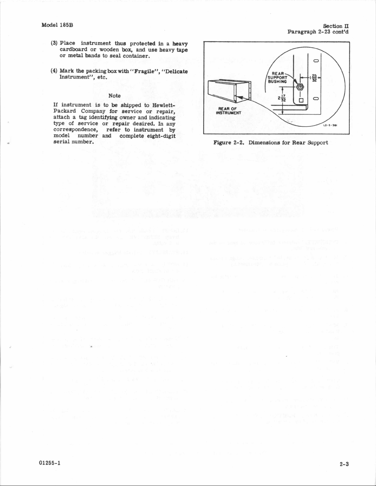
Dimensions for Rear Support
2-2.
Section
2-23
II
Cmt’d
01255-1
2-3
Page 23

Section
Figure
111
3-1
Model 185B
1.
Power switch. Energizes instrument.
2. INTENSITY. Adjusts brilliance of spot on the
cathode-ray
3.
SCALE. Adjusts
with graticule on option 3 instruments.)
4.
FOCUS. Adjusts focus of spot on the cathoderay
tube.
5. BEAM FINDER. Helps locate a presentation
that
is
6.
SCANNING. Adjusts mode of horizontal deflection.
7. SCAN (MANUAL) or DENSITY (INTERNAL).
Used
to
density.
8. TIME SCALE. Adjusts basic time scale of
presentation.
9.
VERNIER. Provides continuously variable time
scale between TIME SCALE ranges.
10.
TIME SCALE MAGNIFIER. Expands
time
scale
11.
DELAY. Enables operator
magnified presentation.
12. HORIZONTAL POSITION. Adjusts horizontal
positioning of presentation.
tube.
scale
brilliance. (Aligns trace
deflected
manually scan display or
off
selected
the
crt.
by
TIME SCALE control.
to
to
adjust scan
the
basic
view any part of
13.
INPUT. Connection for trigger input. Sensitivity: SENSITIVE i200 mv; NORMAL i200 mv
to 2 volts.
14.
STABILITY. Adjusts trigger stability.
15. MODE. Adjusts trigger sensitivity. May
set
to
FREE RUN.
16. TRIGGER SLOPE. Selects desired trigger slope
polarity.
17.TRIGGERING. Set
frequency and amplitude
18. HIGH FREQUENCY STABILITY.
ger stability on HIGH FREQ. position of TRIGGERING.
19.Model 187B
plug-in unit. Not part of
20.SYNC. PULSE OUTPUT. Provides
sync pulse out for triggering
to use as a
21.50 MC. Provides a pulsed 50-mc output.
22. AMPLITUDE DC (OPEN CLRCUIT). Provides
output of four calibrated dc voltages.
23,CALIBRATOR AND SYNC PULSE. Selects
calibrated
to appropriate connectors.
Dual
test
dc
this
switch according
of
trigger signal.
Adjusts
Channel Vertical Amplifier
basic
oscilloscope.
a
test
circuits, or
pulse.
voltages or sync pulse outputs
be
to
trig-
delayed
~~
Figure
3-0 01255-1
3-1.
Operating Controls and Connectors
Page 24

Model 185B
Paragraphs 3-1
Section
to
111
3-5
SECTION
0
P
ERATI
3-1.
INTRODUCTION.
3-2.
This
tion of all controls in the Model 185B Oscilloscope.
If
more theoretical information
Section
3-3. The vertical amplifier system for the Model
185B includes
for operating the plug-in unit are contained in the in-
struction manual for
3-4.
3-5. Figure 3-1 shows
trols and gives a short description of theiruse. Num-
bers
ure
3-1
dicate operational procedure. More detailed information related to
a. BEAM FINDER. Pressing the BEAM FINDER
reduces gain of horizontal and vertical amplifiers to
a point where a “lost” presentation may
adjusted
HORIZONTAL POSITION and VERTICAL POSITION
controls.
b. SCALE. The SCALE control adjusts intensity
of graticule on those instruments provided withanexternal graticule. On internal graticule instruments,
SCALE aligns trace with graticule.
c. INPUT. This connector
chronizing circuits. These circuits insure an exact
time relationship between input signal and moment of
sampling. To operate properly, the sampling oscilloscope
nal that
supply
step
i).
d. TRIGGERING. The TRIGGERING switch may
be
set to SENSITIVE, NORMAL or HIGH FREQ.
pending on amplitude and frequency of trigger signal.
SENSITIVE position
200 millivolts with a frequency below 100 mc. Do not
exceed 10 volts peak input on SENSITIVE position.
NORMAL position
nals (200 mv to
position should be used for trigger signals of
plitudes above 100 mc. The input circuits on HIGH
FREQ. position
1000 mc
circuits.
Do
peak to INPUT when TRIGGERING
SITIVE. Doing
section contains information on the func-
is
desired, refer
IV,
Principles of Operation.
a
plug-in unit. Detailed instructions
that
particular unit.
FRONT PANEL CONTROLS AND
CONNECTORS.
all
front panel operatingcon-
in figure 3-1 are given
to the photograph and do not necessarily in-
these
to
center of cathode-ray tube using the
either
must
be
is
time-related to the input signal, or must
a
sync pulse to trigger circuit under
is
is
2
volts) below 100 mc. HIGH FREQ.
will
so
they may
not connect any voltage exceeding 10 volts
divide down signals
be
CAUTION
so
may damage inputcircuits.
to
relate the
controls
is
accurately triggered by a sig-
used for trigger signals below
used for higher amplitude sig-
used
to
is
listed
be
the input
operate synchronizing
is
on SEN-
N G I
text
in fig-
below:
found and
to
the syn-
test
all
as
high as
to
(see
de-
am-
111
NSTRU
adjusts frequency of count-down oscillator, enabling
it
either positive-going or negative-going slope
signal.
of input circuits
same point on input signal.
full
sync circuits will
at a 100-kc rate.
quency above
near 100
of the input signal.
triggering stability for repetition
by
PUT connector provides
is
With sync pulse from SYNC PULSE OUTPUT connected
in Model 185B
delaying input signal for the purpose of examining
fast
wave output, synchronized with pulse from SYNC
PULSE OUTPUT. Frequency of sine wave
cycles. This signal
reference on the cathode ray tube, or for checking
time
nector provides dc voltages selected by CALIBRATOR
AND SYNC PULSE switch for calibration of vertical
amplifier in oscilloscope. Voltages selected are accurate to within i3$~ of selected value.
when in
sync pulse output and pulsed 50-mc output to appropriate jacks. On other positions of this switch,
voltage
CUIT) connector
mines time
time calibration of
fications when VERNIER control
clockwise.
fine adjustment between any
TIME SCALE switch, resulting in continuous variation
of time scale from
CTI
0
NS
e.
HIGH FREQUENCY STABILITY. This control
to
lock
in
at a submultiple of input trigger frequency.
f.
TRIGGER SLOPE. The TRIGGER SLOPE switch
may
be
used
to
synchronize Model 185B circuits
of
g. MODE. The MODE control adjusts sensitivity
clockwise
kc
h. STABILITY. The STABILITY control adjusts
varying hold-off time in triggering circuits.
i.
SYNC
PULSE OUTPUT. The SYNC PULSE OUT-
delayed 130 nanoseconds from trigger initiation.
to
circuit under
rise
time.
MC. This connector provides
j.
50
scales
k. AMPLITUDE (DC OPEN CIRCUIT). This con-
m. CALIBRATOR AND SYNC PULSE. This switch,
full
is
supplied to AMPLITUDE (DC OPEN CIR-
n. TIME SCALE. The TIME SCALE switch deter-
p. VERNIER. The VERNIER control provides
so
they
will
trigger reliably
If
MODE control
to
FREE RUN position, Model 1858
free
run,
i.e.
sample automatically
If
they
are
triggered withafre-
100
kc,
they
will
but
will
synchronize with a submultiple
test,
is
overcome. The effect
is
valuable for setting up a time
on oscilloscope.
counterclockwise position, connects both
as
explained in step
scale
in nsec or p sec per centimeter. The
this
switch
operate
a
fast
inherent delay (0.1 psec)
is
two
IO
psec/cm to 3 nsec/cm
at
a
frequency
rates
above 100
rise
time pulse
is
similar
a
pulsed sine
is
50 mega-
k.
correct within speci-
is
full Counter-
steps selected
on
trigger
at
the
is
set
kc
that
to
a
dc
by
a
01255-1
3-1
Page 25

Section
Figure
III
3-2
Model
185B
1.
Regulated dc output connector
instruments.
2.
Channel A vertical output voltage
deflection present on
187B). Sensitivity 0.2 volt/cm, Graticule
Center:
3.
Channel B vertical
as
item
0
2.
volt.
For
output.
this
use
for
use with future
for
connector (with Model
with
X-Y
Same
characteristics
vertical
recorder.
-
4. OUTPUT TIME BASE SCAN. Horizontaldrive
voltage
with
Sweep
5. INPUT EXT SCAN. Connect
drive
volts/cm, Input Range:
6.
115-230 Volt Switch.
used.
volt operation, 2-ampere slow-blow fuse
230-volt operation (see section
is
available at
X-Y
recorder. Sensitivity:
Start:
0
volt.
signal
to
this
connector. Sensitivity:
0
Use
4-ampere slow-blow fuse
Set
this
connector.
external
to
12
volts.
to
line voltagebeing
VI).
1.2
volb/cm,
horizontal
for
POWER
CORD
For
use
1.2
115-
for
3-
Figure
2
3-2.
Rear-Panel Controls
01255-1
Page 26

Model
185B
Paragraphs
Section
3-6
to
111
3-7
.
q.
TIME SCALE MAGNIFIER. The TIME SCALE
MAGNIFIER switch
selected by TIME SCALE switch
by TIME SCALE MAGNIFIER switch.
r.
DELAY. The DELAY control selects any part
of unmagnified presentation for magnification;
with delay control you effectively slide cathode-ray
tube along expanded presentation
divides
the value
by
number selected
to
view portion you
that
has
been
i.e.,
want
8.
SCANNING. The SCANNING switch determines
type
of horizontal deflection
point
it
should
beam across the face of the cathode-ray tube
relation
The beam may
of the tube and yet the time
ample,
185B
deflection; they
to
50
provides a choice
(1)
INTERNAL. The time
setting of TIME SCALE and TIME SCALE
MAGNIFIER switches. On INTERNAL, the
beam
of the tube
DENSITY control and sampling frequency.
(2)
MANUAL. On MANUAL position, scanning
accomplished
DENSITY (INTERNAL) control. Manual operation may
sweep
the only visible portion of trace
illuminated by setting of MANUAL SCAN control. The time scale in seconds per centimeter
is
determined again
MAGNIF'IER and TIME SCALE switches. Man-
ual scan
it
is
e.g., when
RECORD. On RECORD position, operation
exactly the same as on MANUAL except
in
very slowly across
time scale determined by setting
SCALE MAGNIFIER and TIME SCALE switches.
RESET OR EXTERNAL. The RESET OR EXTERNAL position
vides a means for resetting scan when oper-
ating on RECORD position,
a
means of scanning with an external signal.
An input connector, INPUT EXTERNAL SCAN,
is
horizontal input,
t.
SCAN (MANUAL) - DENSITY (INTERNAL), The
function of this control depends on setting of SCANNING switch.
NAL, the SCAN (MANUAL)
control adjusts number of samples per centimeter
and hence the density of sample dots
viewer. Reducing scan density
ing up the physical speed of horizontal sweep,
be
emphasized
its
time scale in seconds per centimeter.
take
10
nanoseconds per centimeter. The
are
as
is
automatically swept across the face
at
an actual speed determined
by
be
thought of as a condition where
is
always present on oscilloscope, but
is
useful in
necessary
fast
spikes are present on waveform.
this
case the beam
provided on rear of instrument for external
With
SCANNING switch
that
will
be
used.
At
that
apparent speed of
has
seconds to go across the face
scale
could
be,
for ex-
Model
of
four
follows:
adjusting SCAN -(MANUAL)
to
carefully trace presentation,
has
modes of horizontal
scale
is
determined
is
that
by
setting of TIME SCALE
x-Y
recorder work when
is
automatically swept
the
face of the tube
of
two
functions:
or
-
DENSITY (INTERNAL)
has
the effect of speed-
1)
2)
it
provides
set
to
INTER-
as
seen by the
TIME
it
this
no
by
by
is
part
is
that
at
pro-
i.e.,
-
a
the actual speed
oscilloscope face. However, turning
no effect on time scale in seconds per centimeter on
cathode-ray tube. On the MANUAL position of the
SCANNING switch, the SCAN (MANUAL)
(INTERNAL) control moves dot along presentation
explained in step
EXTERNAL positions of SCANNING, the SCAN
UAL) - DENSITY (INTERNAL) control
3-6.
REAR PANEL CONNECTORS.
3-7.
Figure
and gives a short description of their uses.
figure
the figure to the photograph and do not necessarily
indicate operational procedure. The following paragraphs give more detailed information about
connectors:
nector
sory instruments. The following voltages
able with reference to ground (pin
Channel
terminals for use in driving an
the Model
nector
0
(0.2
20,000
Channel
terminals. Output characteristics of CHAN B are
identical
scan voltage
available at this connector to drive horizontal
of X-Y recorder. The output from OUTPUT TIME
BASE SCAN
and
Source impedance
means of controlling scan with an external signal.
The scan voltages required
supplied by OUTPUT TIME BASE SCAN connectors,
i.e.,
about
HORIZONTAL POSITION centered). Input resistance
varies with setting
minimum
connects Model
voltage setting selected.
fuse
3-1,
a.
5401,
is
intended
1)
Pin b,
2)
Pin c,
3)
Pin d,
4)
Pin
e,
b.
OUTPUT CHAN
A
is
approximately
volt in center, and
volt/cm). Source impedance
ohms.
c.
OUTPUT CHAN
B
to
d. OUTPUT TIME BASE SCAN. The horizontal
+12
volts
e.
INPUT EXT SCAN. This connector provides
0
volt
+13
is
f.
115-230
(see
section VI).
to
produce one complete picture on
this
control
-
has
DENSITY
as
s(2).
On RECORD and RESET
3-2
shows
all
connectors on
the numbers in figure
is
3-2
inoperative.
rear
relate
OR
(MAN-
panel
As
in
text
in
these
regulated dc output connector. This con-
to
supply
dc
power tofuture acces-
are
avail-
a):
+12.6
volts
-12.6
volts
+250
volts
-100
volts
A.
The vertical output from
of the plug-in unit
187B
installed. The output from this con-
+1
-1
B.
of the plug-in unit
those of CHAN
that
has been selected
is
approximately 0 volt at sweep
at
sweep termination
is
approximately
is
available at these
X-Y
recorder with
volt at top of graticule,
volt at bottom of graticule
is
approximately
The vertical output from
is
available
A.
by
at
these
SCANNING
is
axis
start
(1.2
volts/cm).
20,000
ohms.
a
are
the same
to
position scan at left edge of crt, and
volts to position scan at right edge (with
of
time scale VERNIER
32.3K.
volt switch. This switch automatically
185B
power transformer for line
Be
sure
to use correct line
as
but
those
the
01255-1
3-3
Page 27

Section
Paragraphs
III
3-8
to
3-15
Table
3-1.
Methods
of
Triggering
Model 185B
r
r
3
r
Waveform
Types
Trigger Freq
Over 10
Below
Below 10
Below 10
10
kc
kc
kc
kc
Possible
Trigger Ckt
Measurement?
to
under
no
Ext
Trig
Gen
4vailable
no
---
Delay
iequired
‘
(no,
test
delay
120 ns)
Line
no
Yes
no
yes
if
ckt
>
1
Xefer
Figure
3-
3
3-4
3-5
3-6
to
3-8.
THE
PRINCIPLE
OSCILLOSCOPE.
3-9.
The action of the sampling oscilloscope issim-
llar
to a strobe light that
nization with a turning device, resulting in an apparent slow motion--or the effect of taking moving pictures of a rapidly spinning wheel where
shutter speed
rotation of the wheel, causing the wheel to appear
be turning very slowly, or even turning backwards.
3-10. The sampling of the
oscilloscope
same way. The sampler plug-in in this case would
represent the camera shutter and lens. The sampling
circuit
input voltage
occurs over and over again,
sample taken on a succeeding repetition of input sig-
nal
reference point on input signal.
3-11. THE VIEWING ‘WINDOW”. There
maximum and minimum time during which sampling
oscilloscope may complete each observation. In the
Model 185B, maximum time
imum time approximately
is
and at a slightly later time with respect to same
is
nearly
is
accomplished in almost exactly the
opened for very short periods of time and
at
that
time
OF
THE
SAMPLING
is
slightly out of synchro-
the
the
same as the time for one
signal
is
carefully measured. This
is
0.3
with the sampling
with
each succeeding
is
acertain
100 pseconds and min-
nanoseconds. This time
camera
to
is
referred
120 nanoseconds for the “window” to open after trig-
ger
is
100
pseconds will require special triggering tech-
niques when
3-12. In
cuits must be delayed, or
used to permit viewing leading edge of this
signal. The following paragraphs will describe different methods available for solving some synchronization problems you may encounter in sampling oscilloscope technique.
3-13.
3-14. GENERAL.
3-15.
be
synchronized with a signal
signal received by vertical amplifiers. Furthermore,
the system must
because sampled signal never actually enters oscilloscope circuits, and therefore
ternally for synchronization (in the case
187B, signal
figures 3-3
and
measurement situations, and give recommended
instrument arrangement.
to
as
theviewing“window”. Since
received, signals with a period greater than
it
is
necessary to view rise time.
this
case, either
TRIGGERING THE MODEL
As
in any oscilloscope, the
be
is
sampled at probes). Table 3-1 and
to
3-6
list
the
signal
to
an
advanced trigger must
185B.
Model
that
is
time-related to
externally synchronized.
is
not available in-
common types of waveforms
it
sampling
type
185B must
This
of
Model
takes
cir-
be
of
is
3-4
01255-1
Page 28
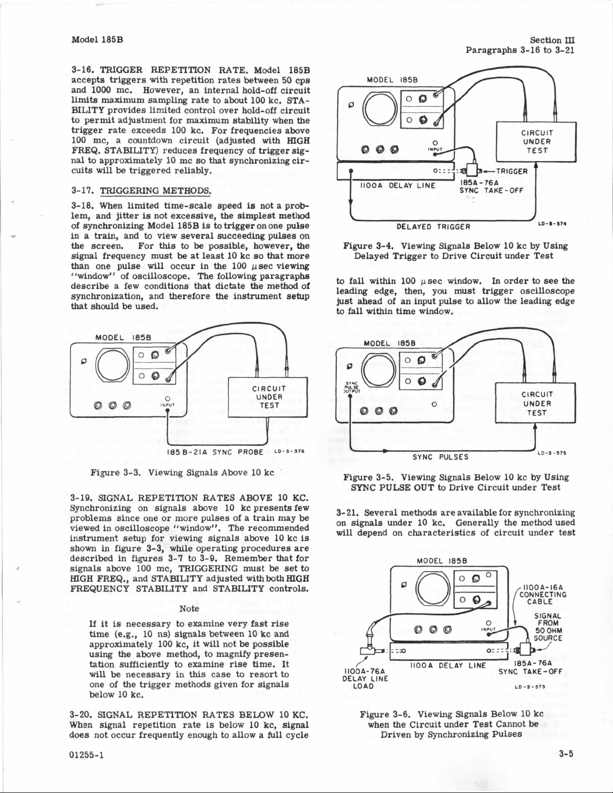
Model 185B
Section
III
Paragraphs 3-16 to 3-21
3-16. TRIGGER REPETITION RATE. Model 185B
accepts triggers
with
repetition
rates
between 50 cps
and 1000 mc. However, an internal hold-off circuit
limits
maximum sampling rate to about 100 kc. STABILITY provides limited control over hold-off circuit
to permit adjustment for maximum stability when
the
trigger rate exceeds 100 kc. For frequencies above
100 mc,
a
countdown circuit (adjusted with HIGH
FREQ. STABILITY) reduces frequency of trigger sig-
nal to approximately 10 mc
cuits
will
be
triggered reliably.
so
that synchronizing cir-
3-17. TRIGGERING METHODS.
is
3-18. When limited time-scale speed
lem, and
of synchronizing Model 185B
in a train, and
the screen. For
signal frequency must
than one pulse
jitter
is
not excessive, the simplest method
is
to
trigger on one pulse
to
view several succeeding pulses on
this
to
be
be
will
occur in the 100 Fsec viewing
possible, however, the
at
least
10
notaprob-
kc
so
that
more
“window” of oscilloscope. The following paragraphs
describe a few conditions that dictate
the
method
of
synchronization, and therefore the instrument setup
that
shculd
MODEL
be used.
1856
MODEL
A
IIOOA DELAY LINE
I1
L
1858
SYNC
185A-76A
DELAYED TRIGGER
TAKE-OFF
CIRCUIT
UNDER
TEST
J
LD-S-
574
Figure 3-4. Viewing Signals Below 10 kc by Using
Delayed Trigger to Drive Circuit under Test
to
fall
within 100 Fsec window.
In
order
to
see
the
leading edge, then, you must trigger oscilloscope
just ahead of an input pulse to allow the leading edge
to
fall within time window.
CIRCUIT
QQQ
185
B12IA SYNC PROBE
UNDER
TEST
L
LO-S-576
Figure 3-3. Viewing Signals Above 10 kc
3-19. SIGNAL REPETITION RATES ABOVE 10
Synchronizing on signals above 10
kc
presents few
problems since one or more pulses of a train may
KC.
be
viewed in oscilloscope “window”. The recommended
instrument setup for viewing signals above 10 kc
shown in figure 3-3, while operating procedures
described in figures 3-7 to 3-9. Remember
signals above 100 mc, TRIGGERING must
HIGH
FREQ., and STABILITY adjusted withbothHIGH
be
that
set
is
are
for
to
FREQUENCY STABILITY and STABILITY controls.
Note
If
it
is
necessary to examine very fast
time (e.g., 10 ns) signals between 10
approximately 100 kc,
it
will not
be
rise
kc
and
possible
using the above method, to magnify presen-
tation sufficiently to examine rise time. It
will
be
necessary in this
case
to resort to
one of the trigger methods given for signals
below 10 kc.
kc
LD
by
-8-173
LD-S-515
Using
SYNC PULSES
Figure
3-
on signals under
will
1100A-76A SYNC TAKE-OFF
DELAY LINE
3-5. Viewing Signals Below
SYNC PULSE OUT
to
Drive Circuit under Test
10
21. Several methods are available for synchronizing
10
kc. Generally the method used
depend on characteristics of circuit under
MODEL
11OOA DELAY LINE
LOAD
1858
test
3-20. SIGNAL REPETITION RATES BELOW
When signal repetition rate
is
below 10 kc,
10
signal
KC.
does not occur frequently enough to allow a full cycle
01255-1
Figure 3-6. Viewing Signals Below 10 kc
when the Circuit under Test Cannot
be
Driven by Synchronizing Pulses
3-5
Page 29

Section
Paragraphs 3-22
III
to
3-38
Model 185B
and the associated equipment available. Table
and figures 3-4 to 3-6 give three additional basic instrument setups. Each of them
below:
3-22. METHOD ONE (figure 3-4). It
trigger Model 185B from a separate source and then
delay this same signal to trigger the circuit under
measurement
120 ns
An important consideration in this method
is
often possible to tolerate some deterioration of
the driving pulses by the delay line or delay circuit,
since these pulses serve only to trigger the measured
circuit.
with sufficiently fast rise time
triggering, there
presented to oscilloscope.
3-23. METHOD TWO (figure 3-5). You may use the
signal from SYNC PULSE OUTPUT connector to trigger circuit under test. This signal
that
is
scope sweep. See figure 3-12 for basic operating
procedures, If you cannot drive
frequency (100 kc), you can use a repetition rate generator such as
to trigger Model 185B at any rate between 50 cps and
100 kc to produce sync pulses. The sync pulse from
Model 185B
when connected to a 50-ohm load.
3-24. METHOD THREE. There are times when the
circuit under
10 kc and cannot be driven by any type of sync pulses.
This
is
erator
must be used
for instrument setups and figure 3-10 for operating
instructions.
is
(if
inherent delay of measured circuit
or
more, external delay will not
As
long as drive pulses arrive at the circuit
is
no loss of information on signals
suitably delayed from triggering of oscillo-
@
Model
211A
is
normally a +1.5 volt (minimum) pulse
test
operates at repetition rates under
typically the case when a mercury pulse gen-
used. In
this
to
trigger oscilloscope.
case, the signal to be viewed
is
described briefly
is
possible
be
to
provide reliable
is
a
fast
test
circuit at trigger
Square Wave Generator
See figure 3-6
3-1
to
is
required).
is
that
rise
pulse
it
signal fm and jitter become more severe as trigger
repetition rate increases.
maximum fm
trigger signal without affecting the display can
expressed as:
where
The formula indicates
mc trigger, 0.05% fm for a 100-mc trigger.
3-29. For trigger repetition
there
are
situation
should be reliable with up to
mc region and correspondingly
frequencies.
3-30.
3-31. OBSERVATION
3-32. Due
Model 185B screen represents true instantaneous
nal amplitude, useful information may
from signals
3-33. For instance,
occasionally missing,
normally on the crt except that
appear long the base line. The density of dots in
pulse relative to that in the
approximate percent
If
self
base
50% of the time, pulse and base line
same.
PULSE ANALYSIS.
the pulse
will
line will be continuous. If the pulse
or
jitter
Maximum fm
f
=
trigger repetition rate in mc
two
count-down circuits in series, and the
is
more complex. However, triggering
to
the
fact
that
are not 100% periodic.
if
of
is
missing most of the time, the pulse
be
represented
As
a
general guide, the
which can
a
maximum of 5% fm for
OF
INTERMITTENT PULSES.
that
one pulse in a pulse trainis
that
pulse will
be
present in the
=
5/f
a
rate8
above 100 mc,
0.05%
fm in the 100-200
less
fm at higher
each sample plotted on
be
a
be
series of dots
sig-
obtained
displayed
will
the
base
line
will
indicate the
time
that
the pulse
by
a
series of dots, while
is
will
missing.
is
appear the
the
present
be
1-
it-
3-25. The signal, decreased in amplitude by any attenuation in the resistive sync probe,
185A-76A sync take-off where
Half
the
signal
is
used directly to trigger Model 185B,
while the other
in unit. When using method three, remember that
the resultant vertical calibration
of SENSITIVITY setting times probe attenuation
times
2.
3-26. The Model
approximately
nals.
If
a
coil of 3/4 inch
mately 105 feet long to provide about 120-ns delay.
3-27.
3-28. When trigger repetition rate
each trigger actuates
jitter in trigger signal have no effect upon display
(provided there
being viewed).
100 kc and 100 mc, the internal hold-off circuit of
Model 185B comes into play, and
3-6
EFFECTS OF
half
llOOA
1
gc, which
still
wider bandwidth
is
no
For
is
delayed and
delay line
is
sufficient for most sig-
is
or
larger Styroflex cable approxi-
FM
AND JITTER.
a
sampling cycle, and fm and
jitter
between trigger andsignal
trigger repetition rates between
is
fed
to
Model
it
is
divided in
fed
to
vertical plug-
will
be the product
has
a
passband of
desired, you can use
is
below 100kc,
effects
half.
of trigger-
3-34. Conventional oscilloscopes indicate missing
pulses by allowing
brightness of wave compared
line indicates relative frequency of occurrences. You
can see that presentation in the form of relative num-
ber
of dots
mation of relative brightness of wave and
3-35. EXAMINING PULSE IRREGULARITIES.
3-36. Figures 3-7
you may expand and examine any portion of a pulse.
The horizontal
100
by
vertical
ITY control on Model 187B, to a point where a signal
that
fill
the entire 10 x 10 cm graticule,
3-37.
3-38. Figures 3-7 through 3-14 give step-by-step
operating instructions. Each step
the control
keyed by the same number,
is
setting the TIME SCALE MAGNIFIER. The
axis
initially occupied l/6000th of the screen may
OPERATING INSTRUCTIONS.
or
base
line to
actually easier
to
3-9 describe a method
axis
may be expanded
may be expanded, using the SENSITIV-
connector to which the step refers
strike
through. The
to
brightness of
to
interpretthan an
by
is
numbered and
base
by
which
a
factor of
01255-1
base
esti-
line.
is
Page 30
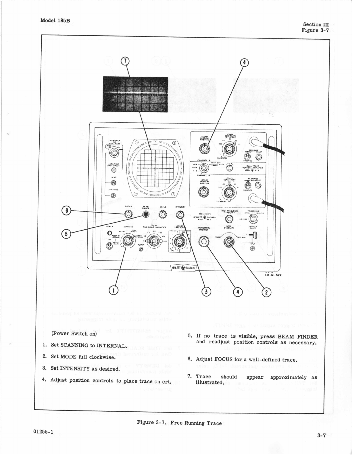
Model
185B
Section
Figme
111
3-7
P
I'
(Power Switch on)
1.
Set SCANNING
2.
Set MODE full clockwise.
3.
Set INTENSITY as desired.
4.
Adjust position controls to place trace on crt.
01255-1
to
INTERNAL.
Figme
5.
6.
7.
3-7.
Free Running Trace
If
no trace
and readjust position controls
Adjust FOCUS for a well-defined trace.
Trace should appear approximately as
illustrated.
is
visible, press BEAM FINDER
as
necessary.
3-7
Page 31

Section
Figure
III
3-8
I
!'
I
!
I
I
1
Q
P
Model
185B
..
I
I
I
!
i
i
L
Follow
1.
Connect trigger signal to trigger INPUT.
2.
Set
3.
Set
4.
Connect probe to signal to
If delay
to figure
instructions in figure
TIME SCALE MAGNIFIER
TRIGGER SLOPE as appropriate.
is
required (paragraph 3-17), refer
3-10.
3-7.
to
be
viewed. Note:
XI.
6.
Set
MODE
while maintaining reliable triggering.
7.
Adjust
amplitude.
8.
Set TIME SCALE as desired
CAL for calibrated time scale).
9.
Set
DENSITY as
while maintaining minimum flicker.
as
far
counterclockwise as possible
SENSITIVITY for the desired
far
clockwise
(set
VERNIER to
as
signal
possible
5.
Set TRIGGERING
trigger frequency and amplitude. presentation.
3-8
as
required, depending on
Figure
3-8.
1O.H
Unmagnified Trace
necessary, adjust STABILITY for
stable
01255-1
Page 32

Model
185B
P
Section
Figure
III
3-9
Follow instructions in figures
1.
Turn TIME SCALE MAGNIFIER clockwise
about four ranges (depending on amount of
magnification desired).
2.
Rotate TIME SCALE MAGNIFIER andDELAY
clockwise until the desired portion of the trace
01255-1
3-7
and
Figure
3-8.
3-8.
Magnified Trace
becomes visible. Adjust DELAY
to center the display.
3.
Adjust SENSITIVITY and VERTICAL POSITION
to
amplify and center trace.
4.
Finally, adjust TIME SCALE MAGNIFIERand
DELAY
to
achieve desired magnification.
if
necessary,
3-9
Page 33

Section
Figure
III
3-10
Model
I
l85B
P
Follow instructions in figure
Connect
tem as illustrated above.
Note: Be sure
nated to prevent reflection which would result
in misleading indications.
2.
Connect resistive divider probe to signal to
be
viewed.
3-10
185B
that
to
system
3-7. 3.
'looA
is
Line
SYs-
properly termi-
Figure
3-10.
Set
TRIGGERING
trigger frequency and amplitude.
4.
Set MODE as far counterclockwise
while maintaining reliable triggering.
5.
Adjust SENSITIVITY as required. Note: Remember that signal
factor
of
1/2.
6.
Set
TIME SCALE as required.
7.
Set STABILITY for stable presentation.
Viewing Delayed Signal
as
required depending on
as
will
be
attenuated by a
possible
01255-1
I
Page 34

Model 185B
Section
Figure 3-11
111
____1i
'I I
Follow instructions in figure 3-7.
1.
Connect
tem
2. Connect input of sync take-off
3. Connect output of Model
to be triaaered. Note: If
more
be
Model
as
illustrated above.
th&
needed.
120 ns delay, the delay line
185B to
llOOA
llOOA
test
Delay Line sys-
to
trigger source.
to
test circuit
circuit
itself
will
has
not
Connect probe to signal to
Set
5.
6.
,.
8.
TRIGGERING as required depending on
trigger frequency and amplitude.
Adjust SENSITIVITY
Set
TIME
SCALE
Adjust STABILITY for
as
be
as
required.
required.
stable
viewed.
presentation.
4.
I
Figure 3-11. Using Delayed Trigger
01255-1 3-11
Page 35

Section
Figure
III
3-12
Model
185B
Follow instructions in figure
If
external triggering
1.
ger
to
INPUT.
2.
Set TRIGGER SLOPE as appropriate.
3.
Set CALIBRATOR
counter clockwise.
4.
Obtain delayed sync pulse for triggering ex-
ternal circuit from
this
nect
pulse to trigger circuit under test.
AND
SYNC
3-7.
is
desired connect trig-
SYNC PULSE
PULSE output, Con-
Figure
full
3-12.
5.
6.
7.
8.
Delayed
Connect probe
If
external triggering
ING
as
quency and amplitude.
If
external triggering
far counterclockwise
taining reliable triggering; otherwise MODE
should
Adjust SENSITIVITY for desired
amplitude.
Sync
be
Pulse
to
signal to
required depending on trigger fre-
full
clockwise.
be
viewed.
is
used, set TRIGGER-
is
used, set MODE
as
possible while
main-
signal
as
3-12 01255-1
Page 36

Model
185B
w
Figures
Section
3-13
and
III
3-14
Obtain desired presentation on crt.
ures
3-7
to
3-9.
1.
Connect
external
scanning signal to INPUT
See
Figure
fig- EXT SCAN. (Input: 0 volts places scan
left
3-13.
edge of crt;
2.
Set SCANNING
External Scan
(REAR
+12
to
EXTERNAL.
OF
1858
volts at right edge.)
)
at
Obtain desired presentation
ures
3-7
to
3-9.
1.
Connect X input
SCAN OUTPUT. (Output: 0 volts = left edge
crt;
+12
volts = right edge.)
01255-1 3-13
of
X-Y
on
recorder
crt.
See fig-
to
TIME BASE
Figure
3-14.
2.
Connect Y input of recorder
OUTPUT. (Output:
crt;
+1
3.
Set SCANNING
4.
If
it
is
set
of
Recording the Signal
SCANNING
with SCAN.
-1
volt = top edge.)
to
RECORD.
desired
to
scan more slowly
to
MANUAL and scan signal
to
CHAN
A
(or
volt = bottom edge of
or
B)
rapidly,
Page 37

I
Section
Figure
IV
4-1
Model
185B
1
r
c
'I
.
4-0
01255-1
Page 38

Model 185B
Section
Paragraphs 4-1 to 4-16
IV
1
SECTION
PRINCIPLES
4-1.
INTRODUCTION.
4-2. GENERAL. The Model 185B oscilloscope and
its
vertical plug-in unit form a samplingunit for mea-
suring
is
graphs
the information presented
4-3. This
tween the
more detailed circuit description. An understanding
of the following information should prove
effectively troubleshooting Model 185B.
4-4.
4-5. GENERAL.
4-6. Figure 4-1,
Model 185B, shows functional relationships of each
major
ing the relationship between functional groups, the
Model 187B Dual-Channel Vertical Amplifier has
been shown
4-7. INPUT CIRCUITS.
4-8. The input circuits accept the trigger
The controls provide
nals
trigger circuits also select whether triggering will
on the positive
4-9. --GATE GENERATOR.
4-10.
ator produces the basic timing pulse for Model 185B
time base circuits (ramp generator, comparator and
comparator blocking oscillator, and horizontal- scan
generator). Usually the ramp-gate generator
gized by input trigger signal; however,
run for certain applications. Maximum repetition
rate for basic timing pulse
200 nsec/cm and faster, but decreases in proportion
-'
to
200 nsec/cm, becoming about 5 kc at 10 lsec/cm.
Thus when trigger repetition rate
mum timing pulse rate, one timing pulse
for each trigger pulse; when trigger repetition
exceeds maximum timing pulse rate, trigger signal
is
(ramp-gate pulse) maintains a strict time relationship
to
input trigger frequency.
4-11. USES
gate pulse
voltage in time-base circuits, 2)
back network
is
extender
and calibrator
fast repetitive signals. The circuit description
necessarily complex; a thorough reading of para-
3-1
to 3-34 will prove helpful inunderstanding
in
this section.
brief
major
BLOCK DIAGRAM DESCRIPTION.
section.
of various frequencies and amplitudes. The
RAMP
discussion of the relationship
functional groups
a
simplified block diagram of the
For
purposes of clarity inunderstand-
as
a part of figure 4-1.
for
stable triggering from sig-
or
negative slope of the input signal.
GATE PULSE. The ramp-gate gener-
is
followed
an
signal,
is
it
may be
is
100 kc for time
selected time scale for time scales slower than
is
less than
counted down. In
input trigger frequency
OF
has
to
not shown in figure 4-1), 3)
circuits,
sidls.
all
cases, basic timing pulse
or
to
some submultiple of
RAMP-GATE PULSE. The ramp-
four
functions:
complete
4)
it
its
own
it
triggers
initiates
1)
it
initiates a ramp
it
is
used in a feed-
cycle (this feedback
the
delayed sync pulse
scales
is
generated
ramp-gate
be-
by
aid in
be
ener-
free
maxi-
rate
OF
a
IV
OPERATION
4-12. RAMP-GATE EXTENDER AND GENERATOR
CIRCUIT. The ramp-gate extender circuit increases
the duration of ramp-gate pulse, producing an
tended pulse whose duration
tween input trigger, ti, and moment just after sampling,
h.
control of ramp-gate extender circuit (for TIME
SCALE settings slower than 100 nsec/cm), the ramp
generator produces a linearly-rising voltage whose
slope
This ramp voltage
4-13. TIME-BASE CIRCUITS.
4-14. COMPARATOR. In the comparator circuit, the
ramp voltage
(a
horizontal-scan generator when SCANNING
TERNAL). When ramp voltage reaches coincidence
with horizontal-scan voltage at time t3, the comparator produces a pulse which triggers the comparator
blocking oscillator.
4-15. COMPARATOR BLOCKING OSCILLATOR.
time t3, the comparator blocking oscillator produces
four pulses: two (the sampler trigger and stretcher
trigger) initiate sampling action of plug-in, the third
is
used in horizontal-scan (staircase) generator, and
the fourth
voltage.
4-16. HORIZONTAL-SCAN GENERATOR. The output
of the horizontal-scan generator
the horizontal amplifier and, through TIME SCALE
MAGNIFIER switch, to the comparator. The mode
horizontal operation
SCANNING switch S203. There
operation:
a. INTERNAL: the scan voltage
staircase-voltage generator. The beam
across crt and appears as a series
b.
tioning potentiometer R255A (figure 5-17) which
brought out to front panel as SCAN control. The display appears as a spot which can be horizontally positioned at
c. RECORD: the scan voltage
charging voltage across capacitor C240. The beam
is
output may be taken from OUTPUT TIME BASE SCAN
connector 5202, and vertical output from OUTPUT
CHANNEL Aconnector
B connector 53.)
d. RESET OR EXTERNAL: the scan voltage
rived from
PUT EXT SCAN connector 5201. The RESET OR
EXTERNAL position also
Model 185B
Triggered by the ramp-gate pulse andunder
is
dependent on setting of TIME SCALE switch.
is
fed to the comparator.
is
step level
MANUAL: the scan voltage
swept slowly across face of
compared
in
staircase voltage generated by the
is
used
to
initiate the termination of ramp
is
will
by means of the SCAN control.
an
external source, applied through
is
used on RECORD.
is
dependent on time
to
horizontal-scan voltage
is
applied
determined by the setting of
are
four modes of
is
derived from
of
discrete points.
is
derived
is
derived from
tube.
(The horizontal
52
or
OUTPUT CHANNEL
is
used
to
reset trace when
is
is
at IN-
to
by
ex-
be-
At
both
swept
posi-
is
de-
IN-
of
is
01255-1
4-1
Page 39

Section IV
Paragraphs 4-17
to
Model 185B
4-28
rl
n
n
n
n
n
n
f3
Figure 4-2. Time-Base Determination
4-17. CALIBRATOR.
is
4-18. The calibrator
a.
A
pulse amplifier and pulse extender-shaper:
a
pulse from the ramp-gate blocking oscillator
amplified, extended, and shaped
which
connector. There
between signal applied to front panel TRIGGERING
INPUT and signal available at SYNC PULSE OUTPUT.
gered
sine wave for the duration of sync pulse.
ages from
depending on setting of CALIBRATOR AND SYNC
PULSE switch.
4-19. VERTICAL AMPLIFIER AND ELECTRONIC
4-20. The vertical amplifier amplifies
vertical plug-in unit, and applies amplified signal
vertical deflection plates of cathode-ray tube (crt).
The electronic switch provides switching action necessary for dual-trace operation of plug-in unit.
4-21. HOFUZONTAL AMPLIFIER.
4-22. The horizontal amplifier amplifies the partic-
ular horizontal drive signal
setting of SCANNING switch and applies
zontal deflection plates of the crt.
4-23.
4-24.
actual speed of the horizontal beam across the face
of
base in sec/cm. The time base of Model 185Bis
dependent entirely upon time advance, between successive samples,
deflection voltage
ods
slope of ramp signal (TIME SCALE control), and
by varying amplitude of horizontal-scan voltage to
comparator in relation to horizontal-scan voltage to
is
made available at SYNC PULSE OUTPUT
is
b.
A
pulsed 50-mc oscillator:
by
amplified ramp-gate pulse,
c.
A
dc voltage divider:
0
volts dc
SWITCH.
TIME-BASE DETERMINATION.
At
this point,
the
cathode-ray tube has no relation
as
to
are used
to
vary
made up of three circuits:
to
a fast-rise pulse
approximately a 120-nsec delay
this
circuit, trig-
puts
this
circuit provides volt-
to
1000 millivolts dc, the level
that
has been selected by
it
should be emphasized .that the
compared
the crt.
this
time advance:
to
some horizontal
In
Model 185Btwo meth-
1)
RAMP GATE PULSE
STAIRCASE VOLTAGE
(HEAVY
RAMP VOLTAGE
(LIGHT. LINE)
SIGNAL ON
CATHODE RAY TUBE
(DOTTED LINE)
TRIGGER AND
SAMPLED SIGNAL
(SOLID LINE)
out a 50-mc
signal
from
it
to hori-
to
the time
by varying
is
to
2)
4
n
n n
LINE)
horizontal amplifier
ting of TIME SCALE MAGNIFIER control).
4-25. Figure 4-2 shows
SCALE control (varying slope of ramp signal). Note
that
as slope decreases, more time elapses between
ramp-gate pulse,
dence between ramp and horizontal-scan voltage, t3
(t3
=
time at which input signal
sult
is
that
a greater part of
ered
between successive samples, giving more cycles
per centimeter
of Model 185B
will be discussed in more detail.
4-26.
4-27. GENERAL. Before detailed explanation of circuit operation
of the operation of tunnel diodes in Model 185B triggering and time-base circuits. Tunnel diodes in
triggering and time-base circuits have
modes of operation:
the diode oscillates
sociated circuitry, and
is
gered back
4-28. ASTABLE OPERATION. Figure 4-3A shows a
typical circuit consisting of a low-voltage source
which supplies bias current to the tunnel diode through
an inductor which acts as
during switching times.
junction capacity and stray capacity are indicated as
a capacitor across the diode (the total of
will
ing discussion). The diode
the E-I curve in figure 4-3A.
flows through the inductor and diode, in
diode voltage will rise from the origin toward point C,
its
on the knee of the E-I curve,
negative resistance region and diode current begins
to decrease. However, the energy stored in the inductor’s magnetic field prevents
TUNNEL
triggered into one state where
to
the
a. The external load
be
termed diode junction capacity in
b. When power
operating point.
(this
ratio
the
tl
and the time of voltage coinci-
to
the viewer. After basic operation
is
discussed, time-base determination
DIODE
is
attempted, there will be adiscussion
at
original
OPERATION.
1)
free running (astable), where
a frequency determined by
2)
bistable, where the diode
state.
a
is
is
applied to the circuit, current
As
diode
n
n n
.-L
is
determined
effect
constant current source
shown as R1; the diode
is
of varying TIME
is
sampled). The
the
input signal
it
stays until trig-
biased
by
two
this
capacity
the
at
point C on
is
basic
follow-
series,
voltages passes point B
the
diode enters
its
current from
I”
set-
re-
cov-
the
as-
.
and
its
4- 2
01255-1
Page 40

Model 185B Section IV
=
+0.2v
-12.6V
Paragraphs 4-29
to
4-35
TUNNEL
DIODE
CRI
fb,
-
A. ASTABLE
Figure 4-3. Tunnel-Diode Operation
so
decreasing,
current and inductor current flows into diode junction
capacity. Since diode junction capacitance
this difference current causes a sharp voltage
across the junction capacity and hence across the
diode. This voltage
E-I curve.
equals the current supplied from
source, and
the voltage across the diode exceeds the supply voltage. Since current through the inductor
only during switching, current
diode voltage
When diode voltage reaches point E, tunnel diode CR1
again enters
current
pacity
now begins over again.
time (time BD)
pacitance and peak current. Pulse width (time DE)
and hold-off time (time AB) are determined
inductor, diode resistance, and power source resistance. Assuming the inductor acts as a constant current source for
load resistance determines the slope of lines BD
and EA.
4-29. BISTABLE OPERATION. Figure 4-3B shows
a bistable circuit of the type used inModel 185B triggering circuit. In this case there
with
CR1
stable at
emitter of Q1 (or a negative pulse to the
current through Q1, and hence the tunnel diode current, will increase,
current knee of the curve, the tunnel diode enters
negative resistance region. Diode current therefore
begins
stant current source, however, and prevents current
from decreasing; the current difference flows into
the
rapidly to point
again to zero, diode voltage falls to
mains until
to
is
is
c. For
tunnel diode CR1 as part of
is
biased at point R on
to
junction capacity.
drop below Iv.
the current difference between diode
is
rises
rapidly to point D on
At
point
D,
diode conduction current
the
constant-current
so
the voltage stops rising.
starts
starts
its
again held constant, and diode junction
forced to discharge to point
a
large value of load resistance, pulse
to fall toward operating point C.
negative resistance region. Inductor
is
determined by diode junction ca-
the
times involved, the size
is
the
this
point.
If
a positive pulse
At
this
is
to decrease, and
A.
a
PNP
its
E-I curve, and
constant
The process
transistor
collector load.
is
fed
base),
As
the current passes the high
decrease. Transistor Q1 acts as
As
a
result, diode voltage
V,
then when the input pulse falls
a
negative reset pulse causes the current
U
the
where
small,
rise
the
time
ca-
rise
by
the
of
the
to
the
the
con-
rises
it
re-
is
its
CRI
TUNNEL
DIODE
LD-L-545
E. BISTABLE
4-30. The circuit described in paragraph 4-29 can
be
made monostable by increasing transistor current
to
a point where
a current greater than
CR1
is
stable at point W on the curve shown
4-3B. Momentarily reducing tunnel diode current
to
less than that shown at point T in figure 4-3B will
cause the tunnel diode to go through a cycle from T
to R to
W
4-31.
4-32. GENERAL.
4-33. The following discussion
the synchronizing circuits in Model 185B.
otherwise noted, all reference to “signal” in the following circuit explanation will refer to the triggering
pulse under discussion rather than the signal to
viewed.
the crt refers
zontal amplifier. Refer
figure 5-13 and figure 4-4 in the followingdiscussion.
4-34. TRIGGER INPUT.
4-35. The trigger signal
ING INPUT connector 5101. TRIGGERING
SlOl
on
(less
TRIGGERING the input trigger
gate generator.
greater than 150 mv and frequency below 100 mc.
this
through
before being passed to the ramp-gate generator.
In
to a count-down circuit before being passed to rampgate generator.
lator consisting of diode CR120, inductor L101, and
low-impedance bias voltage source R155, R156 (fig-
ure 4-5A)
S
to
until triggered by another pulse.
TRIGGERING
All
is
adjusted to one of three positions, depending
frequency and amplitude of input trigger.
a.
SENSITIVE: for small amplitude trigger
than 150 mv) below 100 mc. In this position of
b. NORMAL: for trigger signals of amplitude
position of TRIGGERING the input trigger passes
a
20-db attenuator consisting of R158, R159
c.
HIGH FREQ: for trigger signals above 100 mc.
this position
is
the
tunnel diode
its
peak current. In this case,
V
to
W.
The circuit
CIRCUITS.
reference
to
to
horizontal-scan voltage
the voltage at the input to the hori-
to
is
is
always receiving
in
figure
will
remain at point
deals
primarily with
Unless
the schematic diagram,
connected
to
TRIGGER-
switch
signals
is
passed
of
TRIGGEFUNG, trigger
A
free-running tunnel diode oscil-
used to count down the input frequency
to
the ramp
is
applied
be
to
In
01255-1
4-
3
Page 41

Section IV
Paragraphs 4-36 to 4-38
to
approximately 10 mc. The trigger signal passes
through a trigger gate consisting of diode CR121,
CR122, and associated bias circuits. With no input
trigger, both CR121 and CR122 are conducting. The
current through CR121 passes through R152 from the
+12.6 volt source, while the current through CR122
passes through tunnel diode CR120. CR120 (with
L101) oscillates at a frequency around 10 mc with no
input trigger. (The basic operation of
this
circuit
is
explained in paragraph 4-26.) When an input signal
is
applied, CR121 and CR122 clip this signal. During
the positive clipping action, tunnel diode CR120
ceives pulses
CR122), and
rent knee
occurs, CR120
of
current (since
if
CR120
(see
figure 4-5B) when one of these pulses
will
is
near the top of
change
it
states.
is
in series with
its
Inductor L101,
re-
high cur-
HIGH FREQUENCY STABILITY, adjusts frequency
of CR120-Ll01 oscillator relative
so
that
an
input pulse
time relationship to
sists
of count-down circuit output pulses with a
will
always maintain the same
the
oscillator. The result con-
to
input frequency
fre-
quency near 10 mc, but synchronized with input signal.
4-36. RAMP-GATE GENERATOR CIRCUITS.
4-37. PULSE GENERATOR. The output of trigger
mode selected
is
fed to TRIGGER SLOPE switch S102
Model 185B
through transformer T101. S102 determines polarity
of signal
lecting triggering on either positive or negative
to
pulse generator Q104-Ql05-CR116,
se-
slope.
Transistors Q104 and Q105 are connected as adifferentia1 amplifier which triggers tunnel diode CR116.
This circuit constitutes a pulse generator whose
quency
is
determined
by
input pulses and/or hold-off
fre-
multivibrator V101B/V102AB (described in paragraph
4-41). The pulse generator circuit
operating
states
as
set
by
MODE control:
GER, a state where circuit must
input circuit
in
order to generate pulses,
has
two
1)
be
triggered from
basic
TRIG-
and
2)
FREE RUN, where circuit generates :pulses whose
frequency
is
determined by hold-off multivibrator
V101B/V102AB (figure 4-4). Resistor R160, MODE
control, and R157, Free Run Adjust, determine basic
operating state by adjusting current through Q104
which furnishes tunnel
diode
bias current;
this
is
equivalent to adjusting point R, figure 4-3B.
4-38. The circuit operates
MODE
trigger signal
switch S102
is
set
so
that
circuit must be triggered): Input
is
applied to Tl01.
is
in the + position, signal will be fed
through TlOl primary (since TI01 secondary
shorted, primary presents a very low impedance
signal)
to
base of Q105. IfSlO2isset in the - position,
as
follows (assuming
If
TRIGGER SLOPE
is
to
d
4-4
+
12.6V
Figure 4-4. Triggering-Circuit Block Diagram
ID.L.8U
01255-1
Page 42

Model 185B
A*.
:
C135 CR121
TRIGGER
SIGNAL
IN
R152
i
CR122
'io
TRIGGER
OUT
CR120
TUNNEL
DIODE
I
1
THIS
I
CR120
I
STATE
PULSE
CAUSES
TO CHANGE
Paragraphs 4-39 to 4-44
Section
IV
TRIGGER
SIGNAL
-
-
~~~
Figure
operation depends on frequency of trigger signal. For
high frequencies,
base
of
effective and signal
case,
base of Q105
actuate triggering circuits.
4-39.
Q105,
sulting positive pulse
emitter coupling capacitor, C145. The increased positive voltage at emitter of Q104 increases conduction
in
(figure 4-3B), tunnel diode CR116 switches
voltage stable
remains
vibrator (paragraph 4-41). (Any further trigger pulses
occurring before reset
The
entiated
4106, and fed to ramp-gate blocking oscillator Q107
through CR131. CR131
Q107
Q105. For low frequencies TlOl becomes
this
circuit must have either a positive pulse
If
a
positive pulse
its
emitter becomes more positive. The
that
element. When 4104 current increases
until
result
is
by
to
negative pulses.
signal
or
a negative pulse
state
reset
a
positive voltage step which
C146 and R178, amplified and inverted
is
coupled through TlOl
is
applied to base of Q104.
is
applied to the
is
coupled
(see
paragraph 4-29), where
by
a pulse from hold-off multi-
will
have no effect on CR116.)
limits
signal at the base of
4-5. Tunnel-Diode Count-Down Circuit
to
in-
In
any
to
to
base of Q104
base
to
of
re-
to
Q104 via common
to
IP
to
its
high-
it
is
differ-
by
VOLTAGE INCREASING
4-4L HOLD-OFF MULTIVIBRATOR. The ramp-
gate pulse coupled by T103
and R186, then delayed
is
then fed through CR107 where the negative spike
is
clipped off and the positive spike
hold-off multivibrator (V101B/V102AB). With a positive spike on
VlOlB. Hold-off multivibrator V101B/V102B remains in
and
all
circuits have had time to recover. The exact
hold-off time
switch S202 and
4-42. When V101B/V102B switch
mer
states
resulting negative voltage, coupled by capacitor C115,
back-biases diode CR124 and forward-biases CR125.
In
this
condition of the circuit, capacitor C115 now
effectively in parallel
current from the diode. Current through the diode
drops below I, (figure 4-3B) momentarily, returning
CR116 to
mains until another input trigger
its
this
state
is
determined by settingof
(VlOlB conducting, V102B cut
its
low-voltage stable point where
1
grid, V102B conducts, cutting off
until
after
by
setting of STABILITY control.
with
-
0.
is
differentiated by C155
psec by DL101. The pulse
is
sample has been taken
back
tunnel diode CR116, diverts
is
received.
W-
I-
305
applied to
TIME
to their for-
SCALE
off),
it
the
the
re-
4-40. RAMP-GATE BLOCKING OSCILLATOR. Transistor 4107 produces
pulse of about 1.5 psec duration. This
gate pulse and
a. To supply a gating
b.
To supply trigger
circuit.
c.
To provide trigger
d. To generate
in pulse generator
pletes cycle
In
order
ation of the reset pulse
01255-1
it
has
by
which ramp-gate pulse
to
simplify the following discussion, gener-
a
typical blocking-oscillator
four functions:
signal
signal
signal
a reset
pulse for tunneldiode CR116
circuit.
is
the ramp-
to ramp-gate diode.
to
ramp-gate extender
to
calibrator.
This reset pulse com-
is
produced.
will
be discussed
first.
4-43. There
reset
turned on. Also, under large signal conditions the
reset
pulse may
these reasons, an auxiliary reset oscillator
sures resetting of CR116 to the low-voltage
included in the triggering circuit.
4-44. Basically,
cuit consists of a voltage-sensitive switch (four-layer
diode CR111) with a small load, R135, that
tively coupled by C126 across the diode. Resistor
R134 and the -100 volt supply constitute
source for the circuit.
to
is
a possibility that CR116 may not be
the
low-voltage state when Model 185B
be
overcome
the
auxiliary
by
a
large trigger. For
reset
oscillator
that
state
is
capaci-
a
current
is
as-
is
cir-
4-5
Page 43

Section
Paragraphs 4-45
IV
t
IOOV
to
4-51
WQIO3
t
IOOV
Model 185B
Wo103
TI03
@
(iiJ
CR136
-
03
-
CURRENT DURING WAITING PERIOD
-
Jl!
+
..
IOOV
A
CR137
CR201
R210
Figure
CR207
0205
R212
-
---
CURRENT
CURRENT DURING EXTENDED RAMP
4-6. Ramp Generator
DURING
RAMP
e
GATE
A
+TO
!IL
CR207
8
0205
OF
so-
S202
I-
we
.
4-45. When Model 185B
through R134. When voltage across C126, and therefore across the diode, reaches about 20 volts, CRlll
conducts and quickly discharges C126. The circuit
delivers
a
second which
brator V101B/V102AB.
4-46. RAMP-GATE EXTENDER AND GENERATOR
4-47. The ramp-gate pulse
the
is
various dc currents
circuit.
4-48. Figure 4-6 shows dc current paths during
phases of
period (after end of last sample and before occurrence
of next trigger), current (figure 4-6A) flows from
+lo0 volt and +250 volt sources into both delay
erence-voltage source (Q2Ol-0202) and -100 volt
supply. Since diodes CR136 and CR201
ing, points
tial
The voltage (point C) at which ramp
low-impedance reference-voltage source Q201-Q202,
and DELAY control R212
Adjusting DELAY control R212 therefore sets voltage
at points
a
20-volt pulse
is
CIRCUITS.
ramp-gate extender circuit, Before
discussed, however, we should understand
Model
(disregarding forward potential of
A,
185B operation. During the waiting
A,
B, C, and D are all at
B,
C, and D.
is
turned on, C126 charges
2
p
seconds wide about once
used to trigger hold-off multivi-
is
also used
to
this
trigger
circuit
the
that
flow in the T103 secondary
all
ref-
are
conduct-
the
same poten-
the
diodes).
is
set by
on Q201-Q202.
adjusts
How
starts
bias
this
voltage affects
the
operation of ramp-gate extender and ramp-volt-
age
generator circuits
4-49. Transistors QlOl and Ql02 constitute rampgate extender multivibrator. This circuit
stable multivibrator with
500 ms; however, in actual operation
determined by length of time between input trigger
and moment of sampling.
4-50. When ramp-gate pulse occurs,
negative-going pulse from pin 7 of T103 causes Ql02
to
go to cutoff, forcing Q101 into conduction. When
Q102 cuts
increasing conduction
Q103, and therefore the anode of diode CR137
become more positive,
4-51.
gate pulse
step b)
(figure 4-6B)
anode of CR137 now
tential.) Diode CR201, suddenly back-biased, cuts
off, depriving point C of
this
source for a capacitor in the TIME SCALE switch.
The result
switch begins to charge up toward +250 volts through
R210 and R211, and the level
This
off,
its
At
the same time,
at
pin 6 of T103
causes
to
happens, +250 volts and R210 form a current
is
that
rising
voltage
is
discussed below.
is
a
mono-
a
period of approximately
its
period
the
resulting
collector becomes more positive,
in
Q103, causing emitter of
the
positive-going ramp
(see
paragraph4-40,
the
voltage at A and therefore
become positive. (The cathode and
are
at very nearly the samepo-
its
path
to
-100 volts. When
the capacitor
is
the ramp signal.
at
point C
in
the TIME SCALE
starts
to
at
rise.
is
to
B
4-6
01255-1
Page 44

Model 185B
Paragraphs 4-52 to 4-64
Section
IV
Note
The ramp signal
the outset due to the initial drop acrossR211
(see waveform
ing voltage of the ramp signal depends onthe
output of delay reference-voltage generator
Q201-Q202.
4-52. Meanwhile, the 1.5psec ramp-gate pulse
to
gins
continue
has
the
100 psec/cm the ramp-gate pulse must be extended.
The circuit accomplishes
When
value than the anode of CR137, CR137 begins conduction, and the Q103 emitter voltage
B*
changes
a
on CR201* (The ramp-gate extender multivibrator
does not change state until,
pling, the ramp
oscillator Q208-T203 reaches the base of transistor
QlOL
causes transistor
conduction, which changes conduction through Q103.)
4-53. When
changes
sends a pulse to trigger
The reset blocking oscillator then
the
the
negative, back-biasing CR137. The junction of CR201
and R195, deprived now of positive voltage through
CR137. returns
of DELAY, and conduction begins again through CR201.
The circuit
remains
from the ramp-gate blocking oscillator.
4-54.
4-55. Up
cuit
a
linearly rising ramp
front panel. We will now discuss
and how
age to produce a gating (sampler) trigger for the vertical Plug-in unit. Refer
(schematic diagram) in the following discussion.
4-56. COMPARATOR.
4-57. THE RAMP. To understand the method
achieving changes in time
understand the ramp and
and horizontal-scan circuits.
ramp voltage reaching coincidence
tal-scan voltage at time t3.
4-58. Referring
the ramp
decay. The ramp voltage at C, however, must
to
rise
been
longest
time
ramp-gate
However,
state,
heavily-conducting Q103
positive
bias
at
reset
The trailing edge of the ramp reset pulse
the
state
it
does
capacitor
ramp*
TIME-BASE
that
circuit
be
varied
in
2,
It
is
now at
triggered again
to
this
resets itself (the ramp-gate pulse generator),
for
e*ending
it
is
compared with the horizontal-scan volt-
tl,
then any voltage along the ramp can
makes
at
C,
Since
ramp-gate
the
at
an initial jump
figure 4-6B). The
asampleofthe
ramp
must
be
for
time
this
“extension”
A
drops
to
a
more
is
extender
coupled to point
start-
input
as
longer
as
follows:
negative
at
signal
long
maintain
point
B,
maintaining
after
the moment of sam-
pulse from comparator blocking
Qlol
to cut off, biasing Q102 into
ramp-gate exhder multivibrator
two
things
reset
TIME
simultaneously:
blocking oscillator Q203.
SCALE
emitter
to
a level determined by the setting
its
“waiting period”, where
the
CIRCUITS.
point we have discussed a pulse
this
whose starting
a
to
figure 4-7 and figure 5-17
base,
its
relation to the comparator
Figure
to
figure 4-8,
if
the
back
fires,
discharging
switch,
Of
we call the
terminating
‘lo3
to
ramp-gate pulse
and
(DELAY)
this
ramp voltage
it
is
essential
4-8 shows the
with
a
dc horizon-
more
“‘tage
On
start
be-
as
than
bias
1)
cir-
the
be
It
it
of
to
of
assigned a time value, depending on how long
the ramp
can
corresponds
4-59. Now
requires some kind of voltage-sensitive device. The
comparator
to
the desired point in time
comparator, and when the ramp reaches that voltage
(coincidence), the comparator
signal triggers the sequence which causes a sample
of the input signal
voltage which corresponds
is
the horizontal-scan voltage.
4-60.
is
steepened (dotted line) coincidence occurs sooner;
that
ramp
The cumulative effect of steepening the ramp
in
figure 4-2. The relationship of fie horizontal scan
to
the circuit and the ramp
more thoroughly in paragraph 4-66.
4-61.
a
diiferential
with
of
~205 exceeds the base voltage of Q206, which
the condition under which coincidence occurs, the
fast
goes
is
dependent
Q205 exceeds the base voltage of Q206; inother words,
the
circuit
4-62. The particular horizontal-scan voltage being
used,
voltage
This Q206 base voltage. then
horizontal position of-&e spot
poses of this explanation, assume the spot
extreme left of the
4-63. The horizontal-scan voltage for the comparator
a
is
brought through an attenuator, TIME SCALE MAGNIFIER switch S201.
clockwise and TIME SCALE MAGNIFIER set to
(the no attenuation setting), the voltage at the base of
Q206
therefore the emitter of Q205)
tive.
the base of 8205
by delay reference-voltage generator Q201, Q202,
and CR207. Negligible current flows through Q205
at
this
diode CR209.
4-64. When the ramp-gate pulse occurs, the ramp
takes
Q205
the ramp voltage on the
until the Q205 base voltage exceeds the base voltage
of Q206, and Q205 conducts. Conduction of Q205
to
reach that voltage. From
see
that
any voltage along a ramp of given slope
to
a specific time value.
to
pick
out
a point in time along the ramp
is
just
this.
A
voltage which corresponds
is
fed to one side of the
fires.
to
be
taken. In Model 185B, the
to
the desired pointintime
Note
in
figure
is,
less
time
(trigger
COMPARATOR.
its
rise
negative
resultant
time) and coincidence (sampling time),
amplifier
collector
produces
time.
with
on the length of time the base voltage of
pulse
operates
or
a
voltage
in
use,
is
approximately 0 volts, while
Before generation
time, and no current flows through tunnel
its
initial voltage step, and the voltage on the
base
rises to -0.2 volt.
4-8, that when the ramp slope
elapses
As
Soon
respect
The
duration
lasts
as
follows~
proportional
is
always present on the Q206 base.
between
The
with
a
Any
a
voltage
as
the
to
the
of
until
the
crt
about
With DELAY set
the
tunnel
diode
time
the
step
base
Qzos
the
resultant
ramp
to
the
horizontal-scan
is
proportional to the
on
the
to
start
its
is
slightly more nega-
of
is
the ramp voltage, however,
held at aDDroximately
After
the initial spurt,
base
of Q205 rises linearly
it takes
this,
then we
The resulting
start
of
the
is
shown
is
covered
is
essentially
in
series
base
voltage
is
having a very
of
Q205
again
base,
the
step
pulse
is
is
reset.
crt. For pur-
full
emitter(and
is
on the
a sweep.
counter-
-0.9
volts
The
X1
01255-1
4-7
Page 45

Section
Paragraphs 4-85 to 4-87
IV
RAMP RESET TRIGGER PULSE
iy-
RAMP-SATE
EXTENDER
MULTIVIBRATMI
t
250VF
I4
RAMP
RESET
PULSE
1
FIT
RAMP RESET
r
PULSE
AMPLlf
IER
TRIGGERS
TO
SAMPLING
PLUG-IN
-
f
fm
TUNNEL
DIODE
220K
R255A
I
STAIRCASE
RESET
BLOCK.
OX.
Model 185B
I-
I
I-
I
I
1-
DELAY
REFERENCE
SENERATOR
Figure 4-7. Time-Base Block Diagram
marks the time of coincidence. The resulting current
through Q205 and CR209 exceeds IP (figure 4-3),
CR209 changes
age across CR209
4-65.
As
pulse from CR209
reset
ramp
Meanwhile the horizontal-scan generator has stepped
the
Q206 base voltage
the actual step amplitude depending on the setting of
SCAN DENSITY. When the next trigger arrives the
ramp again
and then
the
with
the process continues until a horizontal sweep
completed.
base
that
rises
voltage
state
(paragraph 4-29), and the volt-
rises.
mentioned above (paragraph 4-61),
(the
blocking oscillator Q203 resets the ramp.
takes
linearly (this time alittlefarther) until
of Q206. The comparator
comparator pulse) lasts until
to
a
slightly more positive value,
its
initial voltage step
or
4205 again reaches coincidence
fires
to
-0.2 volt
again, and
this
is
a. The time scale in sec/cm
by
the TIME SCALE switch when no attenuation
RAMP
VOLTAGE
I
tl
5'
TIME
Figure 4-8. Ramp Voltage vs Time
I
t3
-
is
the value selected
G-S-554
I0-L-m
is
I
4-66. TIME SCALE/MAGNIFIER RELATIONSHIP.
4-67. The following discusses why time
pendent only on the slope of the ramp (determined by
the setting of TIME SCALE) and attenuation of the
horizontal-scan voltage (determined by the setting
of TIME SCALE MAGNIFIER). There
portant p9ints
TIME SCALE/TIME SCALE MAGNIFIER relationship:
4-8
to
remember when thinking about the
scale
are
is
de-
two im-
inserted (by TIME SCALE MAGNIFIER and/or
VERNIER) between the scan voltage at the input
the horizontal amplifier and the scan voltage applied
to
the base of Q206 in the comparator.
b. Any particular level of voltage applied
scan-voltage side
represents a particular point in time (paragraph
4-58), as measured from the startof the ramp. Therefore any change in the voltage applied to the Q206
(base
of Q206) of the comparator
its
to
to
the
01255-1
Page 46

Model 185B
base
will
(or
to
the comparator
SCALE MAGNIFIER
VERNIER
in sec/cm
TIME SCALE switch.
4-68. A voltage change of say
amplifier causes the spot to shift a certain number
of centimeters on the crt. Also, as described in
paragraph 4-67, step b,
comparator represents
4-69. Thus
pen sooner
cidence represents
also cause a change
curs when the ramp slope
ing TIME SCALE) or when horizontal-scan voltage
to the comparator
TIME SCALE MAGNIFIER).
4-70. Changing scan density, however, does not change
time scale because the horizontal-scan voltage
to the crt and the horizontal-scan voltage to the com-
parator are changed by the same ratio.
time scale can result only from a change in the slope
of the ramp signal
voltage applied to the comparator with respect to the
horizontal-scan voltage applied to the crt. Scan voltage as such has absolutely no effect on time scale (to
check this, switch SCANNING to MANUAL, and adjust
SCAN). Time scale can be expressed mathematically
as
follows:
ramp slope, attenuation crt deflection
(
where
attenuation factor
attenuated scan voltage (at comparator)
scan voltage at horizontal amplifier input
4-71. DELAY CIRCUITS.
4-72. As mentioned previously (paragraph 4-48),
the DELAY potentiometer determines the starting
voltage of the ramp signal by controlling the output
voltage of delay reference-voltage generator Q201Q202.A certain amount of delay
DELAY
sition). This delay insures
will have reached the linear portion of
istic before the
delay (the time between input trigger and
ple)
4-73. The following facts must
thinking about delay:
a.
occurs (plus
b. Any time lapse between the input trigger and the
first
cause the ramp to reach coincidence sooner
later)
in time. Thus when the scan voltage applied
is
is
ANY
so
sec/v
crt
deflection sensitivity
v/cm deflection
is
full counterclockwise (minimum delay po-
is
adjusted with MINIMUM DELAY, R213.
The ramp signal begins when the input trigger
a
comparator coincidence
is
attenuated (as
is
at any setting except CAL), time scale
no longer the value selected by the
at any setting except
x
this
same voltage sent to the
a
certain point in time.
method of making coincidence hap-
that from the
a
is
or
time scale in sec/cm
)
(
=
start
shorter interval of time
in
time scale. This
is
made steeper (by adjust-
further attenuated (by adjusting
a
change in the horizontal-scan
factor ) (sensitivity,v/cm
=
at
input to horizontal amplifier
that
first
coincidence occurs. Minimum
delay inherent in the circuit).
is
it
is
when TIME
X1
or
volts to the horizontal
of the ramp to coin-
is
what oc-
A
change
=
is
added even when
the ramp voltage
its
character-
first
sam-
be
remembered when
interpreted
as
delay.
its
will
in
I
Paragraphs 4-68 to 4-79
is
c. Time scale
amplitude difference between the signal to the comparator and the signal to the horizontal amplifier.
Differences in step-to-step amplitude of the staircase
(horizontal-scan voltage), nonlinear scan voltages,
etc, have no effect on the time scale.
4-74. Figure 4-9 shows the effect of varying the ramp
starting voltage. Unless TIME SCALE MULTIPLIER
is
on
X1,
DELAY control R212. When TIME SCALE MULTIPLIER
of delay available
tained by adjustment of screwdriver-adjust MINI-
MUM
or MINIMUM DELAY varies the output delay reference-voltage generator Q201-Q202, and hence the
ramp starting voltage.
4-72,
to avoid possible nonlinearity
The exact amount of delay which will occur depends
on two factors:
ing voltage was made negative (by either R231, MINIMUM DELAY or R212, DELAY), and
of the ramp.
4-75. DELAY/TIME SCALE MAGNIFIERRELATIONSHIP. When TIME SCALE MAGNIFIER
setting except
the horizontal amplifier and the comparator.
tenuation
signal-to-comparator and horizontal-signal- to-crt
decreased which decreases the time scale
on the crt. For example, with TIME SCALE
MAGNIFIER
displayed by the crt
is
at X1.
By means of the DELAY control, anydesired
fraction of the interval selected with TIME
SCALE can be viewed
gardless of the degree of magnification selected, effectively the crt can be moved along
the entire interval set by TIME SCALE by
operating DELAY.
4-76. Note in figure 5-17 (time base schematic diagram), and figure 4-7, that
MAGNIFIER
voltage generator circuit (Q201-Q202). This assures
that, regardless of the expansion used, the DELAY
control will always have the range necessary to permit observation for the entire time selected by the
TIME SCALE control.
4-77. COMPARATOR BLOCKING OSCILLATOR.
4-78. AMPLIFIER. The comparator pulse
entiated and amplified by C228-R231/232 and ampli-
fier Q207, respectively. The resulting negative spike
is
transformer-coupled to comparator blocking oscillator Q208-T203. Diode CR210 limits input to Q208
to negative pulses.
4-79. BLOCKING OSCILLATOR, These negative
pulses trigger blocking oscillator Q208-T203 and a
the ramp starting voltage
is
on X1, DELAY
DELAY, R213. Adjustment of either DELAY
a
small amount of delay
is
determined by ramp slope and the
is
is
1)
the degree to which the ramp start-
X1,
increased, the ratio between horizontal-
at
X10, only 1/10
as
is
associated with the delay reference-
inoperative, and the range
limited to that which can be
As
explained in paragraph
is
built into the circuit
in
the start
it
inserts attenuation between
as
when TIME SCALE MAGNIFIER
Note
much of the signal
at
one time and, re-
a
part of TIME SCALE
Section IV
is
varied with
of
the ramp.
2)
the slope
is
as
is
ob-
at any
As
at-
is
viewed
is
differ-
01255-1
4-9
Page 47

I
Section
Paragraphs 4-80 to 4-83
IV
TRIGGER
NO
DELAY DELAY
Figure 4-9. Effects of Delay
\
I
I
I
I
I
I
I
:
I
/FIRST
I
I
I
I/
I
Model 185B
SAMPLE
I.Y-8.e
pdse of about 1.3 kseconds duration
leading edge of
pulse triggers three circuits:
A
pulse, taken at pin 2 of T203,
a.
and fed via
trigger sampling gate circuits
b. Another pulse, taken at pin 4 of T203,
entiated and fed via
ates sampling action in the plug-in. When viewed on
an oscilloscope, this pulse often appears double,
the second pulse is actually feeding back from the
vertical plug-in unit.
c. Another output (pin
of the staircase voltage (paragraph 4-81).
4-80. In addition, the trailing edge of the comparator
blocking oscillator pulse
gate extender multivibrator, which
ramp (paragraph 4-52).
4-81.
4-82. The horizontal circuits
both to deflect beam on the crtand to provide scanning
potential for comparator circuit.
4-83. UNITY GAIN AMPLIFIER. V201A-Q210 constitute a unity gain amplifier. Tube V201A and transistor Q210 amplify the signal, while CR220 provides
dc coupling between the two elements. R270, the
Staircase Balance adjustment, sets the beginning of
the horizon.ta1-scan signal
plifier
drive except EXTERNAL. The four types of horizon-
tal
from voltage divider R254, R255, R256, and connects
it
HORIZONTAL-SCAN CIRCUITS.
is
used on all modes of operation of horizontal
drive selected by ,3203 (SCANNING) follow:
a.
RECORD. In RECORD, S203 disconnects C240
to the grid of V201A. C240 charges slowly toward
this
comparator blocking oscillator
J1
to the sampler unit where
J1
to sampler unit where
1)
is used in the generation
is
used to reset the ramp-
in
at
is
produced, The
is
differentiated
it
is
used
in
vertical plug-inunit.
is
differ-
it
initi-
in
turn resets the
Model 185B are used
0
volts. The unity am-
to
but
+lo0
volts through R259 until voltage at junction of
CR219
CR219 begins conduction, halting the sweep. The
charge on capacitor C240
until SCANNING (S203)
NAL. With ,3203
C240 discharges through resistor R257.
has
tor C240 as explained in RECORD, above, or
connects 5201, INPUT EXTERNAL SCAN connector,
through S203B, to comparator and horizontal amplifier
circuits,
drive these circuits. The external signal should
between 0 and approximately + 12
ZONTAL POSITION approximately centered,
puts spot on left-hand edge graticule,
puts spot on right-hand edge.)
except grid of V201A
R255A, SCAN (MANUAL),
manually control scanning.
amplifier V201A-Q210
results from the following circuit action (see figures
4-10 and 5-20):
and R259 reaches +15 volts. When
will
remain
is
set
at
RESET OR EXTERNAL, capacitor
b. RESET OR EXTERNAL. This position of S203
two uses:
c. MANUAL. Operation
d. INTERNAL. In INTERNAL, the output of unity
(1)
Prior to
ceding staircase), staircase capacitor C236
discharged, comparator blocking oscillator
(Q208-TZ03 which generates sampler trigger)
has not yet generated the next pulse, and diode
CR215 is back-biased.
(2)
When coincidence occurs, comparator blocking
oscillator Q208-T203 fires, and the resulting
pulse
CR215. CR215, forward-biased now, conducts,
and capacitor C236 begins to charge.
1)
it
is
used to reset charging capaci-
so
that an external signal may be used to
is
start
of circuit sequence (end of pre-
is
coupled by transformer T203 to diode
to RESET OR EXTER-
volts, (With HORI-
is
similar to RECORD,
connected to center arm of
so
that the operator can
is
a staircase voltage which
this
at
+15 volts
+12
occurs
2)
it
be
0
volts
volts
is
4-10
01255-1
Page 48

Model 185B
Section
IV
Paragraph 4-84
(3) The voltage across staircase capacitor C236
is
increases, and
applied, through SCANNING
switch S203C/D, to unity amplifier V201AQ210, increasing output of the generator by the
same amount;
this
output
is
the horizontal-
scan voltage.
(4)
After
comparator blocking oscillator pulse decays, diode CR215 becomes reverse-biased
again, and prevents charge on capacitor C236
from leaking off.
(5) DENSITY contrbl R255B
of
staircase capacitor C236. DENSITY per-
mits
limited adjustment of charge-path
ance, thereby determining amplitude
is
in the charge path
resist-
of
stair-
case steps by controlling amount of charge
added to staircase capacitor each time blocking oscillator
(6) The output
applied to transformer T203 in such a way
a
bootstrap action results. Thus for a given
density, the same amount
fires.
of
unity amplifier V201A-Q210
of
charge
is
is
that
added
to staircase capacitor C236 each time, which
results in staircase steps of equal amplitude.
(7) When voltage across staircase capacitor C236
reaches about +15 volts, reset blocking oscillator Q209-T204
pacitor. The staircase
fires
and discharges the ca-
is
thus reset and
starts
over again.
4-84. RESET BLOCKING OSCILLATOR. When the
staircase voltage exceeds voltage on collector of Q209
(approximately 15 volts), diode CR217 becomes for-
ward-biased, current begins to flow through collector
of
winding
fectively becomes the voltage supply for blocking
cillator Q208-T204. The effect
is
transformer-coupled to the base of Q209, which
transformer T204, and capacitor C236 ef-
os-
of
this
current flow
causes blocking oscillator to fire, essentially dropping collector of Q209 to ground. The resulting current-flow through CR217 and QZOQ discharges capacitor (2236, thereby resetting the staircase. It might
be
pointed out here that the amplitude of the staircase
signal remains constant. The height
ual step can
be
varied by adjusting R255B as mentioned in paragraph 4-83, step
varying the height
ber
of steps per staircase, which changes the number
of
each step
of
each individ-
d
(5). The result of
is
to change the num-
of samples per sweep on the crt.
8
1
L'Cg38
-FEEDBACK
1
RESET
BLOCKING
OSClLL
ATOR
0209
?hi450
lo.01
=
4R2tB
-12.6VF
R267
300
IR253
13.7K
t25OVF -IOOVF
1
R255E
30K
0
tC.,
DENSITY
52038
1
HORIZONTAL SIGNAL
tIOOVF
1
t
t12.6VF
r-----
OUTWT
TIME EASE
-'SA!!
J202
I
I
-
J
i
R272
L
I8K
c
r
so-,
TO
COMPARATOR
AND HORIZONTAL AMPL.
.I
Figure 4-10. Staircase Generator
01255-1 4-11
Page 49

Section
Paragraphs 4-85 to 4-100
IV
Model 185B
4-85. OUTPUT. The output of unity amplifier V201A-
is
Q210
4-61). The path from unity amplifier
the time scale VERNIER (or, when TIME SCALEvernier
through Sweep Calib adjustment R285, TIME SCALE
MAGNIFIER switch S201 where the staircase voltage
is
and
assembly A501.
4-86. HORIZONTAL AMPLIFIER. The horizontal
amplifier
amplifier. The scan voltage
the amplifier, the horizontal positioning voltage to
the other. The level of the positioning voltage is
with R509, the HORIZONTAL POSITION control. The
output of the amplifier
horizontal deflection plates of the crt.
4-87.
4-88. SYNC PULSE. When CALIBRATOR ANDSYNC
PULSE
is
negative pulse. When the ramp-gate pulse (paragraph
4-40, step c) appears on its base, Q60l saturates,
and
4-89.
ation. Capacitor C602 charges slowly through R604
and Q601, holding Q60l on for a time determined by
R604-C602 time constant.
4-90. Before ramp-gate pulse appeared on base of
Q601, CR604 was conducting and therefore presented
a
Q60l appears on its cathode, CR604 acts in
different manner than an ordinary diode. Instead of
immediately cutting off, reverse current flows momentarily, and the impedance
low (the reverse current
stored during the time the Q60l collector
+12
stops, and impedance of diode CR604 rises sharply;
because of this characteristic, diode CR604 provides
very
rise pulse. During the short period between back-
bias and cut-off, CR204 produces
step; diode CR603 blocks this step, and passes only
the steep-rise portion of the pulse.
4-91. The pulse, thus shaped by CR604 and CR603,
is
4-92. PULSED 50-MC AMPLIFIER. During the time
between pulses from amplifier Q601, the junction
€260’7 and R610
holding base of Q603 slightly negative.
4-93. When amplified ramp-gate pulse appears on
Q60l collector, CR605
described in paragraph 4-90) becomes back-biased.
When
fed:
a.
To one side of the comparator (see paragraph
is
through R286,
is
at
CAL, through contacts on switch S204),
attenuated
cathode follower V201B.
b. To the grid of V501B
if
S201
is
on any except the X1 setting,
in
horizontal amplifier
is
a
conventional, single-stage differential
is
applied to one half
set
is
connected directly to the
CALIBRATOR.
is
biased
very low impedance. When positive pulse from
coupled to J601, SYNC PULSE OUTPUT connector.
full counterclockwise, pulse amplifier Q60l
so
that
it
can conduct when triggered with
its
collector rises to
As
Q60l turns on, Q602 is driven into satur-
volts). Carriers are depleted abruptly, current
fast
switching action, and the result
is
slightly negative and CR605 conducts,
it
snaps off, resonant circuit T601-C610
+12
volts.
a
of the diode remains
is
supported by the carriers
is
is
a
small voltage
(a
diode of the same type
slightly
rising to
a
fast-
as
is
of
of
shock-excited
the tank-circuit losses, resulting in a constant-amplitude oscillation, and a 50-mc voltage
5602, the 50-mc connector. When the sync pulse ends,
CR605
nating the 50-mc oscillation.
4-94. DC CALIBRATOR VOLTAGES. The rest of
this
-12.6 volts and ground. The level of the voltage fed
to the AMPLITUDE DC OPEN CIRCUIT connector depends on the setting of S601, the CALIBRATOR AND
SYNC PULSE switch.
4-95.
4-96. GENERAL OPERATION.
4-97. Figure 4-11
amplifier. The signal under investigation
to the input of the vertical plug-in unit, and
to Model 185B vertical amplifier via pins on connector
J1
4-98. In the Model 185B vertical amplifier, input
signals are applied to cathode followers
a
V2,
Q3-Q4. Multivibrator V4 controls the differential
amplifiers
Thus only the signal applied to the “on” differential
amplifier
“off” differential amplifier blocks the signal applied
to
multivibrator V4.
4-99. CONTROL OF DIFFERENTIAL AMPLIFIERS.
Except while switching, one plate of multivibrator V4
is
explanation, assume the V4A plate
therefore diode CR1 between the plate of V4A and the
bases of Ql-Q2
the positive voltage on the V4A plate
bases of Ql-Q2, back-biasing their emitter-base
junctions, and Ql-Q2 are cut off.
the V4B plate
tween V4B and Q3-Q4, and amplifier Q3-Q4 operates
normally.
4-100. CONTROL OF MULTIVIBRATOR V4. When
the plug-in unit
fier, the vertical presentation switch (channel and
mode-of-operation selector) controls multivibrator
V4. The vertical presentation switch lock multivibrator V4 in one state or the other
channel operation, or allows multivibrator V4 to freerun to provide dual channel operation. Multivibrator
V4
dual channel operation, both differential amplifiers
are turned on some time during each sampling period
even when the instrument
sampling rate of 100 kc. To provide
display, the Model 187B simultaneously applies the
Channel
the Channel B signal to amplifier VlB, Vertical deflection on the crt
ence between the signal voltages.
is
circuit
(not shown in figure 4-11).
and then to differential amplifiers Ql-Q2 and
it,
positive
is
designed to free-run up to about 180 kc,
into
50-mc oscillation. Q603 overcomes
is
coupled
again clamped to a negative voltage,
is
simply a dc voltage divider, between
VERTICAL AMPLIFIER.
is
a
block diagram of the vertical
so
that
only one
is
amplified and applied to the crt. The
Circuits in the vertical plug-in unit control
and
the other negative; for purposes of
is
turned on
is
is
conducting. Under
is
negative, back-biasing diode CR2
is
the Model 187B Dual Trace Ampli-
this
is
At
the same time,
to
provide single-
termi-
is
applied
is
applied
V1
and/or
at
a time.
positive, and
condition,
applied to the
be-
so
is
running
A
signal to the Model 185B amplifier
is
then proportional to the differ-
at
its maximum
a
differential
V1A
and
to
in
4-12
01255-1
Page 50

Model 185B
-
4
OUTPUT
AMPLIFIER
v3
-
Section
Paragraphs 4-101 to 4-108
TO VERTICAL
DEFLECTION
PLATES OF CRT
IV
t
CATHODE CATHODE
FOLLOWER
VIA V2A
INPUT FROM
CHANNELA
OF PLUG-IN
4-101. TRANSIENTS.
4-102. To prevent switching transients from appear-
ing on the
brator V4
crt to blank the crt during switching time. During
sampling,
pulse to amplifier V5;
transients from appearing on the crt.
4-103.
4-104. The high-voltage power supply (figure 4-12)
provides voltage (-2900 volts) required to operate the
crt. An
mately 80 kc. High-voltage transformer T301 steps
up oscillator output
V303 and V304 and their associated rc filters convert
to
dc. The dc voltages are applied to the crt. Regulator V301 compares output of the
with +250 volts and changes amplitude of
tions to oppose any high-voltage change relative to
the 250 volts.
I
j
CATHODE CATHODE
FOLLOWER
VERTICAL
PRESENTATION
SWITCH
PLUG-IN
crt,
a
negative pulse generated by multivi-
is
applied to amplifier V5 and then to the
the
vertical plug-in unit sends a blanking
HIGH-VOLTAGE POWER SUPPLY.
rf
oscillator, V302, oscillates
to
a high
d
DIFFER-
ENTIAL ENTIAL
AMPLIFIER AMPLIFIER
01/02
MULTI-
IN
e---
VIBRATOR
-
Figure 4-11. Vertical Amplifier Block Diagram
this
pulse prevents sampling
at
ac
voltage which rectifies
crt
cathode supply
+=
v4
approxi-
rf
oscilla-
FOLLOWER
1L
1L
-
DIFFER-
03/04
4
*
FOLLOWER
V2B
-
e
BLANKING
PULSE
AMPLIFIER
v5
.
1
4-108. The series regulator in each supply acts as
a
variable resistor in
A
comparison or differential amplifier senses any
change in the output voltage by comparing the output
against a fixed reference voltage. The amplifier then
changes the resistance of the series regulator in
way
that
power supplies are transistorized. Emitter followers
are required between amplifier and series regulator
to amplify the current to the level required to drive
the series regulator.
opposes the change in output voltage.
n
BLANKING
-
b
PULSE FROM
series
AMPLIFIER
V301
PULSE
TO CRT
BLANKING
PLUG-IN
with the supply output.
BD-Y-273
INPUT FROM
CHANNEL B
OF
PLUG-IN
a
The
+250V
*
4-105. The
pulses from V5 (paragraph 4-102) blank the crt to
prevent undesirable transients from appearing.
4-106.
4-107. The low-voltage power supplies include one
independent supply and four dependent supplies. The
-100 volt supply
reference for the +lo0 volt and +250 volt supplies
and
is
of the +12.6 volt and -12.6 volt supplies.
01255-1
crt
is
normally biased on. Blanking
LOW-VOLTAGE POWER SUPPLIES.
is
the independent supply. It
a supply voltage for the comparison amplifiers
is
TO CRT
GRID
BLANKING-
a
Figure 4-12. High-Voltage Power Supply
PULSES
Block Diagram
2
.E
..*.,
4-13
Page 51

Section V
Table 5-1
Model 185B
Table 5-1. Recommended Test Equipment
Instrument
oscilloscope
DC Voltmeter/
Ohmmeter
Precision DC
Voltmeter
High Voltage
DC Voltmeter
AC Voltmeter Voltage Range: 10 mv rms
Variable
Transformer
“Qpe
Required Characteristics
Passband:
Sensitivity: 0.5
Input Impedance: 10 megohms
Voltage Range: 1-300 volts
Voltage Accuracy: 3%
Input Impedance:
Resistance Range:
Voltage Range: 10-300 volts
Input Impedance: at least 10 megohms
Accuracy:
Voltage Range: 3000 volts
Input Impedance: 12,000 megohms
Accuracy: 8%
Input Impedance:
Accuracy:
Output Voltage: 103-127 volts
(206-254 volt
wired for 230-volt operation)
Output Current: 5 amps (2.5 amps
for 230-volt operation)
dc
1%
10%
to
if
10 mc
to
100 volt/div
(with probe)
at
least
1
ohm
megohms
at
least
oscilloscope
10 megohms
to
20
1
megohm
Use
Observation of waveforms
General voltage and
sistance measurements
Set
low voltage power
supplies
Measure high voltages
Measure low voltage
power supply ripple
Vary line voltage General Radio
re-
Model
AN/USM-lOBA
@
150A
@
160B
@
170A
($9
175A
ME-26A/U
@
410B
@
412A
9
412A
TS-520/U
($3
410B with
@
459A
ME
-3
OA/U
@I
400D
Type
WlOMT3A
.
Signal Generator Frequency Range: 10-100 mc
Output Amplitude: 15-500 mv
Frequency Accuracy: 0.1%
Signal Generator
Pulse Generator
Delay Line
Sync Take-Off
Plug-In
Amplifier
bad,
50-Ohm
50-Ohm
-0
Frequency: 1000 mc
Amplitude: 20.7 mv
Rise
Time:
Amplitude: at least 50 mv
Delay: 120 nsec
Passband:
~
hput Impedance: 50 ohms
1O:l ratio Divider
I
Compatible with 185B
50-ohm Type
Qdapter to 187B Probe
Type
less
500
N
connectors
than 10 nsec
mc
N
connector
-
50-ohm
Check frequency calibrator
accuracy and trigger
sensitivity
Trigger sensitivity
Set minimum delay
Provide fixed delay
Split input signal into
two
~~ ~~
signals
Attenuate sync pulse
amplifier system
Terminate 50-ohm test
Signal
To insert probe in
50-ohm system
AN/USM-44A
@
608D
I
@612A
@J llOOA
($3
185A-76A
@
187B-76C
@
908A
@
187B-76E
01255-1 5
Page 52

Model 185B
Paragraphs 5-1 to 5-20
Section
V
SECTION
MAINTENANCE
5-1.
INTRODUCTION.
5-2. This section provides maintenance and service
information for Model 185B oscilloscope. Included in
this
section
to
verify proper instrument operation. The section
also includes recommended test equipment, troubleshooting, repair, and adjustment procedures.
5-3.
5-4. Table 5-1
to complete the maintenance instructions in
tion. Instruments other than those recommended may
be
used, provided their performance meets the basic
requirements given
5-5.
5-6. CLEANING THE AIR FILTER.
5-7. Inspect the
before
a. Remove filter from instrument
it
in warm water and detergent.
b. Dry the filter thoroughly and coat
adhesive,
search Products Company, Inc. This adhesive comes
in “Handi-Koter” sprayer cans and
most heating supply stores or from your authorized
Hewlett-Packard sales representative.
5-8. GENERAL MAINTENANCE.
5-9. Other than periodic cleaning of the air
as mentioned above, the Model 185B requires no spe-
cial preventive maintenance. We do suggest, however,
that low pressure air
dust out
5-10. CABINET REMOVAL.
5-11. To remove the Model 185B cabinet, proceed
as follows:
a. Remove the plug-in unit.
b. Set instrument on
Be careful of the probe clips.
c. Remove four screws at rear of cabinet.
d. Lift cabinet up and off the instrument.
5-1
2.
5-13. The troubleshooting procedure
two categories:
the trouble
the instrument, and
which trouble
is
a performance check which may
TEST INSTRUMENTS REQUIRED.
lists
test
in
table 5-1.
equipment
that
is
PERIODIC MAINTENANCE.
air
filter regularly, and clean
it
becomes dirty enough to restrict air flow.
rear,
it
with filter
We
recommended Filter Coat No.3 from Re-
is
available from
be
used to blow any accumulated
of
the instrument every
its
TROUBLES H OOTl
1)
system troubleshooting,
is
associated with a particular section of
2)
is
located within a particular section,
sectional troubleshooting, in
front-panel draw handles.
N
0.
six
months or
is
divided into
be
used
required
this
sec-
and wash
filter
so.
in
which
it
V
5-14. Since Model 185B cannot function without
vertical plug-in unit, system troubleshooting
on the assumption that a Model 187A or 187B Dual
Trace Amplifier unit
tional troubleshooting information on the plug-in unit,
refer to the instruction manual
5-15. SYSTEM TROUBLESHOOTING.
5-16. System troubleshooting consists of observing
indications on the crt and associating the indications
with a particular section or circuit.
indications are listed in table 5-2 along with any necessary steps for clarification. If
erating but does not meet all specifications, refer
the appropriate section of the performance check,
paragraph 5-67, and check the particular instrument
operation in question.
5- 17. SECTIONAL TROUBLESHOOTING.
5-18. MAIN VERTICAL AMPLIFIER. Since the ver-
tical amplifier consists of balanced amplifier circuits,
trouble other than open tube heaters will usually cause
an unbalance. If an unbalance
nels, check circuit of V3. Ifunbalance
nel only, short input of faulty channel to ground and
check voltages throughout the channel.
Troubleshoot vertical amplifier with ver-
tical
plug-in unit installed. Otherwise multivibrator V4
shooting more difficult. However,
traces appear on screen near center when
vertical plug-in
indication that trouble
5-19. TRIGGER CIRCUIT. Troubleshooting the sync
circuit
forms throughout the circuit are shown in figure 5-11
opposite the schematic.
5-20. The following
Model 185B trigger circuit.
sure that all diodes and transistors are mountedproperly on etched circuit board and that all power supply
voltages are within specifications (paragraph 5-47).
MODE full counterclockwise, collector voltage should
be approximately -12.5 volts, and should increase to
-5 volts as MODE
test
tunnel diode CR116.
voltage across CR116 with dc electronic voltmeter.
The anode to cathode voltage should be about 10 mw.
is
best
a.
Measure voltage at collector of Q104. With
indicates that bias current
b. Turn MODE full counterclockwise and measure
is
installed. However, for sec-
for
the plug-in unit.
the
instrument
is
common to both chan-
Note
will
free run and make trouble-
is
removed,
is
done by observing waveforms. Wave-
will
be helpful in troubleshooting
is
rotated to full clockwise. This
this
in
the plug-in unit.
First., of course, make
is
being supplied to
is
A
number
is
in one chan-
if
two
is
a good
based
is
op-
of
to
a
01255-1
5-1
Page 53

Section
Paragraph 5-21
V
Model 185B
Table 5-2. System Troubleshooting
Indication
Nothing visible on crt
with BEAM FINDER
pressed
Vertical unbalance, but
trace on screen when
BEAM FINDER
pressed
No vertical deflection
from either channel
but sweep
mately centered
No
vertical deflection
from one channel, but
operation of other
channel
Same channel on screen
regardless of channel
selected
Vertical troubles on
per-sample basis
(vertically elongated
samples, etc)
Hash on screen (no crt
blanking during sampling or chopping)
is
is
approxi-
normal
is
Action
Check low voltage power
supply, vertical amplifier output stage (V3),
horizontal amplifier
V501, high voltage
power supply, and crt
in
that order.
V1
7
to
is
of
Model
and V2
eachver-
If
present
If
Short grids of
2
(pins
tical amplifier input
stage)
vertical unbalance re-
mains, check vertical
amplifier. If trace
appears on screen
check plug-in unit.
Check V3 and V4 in ver-
tical amplifier, plug-in
unit.
Check input
185B from faulty channel of plug-in with a sig-
nal
If
check plug-in unit.
signal is present, check
vertical amplifier.
Check multivibrator V4
in vertical amplifier
Check plug-in unit
Check Peaking Adj in
v3
Check amplifier V5
Check blanking circuitry
and
to
ground.
applied to channel.
no signal
No trace but spot
screen and VERTICAL
POSITION and HORIZONTAL POSITION
controls operate
No trace but
visible (BEAM FINDER
may have to
HORIZONTAL POSITION control
tive but VERTICAL
POSITION
Sweep
free
MODE set
and no trigger signal
applied
Operation normal on
trigger repetition
rates below 100 kc,
faulty on trigger rates
above 100 kc
a
Horizontal unbalance
Horizontal troubles on
per-sample basis
(horizontally elongated
samples,
Excessive noise and
jitter which appears
sinusoidal
trigger repetition rates
is
spot
is
be
pressed);
is
effec-
is
not
runs with
to
TRIGGER
etc)
at
certain
Action
:heck
on
reset
oscillator Q209, unitygain amplifier V201A/
Q210 in time base
Check sync circuit
Check time base
circuit
Check blocking oscilla-
tor Q106/Q107 in sync
circuit, comparator
blocking oscillator
Q208 in time base.
Check Q104, Q105
Check hold-off multivi-
brator V101/V102
sync circuit
Check horizontal
amplifier
Check time base circuits
V201A and Q210, diodes
CR215, CR217 and Q205
Check low voltage power
supply
Be sure trigger
overdriving input
blocking
is
not
“two
is
If
if
does
to
full
the
the
c. Slowly rotate MODE clockwise. The anode
cathode voltage should increase to about 60 mv and
is
then jump to about 470 mv when MODE
o’clock’’. Continue turning MODE until
clockwise. The voltage should rise to about 500 mv.
d. Turn MODE full counterclockwise. The cathode
to
anode voltage should jump back to 10 mv.
anode to cathode voltage
voltage does not change
MODE full counterclockwise and flip power switch
off and on two or three times.
not change to about 10 mv, CR116
or out of specifications, and should be replaced.
5-2
is
as
about
MODE
500
If
voltage
is
near
it
mv, and
is
rotated, turn
still
either defective
5-21. If, after completing the above procedure, the
will
instrument
a.
Open the circuit loop by lifting C146
tion of R175 and L112 (see figure 5-1).
b.
Set controls on
lows (use 75-ohm source):
(1)
Attenuation
(2)
Amplitude
(3)
Frequency to 30 kc
c.
Using clip leads, connect equare wave generator
to
capacitor and to ground
not free
at
at
1
square
0
db
volt
run,
proceed
wave generator
as
shown in figure 5-1.
as
follows:
at
the junc-
01255-1
as
fol-
Page 54

Model 185B
Paragraphs 5-22
Section
to
5-28
V
A103
-TRIGGER
Figure 5-1. Driving the Trigger Circuit
CIRCUIT BOARD
TO
GROUND
LO-S-5Sl
should
left,
5-26.
on
the ramp-gate extender multivibrator
emitter of Q103 and the emitter end of resistor R147
from circuit board' (see paragraphs 5-34 and 5-37).
The Model 185B should operate on the four fastest
time-scale ranges. If
gate extender
5-27.
sync pulse circuit consists of a pulse extending amplifier Q60l/Q602, a 50-mc oscillator Q603 and
shaping diodes CR604/605. The waveforms for this
section are shown on figure 5-23. If both time calibrator and sync pulse are faulty, check Q60l and
Q602. If only the sync pulse
If
CR605 and Q603.
5-28. HIGH-VOLTAGE POWER SUPPLY. Measure
voltages supplied
be
less
than about 1 cm/sec. If spot drifts
check CR215;
If
time-base circuits
all
ranges and the cause
TIME
CALIBRATOR. The time calibrator and
the fault
Be very careful when measuring highvolt-
Use
ages.
measurements.
if
spot drifts right, check CR217.
are
operating erratically
is
not apparent, disable
by
it
does, trouble in the ramp-
is
indicated.
is
faulty, check CR604.
lies
only in the time calibrator check
to
the crt.
WARNING
equipment suited for high-voltage
lifting the
two
The square wave cannot
Q107. The observed voltages should appear essentially
as
Btor
scribed previously.
function properly when driven from the square wave
generator, but the tunnel diode
CR104, CR124, and CR125 for continuity and proper
polarity.)
5-22. Count Down Circuit.
not trigger on the high frequency count down circuit,
turn TRIGGERING to HIGH FREQUENCY and measure voltage at anode of CR120. This voltage should
be
with
and
10-mc sine wave, approximately 300 mv peak-to-peak.
If
voltage
served, change CR120 (read paragraph 5-36 before
attempting
6-23. TIME BASE. Troubleshooting the
best
5-24.
ates normally,
not Qiggered, V201A (excessive grid current) may
be
between samples. Set DENSITY
and carefully check waveform at Q210 collector for
sag
shown in figure 5-2. (The blocking oscil-
and hold-off multivibrator should operate as de-
about
200
a
Model 150A/151A
an
done
If
mv. Observe
AC-21C probe. The waveform should
is
correct, and the sine wave cannot
to
replace tunnel diodes).
by
observing waveforms
comparator blocking oscillator Q208 oper-
but
removing charge from staircase capacitor, C236,
between samples.
be
traced through Ql06 and
If
all
parts of the trigger circuit
will
If
the Model 185B
signal
or
a Model 160A oscilloscope
at anode of CR120
(see
reset
blocking oscillator Q209
full
counterclockwise
not reset, check
will
be
be
ob-
time
base
is
figure
5-15).
is
crt
a.
If
receiving a faulty blanking signal, replace crt.
b.
If
cillator V302
crt
cathode supply causes a greater output from the
rf
oscillator and therefore a more negative output
from the crt grid supply,
grid supply
both crt supplies are excessively high,
cessively low, check regulator V301.
a
voltages are normal, and the crt
high voltages are incorrect, check that
is
oscillating. Note that a fault in
whereas
has
no effect on the cathode supply.
a
fault
or
in
the crt
both
is
rf
not
os-
the
If
ex-
n
CATHODE
BASE
OF
OF
CR119
0107
t
W-S-319
5-25.
If
bere
is
horizontal motion or elongation
Individual samples, stop triggering
drift
and note horizon'tal
0
1
255-
1
of spot. The drift
of
oscilloscqpe
rate
of
Figure
5-2. Trigger Circuit Waveforms
5-3
Page 55

I
Section
Paragraphs 5-29
V
to
5-35
Model 185B
Table 5-3. Resistance
supply
-100 volt
12.6 volt
+
6.3 volt
+
12.6 volt
+
100 volt
+
250
volt
*
Note: Readings differ due to diode, transistor action and applied voltage polarity from ohmmeter.
Do not
such adjustment
adjustment of high voltages affects the sensitivity of the crt and makes necessary the
readjustment of vertical and horizontal gain,
frequency response and time scales.
5-29. LOW-VOLTAGE POWER SUPPLIES. When
checking low-voltage power supplies, check the -100
volt supply
the
other supplies in the following order:
+lo0 volt, +250 volt. The +12.6 volt supply may
checked in any order. The following describes
method of checking the +250 volt supply; a similar
procedure may be used for the other supplies.
a.
Check F402.
+250 volt line
reset
first,
to
Color Code
violet
vio/wht
brn/wht
brown
red/wht
red
Note
High Voltage Adj R306unless
is
clearly indicated, The
for
it
affects all supplies. Check
If
blown, check resistance from
ground (see table 5-3).
412A Range
RXlK
RXlOO
RX1
RX1
RXlK
RXlOK
-12.6 volt,
to
Ground (values may vary 25%)
412A Reading
750
ohms
50
ohms
*
0.5
ohm
1.0 ohm
1600 ohms
5000
ohms
(a)
from -100 volt, -12.6 volt, or +lo0 volt supplies. +250 volts
and -100 volts. +lo0 volts
-100 ;rolts and
-12.6 volts are referenced
(b)
(c) Check capacitors throughout supply. Check
C402, C403, and C404
be
5-30.
a
5-31. ACCESS
5-32. Figure 5-3 shows necessary disassembly for
replacement of power transistors or fan motor. Pro-
ceed
REPAIR.
FAN MOTOR.
as follows:
~
410B Range
Check
Check for weak or defective transistors.
to
TO
RXlOO
RXlO
RX1
RX1
RXlOO
RXlK
see
if
excessive ripple
is
referenced
-12.6
volts.
first.
POWER TRANSISTORS AND
410B Reading
750
ohms
150 ohms
0.5
ohm
1.0 ohm
1600 ohms
5000
ohms
is
to
+lo0 volts
is
referenced
+12.6
volts and
to
-100 volts.
*
.
cominfg
to
b.
Check transformer output.
Take
care
c.
Check supply output. Note whether
low, or contains excessive ripple. Typical ripple
less
than 8 mv peak-to-peak, when the instrument
not triggered or free-running.
(1)
Output Too High. Disconnect
and note any change in supply output. If output decreases, check Q403 and Q404. If no
change, check Q401 and Q402.
Ou
(2)
(3)
~
~
I
5-4
ut Too Low. Disconnect collector lead of
bany change in supply output.
output increases, check Q403 and Q404.
change, replace Q404 collector lead and check
Q401 and Q402.
Note
The voltage changes involved may
If
so,
alternately connect and disconnect the
lead in question while observing voltmeter.
Excessive Ripple.
and excessive or insufficient loading of sup-
plies can cause excessive ripple.
Low
base
or
high line voltage
it
is
lead ofQ402
be
small.
high,
is
is
If
If
no
plifier tubes from their sockets.
a.
Remove cabinet.
b. Remove eight screws holding fan shroud
chassis.
c.
Rotate shroud slightly
transistor, and remove shroud assembly from the
instrument.
5-33. Replacement procedure
above. Install shroud with blank heat sink slot
9
o’clock as viewed from rear of instrument.
5-34. REPLACEMENT OF SEMICONDUCTORS.
5-35. Excessive heat can destroy semiconductor de-
vices. When soldering or unsoldering transistors or
diodes, place a heat
lead of component between
is
heat
ground or ground body of soldering iron
leakage current from damaging component.
applied.
not
In
Note
to
dislodge the vertical am-
to
rear
to
allow clearance for
is
the reverse of
the
at
sink
such as long-nose pliers on
its
addition, isolate oscilloscope from
body and point
to
to
prevent
01255-1
which
Page 56

Model
185B
Paragraphs
5-36
Section
to
5-41
V
I
Figure
5-36.
TUNNEL DIODE REPLACEMENT. Tunnel
diodes are more sensitive
conductors. Particular
to
care
5-3.
Disassembly for Power Transistor Replacement
heat
than
is
other
required in their
semi-
replacement.
5-37.
SERVICING ETCHED CIRCUIT BOARDS.
5-38.
GENERAL. Component miniaturization
instrument
has
resulted in the use of a board with
in
this
conductor material on both sides. Good conductivity
between sides
has
been assured by plating the inside
of component mounting holes. This method of construction presents the need for new techniques in
etched circuit board repair.
5-39.
Proceed
a.
Using a clean soldering iron,
transfer
to
one lead of component
as
follows:
so
that
good
is
obtained, apply heat (near circuit board)
to
be
removed. Repeat for
heat
other leads.
CAUTION
AVOID EXCESSIVE HEAT.
40-watt
cause copper circuit to
a
soldering iron. Excessive heat
heat
sink
(e.g., pair of long-nose pliers)
lift
Use
a
from board.
25-
to
will
Use
between soldering iron and component. See
paragraph
5-36
for special techniques in
replacing tunnel diodes.
b.
Reheat solder around holes and quickly insert
a toothpick to clean holes in preparation for inserting
new component.
metallic object
NOT use an awlor
to
ream the hole. Doing
similar
so
sharp
may re-
DO
move plating from hole.
c.
Preform new component leads
actly.
ing
Insert new component carefully, without forc-
it.
d. Resolder by applying heat
component
of board.
Use
side
assure a good connection. Clean off excess
5-40.
When heavy, multi-lead components such
tube
or
transformer sockets must be replaced, good
practice
ponent pins one
is
to remove component by clipping the com-
by
one and unsoldering the pins
to
fit
holes ex-
to
component lead on
just enough solder
flux.
to
as
individually.
5-41.
CRT REPLACEMENT.
WARNING
Handle
plastic face
a.
Remove instrument cabinet.
b.
Remove four mounting screws from bezel, and
crt
with care. Wear gloves and
mask
or goggles.
remove bezel and graticule.
01255-1
5- 5
Page 57

Section
Paragraphs 5-42
V
to
Model 185B
5-49
Reference
Designator
V3 05
V401
CR413
CR410
CR407
Q1
Q2
v1
Table 5-4. Adjustments Following
Function Ad justment
Cathode-Ray
-100 Volt Reference
-100 Voltage-Dropping Diode
-12.6 Volt Reference Diode
+
12.6 Voltage-Dropping Diode
Amplifier
Amplifier
Cathode Follower
Tube
Tube
Tube,
Transistor, and Diode Replacement
Astig Adj (R312)
"A"
Gain
(R6)
"A"
Bal (R4)
c'B'' Gain (€724)
I'B" Bal (R26)
Peaking Adj (C7)
Trace
Horiz
Time Scale Adjustments
+
"A"
"A"
Intensity
Gain (R503)
-100 V Adj (R468)
-12.6 V Adj (R457)
12.6 V Adj (R443)
Cain (R6)
Bal (R4)
Bal(C8)
5L51
5-53
5-53
5 -53
5-53
5-56
5 -62
5-63
5 -47
5-47
5-47
5-53
5-53
€8
Q11
v2
Q60l
CR604
Note: Replacement of almost any component in the
requires adjustment
c. Loosen
and socket. Do not remove screws
d. Remove socket from
e.
Slide
5-42. To install a replacement crf reverse above
procedure. When crt
on, obtain
alignment with horizontal lines on graticule.
essary, loosen clamp on crt base and rotate
the tab on socket to align trace with graticule lines.
If instrument
trace with
5-43. AATUSTMENT FOLLOWING REPAIR.
5-44. Table 5-4
replacement of
transistors, and
a
follow-up adjustment are not
out
component associated with an item
is
replaced, check adjustment for listed item.
two
crt
forward
a
free-running trace, and check trace
has
SCALE
lists
a
diodes
Amplifier
Amplifier
Cathode Follower
Pulse Amplifier
Pulse
Shaper
screws holding clamp on
crt
base.
aut
of instrument
is
installed, turn instrument
Diode
of
Time Scales and Minimum Delay.
crt
or
clamp.
If
crt
an internal-graticule crt, align
panel control.
adjustments required following
tube,
transistor,
which can be replaced with-
or
diode.
listed.
listed
Tubes,
If another
in the table
base
nec-
by
"B"
Gain
(R24)
"B"
Bal (R26)
Pulse Delay (R611)
trigger
5-45.
5-46. A condensed
(table 5-6) follows the detailed procedures. The table
is
justment procedures and no longer require thedetails
of long procedures.
5-47. LOW-VOLTAGE POWER SUPPLIES.
5-48. The low-voltage power supplies
stable and seldom will require adjustment
voltages are regulated and within about
nominal values, avoid adjustment. Be sure toaccount
for
measuring voltages.
5-49. The -12.6 volt supply
above, for
tude calibrator. Keep output of
1%
or
time-base circuits
ADJUSTMLNTS.
test
and adjustment procedure
for those who
any
possible inaccuracy in the voltmeter when
are
thoroughly
is
this
supply determines accuracy of nmpli-
Of
-12.6 volts.
5-53
5-53
5-66
5 -63
5-64
familiar
an exception
this
with
3%
supply
the
are
quite
If
of their
to
within
ad-
the
the
5-6
01255-1
Page 58

Model 185B
Note
Following adjustment of any supply except
the
-12.6 volt supply, check adjustments
table
listed in
5-50. When adjustment
plies in the following order: -100, -12.6, +12.6,
and +250. You can measure voltages at any convenient point. Table 5-3 indicates the wire color code
associated with each supply, and figure 5-12 indicates
the location of each adjustment.
5-51. HIGH-VOLTAGE POWER SUPPLY.
5-52. Adjustment of the high voltage
flection sensitivity, intensity, and astigmatism. Check
horizontal and vertical gain following any adjustment
of high voltage. Intensity and astigmatism adjust-
are
ments
a.
heater winding on power transformer
b.
volts as read on voltmeter.
c.
and position trace in center of crt.
d. Set INTENSITY
R320 (figure 5-6)
e.
TENSITY
f.
for
small,
5-53. VERTICAL AMPLIFTER.
5-54. GAIN AND BALANCE.
a.
NAL, DENSITY full clockwise, and CALIBRATOR
-200.
b.
R61 and C1 (channel A input) and R63 and C5 (channel B input)
included in
Be
careful when measuring high voltage.
Use
equipment suited for high-voltage meas-
urements.
make
adjustments
Connect voltmeter
Set
High Voltage Adj R306 (figure 5-6) for -2800
Set
MODE
Set
SCANNING
to
Adjust FOCUS and Astig Adj R312 (figure 5-6)
round spot.
Set MODE
Remove Model 187A/B and connect function of
to
5-4 under V401.
is
necessary, adjust the sup-
this
procedure.
WARNING
Use
an
insulated screwdriver
in
this
procedure,
to
either terminal of
to
FREE RUN, SCANNING
to
9
o'clock and adjust Int. Limit
to
just extinguish trace.
to
MANUAL, and increase IN-
make spot visible.
to
FREE RUN, SCANNING
ground with a clip lead.
affects
(see
figure 5-10).
crt de-
to
to
INTER-
+loo,
to
crt
FINE,
to
Paragraphs
g.
Remove ground from channel B input and con-
nect junction
h.
Adjust Channel B Gain, R24,
deflection.
5-55. PEAKING ADJUST (C7).
a.
Set MODE
NAL and DENSITY
b. Place Model 187B channel selector in the
position, and adjust VERTICAL POSITION controls
to
separate traces approximately 10 cm.
c.
Adjust
tails
on samples.
5-56. TRACE INTENSITY BALANCE (C8).
a.
Set
NAL, and DENSITY
b.
Place
position, and separate traces slightly with VERTICAL
POSITION controls.
c. Adjust C8 (figure 5-6) for equal intensity
both traces.
5-57. SYNC CIRCUIT.
5-58. FREE RUN ADJUST (R157).
a.
Set SCANNING
clockwise, and MODE
b.
Adjust R157 (figure 5-9)
just
trace
5-59. TIME BASE.
5-60. PULSE LENGTH (R236).
a.
Set MODE
NAL, and DENSITY full clockwise.
b.
Observe collector waveform of Q208 on the
oscilloscope.
c. Adjust pulse length, R236, (figure 5-9) for
pulse width of 1.3 microseconds
points of positive-going pulse.
5-61. STAIRCASE BALANCE (R270).
to
calibrator input.
to
F'REE RUN, SCANNING to INTER-
full
counterclockwise.
C7 (figure 5-6) for minimum vertical
MODE
to
F'REE RUN, SCANNING
full
clockwise.
Model 187B channel selector in
to
INTERNAL, DENSITY
to
approximately 2 o'clock.
so
appears.
to
FREE RUN, SCANNING to INTER-
at
the
Section V
5-50
to
5-62
to
obtain 4-cm
A
&
to
INTER-
A
&
on
full
that horizontal
half
amplitude
B
B
a
c.
Adjust Channel A Balance, R4, (figure 5-6) and
to
Channel B Balance, R26,
d.
Remove ground from channel A input and con-
nect junction
e.
Adjust Channel A Gain, R6,
deflection.
f.
Disconnect channel A input from calibrator and
jumper to ground.
01255-1
to
calibrator output.
center both traces.
to
obtain 4-cm
a.
Set SCANNING
ZONTAL POSITION
b. Set SCANNING
counterclockwise, and adjust Staircase Balance R270
(figure 5-9)
5-62. HORIZONTAL AMPLIFIER GAIN (R503).
a.
Set SCANNING
RUN, DENSITY
so
first
full
clockwise.
to
EXTERNAL and adjust HORI-
so
spot
is
at
left
edge of graticule.
to
INTERNAL, DENSITY
dot
is
at left edge of graticule.
to
INTERNAL, MODE
to
full
FREE
5-7
Page 59

Section
Paragraphs 5-63
V
to
5-65
Model 185B
b. Adjust Horizontal Gain R503,
trace length of approximately
5-63. TIME SCALE ADJUSTMENTS.
a.
Connect either vertical probe
CALIBRATOR output and adjust vertical SENSITMTY
for
convenient display.
Note
Precheck CALIBRATOR AND SYNC PULSE
accuracy in paragraph 5-65.
b.
Set MODE
NAL, DENSITY
wise, Time Scale VERNIER
c. Set TIME SCALE
MAGNIFIER to 100.
d. Set DELAY
taining the 50-mc
e.
Adjust R285 (figure 5-9) for 1 cycle/cm.
f.
Set TIME SCALE MAGNIFIER
SCALE
for 2 cycles/cm.
TIME
TIME
to
g.
Change TIME SCALE MAGNIFIER
to
5
h. Display should show 20 cycles
i.
Change TIME SCALE MAGNIFIER
SCALE
to
FREE RUN, SCANNING
full
clockwise, DELAY counterclock-
to
to
2 pSEC/CM, TIME SCALE
as
far clockwise
signal
2
pSEC/CM, and adjust Time Scale VERNIER
~SEC/CM.
to
io
~SEC/CM.
across
11
cm.
CAL.
(figure
5-5)
to
the 50-mc
to
as
possible, main-
the
full
to
X20,
to
X50, SWEEP
in
10 cm *5
to
XlOO and
for
INTER-
screen.
TIME
mm.
a
91858
OSCl LOSCOPE
I
F
NOTE:
IF
187A
IS
USED,
CHANGE 1878-76E TO I87A-76E TEE
I
Figure 5-4. Minimum Delay Measurements
5-64. MINIMUM DELAY.
a. Connect equipment
b.
Set
TIME SCALE to 100NSEC/CM, TIMESCALE
MAGNIFIER
LAY
full
MAL, vertical SENSITIVITY
c.
Adjust Model 213A sensitivity
and adjust Model 185B MODE and STABILITY for
stable pattern.
d. Adjust R213, Minimum Delay (figure 5-9)
pulse
rise
to
X10,
counterclockwise, TRIGGERING to NOR-
occurs 2 cm from
as
shown in figure 5-4.
SCANNING
to
start
to
INTERNAL, DE-
100 MILLIVOLTS/CM.
full
of
trace.
,o-s.aas
clockwise
a
so
j. Display should show 20 cycles in 10 cm i5 mm.
k.
Set
Time
midrange, and adjust all other ranges following conditions of table 5-5.
Table 5-5. Time Scale Adjustments
TIME
SCALE
2
pSEC/CM
5
~SEC/CM
10 pSEC/CM
1
pSEC/CM
D.
5 pSEC/CM
200
NSEC/CM
100
NSEC/CM
50
NSEC/CM
20
NSEC/CM
10
NSEC/CM
10 NSEC/CM
5-8
Scale VERNIER
djustment,
see
MAGNIFIEE
XlOO
XlOO
XlOO
X5
0
X50
x10
x5
x5
x1
x1
IC2
to
CAL, DELAY
figure
5-9)
R285
Check
Check
C2 07
C209
c211
C2 13
C2 15
C2 17
C219
Check
Display
:ycles/cm:
to
@
&I658
NOTE:
IF
I87A
IS
USED, CHANGE 1878-76E
Figure 5-5. Calibrator Instrument Setup
5-65. CALIBRATOR AND SYNC PULSE.
a. Connect equipment as shown in figure 5-5.
b. Set CALIBRATOR
NING
to
INTERNAL, DENSITY
SCALE
X5,
187B channel selector to
50
to
100 NSEC/CM, TIME SCALE MAGNIFIER
DELAY full clockwise, TRIGGER
MILLIVOLTS/CM.
full
L
counterclockwise, SCAN-
full
A
&
B, SENSITIVITY
6080
SIGNAL GENERATOR
b
TO
187A-76E TEE
Lo-a-on
clockwise, TIME
to
NORMAL,
01255-1
to
to
Page 60

Model 185B
Test
Required
Equipment
Table 5-6. Condensed Test and Adjustment Procedure
Procedure
Adjustment
Section
Paragraph 5-66
Notes
V
Time Scale
Ad
j
Minimum
Delay
None
Delay line
1201113, $0-ohm
@
llOOA
Probe Tee
50-ohm
($9
187B-76E
Termination
50-ohm @908A
Sync Take -Off
50-ohm
@
185A-76A
Pulse Generato.
rise
10-ns
@213A
time
Time
Scale Magnifier Adjust
2
pSEC/C,M
1
FSEC/CM
0.5
~SEC/CM
200
NSEC/CM
loo
NSEC/CM
50
NSEC/CM
20
NSEC/CM
I
~ONSEC/CM
:onnect pulse generator
to
trigger INPUT and
through delay line to
vertical channel of
185B/187A/B. Set TIME
SCALE
TIME SCALE MAGNIFIER
to XlO, and DE LAY full
counterclockwise
to 100
NSEC/CM,
I
XlOO
X5
0
X5
0
x10
x5
x5
x1
x1
idjust MINIMUM
DELAY (front
panel)
rise time occurs
2
of trace.For close
approximation see
note column.
same
and MAGNIFIER
settings.
C2 17
so
cm after
TIME
cy/cm
pulse
start
SCALE
For
Use
Precheck 50 MC
calibrator accurac]
A
close approximation can be
made by connecting the
vertical probe
to 50-mc connector and ad-
justing delay
so
nonlinear
portion of 50-
mc signal
(first
few
cycles)
off screen
is
just
Sync Pulse
Position
50 MC
Ad just
c.
Set signal generator output for 350 mv at 50 mc
(use calibrator on signal aenerator to insure exact
frequency).
d. Adjust MODE and STABILITY for stable display.
e.
Adjust C610 (figure 5-6) to make CALIBRATOR
frequency within
If
CALIBRATOR
source for sweep times set CALIBRATOR
to 50 mc *250 kc.
1O:l
Divider
@
187B-76C
Signal
Generator
50
mc
@
606A
or
608D
Probe Tee
Connector
187B-76E
-I
1
mc of signal generator frequency.
Note
is
to
be used as calibrating
lonnect vertical probe through
1
divider to SYNC PUlSE
10:
OUTPUT. Free run 185B,
set TIME SCALE to 100 NSEC/
TIME
CM,
FIER to X10 and DELAY
counterclockwise
'onnect one channel at 187B
to
50-mc connector and the
other through tee connector
to
signalgenerator. Connect
spen end of
trigger INPUT
SCALE MAGNI-
tee
to
the
as
signal
is
3 cm after
so
start
start
@
of trace.
606A and
608D have
internal crystal calibrators
*I%
hdjust R611
rise of pulse is
3 cm after
of trace
Ldjust C610 to
make calibrator
frequency
same
185B
5-66. SYNC PULSE POSITION (R611).
SYNC PULSE output through a 187B-76C.
to FREE RUN, TIME SCALE to 100 NSEC/CM, TIME
SCALE MAGNIFIER to X10, DELAY full counterclock-
wise, and SCANNING to INTERNAL full clockwise.
of sync pulse
generator
frequency
a. Connect either vertical amplifier probe to the
b. Set SENSITIVITY to 100 MILLNOLTS/CM,MODE
c. Adjust Pulse Position R611 (figure 5-2)
so
rise
01255-1
5-9
Page 61

Section
Paragraphs 5-67
V
to
Model 185B
5-75
5-67.
5-68. TIME CALIBRATOR.
set signal generator to 50 mc i250 kc.
vertical SENSITIVITY for convenient display.
signal generator frequency.
5-69. SYNC PULSE.
termination (908A) to SYNC PULSE output.
check:
5-70. AMPLITUDE CALIBRATOR.
5-71. Connect voltmeter (412A) to CALIBRATOR
output. Voltages measured on each range should
within the tolerances listed in table 5-7.
PERFORMANCE CHECK.
a.
Connect equipment as shown in figure 5-5 and
b. Set channel selector on 187A/B
c. Adjust MODE, STABILITY and time scales and
d. Calibrator frequency must
a.
Connect tee connector (187B-76E) and 50-ohm
b. Connect one vertical probe to tee connector and
Amplitude - at least 1-1/2 volts
-
2
Rise Time
Width
ns or less
-
approximately 5
be
to
A
within 1 mc of
ps
&
B.
be
g.
Switch TIME SCALE
as
DELAY
h
i.
to
midrange and following table 5-8, check balance
of sweep time ranges for
5-73.
5-74. Connect one vertical input
TOR output,
that
cycle displayed.
5-75. TRIGGER SENSITIVITY.
a. Set TRIGGERING
(1)
(2) Set TIME SCALE
(3)
b.
(1)
in step b.
Display should show 20 cycles in 10 cm *5 mm.
Set
Time Scale VERNIER
MINIMUM
period of second cycle
Connect
put and to vertical input probe
Apply
Trace should appear
of MODE and STABILITY controls.
Set
TRIGGERING to SENSITIVE.
Repeat paragraph 5-75, step
peak-to-peak signal from generator.
DELAY.
set
DELAY counterclockwise, and note
signal
a
300-mv peak-to-peak, 100-mc signal.
to
10 pSEC/CM and adjust
to
CAL and DELAY
a
IO-cm display *5 mm.
to
50-MC CALIBFU-
is
equal-to period
to
NORMAL.
generator (608D)
as
to
100 NSEC/CM.
with
proper adjustment
to
trigger
infigure 5-8.
a,
using 30-mv
of
last
in-
I
CALIBRATOR range 20 100 200 1000
Tolerance 0.6 3 6 30 mv
5-72. TIME SCALE.
a.
Connect one vertical probe
TOR output.
b. Set TIME SCALE MAGNIFIER
SCALE to
adjust DELAY as far clockwise as possible and
maintain 50-mc signal across full trace.
c.
d. Adjust Time Scale VERNIER
4 cycles in 10 cm.
e. Switch TIME SCALE
DELAY as in step b.
f.
2
pSEC/CM, and free run Model 185B and
Display should show 10 cycles in 10 cm *5 mm.
Display should show 10 cycles in 10 cm &5 mm.
to
50-MC CALIBRA-
to
to
to
5 pSEC/CM and adjust
MV
X100, TIME
make display
still
c.
Set TRIGGERING
(1)
Connect signal generator (612A) to trigger input and to vertical input probe as infigure 5-5.
Apply a 150-mv peak-to-peak, 1000-mc signal.
(2) Steady display should appear
justments 'of MODE, STABILITY and HIGH
FREQUENCY STABILITY controls.
Table 5-8. Time Scale Calibration Check
TIME SCALE
1
I.~SE~/CM
0.5
~SEC/CM
200
NSEC/CM
loo
NSEC/CM
50
NSEC/CM
20
NSEC/CM
io
NSEC/CM
to
HIGH FREQ.
MAGNIFIER
X50
X50
x10
x5
x5
Xl
x1
with
proper ad-
Cycles/lO cm
10
5
10
10
5
10
5
I
5-10
01255-1
Page 62

Model 185B
Section V
Figure
5-6
R
503
HORIZONTAL
GAIN
\
R463
0401
0413
VERT.
c7
PEAKING
ADJ
AI
0
12
55 - 1
Figure 5-6.
Top
View,
Model
185B
5-11
Page 63

Section V Model 185B
Figures
5-7
and 5-8
53
CHANNEL
OUTPUT SCAN OUTPUT VSOI
0
J
202
TIME BASE
HIGH VOLTAGE
SUPPLY
R61
I
f
R446
R318
///;/yi
/
I
_.-
-
Figure
--
5-7.
Left
Side View, Model 185B
Y
*I/.
PR
-I
l5201
5401
\
8401
MOTOR
c.
/
LlOl
5-12 01255-1
SI02 PI02
(5102)
R309
VI01 VI02 V201 C408 C422 R436 C412 V401 R428 C402
Figure 5-8.
Right Side View, Model 1853
-1
\\\\\
L401
LIP- S -1025
Page 64

Model
185B
Section
Figure
V
5-9
0402
0408
CR405 0405 CR406 A402
0
12 55 - 1
JlOl
SI01
R160
R115 R509 C215 C217 C2l9
Figure
5-9.
Bottom
View,
Si02
Model
S201
185B
Ri13
S203
S401
-
5-13/5
14
Page 65

Model
1bSB
Schematic
Diagram
.ad
Waveform
Section
Note6
v
SCHRMATIC
”be
following
have specific
a.
All
tion
of
the
b.
Letters
first
wafer, B = rear aide, etc).
c.
(1)
number under waveforms opposite schematic.
(2)
d.
DC
e. Reristance
1.
“VF”
g.
DC
notes
notes
rotary
CALIBRATOR
after
meam
@
*
meana optimum value
voltages taken
meana
voltages
apply
that apply
ndtches are
the
switch
that
a
with
is
in
ohms,
filtered
in
voltage.
trigger circuit are
SCANNING
DENSITY
TIME
TIME SCALE
MODE
STABILITY
TRIGGERING
MGH FREQUENCY
STABILITY
generally
to
that
schematic
&own
full
AND
SYNC
wafer8
waveform
of
component
electronic
capacitance
.............
..............
SCALE
...............
..........
DIAORAM
to
all
#cbematic
clochrisa
PULSE rnsitch which
(Le.,
wa~
men
voltmeter
in
picofarad6 unlem otherwi6e
taken
with
MAGNIFIER
.........
...........
.........
only.
a6
SZOW)
at
See
mlecbd
having
controls
NOTRS
dhgram6.
viewed
identify htch wafers
that
waveform
at
from front panel,
point. The number
the
factory, average
10-megohm input resistance.
set
INTERNAL
.......
10
counterclockwise
catnterclockwise
Individual
is
shown
notes.
as
followa:
clockariee
X1
pSEC/CM
TRIGGER
NORMAL
full
noted.
rchematics
with
camterclochaiee.
(A
=
front side
in
center refers
value
ttLe
excep-
shown.
may
of
to
WAVRFORM
The following notes
page. Waveforms are taken
a.
Switch
b.
Unless otherwise noted on the waveform page, where
number,
was taken
c.
External
“internal”
01255-1 5-15
settings are
the upper one
with
under
apply
to
all
waveforms unless specifically contradicted on the waveform
with
40-mc oscilloscope using a high-impedance probe.
as
follows:
SCANNING
DENSITY
TIME SCALE MAGNIFIER
Time
Scale
TRIGGERING
CALIBRATOR
SYNC
waa
taken
TIME
SCALE
sync from viewing oecilloecope
the
waveform.
set
............
...........
VERNIER
...........
AND
PULSE.
to
.....
with
TIME
10
NSEC/CM.
NOTRS
INTERNAL
counterclockwise
full
counterclockwise
. .
full
counterclockwise
HIGHFREQ
fullcounterclockwise
SCALE
waa
two
set
to
used unless otherwise noted
waveforms are
200
NSEC/CM,
shown
and
the
lower one
by
over one
the
word
Page 66

m
3
M
E
Page 67

i
5
,.
,-
a
i
,*"
.
'.
292V
612Y3
C92M
022L1'
IC23
922Y
IEZ,
Page 68

Page 69

Model
185B
BRN/ORN
TO
R154-RI55
ASS
EM
B
LY
&
\A
TRtGGERING SWITCH
LOCATION
SI01
01255-1
ELK
;A
PIN
V102A
8
Figure
GHT
TO
Cll8
5-12.
TIME
Parts
LD-S-528
SCALE SWITCH
Location,
Switch
S202
Assemblies
Page 70

1
I
Page 71

Section
V
Figures 5-14 to 5-16
SCANNING SWITCH
h
S203
A501
ASS E
M
B
LY
LO CAT1 0 N
Model
185B
R2lS
C212 C214 C215 C217
. . . . ..
-
.
. . .
TO
R223
CR222
TIME SCALE
MAGNIFIER SWITCH
TIME SCALE SWITCH
S202
S201
VCI
NYT
5-18
Figure
5-16. Parts Location, Switch
Assemblies
01255-1
Page 72

+
E
7--
I
J
Page 73

v)
Ln
N
3
0
Page 74

Page 75

.
..
.
Page 76

m
Lo
m
*
E
0
c
8
9;
N
Lo
W
I.
M
E
Page 77

m
10
m
r(
4
4
-#
N
10
Page 78

RED J40l
ID1
F40l
4ASB
2A
SB
(115V)
1230)
b+25OV
TO
TIME BASE
5
%
cd
9
1
REFERENCE
DESIGNATORS
C
401 - 422
CR401-413
DS401-405
F 401-406
L 401, 402
UNASSIGNED’
C 409.416-417
R
417-419.432-434.
447. 459-461
NOTES:
SEE GENERAL SCHEMATIC
2.
NOTES AT BEGINNING
SCHEMATIC SECTION.
ON
TABLE
3.
GIVES PS RIPPLE AND
FACING PAGE
VOLTAGE LIMITS.
OF
0
TO
-29OOV AND
-2900V
Page 79

a
2
P>
OS
i
+-3"
N
o
c
z
n
0
"
>
en
N
Lo
4
0
o
4
Lo
Page 80

13
NX
00
IQN
urn
I
*
0=
rc)
I-
3
w
&I
&I.
I
Page 81

Section
VI
Paragraphs 6-1 to 6-7
SECTION
REPLACEABLE PARTS
6-1.
INTRODUCTION.
6-2.
This
section contains information for ordering
replacement parts. Table 6-1
numerical order of their reference designators and
the
indicates
description and @ stock number of each
part, together with any applicable notes. Table 6-2
lists
parts in alpha-numerical order of their @ stock
numbers and provides the following information on
each part:
a.
Description of
the
part
below).
b.
Typical
code;
see
c.
Manufacturer's
manufacturer of
list
of manufacturers in appendix.
stock
d. Total quantityused in
e.
Recommended spare part quantity for complete
maintenance during one year of isolated service
(RS
column).
6-3.
Miscellaneous parts not indexed in table 6-1 are
listed
at
the end of table 6-2.
lists
(see
the
number.
the
instrument
parts in alpha-
list
of abbreviations
part in a five-digit
(TQ
column).
VI
6-4.
ORDERING INFORMATION.
6-5. To order a replacement part, address order
inquiry either to your authorized Hewlett-Packard
sales representative
CUSTOMER SERVICE
Hewlett-Packard Company
395
Palo Alto, California
or,
in Western Europe, to
Hewlett-Packard S.A.
54-54bis Route des Acacias
Geneva, Switzerland
6-6.
Specify the following information for each part:
Model
a.
b.
C.
d.
6-7.
and complete
Hewlett-Packard stock number.
Circuit reference designator.
Description.
To order
give a complete description of the part andinclude
function and location.
Page
a
part not
or
to
Mill
serial
listed
Road
number of instrument.
intables6-1 and 6-2,
its
or
A
=assembly
B
=
motor
C
=
capacitor
CR
=diode
DL
=
delay line
=
device signaling (lamp)
DS
E
=
misc electronic part
=
amperes
a
bp
=
bandpass
bwo
=
backward wave
oscillator
c
=
carbon
=
ceramic
cer
cmo = cabinet mount only
coef
=
coefficient
=
common
com
=
compmition
comp
=
connection
conn
=
cathode-ray tube
crt
dep
=
deposited
EU
=
Tubes
or
meeting Electronic
Industries' Association standards will
normally result in
instrument operating
within specifications;
tubes and transistors
selected for best
performance will
5
supplied if ordered
-
o
by 3 stock numbers.
transistors.
01255-1
be
REFERENCE DESIGNATORS
F =fuse
FL
=
filter
J
=
jack
K
=
relay
L
=
inductor
M
=
meter
MP
=
mechanical part T
=
electrolytic
elect
encap= encapsulated
f
=farads
fxd =fixed
Ge
=
germanium
=
ground (ed)
grd
h
=
henries
Hg
=
mercury
impg
=
impregnated
=
incandescent
incd
ins = insulation (ed)
K
=
kilo
=
1000
lin = linear taper
log
=
logarithmic taper
m
=
milli=
M
=megohms
=
milliamperes
ma
p
=
micro
=
minat = miniature
=
metal film on glass
mfgl
mfr
=
10-6
manufacturer
P
Q
R
RT
S
ABBREVIATIONS
mtg
my
NC
Ne
NO
NPO
nsr
=
plug
=
transistor
=
resistor
=
thermistor
=
switch
=
transformer
=
mounting
=
mylar
=
normaliy closed
=
neon
=
normally open
=
negative positive zero
(zero temperature
coefficient)
=
not separately
replaceable
=
order
by
scription
=
peak
=
printed circuit
board
=
picofarads
10-12
=
peak- to- peak
=
peak inverse
voltage
=
position(s)
=
polystyrene
=
potentiometer
=
rectifier
de-
farads
=
V
=
vacuum
bulb, photocell, etc.
W
=cable
=
socket
X
=
fuseholder
XF
XDS
=
lampholder
Z
=network
=
rotary
rot
=
root- mean- square
rms
=
rack mount only
rmo
6-b
=
slow-blow
Se
=
selenium
=
section(s)
sect
=
silicon
Si
=
silver
si1
SI
=
slide
td
=
time delay
=
titanium dioxide
Ti0
2
tog
=
toggle
to1
=
tolerance
=
trimmer
trim
=
traveling wave
twt
var = variable
w/
=
with
W
=
watts
ww
=
wirewound
w,'
=
without
*
=
optimum value
selected
average value
shown (part may
be
omitted)
tube,
at
factory,
neon
tube
6-
1
Page 82

Section
Table
VI
6-1
Table
6-1. Reference Designation Index
XIoclcl
185B
Circuit
Reference
Al
A3
thru
AlOl
MOO
@
Stock
No.
185B-65B
I
185B-65A
185B-19
F
Deskription
Assy,
Assy, ELECTRONIC SWITCH etched
Not
Assy, TRIGGERING switch: includes,
VERTICAL AMPLIFIER etched
c1
thru
thru
C22
2
CRl,
L1, 2
Q1
thru
R1
thru
Rs
R7
thru
C8
thru
C25
CR2
thru
L3
thru
assigned
Rl58,
c7 R14
C24 R21
e4
R3
FU1
C19
CR8 xv4.5
L5
FU59,
SlOl
thru
thru
R25
R27
R56
R61
thNv3
xv1
R33
v4,5
Rl9
R23
thru
R29
thru
R58
thru
R64
thru
thru
R55
xv3
circuit:
circuit:
inclL
incluc
A102
A103
A104
A201
thru
A200
185B-65
185B-19C
N
Not
as
signed
Assy, SYNC etched
ClOl thru C109 L102 thru L104
C115 thru C117 L107 thru L114
C126 thru C130 QiOl thru Q107
C135 thru C138
C141
thru
C146
C151
thru
C159 R116 thru Rl21
cRl01,102 Rl26
CRl04
CRlll
CRl16 Rl61
cRl20,122 Rl68
CFU24.125 Rl85 thru R195
CRl31
DLlOl v101,102
5102
Not asdgned
Assy, TIME SCALE MAGNIFIER switch: includes,
R212
R215
thru
thru
thru
thru
R220 s201
circuit:
CRl08
CRl14
CRl37
includes,
RlOl
thru
R107
Rlll
thru R114
thru
Rl36
thru
thru
thru
thru
thru
R147
R163
FU80
T103
R283
Rl40
FU51 thru Rl57
TlOl
R277
6-2
#
See
introduction to thte section
01255-1
Page 83

Model
185B
Table
6-1.
Reference Designation Index (Cont'd)
Section
Table
VI
6-1
Circuit
Reference
A202
A203
A204
@
Stock
No.
186B-19B
185B-19A
185B-65E
Description
Assy, TIME SCALE
C118
thru
C122 c212
C203
thru
C206
C208
c210 s202
Assy, SCANNING
C240, R254
~SSY,
TIME BASE
c201,202 CR207
C207 L20
C209 Q201
c211 R201
C213 R214
C221
thru
C224 R222
thru
C226
C238,239 R240
C241,242 T201
CR201
C236 R23 8
thru
CR204 V201
switch: includes,
switch: includes,
thru
R261,
etched
C214
R2
86
S203
circuit:
1
thru
thru
thru
thru
thru
thru
thru
Note
C219
includes,
CR222
Q203
R211
R236
R247
T204
A205
A301
A302
A401
tbN
thru
A300
A400
185B-65C
185B-65J
Not
as
signed
Assy, HV POWER SUPPLY
C301
C311
R301
Not
Amy, LV POWER SUPPLY
C403,404 Q414,415
C406,407 Q417
C411
C413
C417
C419
CR407
CR410
CR413
Q403,404 R469
Q406.407 V401
Q4lO
thru
C308
thru
C313
L301,302 V301,302
thru
R307
R309
R319
XV301,302
assigned
R403
thN
C415 R421,422
R424
thru
C421 R437
R439
R451
R465
thru
Q412 XV401
etched
thru
thru
circuit:
€2317
€2324
includes
etched circuit: includes
thru
Q419
thru
R415
thru
R431
thru
R444
thru
R458
thru
R467
thru
R474
01255-1
#
See
introduction
to
this
section
6-3
Page 84

Section
Table
Circuit
Reference
VI
6-1
@
Table
stock
6-1.
No.
Reference Designation Index (Cont'd)
Description
Model
185B
-
Note
-
A40
2
A403
A404
A50
1
A502
A601
A60 2
thru
thru
500
A600
185B-66K
1450-0045
185B-65D
185B-19E
185B-65P
Assy, RECTIFIER
CR401
Amy, SCALE LIGHT
D6402
Not assigned
Assy,
C501 V501
R501
R510
Not assigned
Assy, CALIBRATOR
includes,
L60
R60
Assy, TIME CALIBRATOR
C601
C607
CR601
L601,602 R604
L605 R612
thru
thru
HORIZ.
thru
thru
R512
6
3
thru
thru
thru
etched
CR404, CR408,409 CR411,412
lampholder: includes,
D84OS
AMPLIF'IER
R507
XV501
AND
R619
so1
T60
C606 L607
C612 Q60l
CR605 R601,602
circuit:
etched circuit: includes,
SYNC PULSE
1
etched
includes,
thru
circuit:
thru
thru
thru
switch:
R624
includes,
Q603
R610
R618
a
B1
B40
c1,2
c3.4
C5,6
c7
C8
c9
c10
c11
c12
C13,14
C15
C16
C17
6-4
thru
1
B400
3140-00 20
0
140
-00
54
0
150
-00
15
0
140
-00
54
0
131-000
0
130
0
150-00 52
0
140
0
140 -010
0150-0052
0
140
0150
0150
0140-0054
-00
-0
11
-01
-00
-00
3
1
7
6
1
16
52
24
Not assigned
Motor,
C:
C:
C:
C:
C:
C:
C:
C:
C:
C:
C:
C:
C:
I)
See
ac
fxd, mica,
fxd,
TiO2, 2.2
fxd, mica,
var, mica,
var,
cer,
fxd,
cer,
fxd, mica,
fxd,
mica,
fxd,
cer,
fxd,
mica,
fxd,
cer,
fxd,
cer,
fxd,
mica,
introduction to
100
pf
*lo%,
pf
*lo%,
100
pf
*lo%,
50-380
8-50
dual tandem,
39
15
dual tandem,
39
dual tandem,
0.02
100
pf,
pf,
500
pf
*2%, 500
pf
*5%, 500
pf
*2%, 500
pf
+80% -20%. 600
pf
*lo%,
this
section
500
500
500
175
vdcw
0.05
0.05
0.05
500
vdcw
vdcw
vdcw
vdcw
ccf
vdcw
vdcw
pf
vdcw
pf
vdcw
*20%, 400
*20%, 400
i20%, 400
vdcw
vdcw
vdcw
vdcw
-
01255-1
Page 85

Model
185B
Table
6-1.
Reference Designation Index (Cont'd)
Scction
T&lc
VI
6-1
Circuit
Reference
C18
c19
c20,21
C22
thru
C25
thru
C26
c101,102
C103
C104
Cl08
c109
CllO
clll
C115
C116
thru
thN
C117
C118
C24
ClOO
C107
C114
@
Stock
No,
0
170
-00
3
8
0150 -0052
0150-0052
0 1 80
-00 5 8
0
150-0070
0
180-00
01 80-0076
01 80-00 89
0
1
0150-00
0
140
01
0140-0041
0
140
80
50
89
-00
7
84
-0
1
5
-0042
-0
1
5
6
2
8
C:
fxd, my,
C:
fxd,
cer,
Not assigned
C:
fxd,
cer,
C:
fxd,
elect,
Not assigned
C:
fxd,
cer,
C:
fxd,
elect,
C:
fxd,
elect,
C:
fxd,
elect,
C:
fxd,
elect,
C:
fxd,
cer,
Not
assigned
C:
fxd, mica,
C:
fxd,
TiO2, 4.7
C:
fxd,
mica,
C:
fxd, mica,
Description
0.22
pf
*lo%,
dual tandem,
dual tandem,
50
pf
-10% +100%, 25
0.02
pf
*20%,
10
pf
-10%
20
pf,
25
10
pf
-10%+100%, 150
20
pf,
25
0.1
pf
+80%
1000
pf
i5%,
pf
*5%,
100
pf
&5%.
2676
pf
*l%,
200
0.05
0.05
500
+loo%,
vdcw
vdcw
-20%, 50
300
500
500
vdcw
500
vdcw
pf
*20%, 400
pf
*20%, 400
vdcy
vdcw
150
vdcw
vdcw
vdcw
vdcw
vdcw
vdcw
vdcw
vdcw
c119
c120
c121
c122
thru
C123
C126
C127
C128
C129
C130
C131
thru
C135
C136
C137
C138
C139,140
C141
C142
thru
C145
C146
C125
C134
C144
0140-0153
0140-0037
0140-0023
0140
-0081
0180-0059
0150-0050
0150-0073
0
150
-0096
0
140 -0041
0140-0078
0
150
-00
84
0
1
50
-0 0 37
0150-0012
0140 -0161
0150-0012
0150-0052
0140-0085
C:
fxd, mica,
C:
fxd,
mica,
C:
fxd,
mica,
C:
fxd,
mica,
Not assigned
C:
fxd,
elect,
C:
fxd,
cer,
C:
fxd,
cer,
C:
fxd,
cer,
C:
fxd,
mica,
Not assigned
C:
fxd,
mica,
C:
fxd,
cer,
C:
fxd,
cer,
C:
fxd,
cer,
Not
assigned
C:
hd,
mica,
C:
fxd,
cer,
C:
fxd,
cer,
C:
fxd,
mica,
1269
pf
*l%,
390
pf
is%,
180
pf
*lo%,
56
pf
*l%,
10
pf
-10%+100%, 25
1000
pf,
600
100
pf
aO%,
0.05
pf
+80% -20%,
100
pf
*5%,
2000
pf
*200
0.1
pf
+80% -20%, 50
100
pf
*l%,
0.01
pf
*2O%,
3932
pf
*I%,
0.01
pf
*20%%, 1000
dual tandem,
470
pf
*5%,
300
500
500
500
vdcw
500
500
pf
500
1000
300
0.05
500
vdcw
vdcw
vdcw
vdcw
vdcw
100
vdcw
vdcw
vdcw
vdcw
vdcw
pf
vdcw
vdcw
vdcw
vdcw
*20%, 400
vdcw
01255-1
I
See
introduction
to
this
section
6-5
Page 86

Section
Table
Circuit
Reference
VI
6-1
8
Table
Stock
6-1.
No.
Reference Designation Index (Cont'd)
Description
Model
185B
7
Note
-
C147
thru
C151
C152
C153
dl84
C155
C156
C157
C158
C159
C160
thru
c201.202
C203
C204
C205
C206
C207
C208
c209
c210
C150
C20C
0150-0014
0150-0052
03.80
-00
76
01.60-86
0140
0150-0070
01
50
0150-0084
0140-0007
0180-0076
0
170-00
0170-0089
0170-0090
0170-0091
0131
0140-0189
0131-0003
0
140
-00
-00
-000
-00
i
a
55
71
8
8
3
86
Not assigned
C:
fxd, cer,
C:
fxd, cer, dual tandem,
C:
fxd,
C:
ad,
C:
fxd,
C:
fxd, cer,
C:
fxd, cer,
C:
fxd, cer,
C:
fxd,
elect,
der,
mica,
mica,
0.005
20
pf,
0.01
150
0.02
400
pf
0.1
pf+80% -20%,
680
Not assigned
C:
fxd, elect,
C:
€xd,
C:
fxd, poly,
C:
fxd, poly,
C:
kd, poly,
C:
var, mica,
C:
fxd, mica,
C:
var, mica,
C:
fxd,
poly,
mica,
20
pf,
0.126
0.063
0.0252
0.01213
170-780
5825
170-780
2000
pf,
pf
pi
pf
pf
500
25
*Zaqb,
*lo%,
62096,
&%,
*lo%,
25
pf
pf
*l%,
pf
pf
pf
*2%,
pf
*5%,
vdcw
0.05
vdcw
500
vdcw
*l%,
*l%,
*2%,
pf,
pf,
pf
load
500
vdcw
500
vdcw
vdcw
500
500
50
vdcw
50
50
175
vdcw
300
175
vdcw
500
*20%,
vdaw
50
vdcw
vdcw
vdcw
vdcw
vdcw
vdcw
vdcw
400
vdcw
c211
c212
C213
C214
C215
C216
C217
C218
C219
c220
c221
c222
C223
C224
C225
C226
C227
6-6
0131-000
0140-0099
0
1
31
0140-010 7
0131-0004
0140-0036
0
131
0140-0006
0130-0001
0150-0052
018O-OO 89
01
80-00
0150-0084
01
80-00
0150-0052
-000
-00
3
1
04
58
59
C:
var,
C:
fxd, mica,
C:
var, mica,
C:
fixd, mica,
C:
var, mica,
C:
fxd,
C:
var, mica,
C:
fxd, mica,
C:
var, cer,
mica,
mica,
170-780
1000
50-380
507
14-150
110
14-150
82
pf
7-45
Not assigned
C:
fxd, cer, dual tandem,
C:
hd,
C:
fxd, elect,
C:
hd,
Not
assigned
C:
fxd,
C:
fxd,
#
See
introduction to
elect,
cer,
elect,
cer,
10
pf
5
pf
0.1
pf
10
pf
dual tandem,
this
pf,
175
pf
*l%,
pf,
175
pf
*2%,
pf
*5%,
*lo%,
pf,
pf,
pf,
500
500
175
500
175
500
vdcw
0.05
-10%+100%,
-10%
+100%,
+80%
-10%
section
-20%,
+100%,
0.05
500
vdcw
vdcw
vdcw
vdcw
vdcw
vdcw
vdcw
vdcw
pf
*20%, 400
150
25
vdcw
50
vdcw
25
pf
*20%, 400
vdcw
vdcw
vdcw
vdcw
01255-1
Page 87

Model
Reference
185B
Circuit
Table
@J
Stock
6-1.
No.
Reference Designation Index (Cont'd)
-~
Description
~
Scction
Table
Note
VI
6-1
C228
C229
C230
C231
C232
C233,234
C235
C236
C237
C238
C239
C240
C241
C242
C243
thru
C301
C302
C303,304
C300
0140-0107
0
1 50
-00
14
0
150-0050
01
80
-00
76
0150-0012
0160-0050
0
150
-00
24
0170
-0 0
55
0140-000 2
0150-0012
0
180 -0097
0150-0052
0
1
50
-00
14
0150-0033
0160-0046
0150-0012
C:
fxd, mica,
C:
fxd, cer,
C:
fxd, cer,
C:
fxd, elect,
C:
hd,
C:
fxd,
C:
fxd, cer,
C:
fxd,
cer,
cer,
my,
507
0.005
1000
20
0.01
1000
0.02
0.1
pf,
pf
Not assigned
C:
fxd, mica,
C:
fxd,
cer,
C:
fxd, solid tantalum,
C:
fxd, cer, dual tandem,
C:
fxd,
cer,
10
pf
0.01
0.005
Not assigned
C:
fxd,
C:
fxd, paper,
C:
fkd, cer,
Ti02,
8.2
0.0033
0.1
pf
pf
*2%, 500
pf,
500
pf,
600
25
vdcw
pf
*20%, 1000
pf,
600
pf
+80% -20%, 600
*20%, 200
*lo%,
pf
i20%,
47
pf,
500
pf
*lo%,
pf
*20%,
vdcw
vdcw
vdcw
vdcw
vdcw
500
vdcw
1000
pf
*lo%,
0.05
vdcw
500
*20%, 6000
1000
vdcw
vdcw
vdcw
35
pf
i20%, 400
vdcw
vdcw
vdcw
vdcw
vdcw
C305
C306
C307
C308
C309.310
C311
C312
C313
C314
thru
C401
C40 2
C403
C404
C405
C406
C407,408
C409
C410
C400
0160-0013
0
150-00 23
0140
-00
15
0150-0052
0
150-00 23
0160-0061
0150-0052
0180-0042
0180-001 2
0150-00 84
0170-00 18
0180-0030
0
150-00 84
0170-0018
0180-0077
C:
fxd, paper my,
C:
fxd,
cer,
2000
pf
C:
fkd, mica,
C:
fxd,
cer,
270
dual tandem,
Not assigned
C:
fxd,
cer,
2000
C:
fxd, paper,
8:
fxd, cer, dual tandem,
0.0015
Not assigned
C:
fxd, elect,
C:
fxd, elect, 2 sect,
C:
fxd,
cer,
C:
fxd, my,
C:
kd, elect, 2 sect,
C:
fxd, cer,
C:
fxd, my, 1 pf
0.1
1
0.1
120
pf
pf
*5%, 200
pf
6%,
Not assigned
C:
fxd,
elect,
4500
0.1
pf
*lo%,
*20%, 1000
pf
*lo%,
pf
*20%,
pf,
350
+80% -20%, 50
500
0.05
1000
pf
*20%, 5000
0.05
vdcw
20
pf / sect,
vdcw
120x40
+80% -20%, 50
200
pf,
35
pf,
vdcw
vdcw
400
vdcw
vdcw
vdcw
pf
i20%, 400
vdcw
vdcw
pf
*20%, 400
450
vdcw
450
vdcw
vdcw
vdcw
vdcw
vdcw
01255-1
#
See
introduction to
this
section
6-7
Page 88

Section
Table
VI
6-1
Table
6-1.
Reference Designation Index (Cont'd)
Model
185B
Circuit
Reference
C411
C412
C413,414
C415
C416
(2417
C418
(2419
C420
C421
C422
C423
thru
C501
C502
thru
C601
C602
C603
C500
C600
@
Stock
No,
0
150-0
0
84
01
80-00 56
01
50-00
0180-0059
84
0150-0052
0180-0042
0150-0052
01
80-0059
0150-0012
0
180-0004
01
50
-0050
0
150-00
0140-0 213
0180-0045
84
C:
fxd, cer,
C:
fxd, elect,
C:
fxd, cer,
C:
fxd,
elect,
0.1
1000
0.1
10
pf
pf
pf
Not assigned
C:
fxd,
cer,
dual
tandem,
C:
fxd, elect,
C:
fxd, cer, dual tandem,
C:
fxd, elect,
C:
fxd,
cer,
C:
fxd, elect,
120
10
0.01
20
pf
pf
Not assigned
C:
fxd, cer,
1000
Not assigned
C:
fxd, cer,
C:
fxd, mica,
C:
fxd, elect,
0.1
2000
20
pf
pf,
Description
+80%
pf,
+80%
pf,
pf
pf,
-20%.
50
vdcw
-20%
-1O%+lOO%, 25
350
vdcw
-10%
ilOO%,
*20%, 1000
-10%+100%, 150
600
vdcw
+80% -20%, 50
pf
*l%,
25
vdcw
0.05
0.05
300
50
50
pf
pf
vdcw
vdcw
vdcw
vdcw
120%
*20%, 400
25
vdcw
vdcw
vdcw
vdcw
400
vdcw
vdcw
C604
C605
C606
C607
C608
C609
C610
C611,612
C613
CRl
thru
cR8
cR9
thru
CRlOC
cR101,102
CRl03
ClU04
ClU05
Cm06
CRl07,108
cR109,110
ClUll
0150-00 S2
01
50-00 84
0180-0059
0150
-00
52
0150-00 84
0150-0029
0130-0019
0150-00 78
0150-0012
1910-0016
1902-0031
1910-0016
G29E-46
G29E-86
1901-00 27
1903-0002
C:
fxd, cer, dual tandem,
C:
fxd,
cer,
0.1
pf+80% -2096, 50
C:
fxd, elect,
C:
fxd, cer, dual tandem,
C:
fxd, cer,
C:
fxd,
TiO2, 1 pf
C:
var, cer,
C:
fxd, cer,
C:
fxd, cer,
Diode,
Ge
10
0.1
4-30
56
0.01
pf
pf
pf
pf
Not assigned
Diode, avalanche
Not assigned
Diode,
Ge
Diode
Diode
Diode,
Si
Not assigned
Diode,
Si
-10%
+80%
*1%,
pf,
aO%,
-20%, 50
500
500
*20%,
0.05
pf
&20%, 400
+100%, 25
0.05
pf
&20qb,
vdcw
vdcw
1000
vdcw
1000
vdcw
vdcw
vdcw
vdcw
400
vdcw
vdcw
6-8
#
See
introduction to
We
section
0
1255-1
Page 89

Model
185B
Table
6-1.
Reference Designation
Index
(Cont'd)
Section
Table
VI
6-1
Circuit
Reference
-
Cml2
CRl15
CRl16
CRl.17
clu20
cRl21.122
CRl23
CR124,125
CRl26
CRl31,132
CRl33
CRl36.137
C138
cR201
CR202.203
C
CR205,206
CR207.208
CR209
CR210
thru
thru
thru
thru
thru
R204
114
119
130
135
200
@
Stock
~ ~~
1901-00 27
1912-0005
19124004
1801-0027
G29L-78
G29M-8
1910-00 16
G29 L-7
G29L-78
G29M-9
1910-0016
1910-0016
191
G29M-8
No.
2-0002
8
Diode,
Not
Diode,
Not
Diode,
Diode,
Rot
Si
assigned
Ge:
tunnel
assigned
Ge
Si
assigned
Diode
Not
assigned
Diode
Diode,
Ge
Diode
Not
assigned
Diode
Diode
Diode,
Not
Diode,
9
assigned
Ge
Diode, tunnel
Diode
De
ecription
Note
cR211
cR212
CR213.214
CR215
CR216
CR217
CR218
CR219
cR220
cR221
cR222
CR223
CR401
CR405.406
CR407
CR408,409
01255-1
thru
thru
400
404
10-00
1
3
6
2
19
G-29M-8
G29 E-12
G29M-9
G29M-8
G29M-9
1910-0016
G-29E-46
G31A-82L
G31A-7H
1910-0016
1901-0029
190 1-00
G-29A-74
1901-00 26
Diode,
Ge
Diode
Diode
Diode
Diode
Diode
Diode,
Ge
Diode
Diode, Zener
Diode, Zener
Diode,
Not
Diode,
Diode,
Ge
assigned
Si
Si:
1N3209
Diode, Zener
Diode,
#
See introduction
Si
to
this
section
6-9
Page 90

Section
Table 6-1
VI
Circuit
Reference
@
Table
Stock
6-1.
No.
Reference
Designation Index (Cont'd)
Deecription
Model 185B
-
Note
CR410
CR411,412
CR413
CR414
CR601.602
C
CR604
CR605
DL1
DLlOl
Fl
F401
F40 2
F403
F404
F40 5
F406
R60 3
thN
thru
thm
F400
600
100
G29A-74
1901-0029
G31G7H
1910-0016
G29L-49
G29 5-38
629 5-48
9190-0003
1450-0039
2140-0009
2110-0014
2110-000
2110-0004
2110 -001 2
2110
-0030
2110-0004
2110-0012
6
Diode, Zener
Diode,
Diode, Zener
Not assigned
Diode,
Diode
Diode
Diode
Not assigned
Line, delay: 1000
Not assigned
tamp, neon: NE2H
Lamp, indicating: 0.15 amp
Not assigned
Fuse, cartridge:
Fuse, cartridge: 2 amp,s-b (for 230
hse,
Fuse, cartridge:
Fuse: 5 amp, s-b
Fuse,
Fuse,
Si
Ge
ohms,
4
amp, s-b (for 115 v operation)
cartridge: 1/4 amp, 250
1/2
cartridge: 1/4 amp, 250
cartridge: 1/2 amp, 250
1
microsecond
amp, 250
v
v
v
v
v
operation)
a
a
J1
J2,3
thru
54
JlOl
5102
5103
5201,202
6-10
JlOO
thN
J200
-00
1251
AC-1OC
AC-1OD
AC-64D
AC-54E
1250-0102
1250-00 83
AC-1OC
AC-1OD
AC-54D
54
Connector: female
Channel
Not assigned
Connector, body
Connector,
Not assigned
Output time base scan (J202), input
4
See
A
output (J2), channel B output (53): includf
Binding post: black
Bindingpost: red
Insulator, binding
Insulator,
(5201)
Binding post: black
Bindingpost: red
Insulator, binding post: black,
introduction
binding
rf:
52
:
includes,
or. bm
to
ohms,
this
post:
post:
type
DO&
section
black, 1 hole
black, 2 hole
UGlO94/U
black.
external
1
hole
2 hole
scan
01255-1
Page 91

Model 185B
Circuit
Reference
Table 6-1. Reference Designation Index (Cont'd)
@
Stock
No.
Deckription
Section
Table 6-1
VI
-
Note
5203
thru
540
1
5402
5601,602
5603
thru
L1,2
thru
L3
L6
thru
LlOl
L102.103
L104
L105,106
L107,108
L107
L114
L201
L202
L115
thm
thm
thru
L301
L302
5400
5600
LlOO
L113
L200
L300
12514130
1250-0102
1250-0118
9140-0029
9140-00 20
-00
11
37
9140-0
9170-0029
9140-0107
9140-0029
9170-0029
9170-0016
9140-0019
9140
9140-0019
6
Not assigned
rf:
5
rf:
ph
ph
bead
ph
bead
mh
female
BNC
BNC
1.1
ph
-
2.0
ph
2OOph
ph
Connector,
Not assigned
Connector, body:
Connector,
Inductor: 100
Inductor: 400
Not assigned
Inductor:
Core,
Inductor: fxd, 27
Not assigned
Inductor. 100
Core,
Shielding bead: manganese
Not assigned
Inductor: fxd,
Not assigned
Inductor:
Inductor: fxd, 200
V~F,
ferrite
ferrite
ph
zinc
ferroxide
L303
LAO1
IA02
L403
L601,602
L603,604
L60 5
LG06
L607
P1
thN
P102
P103
P401
Q1
thru
Q5
thru
QlOl
01255-1
thru
thru
PI01
thru
84
QlOO
thm
MOO
L600
P400
Q103
9110-0031
G60A
9170
-00
29
185B-60G
9140-0028
9140-0027
1250-0052
8120-0015
1850-0037
1851-00 21
Not assigned
Reactor,
Inductor, alignment
Not assigned
Core, ferrite bead
Not assigned
Inductor: fxd, 0.16
Inductor: 2.2
Inductor:
Not assigned
Connector, plug
Not assigned
Cord, power
Transistor: 2N274
Not assigned
Transistor: 2N377A
#
See
filter
choke: 6
ph
35
ph
introduction
to
this
mh
ph
section
6-11
Page 92

Section
Table 6-1
VI
Circuit
Reference
Table 6-1.
Reference Designation Index (Cont'd)
De
scription
Model 185B
-
Note
Ql04,105
Q106
Q107
Ql08
thru
Q20l
Q20
2
Q203
Q204
Q205.206
Q207
Q20
8
Q209
Q210
Q2ll
thru
Q401.402
Q204
Q4OC
1850-0066
1854-0004
1850-0067
1860-0012
1850-0052
1851-0017
1854-0004
1850-0051
1850-0067
1851-0011
1850-0052
-00
-00
56
62
1850
1850
1850-00 56
1851-0017
1850-0062
1850-00 21
Transistor: 2N700
Transistor: 2N743
Transistor: 2Nl495
Not
assigned
Transistor:
@
type 1850-0010, color coded blue)
Transistor: 2N598
Transistor: 2Nl304
Not
assigned
Transistor: 2N743
Transistor: 2N1500
Transistor: 2N1495
Transistor: 2N440
Transistor: 2N598
Not
assigned
Transistor: 2Nl159
Transistor:
Transistor: 2N1159
Transistor: 2N1304
Transistor: special 2N404
Transistor: 2N441
2Nl23
special
(specially
2N404
selected
from
Q409
Q410
Q413
Q414,415
QQ16
Q417
Q420
Q601
QGo2
Q603
m,
2
R3
R4
R5
R6
6-12
thru
Q41:
thru
Q4lS
thru
Q600
1850-00 38
1850-00 62
1850-00 38
1850-0062
1850-0056
1850-0062
1850-0073
1851-0017
1850-0018
0687-4711
0765-0005
2100-0006
0765-0005
2100-0 231
Transistor: 2N301
Transistor: special 2N404
Transistor: 2N301
Transistor: special 2N404
Transistor: 2N1159
Transistor: 2N404
Not
assigned
Transistor: 2Nl204
Transistor: 2N1304
Transistor: 2N384
R
fxd, comp, 470 ohms
R:
fxd, mfgl, 8.2K
R:
var,
ww,
5K
R:
hd, mfgl, 8.2K ohms
R:
var,
comp,
#
&e
introduction
ohms
lin, 2
to
this
ohms
*lo%,
sect,
section
*lo%,
&lo%,
1/2
w
2
w
3
w
*lo
%,
2
w
100 ohms i20%,
1/2
w
01255-1
Page 93

Model
Reference
185B
Circuit
Table
@
Stock
6-1.
No,
Reference Designation Index (Cont'd)
Description
Section
Table
-
Note
VI
6-1
R7
R8
R!3,10
Rl1
ft112,13
Rl4.16
R16
R17,18
Rl9
R20
R21
R22
R23
R24
R25
R26
R27
R28.29
R30
thru
R33
R32
0687-1041
0686-2435
07 27-0
0764-0005
0687-6601
0764-0006
0760-0008
0765-0002
06904731
0764-0006
0686-2435
0687-1041
2100-0231
0765-0005
2100-0006
0765-0005
0687-4711
0690-2721
131
R
fxd, comp,
R
fxd, comp,
R
fxd, dep c,
R
fxd, mfgl,
Not
assigned
R
bcd,
oomp,
R
fxd, mfgl,
R
fxd, mfgl,
R
fxd, metallic oxide,
R
fxd, comp,
R
fxd, mfgl,
R
fxd, comp,
R
fxd, comp,
R
var,
comp
R
fxd, mfgl,
R
var,
ww,
R
fxd,
mfgl,
R
fxd, comp,
Not
assigned
R
fxd, comp,
lOOK
24K
3920
10K
56
18K
470
47K
18K
24K
lOOK
lin, 2 sect,
8.2K
5K~hms
8.2K
470
2.7K
ohms
ohms
ohms
ohms
ohms
ohms
ohms
ohms
ohms
ohms
ohms
ohms
*lo%,
ohms
ohms
ohms
*lo%,
*5%,
*l%,
i5%,
2
&lo%,
i5%,
2
i5%,
1
6.8K
ohms
&lo%,
&5%,
2
i5%, 1/2
*lo%,
100
*lo%,
3
*lo%,
*lo%,
*lo%,
1/2
1/2
1/2
w
1/2
w
w
1
w
w
1/2
ohms
2
w
w
2
w
1/2
1
w
w
w
w
*lo%,
w
w
*20%,
w
w
2
w
1/2.w
R34
R35
R36
R37
R38
R39
R40
R41
R42
R43
R44
R45
R46
R47
R48
R49
€250
01255-1
0727-0218
0687-5601
0727-0202
0686-3325
0687-2211
0686-3325
0690-2721
0727-0 21
0687-5601
0727-020 2
0693-4721
0687-5601
0687-4731
0
693-4721
0687-1021
0687-1031
0687-8211
8
R
fxd, dep
R
fxd, comp,
R
fxd, dep
R
fxd, comp,
R
fxd,
R
fxd, comp,
R
fxd, comp,
R
fxd, dep c,
R
fxd,
R
lkd, dep
R
fxd, comp,
R
fxd, comp,
R
fxd,
R
fxd, comp,
R
fxd, comp,
R
fxd, comp,
R
hd, comp,
Y
See
introduction to
c,
c,
220
ohms
comp,
c,
comp,
180K
56
ohms
83K
3.3K
*lo%,
3.3K
2.7K
180K
56
ohms
83K
4.7K
56
ohms
47K
4.7K
1K
ohm
10K
820
this
ohms
*lo%,
ohms
ohms
1/2
ohms
ohms
ohms
*lo%,
ohms
ohms
*lo%,
ohms
*lo%,
ohms
*lo%,
ohms
ohms
*lo%,
*lo%,
section
*1%,
1/2
il%,
1/2
*5%,
w
*5%,
*lo%,
il%,
1/2
*l%,
1/2
*lo%,
1/2
*lo%,
1/2
1/2
1/2
1/2
1
1/2
2
1/2
2
w
1/2
1/2
w
w
w
w
w
w
w
w
w
w
w
w
w
w
w
6-13
Page 94

Section
Table
R51
R52
R53
R54
R55
R36
R59,60
R61
RG5
mol, 102
Rl03
Rl04
R105
Rl06
R107
VI
6-1
Circuit
Reference
thru
thru
thm
RS8
R64
RlOO
Table
@
Stock
0687-5601
0693-39 21
0690-2211
0687-4731
0687-1031
0
690
0687-1051
06874711
0687-1011
0
690-1 231
0687-5601
0670-1531
0693-3901
6-1.
No.
470
1
Reference Designation Index
Description
R:
fxd,
comp,
R:
fxd,
comp,
R:
fxd, comp,
R:
fxd,
comp,
R:
fxd, comp,
R.
fkd,
aomp,
Not assigned
Fk
fxd, comp,
Not
assigned
R
fxd, comp,
Fk
fxd, comp,
R:
fxg,
comp,
R
fkd, comp,
R
fxd, comp,
R
fxd, comp,
56
ohms
309K
220
ohms
47K
ohms
10K
ohms
47
ohma
1M
*lo%,
470
ohms
100
ohms
12K
ohms
56
ohms
15K
ohms
39
ohms
*lo%,
ohms
*lo%,
*lo%,
*lo%,
*lo%,
do%,
1/2
*lo%,
*lo%,
*lo%,
*lo%, 1/2
*lo%,
*lo%,
(Cont'd)
1/2
w
2
w
1
w
1/2
.1/2
1
w
w
1/2
w
1/2
1
w
w
1
w
1
w
w
w
w
Model
185B
-
Note
Rl08
Rlll
Rl12
Rl13
Rl14
Rl15
Rl16
Rl17
Rl18
Rl19
R120
Rl21
R122
Rl26
Rl27
R128
Rl29
Rl30
Rl31
Rl32
Rl33
thru
thru
RllO
Rl25
0767-0006
0758-00 20
0687-5601
0758-0022
2100-030 5
0758-0021
0758-0018
0687-5601
0687-8211
0686-4345
0687-7525
0
690 -1 831
0687-5601
06 87-1031
0687-5601
0727-0109
0
727
-0
352
0727-0128
0727-0140
Not
assigned
R
fxd,
mfgl,
R
fxd,
mfgl,
R
fxd, comp,
R
fxd,
mfgl,
R
var,
comp,
20
C
log,
R
fxd,
mfgl,
R.
fxd,
mfgl,
R:
fxd, comp,
R
fxd, comp,
R
fxd, comp,
R
fxd, comp,
Not assigned
R
hd, comp,
R
fxd,
comp,
k
fxd, comp,
R
fxd, comp,
R
fxd, dep
R:
fxd, dep
R
fxd, dep c,
R
fxd, dep
605K
22K
56
82K
2
150K
51K
15K
56
820
430K
7.5K
18K
56
10K
56
c,
1470
c,
1.2K
3.60K
c,
6K
ohms
ohms
ohms
ohms
sect
(includes
ohms
ohms
ohms
ohms
ohms
ohms
ohms
ohms
ohms
ohms
ohms
ohms
ohms
ohms
ohms
*5?&
*5%, 1/2
*lo%, 1/2
*5%, 1/2
*20%, 1-1/4
*5%, 1/2
*5%, 1/2
*lo%,
*lo%, 1/2
*lo%,
*lo%,
*lo%,
*lo%,
*l%,
3
W
w
w
w
m60)
w
w
1/2
w
*5%, 1/2
*5%, 1
*l%,
*1/2%, 1/2
il%,
1
1/2
1/2
1/2
1/2
1/2
w
w
w
w
1/2
w
w
w
w
w
w
w
w
6-14
9
See
introduction
to
this
eection
01255-1
Page 95

I
Model
Reference
185B
Circuit
$3
Stock
Table
No.
6-1.
Reference Designation Index (Cont'd)
De
scription
Section
Table
-
Note
VI
6-1
Rl34
Rl35
Rl36
Rl37
R140
FU41
Rl42
R143
xu44
R145
R146
Rl47
Rl48
R151
R152
R153
m54
R155
XU56
m57
thN
thru
R15(
0687-2241
0687-1801
0687-4711
0687-5611
0687-1221
0
6 87-1041
0687-1221
0686-2235
0686-2745
0687-8211
0687-1041
0683-2245
0727-0023
0
6 83-30
0687-3931
0727-009 8
0727-0012
2100-0154
15
R
fxd, comp,
R
fxd, comp,
R
fxd, comp,
Not assigned
R:
fxd,
comp,
R:
fxd,
comp,
R
fxd, comp,
R
fxd, comp,
R
fxd, comp,
R
fxd, comp,
R
fxd, comp,
R
fxd, comp,
Not assigned
R
fxd, comp,
R
fxd,
dep
R
fxd, comp,
R
fxd, comp,
R
fxd, dep c,
R
fxd, dep c,
R
var, comp,
c,
220K
18
ohms
470
560
1.2K
lOOK
1.2K
22K
270K
820
lOOK
220K
50
ohms
300
39K
945
20
ohms
lin,
ohms
ohms
ohms
ohms
ohms
ohms
ohms
ohms
ohms
ohms
ohms
ohms
ohms
ohms
1K
ohms
*lo%,
*lo%,
1/2
*lo%,
*lo%,
*lo%,
*lo%,
*lo%,
*5%,
*5%,
*lo%,
*lo%,
i5%,
*l%,
1/2
*5%,
1/4
*lo%,
*1%,
1/2
il%,
1/2
*30%, 3/10
1/2
1/2
1/2w
1/2
1/2
1/2
1/2
1/2
1/2
1/2
1/4
w
1/2
w
w
w
w
w
w
w
w
w
w
w
w
w
w
w
w
R158
R159
R160
Rl61
Rl62
R163
R164
R168.169
Rl70
Rl71
Rl72
Rl.73
R174
R175
R176
01255-1
thN
Rl61
0757-0062
0727-0027
-0
30
2100
0686-2015
0687-1071
0727-0027
0727-0035
0686-1025
0687-1821
0686-20 25
06 86-10 25
0686-1525
0686-9115
0727-0354
5
R
fxd,
mfgl,
R
fxd, dep c,
R
var, comp,
10
CC
log,
R
fxd,
comp,
R
fxd, comp,
R
fxd, dep
Not assigned
R
fxd, dep
R
fxd,
comp,
R
bed,
comp,
R
fxd, comp,
R
fxd, comp,
R
fxd, comp,
R
fxd, comp,
R
fxd, dep
I
See
introduction
510
ohms
53.3
2
sect
1K
ohm
200
100
c,
53.3
c,
68.4
1K
ohm
1.8K
2K
ohms
1K
ohm
1.5K
910
c,
37.95K *1/2%, 1/2
to
this
ohms
(includes
aO%,
ohms
ohms
ohms
ohms
*5%, 1/2
ohms
*5%,
ohms
ohms
section
*2%, 1/2
il%,
*5%,
*lo%,
*l%,
*1/2%, 1/2
*lo%,
f5%,
*5%,
1-49
1/2
1/2
*5%,
1/2
Rl15),
1/2
1/2
1/2
w
1/2
w
1/2
1/2
w
w
w
w
w
w
w
w
w
w
w
w
6-15
Page 96

Section
Table
VI
6-1
Table
6-1.
Reference Designation Index (Cont'd)
Model
185B
Circuit
Reference
Rl77
Rl78
Rl79
Rl80
Rl81
Rl85
Rl86
R187
Rl88
Rl89
Rl90
Rl91
Rl92
Rl93
Rl94
Rl95
Rl96
R201
R202
R203
thru
thru
R184
R200
@
Stock
No,
0686-3025
0
6 86-47
0687-1021
0687-8211
0687-1001
0687-5611
0687-1001
0
684-10 31
0687-8211
0
687
07
67 -0004
0687-1211
0687-8211
0687-1011
0
7
64-0
0767-0009
0
6 87-6 821
0
727-01 20
-10
00
15
21
2
R
fxd, comp,
R
fxd, comp,
R
fxd,
R:
fxd,
Not
assigned
R
bd,
R
fxd,
R
fxd, comp,
R:
fxd, comp,
R:
fxd, comp,
R
fxd, comp,
R:
fxd, mfgl,
R
fxd, comp,
R
fxd,
R:
fxd, comp,
R
fxd,
Not
assigned
R:
fxd, mfgl,
R:
fxd, comp,
R:
fxd, dep c,
comp,
comp,
eomp,
comp,
comp,
mfgl,
3K
ohms
470
1K
ohm
820
10
ohms
560
10
ohms
10K
820
1K
ohms
5K
ohms
120
820
100
7.5K
12K
6.8K
2.25K
Description
*5%,
ohms
*lo%,
ohms
*105%,
ohms
*lo%,
ohms
ohms
*lo%,
*5%,
ohms
ohms
ohms
ohms
ohms
*5%,
ohms
ohms
1/2
w
*5%, 1/2
1/2
w
*lo%,
*lo%,
*lo%,
*lo%,
*lo%,
*lo%,
*lo%,
*5%,
1/2
1/2
1/2
1/2
1/2
1/2
3
w
1/2
1/;1
1/2
2
3
*lo%,
*I%,
1/4
w
w
1/2
1/2
Note
W
w
w
w
w
w
w
w
w
w
w
w
w
R204
R20
5
R20
6
R20
7
R20
8
R209
R210
R211
R212
R213
R214
R215
R216
R217
R218
R!219,220
6-16
0687-2241
0687-1031
0687-5611
0690-2231
0687-1021
0
687-1011
0763-0006
0
6 8 6-9
2100
2100-0223
0
727-0060
0727-0090
0727-0047
0687-5601
0686-3305
0686-1005
-0
10
5
293
R
fxd, c6mp,
R:
fxd,
comp,
R:
fxd, comp,
R
fxd, comp,
R:
fxd, comp,
R
fxd, comp,
R
fxd, mfgl,
R:
fxd, comp,
R
var,
ww,
R:
var, comp, lin,
R
fxd,
dep c,
R
fxd, dep c,
R:
fxd,
dep c,
R
fxd,
comp,
R
fxd, comp,
R
fxd,
comp,
#
See
introduction
220K
10K
560
22K
1K
100
27K
91
lin,
225
750
144
56
33
10
to
ohms
ohms
ohms
ohms
ohms
ohms
ohms
1K
600
ohms
ohms
ohms
ohms
ohms
ohms
this
ohms
*lo%,
*20%, 4
*5%,
ohms
ohms
*lo%,
*5%,
*5%,
section
*lo%,
*lo%,
*lo%,
*lo%,
*lO%,
1/2
*5%,
*lo%,
*l%,
*l%,
*l%,
1/2
1/2
1/2
1/2w
1/2
1
w
1/2
1/2
w
w
3
1/2
1/2
1/2
1/2
w
w
w
w
w
w
w
w
w
w
w
1/2
w
01255-1
Page 97

Model
185B
Table
6-1.
Reference Designation Index (Cont'd)
Section
Table
VI
6-1
Circuit
Reference
R221
thN
R222
FU26.227
-28
R229
RlwO
R231
€4232
R233
R234
5
R23
R236
R237
R23
8
R239
RZ40
R941
R242
R243
R244.245
R226
@
Stock
No,
0687-1031
0687-1001
0687-5601
0699-0002
0687-5601
0
BBO-169
0687-1521
0687-2711
0687-8211
0687-1021
0699-0002
2100-0227
0687-1021
0727-0043
0687-1001
0687-5601
0687-4701
0687-1021
Description
R
fxd, comp,
R
fxd, comp,
R
fxd, comp,
R
fxd, comp,
R
fxd, comp,
R
fxcl,
1
R
R
R
R
R
R
Not assigned
R
Not assigned
R:
R.
R
R
R
oomp,
fxd, comp,
fxd, comp,
fxd, comp,
fxd, comp,
kd, comp,
var,
ww,
fxd, comp,
&d, dep c,
fxd, comp,
fxd, comp,
fxd, comp,
fxd, comp,
10K
10
56
6.8
56
16K
1.5K
270
820
1K
6-8
lin,
1K
100
10
56
47
1K
ohms
ohms
ohms
ohms
ohms
ohms
ohms
ohms
ohms
ohm
ohms
20
ohms
ohm
ohms
ohms
ohms
ohms
ohm
*lo%,
*lo%,
*lo%,
*lo%,
*lo%,
*lo%,
*lo%,
*lo%,
*lo%,
*lo%,
1/2
*lo%,
*lo%,
*lo%,
1/2
*l%,
*lo%,
*lo%,
*lo%,
*lo%,
1/2
1/2
1/2
1/2
1/2
1/2
1
1/2
1/2
1/2
1/2
1/2
1/2
1/2
w
w
w
w
1/2
w
1
w
w
w
w
w
w
w
w
w
w
w
w
w
Note
R246
R247
R248
R.249
R250
R2S1
R252
R253
R254
R255
-56
R257
R258
R259
R260
01255-1
0687-8211
0687-1031
0687-1021
0687-1011
0
7
60
-000
0727-0169
0727 -0167
0687-2241
2100-0280
0687-1821
0686-3025
06 87-1031
0686-8255
0686-4735
9
R
fxd, comp,
R
fxd, comp,
Net
assigned
R
fxd, comp,
R
fxd, comp,
Fk
fxd, mfgl,
R
fxd, dep c,
R
fxd, dep c,
R
fxd, comp,
R
var, comp, lin, dual ganged,
1st
sect:
2nd
sect:
R:
kd, comp,
R
fxd, comp,
R
fxd, comp,
R
kd, comp,
R
&d, comp,
#
See
introduction to
820
ohms
10K
ohms
1K
ohm
*lo%,
100
ohms
lOOK
ohms
15.5K
13.7K
220K
50K
10
c log,
1.8K
3K
10K
8.2M *5%, 1/2
47K
ohms
ohms
ohms
ohms
ohms
ohms
tNe
ohms
ohms
*20%,
30K
section
*lo%,
*lo%,
*lo%,
*2%,
1/2
1/2
1/2
1/2
1
*lo%,
*l%,
*lo%,
1/3
ohms
*lo%,
*5%, 1/2
*lo%,
6596,
1/2
w
1/2
w
w
w
w
w
1/2
w
1/2
w
1/2
w
w
*lo%,
1/2
w
w
w
w
1/3
w
6-17
Page 98

Section
Table
VI
6-1
Table
6-1.
Reference Designation Index (Cont'd)
Model
185B
Circuit
Reference
R261
R262
R263
R264
mi36
R266
R267
R268
R269
R270
R271
R27 2
R273,274
R275
R276
R277
R278
@
Stock
No.
0 7 27-0 14
0687-5601
0687-1041
0687-2741
8
7
88-000 7
0690-1231
0 7 5
8
0687-1041
21
00 -0
0765-0008
0
7
5
8
0
7
67
0727-0148
0727-0 15 8
07
27-0140
-00
1
1
8 2
-00
19
-0009
8
6
R
fxd, dep c,
R
fxcl,
comp,
R
fxd, comp,
R
fxd, comp,
fi:
ixd,
mfgl,
R
fxd,
comp,
R
fxd, mfgl,
Not
assigned
R
fxd, comp,
R
var, comp, lin,
R
fxd, mfgl,
R
kd,
mfgl,
Not
assigned
R
fxd,
mfgl,
R
fxd, dep c,
R
fxd, dep c,
R
fxd, dep c,
7,842
56
ohms
lOOK
270K
1SK
12K
300
lOOK
68K
18K
12K
7,842
10.1K
6K
Description
ohms
*lo%,
ohms
ohms
ahma
ohms
ohms
ohms
3.3K
ohma
ohms
ohms
ohms
ohms
ohms
f1%,
1/2
*lo%,
*lo%,
do%,
*lo%,
*5%,
2
1/2
*lo%,
ohme
*lo%,
*5%,
*5%,
*l%,
*lo%,
2
1/2
3
*l%,
*l%,
1/2
1/2
1/2
1/2
w
1
1/2
w
w
1/2
1/2
w
w
w
w
w
w
w
w
w
1/3
w
w
Note
w
R279
R2 80
R281
R282,283
R2 84
R285
13286
R287
thru
R301
R302
R303
11304
12305
R306
R307
R308
11309
R310
R311
R312
WOO
07
27
-0
11
07
27
-0
100
0727-00ai
0
727
-00
54
0687-5601
2100-0053
2100-0230
0699-001 2
06 87-8241
0687-1051
0690-2741
0699-0011
2100
-009
0836-0002
210
0
-0
10
0687-6841
0687-2731
0687-1241
2100
-0095
5
5
6
R
fxd, dep c,
R
fxd, dep c,
R.
kd,
dep
R
fxd, dep c,
R
fxd, comp,
R
var,
ww,
R
var, comp,
Not
assigned
R
€xd, comp,
R
fxd; comp,
R
fxd, comp,
R
fxd, comp,
R
fxd, comp,
R
var, comp,
R
fxd, dep c,
R
var,
coiiip,
R
&d, comp,
R
fxd,
comp,
R
fxd, comp,
R
var, comp, lin,
c,
10K
2K
ohms
1K
ohm
600
ohms
200
ohms
56
ohms
ohms
65K
ohms
27K
ohms
820K
1M
270K
1.8M
20M
680K
27K
120K
ohms
*lo%,
ohms
*l%,
lin,
1M *30%, 1/4
*lo%,
3.5M
*30%,
ohms
ohms
ohms
lOOK
*l%,
*l%,
1/2
*l%,
*l%,
*lo%,
*20%, 1/4
*lo%,
*lo%,
1/2
*lo%,
1/2
1
w
1/2
*lo%,
*lo%,
*lo%,
ohms
1/2
1/2
1/2
1/2
500
w
w
w
1/2
*30%,
w
w
w
w
1/2
1
w
w
1/2
1/2
w
w
v,
w
w
w
w
1/4
2
w
w
6-1
8
#
See
introduction
to
this
section
01255-1
Page 99

Model
Reference
R313
R314
R315
R316
R317
R318
R319
R320
R321
R322
R323
R3
24
R425
R401
R40 2
185B
Circuit
thru
R400
Table
@I
Stock
No.
~~
0687-1541
0687-1021
0687-4731
0687-1021
0687-1041
2100-0009
0687-3931
2100-0096
0836-0003
0687-2241
0687-4731
0687-1551
0687-3331
0687-1041
6-1.
Reference Designation Index (Cont'd)
Description
R
fxd,
R
fxd,
R
fxd,
R
fxd,
R
fkd,
R
var,
R
fxd,
R
var,
R
fxd, dep
R
fxd,
R
fxd,
R
fxd,
Not
assigned
R
fxd,
R
fxd,
comp,
comp,
comp,
comp,
comp,
comp,
comp,
gomp,
comp,
comp,
comp,
comp,
comp,
150K
1K
47K
1Kohm
lOOK
25K
39K
lin,
c,
29M
220K
47K
1.5M
33K
lOOK
ohms
ohm
&lo%,
ohms
*lo%,
ohms
ohms
ohms
1M
*lo%,
ohms
ohms
*lo%,
ohms
ohms
*lo%,
1/2
*lo%,
1/2
*lo%,
*20%,
*lo%,
GO%,
1
w
*lo%,
*lo%,
1/2
*lo%,
*lo%,
1/2
1/3
1/2
1/4
1/2
w
1/2
1/2
w
w
1/2
w
1/2
1/2
w
w
w
w
w
w
w
w
w
Section
Table
VI
6-1
-
Note
R403
R404
R405
R406
R407
8
R40
R409
R410
R411
R412
R413
R414
R415
R416
R417
thru
R420
R421,422
R423
R4 24
R425
R419
0690-2701
0768-0001
0690-2701
0768-0001
0
81 3-00 2 8
0693-1031
0687-2211
0 76 7
-00
10
0727-0074
0767-0008
0687-1011
0767-0010
0767-0017
2 100
-000
0687-1041
0812-0016
0816-0003
0690-2231
0687-8211
6
R
fxd,
R
fxd, mfgl,
R
fxd,
R
fxd, mfgl,
R
fxd,
R
fxd,
R:
fxd,
R
fxd, mfgl,
R
fxd, dep
R:
fxd, mfgl,
R
fxd,
R
fxd, mfgl,
R
fkd, mfgl,
R
var,
Not
assigned
R
fkd,
R
fxd,
R
fxd,
R:
fxd,
R:
fxd,
comp,
comp,
ww,
comp,
comp,
c,
comp,
ww,
comp,
ww,
ww,
comp,
comp,
1K
1K
1
ohm
15K
10K
15K
17K
5K
25
500
27
ohms
ohm
27
ohms
ohm
10K
220
436
100
ohms
lOOK
ohms
ohms
22K
820
*lo%,
*lo%,
*lo%,
*lo%,
*lo%,
ohms
ohms
ohms
ohms
ohms
ohms
ohms
ohms
*lo%,
*5%,
*5%,
*5%,
*5%, 3
*lo%,
ohms
*3%,
*lo%,
ohms
ohms
1
w
3
w
1
w
3
w
1
w
*lo%,
*1/2%, 1/2
*lo%,
*lo%,
*lo%,
*lo%,
5
3
3
w
10
3
3
w
2
1/2
w
w
1/2
w
w
1/2
w
1
1/2
w
w
w
w
w
w
w
R426
R427
01255-1
0687-1 821
0690-2231
Fk
R
#
See
fxd,
fxd,
comp,
comp,
introduction
1.8K
ohms
22K
ohms
to
thia section
*lo%,
*lo%,
1/2
1
w
w
6-19
Page 100

Section
Table
Circuit
Reference
R428
R4 29
R430
R431
R432
VI
6-1
thru
R43~
Table
63
Stock
0687 -10
0761-0004
2100-0282
0761-0004
6-1.
No.
11
Reference Designation Index (Cont'd)
Description
R
fxd,
R
fxd, mfgl,
R:
var,
R
fxd, mfgl,
comp,
ww,
100
20K
lin,
20.K
ohms
ohms
2K
ohms
*5%,
ohms
*5%,
*lo%,
1/2
1
w
*20%, 1-1/2
1
w
Not assigned
w
w
Model
185B
-
Note
R435
R436
R437
R43 8
R439
R440
R441
R442
R443
R444
I2445
R446,447
R448
R449
R450
R451,452
R453
R454
R455
R456
0687-2221
0819-0021
0687-4721
185A-26A
0687-4701
0687-5601
0690-2731
0758-0014
2100-0281
0758-0013
0687-1021
0
764 -0002
2
100
-0049
0
-00
210
0687-1231
0693-1011
0687-5621
0687-2721
0690-2231
0758-0015
54
Fk
&d,
comp,
R
fxd,
ww,
R
fxd,
comp,
R
fxd,
0.057
R
fxd,
comp,
R
fxd,
comp,
R
fxd,
comp,
R
fxd,
mfgl,
R
var,
ww,
R
fxd, mfgl,
R
fxd,
comp,
Not assigned
R:
fxd, mfgl,
R
var, lin,
R
var,
ww,
R
fxd,
comp,
R
fxd,
comp,
R
fxd,
comp,
R
fxd,
comp,
R
fxd,
comp,
R
fxd, mfgl,
2.2K
3
ohms
4.7K
ohm
47
56
27K
180
lin,
120
1K
7.5K
20K
500
12K
100
5.6K
2.7K
22K
220
ohms
*20%, 55
ohms
ohms
ohms
ohms
ohms
100
ohms
ohms
ohm
ohms
ohms
ohms,
ohms
ohms
ohms
ohms
ohms
ohms
*lo%,
w
*lo%,
*lo%,
*lo%,
1/2
1/2
*lo%,
*5%, 1/2
*20%, 1-1/2
*5%, 1/2
*lo%,
*20%,
*5%,
2
w
1/2
2
1/3
*lo%,
*lo%,
*lo%,
*lo%,
*lo%,
*5%, 1/2
1/2
1/2
1
w
w
w
w
1/2
2
w
1/2
1/2
1
w
w
w
w
w
w
w
w
w
a
b
b
a
w
w
w
R457
R458
R459
R462
R463
R464
R465
R466
R467
R468
R469
R470
6-20
thru
R461
2100-0281
0758-0016
0687-1041
0
81 6
-00
11
0816-0015
0687-2211
0690-1531
0687-3911
2100-0005
0758-0016
0767-0008
R
var,
ww,
R
fxd,
mfgl,
Not assigned
R
fxd,
comp,
R:
fxd,
ww,
R
fxd,
ww, 50
R
fxd,
comp,
R
fxd,
comp,
R
fxd,
comp,
R
var,
ww,
Fk
fxd, mfgl,
R
fxd, mfgl,
#
See
introduction
lin,
300
lOOK
1K
ohms
220
15K
390
lin,
300
10K
to
100
ohms
ohm
ohms
ohms
2K
ohms
ohms
this
ohms
ohms
*lo%,
*lo%,
ohms
ohms
eection
*20%, 1-1/2
*5%, 1/2
*lo%,
*lo%,
*lo%,
*lo%,
10
10
1/2
w
w
1/2
1
1/2
*lo%,
*5%, 1/2
*5%, 3
w
w
w
2
w
w
w
w
w
w
-
01255-1
 Loading...