

HT1621
RAM Mapping 32´4 LCD Controller for I/O mC
Selection Table
HT162X HT1620 HT1621 HT1622 HT16220 HT1623 HT1625 HT1626 HT1627 HT16270
COM 4 4 8888161616
SEG 32 32 32 32 48 64 48 64 64
Built-in Osc.
Ö
Ö ÖÖÖÖ
Crystal Osc.
Ö
Ö
Ö ÖÖÖ Ö
1 April 21, 2000
Features
·
Operating voltage : 2.4V~5.2V
·
Built-in 256kHz RC oscillator
·
External 32.768kHz crystal or 256kHz
frequency source input
·
Selection of 1/2 or 1/3 bias, and selection of
1/2 or 1/3 or 1/4 duty LCD applications
·
Internal time base frequency sources
·
Two selectable buzzer frequencies
(2kHz/4kHz)
·
Power down command reduces power
consumption
·
Built-in time base generator and WDT
·
Time base or WDT overflow output
·
8 kinds of time base/WDT clock sources
·
32´4 LCD driver
·
Built-in 32´4 bit display RAM
·
3-wire serial interface
·
Internal LCD driving frequency source
·
Software configuration feature
·
Data mode and command mode
instructions
·
R/W address auto increment
·
Three data accessing modes
·
VLCD pin for adjusting LCD operating
voltage
General Description
The HT1621 is a 128 pattern (32´4), memory
mapping, and multi-function LCD driver. The
S/W configuration feature of the HT1621
makes it suitable for multiple LCD applica
-
tions including LCD modules and display sub-
systems. Only three or four lines are required
for the interface between the host controller
and the HT1621. The HT1621 contains a power
down command to reduce power consumption.
Block Diagram
Note: CS: Chip selection
BZ, BZ
: Tone outputs
WR
,RD, DATA: Serial interface
COM0~COM3, SEG0~SEG31: LCD outputs
IRQ
: Time base or WDT overflow output
HT1621
2 April 21, 2000
W atchdog Tim er
and
Tim e B ase G enerator
D ispla y R A M
LCD Driver/
Bias Circuit
C ontrol
and
Tim ing
Circuit
DATA
WR
OSCO
OSCI
CS
RD
COM 0
COM 3
SEG0
SEG31
Tone F requency
G enerator
BZ
BZ
IR Q
VSS
VDD
VLCD
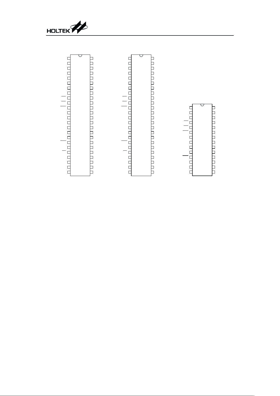
Pin Assignment
HT1621
3 April 21, 2000
SEG7
SEG6
SEG5
SEG4
SEG3
SEG2
SEG1
SEG0
CS
RD
WR
DATA
VSS
OSCO
NC
OSCI
VDD /VLCD
IR Q
BZ
BZ
COM 0
COM 1
COM 2
COM 3
SEG8
SEG9
SEG10
SEG11
SEG12
SEG13
SEG14
SEG15
SEG16
SEG17
SEG18
SEG19
SEG20
SEG21
SEG22
SEG23
SEG24
SEG25
SEG26
SEG27
SEG28
SEG29
SEG30
SEG31
H T 1621
-
48 S S O P
SEG7
SEG6
SEG5
SEG4
SEG3
SEG2
SEG1
SEG0
CS
RD
WR
DATA
VSS
OSCO
OSCI
VLCD
VDD
IR Q
BZ
BZ
COM 0
COM 1
COM 2
COM 3
SEG8
SEG9
SEG10
SEG11
SEG12
SEG13
SEG14
SEG15
SEG16
SEG17
SEG18
SEG19
SEG20
SEG21
SEG22
SEG23
SEG24
SEG25
SEG26
SEG27
SEG28
SEG29
SEG30
SEG31
H T 1621B
-
4 8 S S O P /D IP
48
47
46
45
44
43
42
41
40
39
38
37
36
35
34
33
32
31
30
29
28
27
26
25
1
2
3
4
5
6
7
8
9
10
11
12
13
14
15
16
17
18
19
20
21
22
23
24
48
47
46
45
44
43
42
41
40
39
38
37
36
35
34
33
32
31
30
29
28
27
26
25
1
2
3
4
5
6
7
8
9
10
11
12
13
14
15
16
17
18
19
20
21
22
23
24
SEG5
SEG3
SEG1
CS
RD
WR
DATA
VSS
VLCD
VDD
IR Q
BZ
COM 0
COM 1
H T 1621D
-
28 S kinny
SEG7
SEG9
SEG11
SEG13
SEG15
SEG17
SEG19
SEG21
SEG23
SEG25
SEG27
SEG29
SEG31
COM 2
28
27
26
25
24
23
22
21
20
19
18
17
16
15
1
2
3
4
5
6
7
8
9
10
11
12
13
14
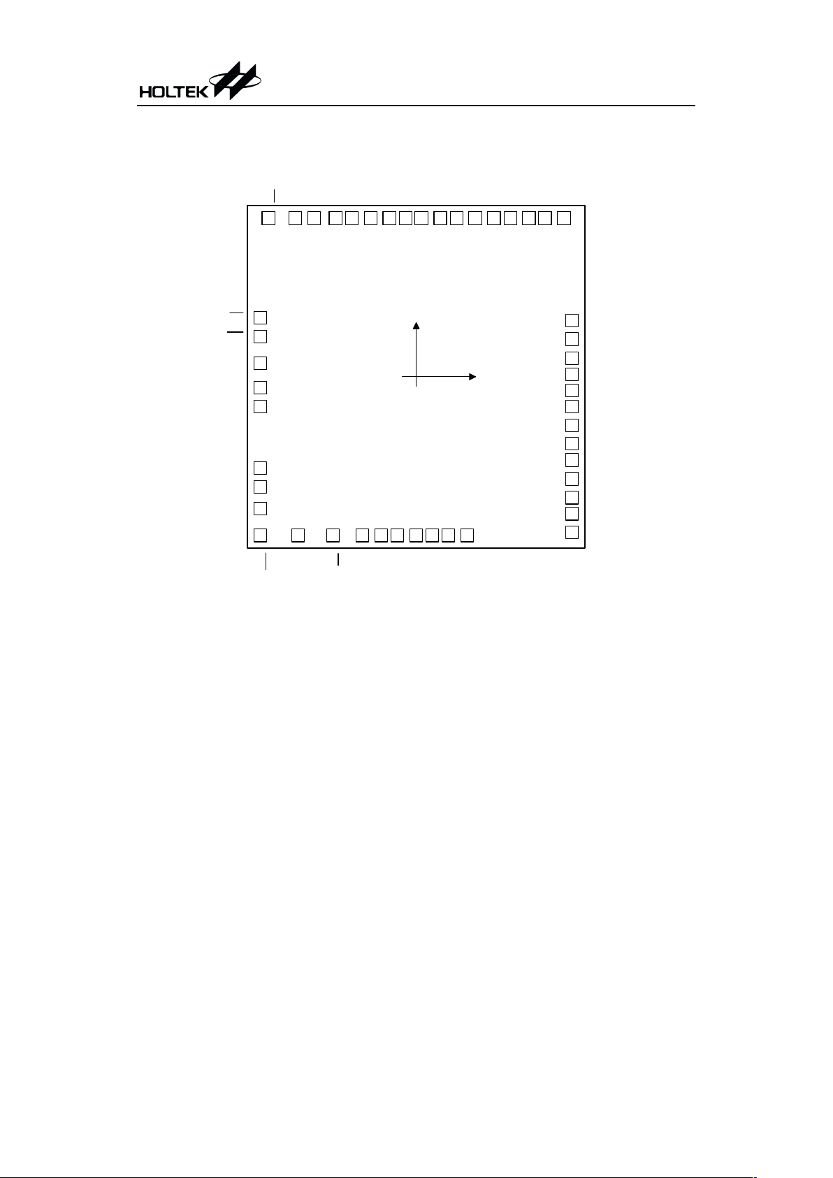
Pad Assignment
Chip size: 127 ´ 129 (mil)
2
* The IC substrate should be connected to VDD in the PCB layout artwork.
HT1621
4 April 21, 2000
IR Q
BZ
CS
1
2
3
4
5
6
7
8
9
10
11
12 13
14 15 16 17 18 19
20
21
22
23
24
25
26
27
28
29
30
31
32
3334353637383940
41
4243
44
45464748
(0 ,0 )
RD
WR
DATA
VSS
OSCO
OSCI
VLCD
VDD
BZ
COM 0
COM 1
COM 2
COM 3
SEG31
SEG30
SEG29
SEG28
SEG27
SEG26
SEG25
SEG24
SEG23
SEG22
SEG21
SEG20
SEG19
SEG18
SEG17
SEG16
SEG15
SEG14
SEG13
SEG12
SEG11
SEG10
SEG9
SEG8
SEG7
SEG6
SEG5
SEG4
SEG3
SEG2
SEG1
SEG0

Pad Coordinates Unit:mil
Pad No. X Y Pad No. X Y
1
-55.04
59.46 25 58.14
-25.29
2
-58.52
22.18 26 58.14
-18.66
3
-58.52
15.56 27 58.14
-11.94
4
-58.52
5.36 28 58.14
-5.31
5
-58.52 -4.51
29 58.14 1.32
6
-58.52 -11.14
30 58.14 7.95
7
-58.52 -34.76
31 58.14 14.58
8
-58.52 -41.90
32 58.14 21.21
9
-58.52 -49.13
33 55.55 59.46
10
-58.52 -59.08
34 48.92 59.46
11
-44.07 -59.08
35 42.29 59.46
12
-31.58 -59.08
36 35.66 59.46
13
-20.70 -59.08
37 29.03 59.46
14
-13.98 -59.08
38 22.40 59.46
15
-7.05 -59.08
39 15.77 59.46
16
-0.34 -59.08
40 9.14 59.46
17 6.33
-59.08
41 2.42 59.46
18 12.96
-59.08
42
-4.21
59.46
19 19.59
-59.08
43
-10.84
59.46
20 58.14
-58.44
44
-17.47
59.46
21 58.14
-51.81
45
-24.10
59.46
22 58.14
-45.18
46
-30.73
59.46
23 58.14
-38.55
47
-38.17
59.46
24 58.14
-31.92
48
-45.39
59.46
HT1621
5 April 21, 2000
Pad Description
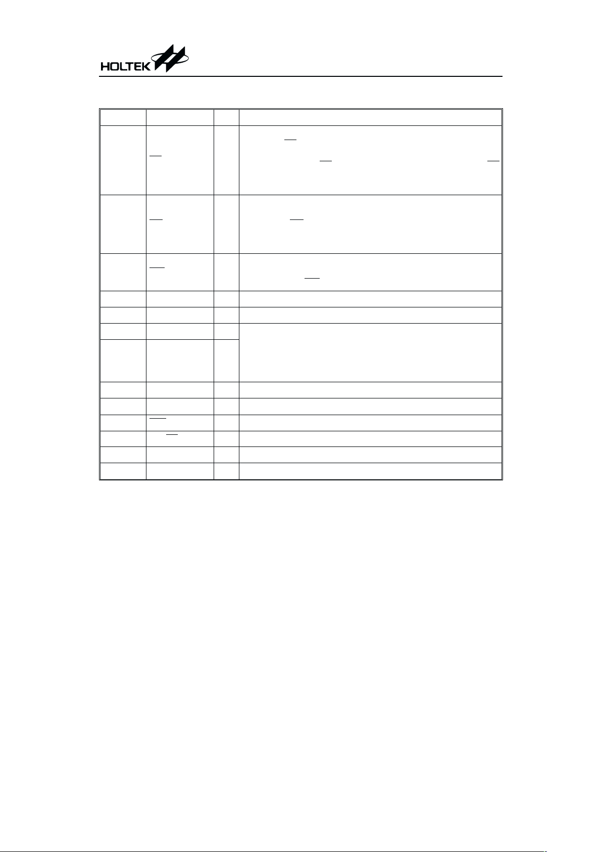
Pad No. Pad Name I/O Function
1CS
I
Chip selection input with pull-high resistor
When the CS
is logic high, the data and command read from or
written to the HT1621 are disabled. The serial interface circuit
is also reset. But if CS
is at logic low level and is input to the CS
pad, the data and command transmission between the host con
-
troller and the HT1621 are all enabled.
2RD
I
READ clock input with pull-high resistor
Data in the RAM of the HT1621 are clocked out on the falling
edge of the RD signal. The clocked out data will appear on the
DATA line. The host controller can use the next rising edge to
latch the clocked out data.
3WR
I
WRITE clock input with pull-high resistor
Data on the DATA line are latched into the HT1621 on the ris
-
ing edge of the WR
signal.
4 DATA I/O Serial data input/output with pull-high resistor
5 VSS
¾
Negative power supply, ground
7 OSCI I The OSCI and OSCO pads are connected to a 32.768kHz crystal
in order to generate a system clock. If the system clock comes
from an external clock source, the external clock source should
be connected to the OSCI pad. But if an on-chip RC oscillator is
selected instead, the OSCI and OSCO pads can be left open.
6 OSCO O
8 VLCD I LCD power input
9 VDD
¾
Positive power supply
10 IRQ
O Time base or WDT overflow flag, NMOS open drain output
11, 12 BZ, BZ
O 2kHz or 4kHz tone frequency output pair
13~16 COM0~COM3 O LCD common outputs
48~17 SEG0~SEG31 O LCD segment outputs
Absolute Maximum Ratings
Supply Voltage.................................-0.3V~5.5V
Storage Temperature....................-50
o
C~125oC
Input Voltage ....................V
SS
-0.3V~VDD+0.3V
Operating Temperature..................-25
o
C~75oC
Note: These are stress ratings only. Stresses exceeding the range specified under Absolute Maxi
-
mum Ratings may cause substantial damage to the device. Functional operation of this de
vice at other conditions beyond those listed in the specification is not implied and prolonged
exposure to extreme conditions may affect device reliability.
HT1621
6 April 21, 2000

D.C. Characteristics
Ta=25°C
Symbol Parameter
Test Conditions
Min. Typ. Max. Unit
V
DD
Conditions
V
DD
Operating Voltage
¾¾
2.4
¾
5.2 V
I
DD1
Operating Current
3V
No load/LCD ON
On-chip RC oscillator
¾
150 300
mA
5V
¾
300 600
mA
I
DD2
Operating Current
3V
No load/LCD ON
Crystal oscillator
¾
60 120
mA
5V
¾
120 240
mA
I
DD3
Operating Current
3V
No load/LCD ON
External clock source
¾
100 200
mA
5V
¾
200 400
mA
I
STB
Standby Current
3V
No load
Power down mode
¾
0.1 5
mA
5V
¾
0.3 10
mA
V
IL
Input Low Voltage
3V
DATA, WR,CS,RD
0
¾
0.6 V
5V 0
¾
1.0 V
V
IH
Input High Voltage
3V
DATA, WR,CS,RD
2.4
¾
3.0 V
5V 4.0
¾
5.0 V
I
OL1
DATA, BZ, BZ, IRQ
3V
V
OL
=0.3V
0.5 1.2
¾
mA
5V
V
OL
=0.5V
1.3 2.6
¾
mA
I
OH1
DATA, BZ, BZ
3V
V
OH
=2.7V
-0.4 -0.8 ¾
mA
5V
V
OH
=4.5V
-0.9 -1.8 ¾
mA
I
OL2
LCD Common Sink
Current
3V
V
OL
=0.3V
80 150
¾mA
5V
V
OL
=0.5V
150 250
¾mA
I
OH2
LCD Common Source
Current
3V
V
OH
=2.7V
-80 -120 ¾mA
5V
V
OH
=4.5V
-120 -200 ¾mA
I
OL3
LCD Segment Sink
Current
3V
V
OL
=0.3V
60 120
¾mA
5V
V
OL
=0.5V
120 200
¾mA
I
OH3
LCD Segment Source
Current
3V
V
OH
=2.7V
-40 -70 ¾mA
5V
V
OH
=4.5V
-70 -100 ¾mA
R
PH
Pull-high Resistor
3V
DATA, WR,CS,RD
40 80 150
kW
5V 30 60 100
kW
HT1621
7 April 21, 2000

A.C. Characteristics
Ta=25°C
Symbol Parameter
Test Conditions
Min. Typ. Max. Unit
V
DD
Conditions
f
SYS1
System Clock 3V On-chip RC oscillator
¾
256
¾
kHz
5V
¾
256
¾
kHz
f
SYS2
System Clock
3V
Crystal oscillator
¾
32.768
¾
kHz
5V
¾
32.768
¾
kHz
f
SYS3
System Clock
3V
External clock source
¾
256
¾
kHz
5V
¾
256
¾
kHz
f
LCD
LCD Clock
¾
On-chip RC oscillator
¾
f
SYS1
/1024
¾
Hz
¾
Crystal oscillator
¾
f
SYS2
/128
¾
Hz
¾
External clock source
¾
f
SYS3
/1024
¾
Hz
t
COM
LCD Common Period
¾
n: Number of COM
¾
n/f
LCD
¾
s
f
CLK1
Serial Data Clock (WR pin)
3V
Duty cycle 50%
¾¾
150 kHz
5V
¾¾
300 kHz
f
CLK2
Serial Data Clock (RD pin)
3V
Duty cycle 50%
¾¾
75 kHz
5V
¾¾
150 kHz
f
TONE
Tone Frequency
¾
On-chip RC oscillator
¾
2.0 or 4.0
¾
kHz
t
CS
Serial Interface Reset Pulse
Width (Figure 3)
¾
CS
¾
250
¾
ns
t
CLK
WR,RDInput Pulse Width
(Figure 1)
3V
Write mode 3.34
¾¾
ms
Read mode 6.67
¾¾
5V
Write mode 1.67
¾¾
ms
Read mode 3.34
¾¾
t
r,tf
Rise/Fall Time Serial Data
Clock Width (Figure 1)
3V
¾¾
120
¾
ns
5V
t
su
Setup Time for DATA to WR,
RD
Clock Width (Figure 2)
3V
¾¾
120
¾
ns
5V
t
h
Hold Time for DATA to WR,
RD
Clock Width (Figure 2)
3V
¾¾
120
¾
ns
5V
t
su1
Setup Time for CS to WR,RD
Clock Width (Figure 3)
3V
¾¾
100
¾
ns
5V
t
h1
Hold Time for CS to WR,RD
Clock Width (Figure 3)
3V
¾¾
100
¾
ns
5V
HT1621
8 April 21, 2000

HT1621
9 April 21, 2000
Functional Description
Display memory - RAM
The static display memory (RAM) is organized
into 32´4 bits and stores the displayed data.
The contents of the RAM are directly mapped to
the contents of the LCD driver. Data in the
RAM can be accessed by the READ, WRITE,
and READ-MODIFY-WRITE commands. The
following is a mapping from the RAM to the
LCD pattern:
System oscillator
The HT1621 system clock is used to generate
the time base/Watchdog Timer (WDT) clock fre
-
quency, LCD driving clock, and tone frequency.
The source of the clock may be from an on-chip
RC oscillator (256kHz), a crystal oscillator
(32.768kHz), or an external 256kHz clock by
the S/W setting. The configuration of the system oscillator is as shown. After the SYS DIS
command is executed, the system clock will
stop and the LCD bias generator will turn off.
That command is, however, available only for
the on-chip RC oscillator or for the crystal oscillator. Once the system clock stops, the LCD display will become blank, and the time base/WDT
lose its function as well.
The LCD OFF command is used to turn the
LCD bias generator off. After the LCD bias gen
-
erator switches off by issuing the LCD OFF
command, using the SYS DIS command re
-
duces power consumption, serving as a system
power down command. But if the external clock
source is chosen as the system clock, using the
SYS DIS command can neither turn the oscilla
-
tor off nor carry out the power down mode. The
crystal oscillator option can be applied to con
-
nect an external frequency source of 32kHz to
the OSCI pin. In this case, the system fails to
SEG0
SEG1
SEG2
SEG3
SEG31
COM 0COM 1COM 2COM 3
D 3 D 2 D 1 D 0
Data
Addr
31
0
1
2
3
Address 6 bits
(A 5 , A 4 , ..., A 0 )
Data 4 bits
(D3, D 2, D 1, D0)
RAM mapping
90%
50%
10%
GN
D
W
R, RD
Clock
t
f
t
r
t
CLK
t
CLK
V
DD
Figure 1
50%
VALID DATA
50%
DB
W R , R D
Clock
GND
t
su
t
h
V
DD
V
DD
GND
Figure 2
CS
GND
50%
50%
FIRST
Clock
LAST
Clock
GND
WR, RD
Clock
t
su1
t
h1
t
CS
V
DD
V
DD
Figure 3

HT1621
10 April 21, 2000
enter the power down mode, similar to the case
in the external 256kHz clock source operation.
At the initial system power on, the HT1621 is at
the SYS DIS state.
Time base and Watchdog Timer (WDT)
The time base generator is comprised by an
8-stage count-up ripple counter and is designed
to generate an accurate time base. The watch
dog timer (WDT), on the other hand, is com
posed of an 8-stage time base generator along
with a 2-stage count-up counter, and is de
signed to break the host controller or other sub
systems from abnormal states such as
unknown or unwanted jump, execution errors,
etc. The WDT time-out will result in the setting
of an internal WDT time-out flag. The outputs
of the time base generator and of the WDT
time-out flag can be connected to the IRQ
out
put by a command option. There are totally
eight frequency sources available for the time
base generator and the WDT clock. The fre
quency is calculated by the following equation.
f
WDT
=
32kHz
2
n
where the value of n ranges from 0 to 7 by com
mand options. The 32kHz in the above equation
indicates that the source of the system fre
quency is derived from a crystal oscillator of
32.768kHz, an on-chip oscillator (256kHz), or
an external frequency of 256kHz.
If an on-chip oscillator (256kHz) or an external
256kHz frequency is chosen as the source of the
system frequency, the frequency source is by de
fault prescaled to 32kHz by a 3-stage prescaler.
Employing both the time base generator and
the WDT related commands, one should be
careful since the time base generator and WDT
share the same 8-stage counter. For example,
invoking the WDT DIS command disables the
time base generator whereas executing the
WDT EN command not only enables the time
base generator but activates the WDT time-out
flag output (connect the WDT time-out flag to
the IRQ
pin). After the TIMER EN command is
transferred, the WDT is disconnected from the
IRQ
pin, and the output of the time base generator
is connected to the IRQ
pin. The WDT can be
cleared by executing the CLR WDT command,
and the contents of the time base generator is
cleared by executing the CLR WDT or the CLR
1/8
OSCI
OSCO
C rystal O scillator
32768H z
E x te rn a l C lo c k S o u rc e
256kHz
O n - c h ip R C O s c illa t o r
256kHz
S ystem
Clock
System oscillator configuration
TIM ER E N/DIS
W D T E N /D IS
V
DD
IR Q
IR Q E N /D IS
D
CK
Q
R
CLR W DT
S ystem C lock
f=32kH z
/256
/4
WDT
Tim er/W D T
C lock S ources
/2
n
n=0~7
Timer and WDT configurations

HT1621
11 April 21, 2000
TIMER command. The CLR WDT or the CLR
TIMER command should be executed prior to
the WDT EN or the TIMER EN command re
-
spectively. Before executing the IRQ
EN com
mand the CLR WDT or CLR TIMER command
should be executed first. The CLR TIMER com
mand has to be executed before switching from
the WDT mode to the time base mode. Once the
WDT time-out occurs, the IRQ
pin will stay at a
logic low level until the CLR WDT or the IRQ
DIS command is issued. After the IRQ output is
disabled the IRQ
pin will remain at the floating
state. The IRQ
output can be enabled or dis
-
abled by executing the IRQ
EN or the IRQ DIS
command, respectively. The IRQ
EN makes the
output of the time base generator or of the WDT
time-out flag appear on the IRQ
pin. The configuration of the time base generator along with
the WDT are as shown. In the case of on-chip
RC oscillator or crystal oscillator, the power
down mode can reduce power consumption
since the oscillator can be turned on or off by
the corresponding system commands. At the
power down mode the time base/WDT loses all
its functions.
On the other hand, if an external clock is se
lected as the source of system frequency the
SYS DIS command turns out invalid and the
power down mode fails to be carried out. That
is, after the external clock source is selected,
the HT1621 will continue working until system
power fails or the external clock source is re
moved. After the system power on, the IRQ
will
be disabled.
Tone output
A simple tone generator is implemented in the
HT1621. The tone generator can output a pair
of differential driving signals on the BZ and BZ,
which are used to generate a single tone. By ex
ecuting the TONE4K and TONE2K commands
there are two tone frequency outputs
selectable. The TONE4K and TONE2K com
mands set the tone frequency to 4kHz and
2kHz, respectively. The tone output can be
turned on or off by invoking the TONE ON or
the TONE OFF command. The tone outputs,
namely BZ and BZ
, are a pair of differential
driving outputs used to drive a piezo buzzer.
Once the system is disabled or the tone output
is inhibited, the BZ and the BZ
outputs will re-
main at low level.
LCD driver
The HT1621 is a 128 (32´4) pattern LCD driver.
It can be configured as 1/2 or 1/3 bias and 2 or 3
or 4 commons of LCD driver by the S/W configuration. This feature makes the HT1621 suitable
for multiply LCD applications. The LCD driving
clock is derived from the system clock. The value
of the driving clock is always 256Hz even when it
is at a 32.768kHz crystal oscillator frequency, an
on-chip RC oscillator frequency, or an external
frequency. The LCD corresponding commands
are summarized in the table.
The bold form of100,namely 100, indicates
the command mode ID. If successive commands
have been issued, the command mode ID except
for the first command, will be omitted. The LCD
Name Command Code Function
LCD OFF
10000000010X
Turn off LCD outputs
LCD ON
10000000011X
Turn on LCD outputs
BIAS & COM
1000010abXcX
c=0: 1/2 bias option
c=1: 1/3 bias option
ab=00: 2 commons option
ab=01: 3 commons option
ab=10: 4 commons option

HT1621
12 April 21, 2000
OFF command turns the LCD display off by dis
abling the LCD bias generator. The LCD ON
command, on the other hand, turns the LCD
display on by enabling the LCD bias generator.
The BIAS and COM are the LCD panel related
commands. Using the LCD related commands,
the HT1621 can be compatible with most types
of LCD panels.
Command format
The HT1621 can be configured by the S/W set
ting. There are two mode commands to configure
the HT1621 resources and to transfer the LCD
display data. The configuration mode of the
HT1621 is called command mode, and its com
mand mode ID is 100. The command mode con
sists of a system configuration command, a
system frequency selection command, a LCD con
figuration command, a tone frequency selection
command, a timer/WDT setting command, and
an operating command. The data mode, on the
other hand, includes READ, WRITE, and
READ-MODIFY-WRITE operations. The follow
ing are the data mode IDs and the command
mode ID:
Operation Mode ID
READ Data 1 1 0
WRITE Data 1 0 1
READ-MODIFY-WRITE Data 1 0 1
COMMAND Command 1 0 0
The mode command should be issued before the
data or command is transferred. If successive
commands have been issued, the command
mode ID, namely 100, can be omitted. While
the system is operating in the non-successive
command or the non-successive address data
mode, the CS
pin should be set to "1" and the
previous operation mode will be reset also.
Once the CS
pin returns to "0" a new operation
mode ID should be issued first.
Interfacing
Only four lines are required to interface with
the HT1621. The CS
line is used to initialize the
serial interface circuit and to terminate the com
munication between the host controller and the
HT1621. If the CS
pin is set to 1, the data and
command issued between the host controller and
the HT1621 are first disabled and then initial
ized. Before issuing a mode command or mode
switching, a high level pulse is required to initial
ize the serial interface of the HT1621. The DATA
line is the serial data input/output line. Data to
be read or written or commands to be written
have to be passed through the DATA line. The RD
line is the READ clock input. Data in the RAM
are clocked out on the falling edge of the RD
sig
nal, and the clocked out data will then appear on
the DATA line. It is recommended that the host
controller read in correct data during the interval
between the rising edge and the next falling edge
of the RD
signal. The WR line is the WRITE clock
input. The data, address, and command on the
DATA line are all clocked into the HT1621 on the
rising edge of the WR
signal. There is an optional
IRQ
line to be used as an interface between the
host controller and the HT1621. The IRQ
pin can
be selected as a timer output or a WDT overflow
flag output by the S/W setting. The host controller can perform the time base or the WDT function by being connected with the IRQ
pin of the
HT1621.

Timing Diagrams
READ mode (command code:110)
READ mode (successive address reading)
HT1621
13 April 21, 2000
RD
DATA
WR
1
1
0A5A4A3 A2
A1A0D0D1
D2
D3
M em ory Address 1 (M A1) D ata (M A 2)
1
1
0A5A4A3 A2
A1A0D0D1
D2
D3
D ata (M A 1) M em ory Address 2 (M A2)
CS
RD
DATA
CS
WR
1
1
0A5A4A3 A2
A1A0D0D1
D2
D3
M e m o ry A d d re s s ( M A ) D a ta (M A )
D0D1
D2
D3
D0D1
D2
D3
D0D1
D2
D3
D0
D a ta (M A + 1 ) D a ta (M A + 2 ) D a ta (M A + 3 )

WRITE mode (command code:101)
WRITE mode (successive address writing)
HT1621
14 April 21, 2000
DATA
CS
WR
1
0
1A5A4A3 A2
A1A0D0D1
D2
D3
M em ory Address 1 (M A1)D ata (M A 1)
1
0
1A5A4A3 A2
A1A0D0D1
D2
D3
M em ory Address 2 (M A2)D ata (M A 2)
DATA
CS
WR
1
0
1A5A4A3 A2
A1A0D0D1
D2
D3
M e m o ry A d d re s s ( M A ) D a ta (M A )
D0D1
D2
D3
D0D1
D2
D3
D0D1
D2
D3
D0
D a ta (M A + 1 ) D a ta (M A + 2 ) D a ta (M A + 3 )

READ-MODIFY-WRITE mode (command code:101)
READ-MODIFY-WRITE mode (successive address accessing)
HT1621
15 April 21, 2000
DATA
CS
WR
1
0
1A5A4A3 A2
A1A0D0D1
D2
D3
M em ory Address 1 (M A 1)D ata (M A 1)
A5A4A3 A2
A1A0D0D1
D2
D3
M em ory Address 2 (M A 2)D ata (M A 2)
1
0
1
RD
D0D1
D2
D3
D a ta ( M A 1 )
DATA
CS
WR
1
0
1A5A4A3 A2
A1A0D0D1
D2
D3
M e m o r y A d d r e s s (M A ) D a ta ( M A )
D0D1
D2
D3
D0D1
D2
D3
D0D1
D2
D3
D0
D a ta ( M A ) D a ta (M A + 1 ) D a ta (M A + 1 )
RD
D1
D2
D3
D0
D a ta ( M A + 2 )

Command mode (command code:100)
Mode (data and command mode)
Note: It is recommended that the host controller should read in the data from the DATA line
between the rising edge of the RD
line and the falling edge of the next RD line.
HT1621
16 April 21, 2000
DATA
CS
WR
1
0
0C8C7C6 C5
C4C3C2C1
C0
C om m and 1
C8C7C6 C5
C4C3C2C1
C0
C om m and iC om m and... C om m and
or
D a ta M o d e
RD
DATA
CS
WR
Address & D ata
C om m and
or
D a ta M o d e
Address and D ata
C om m and
or
D a ta M o d e
Address and D ata
C om m and
or
D a ta M o d e

Application Circuits
Host controller with an HT1621 display system
Note:
The connection of IRQ
and RD pin can be selected depending on the requirement of the mC.
The voltage applied to V
LCD
pin must be lower than VDD.
Adjust VR to fit LCD display, at V
DD
=5V, V
LCD
=4V, VR=15kW±20%.
Adjust R (external pull-high resistance) to fit user s time base clock.
HT1621
17 April 21, 2000
IR Q
DATA
*
O n-chip O S C
OSCI
OSCO
C lock O u t
E x te rn a l C o lc k 1
E x te rn a l C o lc k 2
CS
RD
WR
m
C
C rystal
32768H z
H T 1621B
LCD P anel
BZ
BZ
CO M 0 ~ COM 3 SEG 0~SEG31
Piezo
1/2 or 1/3 B ias; 1/2, 1/3 or 1/4 Duty
R
*
VR
*
VDD
VLCD

Command Summary
HT1621
18 April 21, 2000
Name ID Command Code D/C Function Def.
READ
110
A5A4A3A2A1A0D0D1D2D3 D Read data from the RAM
WRITE
101
A5A4A3A2A1A0D0D1D2D3 D Write data to the RAM
READMODIFYWRITE
101
A5A4A3A2A1A0D0D1D2D3 D READ and WRITE to the RAM
SYS DIS
100
0000-0000-X C
Turn off both system oscillator
and LCD bias generator
Yes
SYS EN
100
0000-0001-X C Turn on system oscillator
LCD OFF
100
0000-0010-X C Turn off LCD bias generator Yes
LCD ON
100
0000-0011-X C Turn on LCD bias generator
TIMER DIS
100
0000-0100-X C Disable time base output
WDT DIS
100
0000-0101-X C
Disable WDT time-out flag
output
TIMER EN
100
0000-0110-X C Enable time base output
WDT EN
100
0000-0111-X C
Enable WDT time-out flag
output
TONE OFF
100
0000-1000-X C Turn off tone outputs Yes
TONE ON
100
0000-1001-X C Turn on tone outputs
CLR TIMER
100
0000-11XX-X C
Clear the contents of time base
generator
CLR WDT
100
0000-111X-X C Clear the contents of WDT stage
XTAL 32K
100
0001-01XX-X C
System clock source, crystal
oscillator
RC 256K
100
0001-10XX-X C
System clock source, on-chip RC
oscillator
Yes
EXT 256K
100
0001-11XX-X C
System clock source, external
clock source
BIAS 1/2
100
0010-abX0-X C
LCD 1/2 bias option
ab=00: 2 commons option
ab=01: 3 commons option
ab=10: 4 commons option
BIAS 1/3
100
0010-abX1-X C
LCD 1/3 bias option
ab=00: 2 commons option
ab=01: 3 commons option
ab=10: 4 commons option
TONE 4K
100
010X-XXXX-X C Tone frequency, 4kHz
TONE 2K
100
011X-XXXX-X C Tone frequency, 2kHz
IRQ
DIS
100
100X-0XXX-X C Disable IRQ output Yes

HT1621
19 April 21, 2000
Name ID Command Code D/C Function Def.
IRQ
EN
100
100X-1XXX-X C Enable IRQ output
F1
100
101X-X000-X C
Time base/WDT clock
output:1Hz
The WDT time-out flag after: 4s
F2
100
101X-X001-X C
Time base/WDT clock
output:2Hz
The WDT time-out flag after: 2s
F4
100
101X-X010-X C
Time base/WDT clock
output:4Hz
The WDT time-out flag after: 1s
F8
100
101X-X011-X C
Time base/WDT clock
output:8Hz
The WDT time-out flag after: 1/2 s
F16
100
101X-X100-X C
Time base/WDT clock
output:16Hz
The WDT time-out flag after: 1/4 s
F32
100
101X-X101-X C
Time base/WDT clock
output:32Hz
The WDT time-out flag after: 1/8 s
F64
100
101X-X110-X C
Time base/WDT clock
output:64Hz
The WDT time-out flag after: 1/16 s
F128
100
101X-X111-X C
Time base/WDT clock
output:128Hz
The WDT time-out flag after: 1/32 s
Yes
TEST
100
1110-0000-X C Test mode, user don't use.
NORMAL
100
1110-0011-X C Normal mode Yes
Note: X : Don,t care
A5~A0 : RAM addresses
D3~D0 : RAM data
D/C : Data/command mode
Def. : Power on reset default
All the bold forms, namely 110, 101, and 100, are mode commands. Of these, 100indicates
the command mode ID. If successive commands have been issued, the command mode ID ex
cept for the first command will be omitted. The source of the tone frequency and of the time
base/WDT clock frequency can be derived from an on-chip 256kHz RC oscillator, a 32.768kHz
crystal oscillator, or an external 256kHz clock. Calculation of the frequency is based on the
system frequency sources as stated above. It is recommended that the host controller should
initialize the HT1621 after power on reset, for power on reset may fail, which in turn leads to
the malfunctioning of the HT1621.

HT1621
20 April 21, 2000
Copyright Ó 2000 by HOLTEK SEMICONDUCTOR INC.
The information appearing in this Data Sheet is believed to be accurate at the time of publication. However, Holtek
assumes no responsibility arising from the use of the specifications described. The applications mentioned herein are
used solely for the purpose of illustration and Holtek makes no warranty or representation that such applications
will be suitable without further modification, nor recommends the use of its products for application that may pres
ent a risk to human life due to malfunction or otherwise. Holtek reserves the right to alter its products without prior
notification. For the most up-to-date information, please visit our web site at http://www.holtek.com.tw.
Holtek Semiconductor Inc. (Headquarters)
No.3 Creation Rd. II, Science-based Industrial Park, Hsinchu, Taiwan, R.O.C.
Tel: 886-3-563-1999
Fax: 886-3-563-1189
Holtek Semiconductor Inc. (Taipei Office)
5F, No.576, Sec.7 Chung Hsiao E. Rd., Taipei, Taiwan, R.O.C.
Tel: 886-2-2782-9635
Fax: 886-2-2782-9636
Fax: 886-2-2782-7128 (International sales hotline)
Holtek Semiconductor (Hong Kong) Ltd.
RM.711, Tower 2, Cheung Sha Wan Plaza, 833 Cheung Sha Wan Rd., Kowloon, Hong Kong
Tel: 852-2-745-8288
Fax: 852-2-742-8657
 Loading...