

Page 1
1/4 to 1/12 Duty VFD Controller
Features
·
Logic voltage: 3.0V~5.5V
·
High-voltage output: VDD-35V max.
·
Multiple display
(16-segment & 12-digit to 24-segment & 4-digit)
·
16´2 matrix key scanning
·
8 steps dimmer circuit
Applications
·
Consumer products panel function control
·
Industrial measuring instrument panel function control
General Description
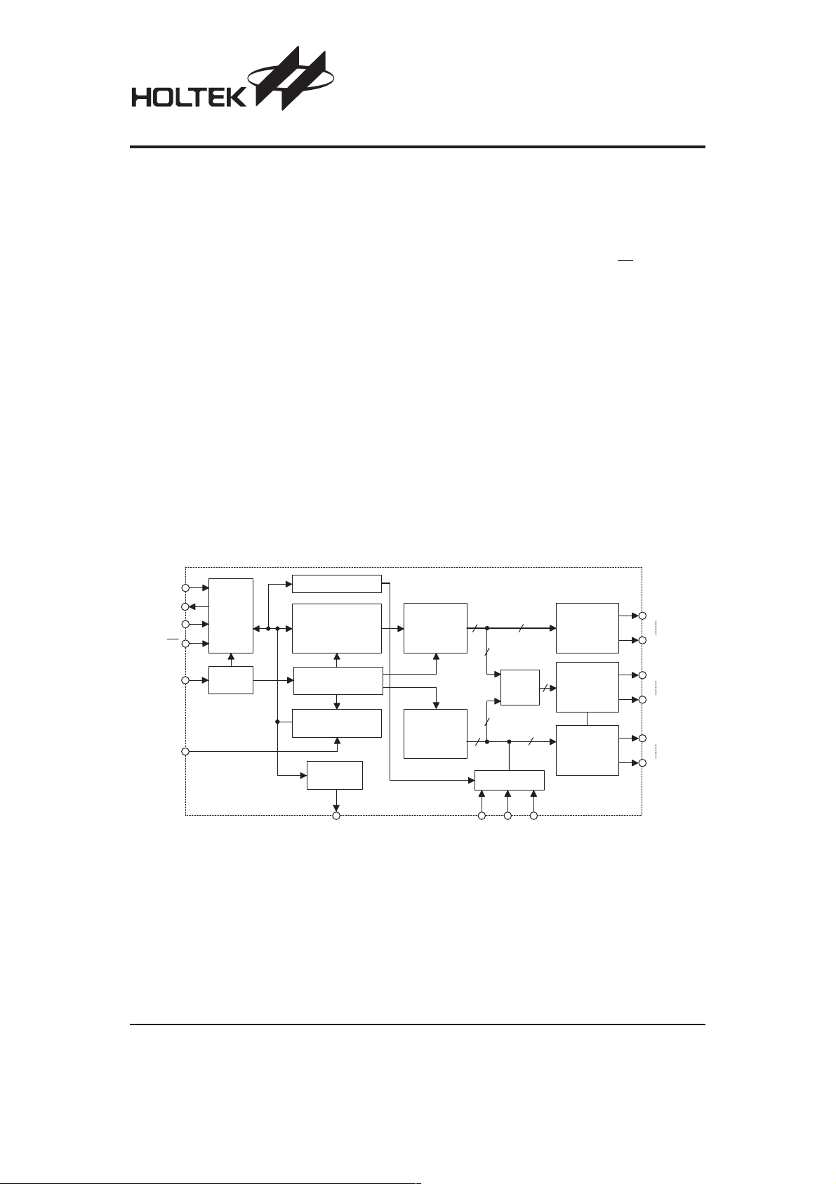
HT16515 is a VFD (Vacuum Fluorescent Display) con
troller/driver that is driven on a 1/4 to 1/12 duty factor. It
consists of 16 segment output lines, 4 grid output lines,
8 segment/grid output drive lines, 4 LED output ports, a
control circuit, a displaymemory, and a key scan circuit.
HT16515
·
4 LED output ports
·
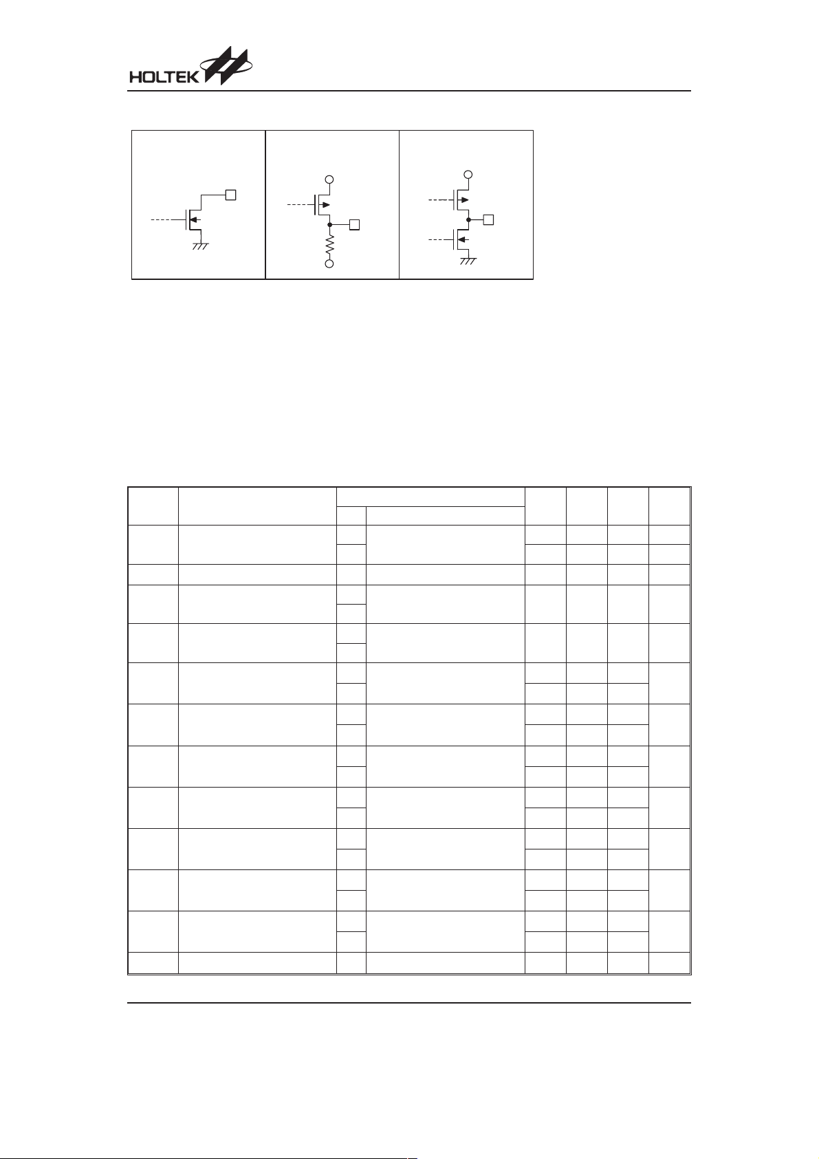
No external resistors necessary for driver output
(provides PMOS open-drain and pull-low resistor
output)
·
Serial interface with MCU (CLK, CS, DI, DO)
·
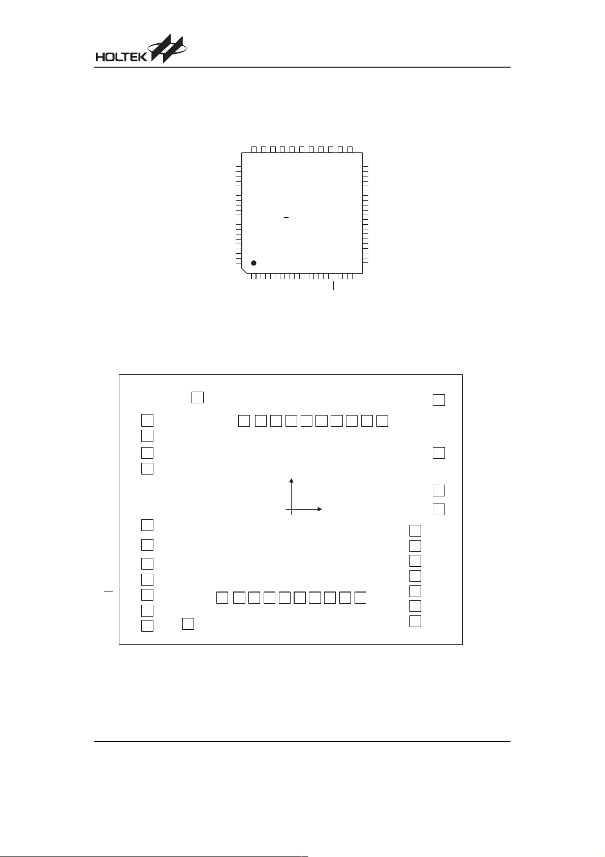
44-pin QFP package
·
Other similarapplications for panel function control
Serial data inputs to the HT16515 through a three-line
serial interface. This VFD controller/driver is an ideal
MCU peripheral device.
Block Diagram
D I
D O
C L K
C S
O S C
K e y 0 ~ K e y 1
S e r i a l I / F
O S C
C o m m a n d D e c o d e r
D i s p l a y R A M
2 4 - B i t
1 2 W o r d s
´
T i m i n g G e n e r a t o r
K e y S c a n
K e y D a t a M e m o r y
( 2
1 6 )
´
4 - B i t L a t c h
L E D 0 ~ L E D 3
2 4 - B i t
O u t p u t L a t c h
1 2 - B i t
S h i f t R e g i s t e r
2 4 1 6
8
D a t a
S e l e c t o r
8
1 2
D i m m i n g C i r c u i t
V D D V S S V E E
S e g m e n t
D r i v e r
8
M u l t i p l e x e d
D r i v e r
4
G r i d
D r i v e r
S e g 1 / K S 1
S e g 1 6 / K S 1 6
S e g 1 7 / G r i d 1 2
S e g 2 4 / G r i d 5
G r i d 1
G r i d 4
Rev. 1.30 1 November 21, 2006
Page 2
Pin Assignment
S e g 2 0 / G r i d 9
S e g 2 1 / G r i d 8
S e g 2 2 / G r i d 7
S e g 2 3 / G r i d 6
S e g 2 4 / G r i d 5
G r i d 4
G r i d 3
G r i d 2
G r i d 1
V D D
V S S
HT16515
S e g 1 0 / K S 1 0
S e g 1 1 / K S 1 1
S e g 1 2 / K S 1 2
S e g 1 3 / K S 1 3
S e g 1 4 / K S 1 4
S e g 1 5 / K S 1 5
S e g 1 6 / K S 1 6
V E E
S e g 1 7 / G r i d 1 2
S e g 1 8 / G r i d 1 1
S e g 1 9 / G r i d 1 0
3 4
3 5
3 6
3 7
3 8
3 9
4 0
4 1
4 2
4 3
4 4
1 2
L E D 0
L E D 1
3 4 5
L E D 2
L E D 3
0 6 $ # #
" " 3 . 2
6 7 8 9 1 0 1 1
O S C
D O
D I
2 32 42 52 62 72 82 93 03 13 23 3
2 2
S e g 9 / K S 9
2 1
S e g 8 / K S 8
2 0
S e g 7 / K S 7
1 9
S e g 6 / K S 6
1 8
S e g 5 / K S 5
1 7
S e g 4 / K S 4
1 6
S e g 3 / K S 3
1 5
S e g 2 / K S 2
1 4
S e g 1 / K S 1
1 3
V D D
1 2
V S S
C L K
C S
K E Y 0
K E Y 1
Pad Assignment
L E D 0
L E D 1
L E D 2
L E D 3
O S C
D O
D I
C L K
C S
K E Y 0
K E Y 1
1
2
3
4
5
6
7
8
9
1 0
1 1
S e g 2 0 / G r i d 9
S e g 2 1 / G r i d 8
S e g 2 2 / G r i d 7
S e g 2 3 / G r i d 6
S e g 2 4 / G r i d 5
G r i d 4
G r i d 3
G r i d 2
G r i d 1
V S S
4 4
1 2
V D D
4 3
4 2
1 3 1 4 1 5 1 6
3 3
3 9
4 0
( 0 , 0 )
1 8
3 8
3 7
2 0
2 1
1 9
4 1
1 7
3 4
3 5
3 6
3 2
3 1
3 0
2 9
2 8
2 7
2 6
2 2
2 5
2 4
2 3
S e g 1 9 / G r i d 1 0
S e g 1 8 / G r i d 1 1
S e g 1 7 / G r i d 1 2
V E E
S e g 1 6 / K S 1 6
S e g 1 5 / K S 1 5
S e g 1 4 / K S 1 4
S e g 1 3 / K S 1 3
S e g 1 2 / K S 1 2
S e g 1 1 / K S 1 1
S e g 1 0 / K S 1 0
V D D
V S S
S e g 9 / K S 9
S e g 8 / K S 8
S e g 7 / K S 7
S e g 6 / K S 6
S e g 5 / K S 5
S e g 4 / K S 4
S e g 3 / K S 3
S e g 2 / K S 2
S e g 1 / K S 1
Chip Size:
* The IC substrate should be connected to VSS in the PCB layout artwork.
Rev. 1.30 2 November 21, 2006
Page 3
HT16515
Pad Coordinates
Pad No. X Y Pad No. X Y
1
2
3
4
5
6
7
8
9
10
11
12
13
14
15
16
17
18 61.35
19 162.75
20 264.15
21 365.55
22 466.95
-962.50
-962.50
-962.50
-962.50
-962.50 -107.20
-962.50 -235.60
-962.50 -366.00
-962.50 -471.00
-962.50 -576.00
-962.50 -681.00
-962.50 -786.00
-689.60 -772.45
-460.45 -595.30
-344.25 -595.30
-242.85 -595.30
-141.45 -595.30
-40.05 -595.30
600.00
495.00 24 834.10
380.20 25 834.10
275.20 26 834.10
-595.30
-595.30
-595.30
-595.30
-595.30
23
27 834.10
28 834.10
29 834.10
30 987.30 0.50
31 987.30 130.50
32 987.30 382.05
33 987.30 734.05
34 610.30 594.40
35 508.90 594.40
36 407.50 594.40
37 306.10 594.40
38 204.70 594.40
39 103.30 594.40
40 1.90 594.40
41
42
43
44
834.10
-99.50
-200.90
-317.10
-624.50
Unit: mm
-754.00
-652.60
-551.20
-449.80
-348.40
-247.00
-145.60
594.40
594.40
594.40
756.80
Pin Description
Pin No. Pin Name I/O Description
1~4 LED3~LED0 O
5 OSC I Connected to an external resistor or an RC oscillator circuit.
6DO O
7DI I
8 CLK I
9CS
10, 11 Key0, Key1 I Key-in data input to these pins are latched at the end of the display cycle.
12, 44 VSS
13, 43 VDD
14~29 Seg1/KS1~Seg16/KS16 O
30 VEE
31~38
39~42 Grid4~Grid1 O
Seg17/Grid12~
Seg24/Grid5
LED driver output ports. This is a CMOS output pin and maximum driving
current up to +20mA.
Data output pin, output serial data at falling edge of shift clock, starting from
the lower bit. This is N-ch open-drain output pin.
Data input pin, input serial data at rising edge of shift clock, starting from the
lower bit.
Clock input pin. Reads serial data at the rising edge, and outputs data at the
falling edge.
Initializes serial interface at the rising or falling edge of the HT16515. Then
it waits to receive a command. Data input after CS
I
current processing is stopped, and the serial interface is initialized. While
CS
is high, CLK is ignored.
Negative power supply, ground
¾
Positive power supply
¾
High voltage output, segment output pins, dual function as key source. This
is PMOS open-drain and pull-low resistor output.
VFD power supply
¾
High voltage output, these pins are selectable for segment or grid output.
O
This is PMOS open-drain and pull-low resistor output.
High voltage output, grids output pin. This is PMOS open-drain and pull-low
resistor output.
has fallen is processed,
Rev. 1.30 3 November 21, 2006
Page 4
Approximate Internal Connections
HT16515
N M O S O U T
P M O S O U T C M O S O U T
V
V
D D
V
E E
D D
Absolute Maximum Ratings
Supply Voltage...........................VSS-0.3V to VSS+6.0V
Input Voltage..............................V
-0.3V to VDD+0.3V
SS
Note: These are stress ratings only. Stresses exceeding the range specified under ²Absolute Maximum Ratings² may
cause substantial damage to the device. Functional operation of this device at other conditions beyond those
listed in the specification is not implied and prolonged exposure to extreme conditions may affect device reliabil
ity.
D.C. Characteristics
Symbol Parameter
V
V
f
OSC
R
I
DD
I
OL
I
OL1
I
OH1
I
OH21
I
OH22
I
OL3
V
DD
EE
PL
IH
Logic Supply Voltage
VFD Supply Voltage
Oscillation Frequency
Output Pull-low Resistor
Operating Current
Driver Leakage Current
LED Sink Current
LED Source Current
Segment 1~16 Source Current
Segment 17~24, Grid 1~4
Source Current
DO Sink Current
²H² Input Voltage ¾¾
V
DD
3.3V
5V 4.5 5 5.5 V
¾¾
3.3V
R
OSC
5V
3.3V
Driver output 40 65 120
5V
3.3V
No load, VFD display off,
data output =00H
5V
3.3V
V
O=VDD
5V
3.3V
V
OL
5V 20
3.3V
V
OH
5V
3.3V
V
OH=VDD
5V
3.3V
V
OH=VDD
5V
3.3V
V
OL
5V 4
Operating Temperature...........................-25°Cto75°C
Storage Temperature ............................-50°Cto125°C
Ta=25°C, VEE=VDD-35V
Test Conditions
Conditions
¾
=82kW
Min. Typ. Max. Unit
3 3.3 3.6 V
0
¾ V
350 500 650 kHz
¾¾
¾¾
-35V, VFD driver off
¾¾-5
¾¾-10
10
=1V, LED0~LED3
¾¾
¾¾
=0.9VDD, LED0~LED3
¾¾-1.5
¾¾-3
-2V
¾¾-1.5
¾¾-3
-2V
¾¾-7.5
¾¾-15
2
=0.4V
¾¾
¾¾
0.7V
DD
¾
DD
V
-35
kW
3
mA
5
mA
mA
mA
mA
mA
mA
V
DD
V
-
Rev. 1.30 4 November 21, 2006
Page 5
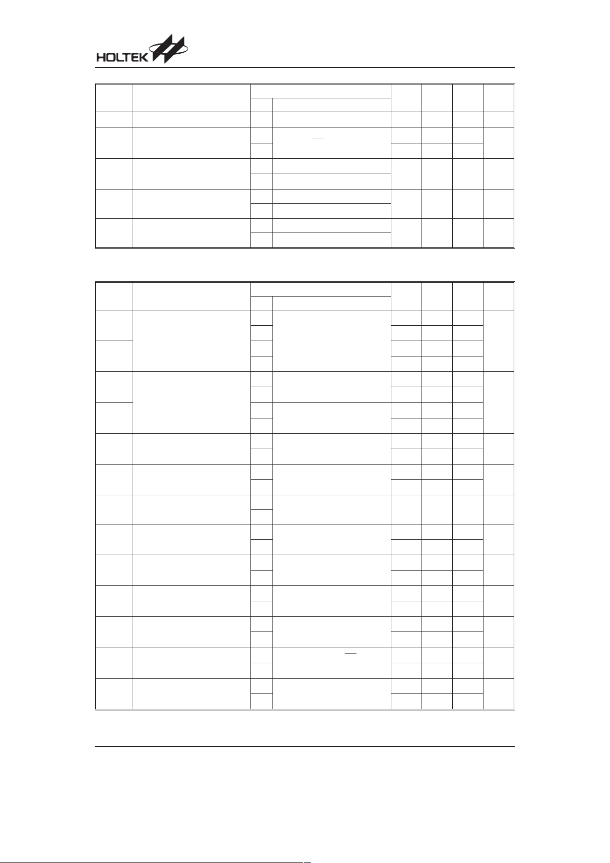
HT16515
Symbol Parameter
V
IL
V
H
V
OH1
V
OL1
V
OL2
²L² Input Voltage ¾¾
Hysteresis Voltage
High-level Output Voltage
Low-level Output Voltage
Low-level Output Voltage
A.C. Characteristics
Symbol Parameter
t
PHL
Logic Supply Voltage
t
PLH
t
r1
Rise Time
t
r2
t
t
C
t
t
t
t
t
t
f
max
i
CW
SW
SU
h
CS
W
Fall Time
Maximum Clock Frequency
Input Capacitance
Clock Pulse Width
Strobe Pulse Width
Data Setup Time
Data Hold Time
Clock-Strobe Time
Wait Time
Test Conditions
V
DD
3.3V
CLK, D
5V
3.3V
LED0~LED3, I
5V
LED0~LED3, I
Conditions
,CS
IN
3.3V LED0~LED3, I
5V LED0~LED3, I
3.3V DO, I
5V DO, I
OL2
OL2
=2mA
=4mA
Test Conditions
V
DD
Conditions
OH1
OH1
OL1
OL1
=-1.5mA
=-3mA
=10mA
=20mA
Min. Typ. Max. Unit
0.9V
Min. Typ. Max. Unit
3.3V
5V
CLK®DO
C
=15pF, RL=10kW
L
3.3V
5V
3.3V
C
=300pF, S1~S16
L
5V
3.3V
3.3V
3.3V
3.3V
3.3V
3.3V
3.3V
3.3V
3.3V
3.3V
=300pF, G1~G4
C
L
S17/G12~S24/G5
5V
C
=300pF, Sn, Gn
L
5V
Duty=50%
5V 1
5V
5V 400
5V 1
5V 100
5V 100
CLK rising edge to CS
edge
5V 1
¾¾¾
¾
¾
¾
¾
rising
CLK rising edge to CLK falling
edge
5V 1
0
¾
0.17
¾
0.35
¾
¾
DD
0
¾
0
¾
¾¾
¾¾
¾¾
¾¾
¾¾
¾¾
¾¾
¾¾
¾¾
¾¾
0.5
¾¾
¾¾
800
¾¾
¾¾
2
¾¾
¾¾
200
¾¾
¾¾
200
¾¾
¾¾
2
¾¾
¾¾
2
¾¾
¾¾
0.3V
¾
¾
V
DD
DD
V
V
V
1V
0.4 V
Ta=25°C
600
300
600
ns
300
4
2
ms
1
0.5
240
120
ms
MHz
15 pF
ns
us
ns
ns
ms
ms
Rev. 1.30 5 November 21, 2006
Page 6
Functional Description
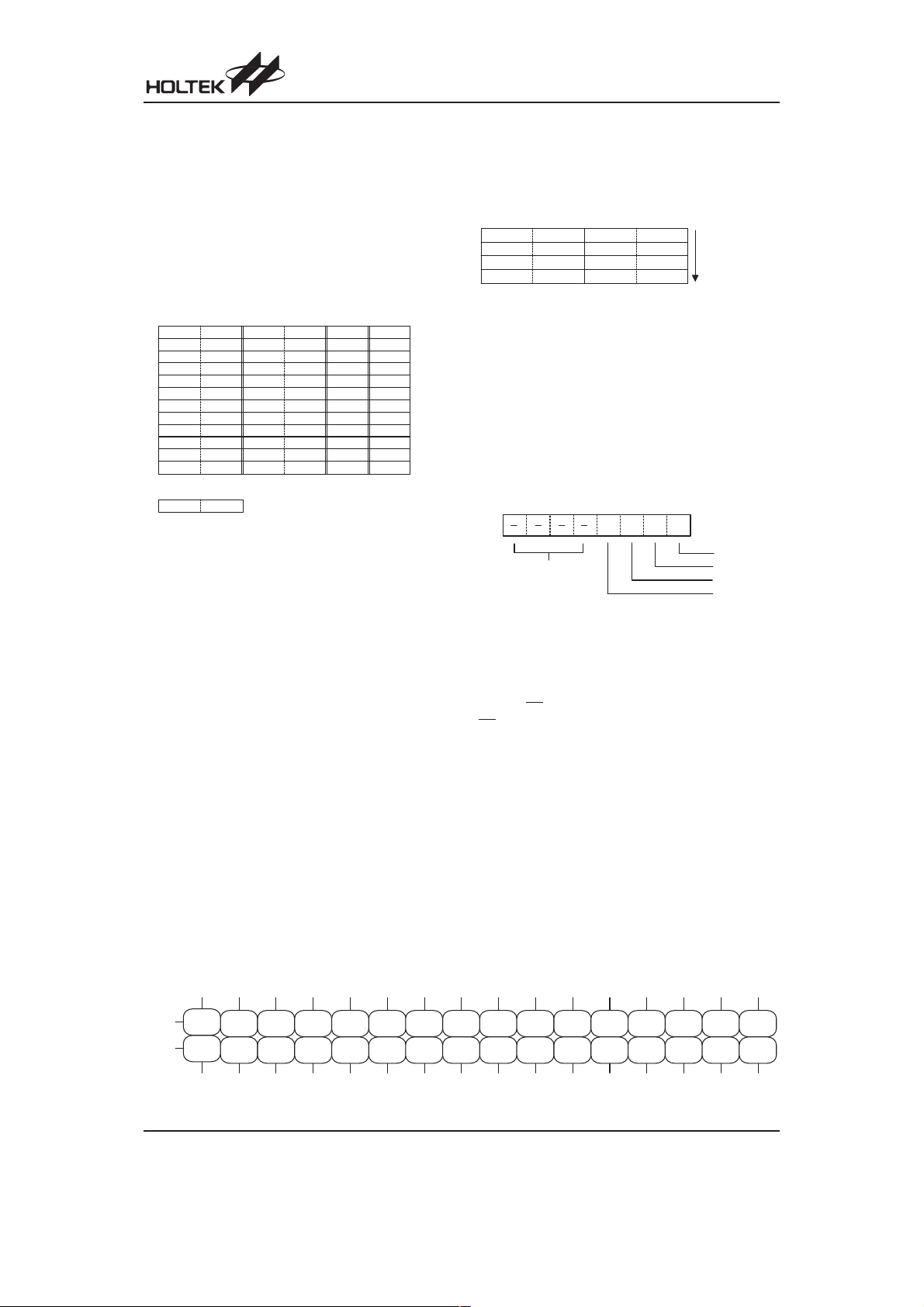
Display RAM and Display Mode
The static display RAM stores the data transmitted from
an external device to the HT16515 through a serial inter
face. The contents of the RAM are directly mapped to
the contents of the VFD driver. Data in the RAM can be
accessed through the data setting, address setting and
display control commands. It is assigned as addresses
in 8-bit unit as follows:
The data of each key is stored as illustrated below, and
is read with the read command, starting from the least
significant bit.
-
K e y 1 K e y 2
S 1 3 / K 1 3 S 1 4 / K 1 4
b 0 b 1 b 2 b 3 b 4 b 5 b 6 b 7
K e y 1 K e y 2 K e y 1 K e y 2 K e y 1 K e y 2
S 1 / K 1
S 5 / K 5
S 9 / K 9
S 2 / K 2
S 6 / K 6
S 1 0 / K 1 0
S 3 / K 3
S 7 / K 7
S 1 1 / K 1 1
S 1 5 / K 1 5 S 1 6 / K 1 6
S 4 / K 4
S 8 / K 8
S 1 2 / K 1 2
HT16515
R e a d i n g S e q u e n c e
S E G 1 S E G 4 S E G 8 S E G 1 2 S E G 1 6 S E G 2 0
0 0 H
0 3 H
0 6 H
0 9 H
0 C H
0 F H
1 2 H
1 5 H
1 8 H
1 B H
1 E H
2 1 H
0 0 H
L
U
0 3 H
L
U
0 6 H
L
U
0 9 H
L
U
0 C H
L
U
0 F H
L
U
1 2 H
L
U
1 5 H
L
U
1 8 H
L
U
1 B H
L
U
1 E H
L
U
2 1 H
L
U
0 1 H
0 4 H
0 7 H
0 A H
0 D H
1 0 H
1 3 H
1 6 H
1 9 H
1 C H
1 F H
2 2 H
0 1 H
0 2 H
U
L
0 4 H
0 5 H
U
L
0 7 H
0 8 H
U
L
0 A H
0 B H
U
L
0 D H
0 E H
U
L
1 0 H
1 1 H
U
L
1 3 H
1 4 H
U
L
1 6 H
1 7 H
U
L
1 9 H
1 A H
U
L
1 C H
1 D H
U
L
1 F H
2 0 H
U
L
2 2 H
2 3 H
U
L
S E G 2 4
0 2 H
L
U
D I G 1
0 5 H
L
U
D I G 2
0 8 H
L
U
D I G 3
0 B H
L
U
D I G 4
0 E H
L
U
D I G 5
1 1 H
L
U
D I G 6
1 4 H
L
U
D I G 7
1 7 H
L
U
D I G 8
1 A H
L
U
D I G 9
1 D H
L
U
D I G 1 0
2 0 H
L
U
D I G 1 1
2 3 H
L
U
D I G 1 2
b 0 b 3 b 4 b 7
X X H
X X H
L
H i g h e r
4 b i t s
U
L o w e r
4 b i t s
Dimming Control
HT16515 provides an 8-step dimmer function on display
by controlling the 3-bit binary command code. The full
pulse width of grid signal is divided into 16 uniform sections by PWM (pulse width modulation) technology.
The 16 uniform sections available form an 8-step dimmer via 3-bit binary code. The 8-step dimmer includes
1/16, 2/16, 4/16, 10/16, 11/16, 12/16, 13/16 and 14/16.
The 1/16 pulse width indicates minimum lightness. The
14/16 pulse width represents maximum lightness (Refer
to the display control command).
Key Matrix and Key-Input Data Storage RAM
The key matrix scans the series key states at each level
of the key strobe signal (Seg1/K1~Seg16/K16) output of
the HT16515. The key strobe signal outputs are
time-multiplexed signals from Seg1/K1~Seg16/K16. The
states of inputs K0 and K1 are sampled by strobe signal
Seg1/K1~Seg16/K16 and latched into the register.
The key matrix is made up of a 16´2 matrix, as shown
below.
LED Port
The LED port is of the CMOS output configuration.
Data is written to the LED port with the write command,
starting from the least significant bit. In our application
(see application circuits), the user adopts an internal
NMOS device to a driver LED component by connecting
VDD. When a bit of this port is 0, the corresponding LED
lights up; when the bit is 1, the LED turns off. The data of
bits 4 through 7 are ignored.
M S B L S B
b 0b 1b 2b 3
L E D 0
D o n ' t c a r e
L E D 1
L E D 2
L E D 3
Commands
Commands set the display mode and status of the VFD
driver.
The first 1 byte input to the HT16515 through the DI pin
after the CS
CS
pin has fallen, is regarded as a command. If
is set high while commands/data are transmitted,
serial communication is initialized, and the commands/
data being transmitted are not valid (however, the com
mands/data previously transmitted remains valid).
·
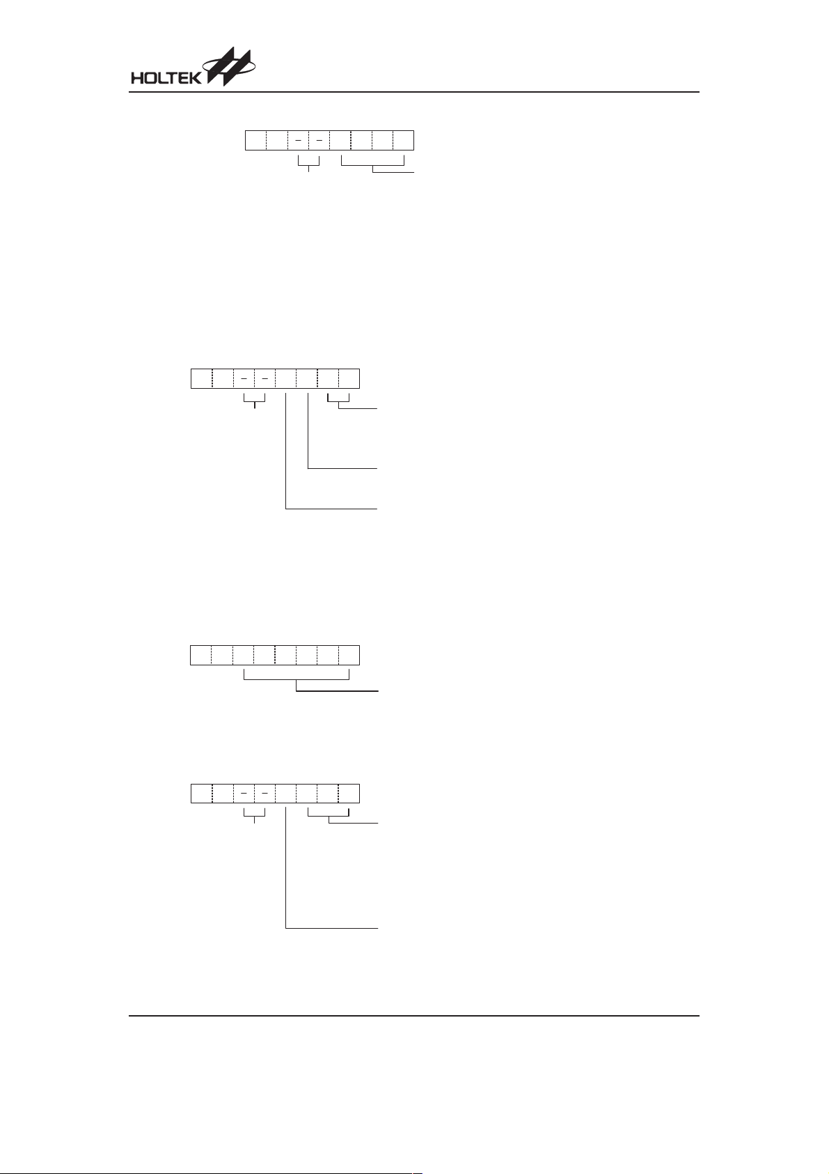
Display mode setting commands
These commands initialize the HT16515 and select
the number of segments and the number of grids
(1/4~1/12 duty, 16 to 24 segments).
When these commands are executed, the display is
forcibly turned off, and key scanning is also stopped.
To resume display, the display command ²ON² must
be executed. If the same mode is selected, nothing
happens.
-
S 1 /
S 2 /
K 1
K 2
K 4
K 3
S 4 /
S 3 /
S 6 /
K 5
S 7 /
K 6
K 7
S 8 /
S 9 /
K 9
K 8
S 1 0 /
K 1 0
S 1 1 /
K 1 1
S 1 2 /
K 1 2
S 1 3 /
K 1 3
S 1 4 /
K 1 4
S 1 5 /
K 1 5
S 1 6 /
K 1 6
S 5 /
K E Y 1
K E Y 2
Rev. 1.30 6 November 21, 2006
Page 7
M S B L S B
0 0
D o n ' t c a r e
b 0b 1b 2b 3
S e l e c t s D i s p l a y M o d e
0 0 0 0 :
0 0 0 1 :
0 0 1 0 :
0 0 1 1 :
0 1 0 0 :
0 1 0 1 :
0 1 1 0 :
0 1 1 1 :
1 x x x :
Note: Power-on status: 12-digit, 16 segment mode is selected.
·
Data setting commands
These commands set the data write and data read modes.
M S B L S B
0 1
b 0b 1b 2b 3
HT16515
4 d i g i t s , 2 4 s e g m e n t s
5 d i g i t s , 2 3 s e g m e n t s
6 d i g i t s , 2 2 s e g m e n t s
7 d i g i t s , 2 1 s e g m e n t s
8 d i g i t s , 2 0 s e g m e n t s
9 d i g i t s , 1 9 s e g m e n t s
1 0 d i g i t s , 1 8 s e g m e n t s
1 1 d i g i t s , 1 7 s e g m e n t s
1 2 d i g i t s , 1 6 s e g m e n t s
D o n ' t c a r e
S e t s d a t a w r i t e a n d r e a d m o d e
0 0 : W r i t e d a t a t o d i s p l a y m e m o r y
0 1 : W r i t e d a t a t o L E D p o r t
1 0 : R e a d k e y d a t a
1 1 : D o n ' t c a r e
A d d r e s s i n c r e m e n t m o d e s e t t i n g s ( d i s p l a y m e m o r y )
0 : I n c r e m e n t s a d d r e s s a f t e r d a t a h a s b e e n w r i t t e n
1 : F i x e s a d d r e s s
T e s t m o d e s e t t i n g s
0 : N o r m a l m o d e
1 : T e s t m o d e , u s e r d o n ' t u s e
Note: power-on status: normal mode operation and address increment mode are set.
·
Address setting commands
These commands set the address of the display memory.
M S B L S B
1 1
b 3b 4b 5
b 0b 1b 2
A d d r e s s ( 0 0 H ~ 2 3 H )
If address 24H or higher is set, data is ignored until a valid address is set.
Note: power-on status: the address is set to 00H.
·
Display control commands
M S B L S B
1 0
b 0b 1b 2b 3
D o n ' t c a r e
S e t s d i m m i n g q u a n t i t y
0 0 0 : S e t p u l s e w i d t h t o 1 / 1 6
0 0 1 : S e t p u l s e w i d t h t o 2 / 1 6
0 1 0 : S e t p u l s e w i d t h t o 4 / 1 6
0 1 1 : S e t p u l s e w i d t h t o 1 0 / 1 6
1 0 0 : S e t p u l s e w i d t h t o 1 1 / 1 6
1 0 1 : S e t p u l s e w i d t h t o 1 2 / 1 6
1 1 0 : S e t p u l s e w i d t h t o 1 3 / 1 6
1 1 1 : S e t p u l s e w i d t h t o 1 4 / 1 6
T u r n s o n / o f f d i s p l a y
0 : D i s p l a y o f f ( k e y s c a n c o n t i n u e s )
1 : D i s p l a y o n
Note: power-on status: 1/16 pulse width is set and the display is turned off. Key scanning will be stopped during
power-on status.
Rev. 1.30 7 November 21, 2006
Page 8
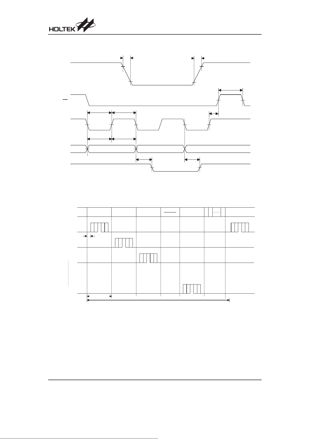
Timing Diagrams
HT16515
S n / G n
C S
t
C W
C L K
t
S U
D I
D O
Key Scanning and Display Timing
S n / K n o u t p u t
t
f
t
r 1
( t
)
r 2
9 0 %
1 0 %
t
S W
t
t
C W
t
h
t
P H L
t
P L H
C S
K e y s c a n d a t a
D i g i t 1D i g i t 1 D i g i t 2 D i g i t 3 D i g i t n
G 1 o u t p u t
1 / 1 6 t
G 2 o u t p u t
D I S P
G 3 o u t p u t
G n o u t p u t
t
5 0 0ms
@
1 f r a m e = T´( n + 1 )
Note: One cycle of key scanning consists of two frames, and data of 16´2 matrixes is stored in the RAM.
Rev. 1.30 8 November 21, 2006
Page 9
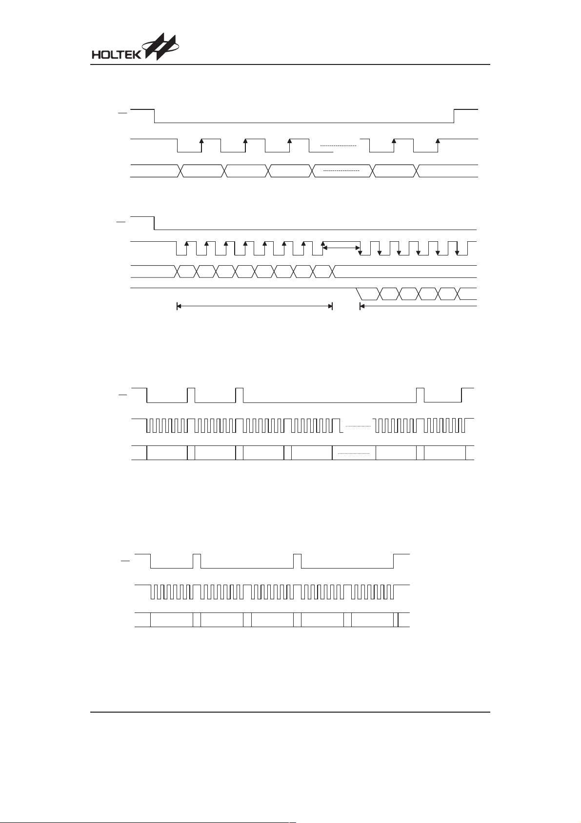
Serial Communication Format
·
Reception (command/data write)
C S
HT16515
C L K
D I
·
Transmission (data read)
C S
C L K
D I
D O
1 2 3 7 8
b 0 b 1 b 2 b 6 b 7
1 2
b 0
3 4 5 6 7 8 1 2 3 4 5 6
b 2 b 3 b 4 b 5 b 6 b 7b 1
Be sure to connect an external pull-high resistor to this pin (1kW to 10kW).
Note: 1. When data is read, a wait time ²t
2. When data is read, a wait time ²t
·
Updating display memory by incrementing address
C S
C L K
² of 1ms is necessary at 5V.
W
² of 2ms is necessary at 3V.
W
t
W
b 0 b 1 b 2 b 3 b 4 b 5
D a t a i s r e a dA d a t a r e a d c o m m a n d i s s e t
C o m m a n d 1
D I
C o m m a n d 2
C o m m a n d 3 D a t a 1 D a t a n C o m m a n d 4
Note: Command 1: sets display mode
Command 2: sets data
Command 3: sets address
Data 1 to n: transfers display data (36 bytes max.)
Command 4: controls display
·
Updating specific addresses
C S
C L K
D I
C o m m a n d 1
C o m m a n d 2 D a t a C o m m a n d 2 D a t a n
Note: Command 1: sets data
Command 2: sets address
Data: display data
Rev. 1.30 9 November 21, 2006
Page 10
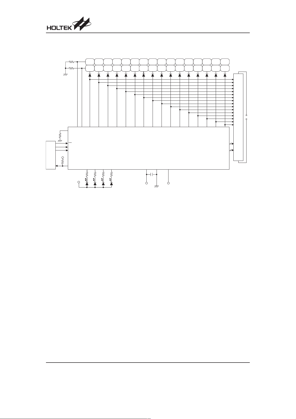
Application Circuits
R 7
R 8
HT16515
D 1 D 2 D 3 D 4 D 5 D 6
K e y 0
K e y 1
S 1 / K 1 S 2 / K 2 S 3 / K 3 S 4 / K 4 S 5 / K 5 S 6 / K 6 S 7 / K 7 S 8 / K 8 S 9 / K 9
L E D 0 L E D 1
R 2 R 3 R 4 R 5
V
D D
( 5 V )
L E D 2 L E D 3
M C U
Note:
R
O S C
O S C
C S
C L K
D I
V
D D
( 5 V )
R 1
D O
=82kW for oscillator resistor
R
OSC
R1=1~10kW for external pull-high resistor
R2~R6=750W~1.2kW
R7~R8=10kW for external pull-low resistor
D1~D6=1N4001
Ef=Filament voltage for VFD
C=0.1mF~1.0mF
D 7 D 8 D 9 D 1 0 D 1 1 D 1 2
S 1 0 / K 1 0 S 1 1 / K 1 1
0 6 $ # #
V
V S S
D D
C
+ 5 V - 3 0 V
V E E
D 1 3 D 1 4 D 1 5 D 1 6
S 1 2 / K 1 2
S 1 3 / K 1 3 S 1 4 / K 1 4 S 1 5 / K 1 5 S 1 6 / K 1 6
S 1 7 / G 1 2 ~ S 2 4 / G 5
G 1 ~ G 4
S 1
S 2
S 3
S 4
S 5
S 6
S 7
S 8
S 9
S 1 0
S 1 1
S 1 2
S 1 3
S 1 4
S 1 5
S 1 6
E f
V F D
Rev. 1.30 10 November 21, 2006
Page 11
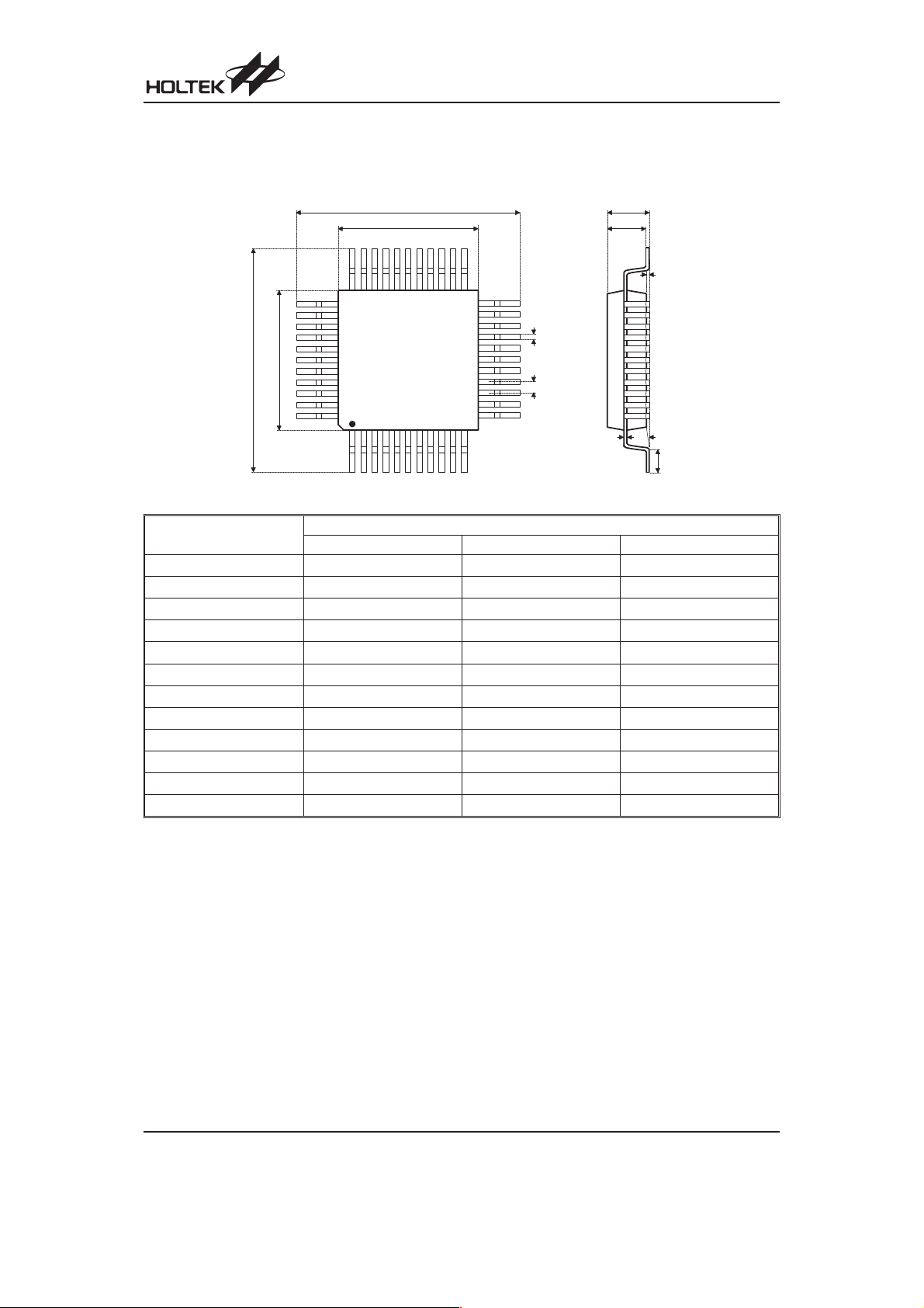
Package Information
44-pin QFP (10´10) Outline Dimensions
HT16515
C
D
2 3
1 11
Dimensions in mm
Symbol
3 3
3 4
A
B
4 4
Min. Nom. Max.
A13
B 9.90
C13
D 9.90
E
F
¾
¾
G 1.90
H
I
¾¾
¾
J 0.73
K 0.10
2 2
F
E
1 2
¾
¾
¾
¾
0.80
0.30
¾
0.10
¾
¾
H
G
K
a 0°¾7°
I
a
J
13.40
10.10
13.40
10.10
¾
¾
2.20
2.70
¾
0.93
0.20
Rev. 1.30 11 November 21, 2006
Page 12

Holtek Semiconductor Inc. (Headquarters)
No.3, Creation Rd. II, Science Park, Hsinchu, Taiwan
Tel: 886-3-563-1999
Fax: 886-3-563-1189
http://www.holtek.com.tw
Holtek Semiconductor Inc. (Taipei Sales Office)
4F-2, No. 3-2, YuanQu St., Nankang Software Park, Taipei 115, Taiwan
Tel: 886-2-2655-7070
Fax: 886-2-2655-7373
Fax: 886-2-2655-7383 (International sales hotline)
HT16515
Holtek Semiconductor Inc. (Shanghai Sales Office)
7th Floor, Building 2, No.889, Yi Shan Rd., Shanghai, China 200233
Tel: 86-21-6485-5560
Fax: 86-21-6485-0313
http://www.holtek.com.cn
Holtek Semiconductor Inc. (Shenzhen Sales Office)
5/F, Unit A, Productivity Building, Cross of Science M 3rd Road and Gaoxin M 2nd Road, Science Park, Nanshan District,
Shenzhen, China 518057
Tel: 86-755-8616-9908, 86-755-8616-9308
Fax: 86-755-8616-9533
Holtek Semiconductor Inc. (Beijing Sales Office)
Suite 1721, Jinyu Tower, A129 West Xuan Wu Men Street, Xicheng District, Beijing, China 100031
Tel: 86-10-6641-0030, 86-10-6641-7751, 86-10-6641-7752
Fax: 86-10-6641-0125
Holtek Semiconductor Inc. (Chengdu Sales Office)
709, Building 3, Champagne Plaza, No.97 Dongda Street, Chengdu, Sichuan, China 610016
Tel: 86-28-6653-6590
Fax: 86-28-6653-6591
Holmate Semiconductor, Inc. (North America Sales Office)
46729 Fremont Blvd., Fremont, CA 94538
Tel: 1-510-252-9880
Fax: 1-510-252-9885
http://www.holmate.com
Copyright Ó 2006 by HOLTEK SEMICONDUCTOR INC.
The information appearing in this Data Sheet is believed to be accurate at the time of publication. However, Holtek as
sumes no responsibility arising from the use of the specifications described. The applications mentioned herein are used
solely for the purpose of illustration and Holtek makes no warranty or representation that such applications will be suitable
without further modification, nor recommends the use of its products for application that may present a risk to human life
due to malfunction or otherwise. Holtek¢s products are not authorized for use as critical components in life support devices
or systems. Holtek reserves the right to alter its products without prior notification. For the most up-to-date information,
please visit our web site at http://www.holtek.com.tw.
-
Rev. 1.30 12 November 21, 2006
 Loading...