

Page 1
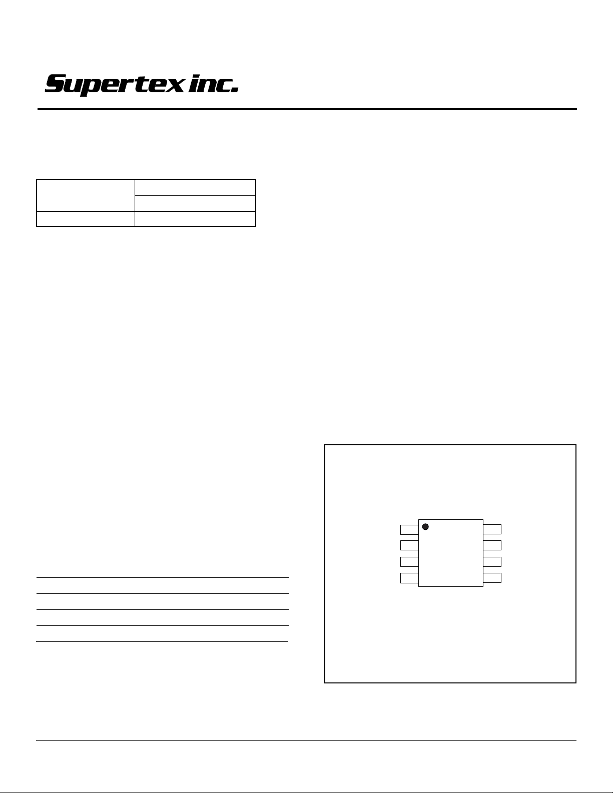
High Voltage Isolated MOSFET Driver
Ordering Information
Input to Output Package Option
Isolation Voltage
±400V HT0740LG
8-Pin Narrow Body SOIC
HT0740
Features
❏ ±400V input to output isolation
❏ No external voltage supply required
❏ Low input logic current, 500µA max
❏ Floating isolated output
❏ 5.0V logic compatible
Applications
❏ Telecommunications
❏ Modems
❏ Solid state relays
❏ High side switches
❏ High end audio switches
❏ Avionics
❏ ATE
Absolute Maximum Ratings
Input to Output Isolation Voltage, V
Logic Input Voltage, V
Operating Temperature –40°C to +85°C
Storage Temperature –55°C to +150°C
Soldering Temperature
IN
2
ISO
1
±400V
–0.5 to +7.0V
300°C
General Description
The Supertex HT0740 is a single channel high voltage, low input
current isolated driver utilizing Supertex’s proprietary HVCMOS
technology. It is designed to drive discrete MOSFETs configured
as high side switches up to 400V. The HT0740 generates an
independent DC isolated voltage across the pair of outputs when
the logic input is at a logic high. The HT0740 does not require any
external power supplies. The internal supply voltage is supplied
from the logic input when it is in the high state.
Pin Configuration
V
1
IN
NC GND
-V
OUT
+V
OUT
2
3
4
top view
SO-8
N/C
8
7
N/C
6
N/C
5
®
Note:
1. All voltages are referenced to ground.
2. Distance of 1.6mm from case for 10 seconds.
12/13/01
Supertex Inc. does not recommend the use of its products in life support applications and will not knowingly sell its products for use in such applications unless it receives an adequate "products liability
indemnification insurance agreement." Supertex does not assume responsibility for use of devices described and limits its liability to the replacement of devices determined to be defective due to
workmanship. No responsibility is assumed for possible omissions or inaccuracies. Circuitry and specifications are subject to change without notice. For the latest product specifications, refer to the
Supertex website: http://www.supertex.com. For complete liability information on all Supertex products, refer to the most current databook or to the Legal/Disclaimer page on the Supertex website.
1
Page 2
Electrical Characteristics
(Over recommended operating conditions, TA = -40°C to +85°C unless otherwise specified)
DC Characteristics
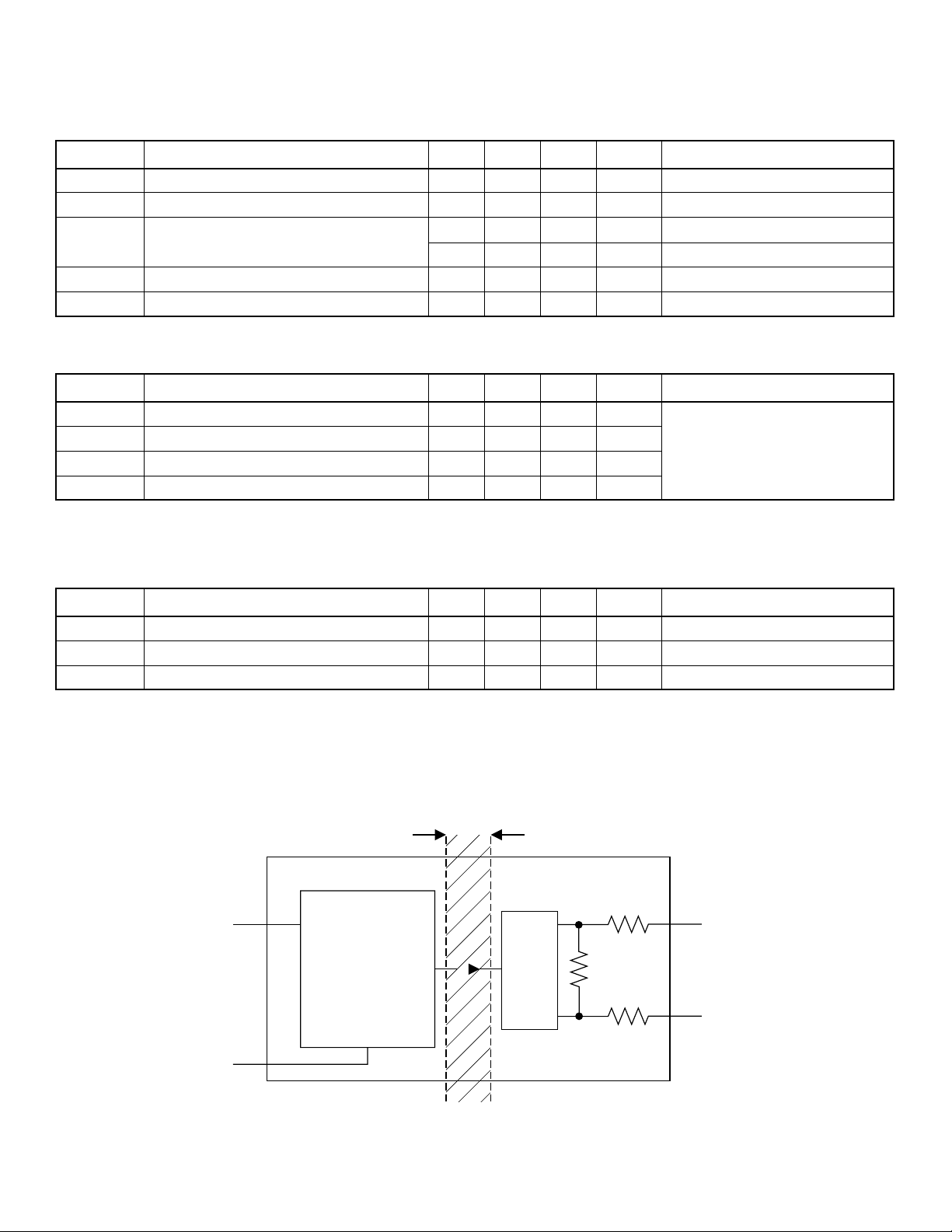
Symbol Parameter Min Typ Max Unit Conditions
I
H
I
LQ
V
OUT
V
IN
V
ISO
AC Characteristics
Symbol Parameter Min Typ Max Unit Conditions
t
d(ON)
t
r
t
d(OFF)
t
f
Logic input current high 500 µAVIN = 5.0V
Logic input current low (quiescent) 10 µAVIN = 0.5V
Output voltage across output terminals 4.5 V VIN = 3.15V, No load
8.5 V VIN = 4.5V, No load
Input voltage for zero output 0.8 V No load
Input to output isolation voltage ±400 V
Turn on delay time 50 µs See timing diagram and test circuit
Rise time 650 µsCL = 600pF, TA=25°C
Turn off delay time 150 µs
Fall time 3.0 ms
HT0740
Recommended Operating Conditions
Symbol Parameter Min Typ Max Unit Conditions
V
IH
V
IL
T
A
Logic input high voltage 3.15 5.5 V
Logic input low voltage 0 0.5 V
Operating temperature -40 +85 °C
Block Diagram
Isolation
Barrier
R
V
IN
1
Logic &
Internal
Clock
Driver
10R
R
4
+
V
OUT
–
3
GND
7
R=158KΩ ±47%
V
ISO
2
Page 3
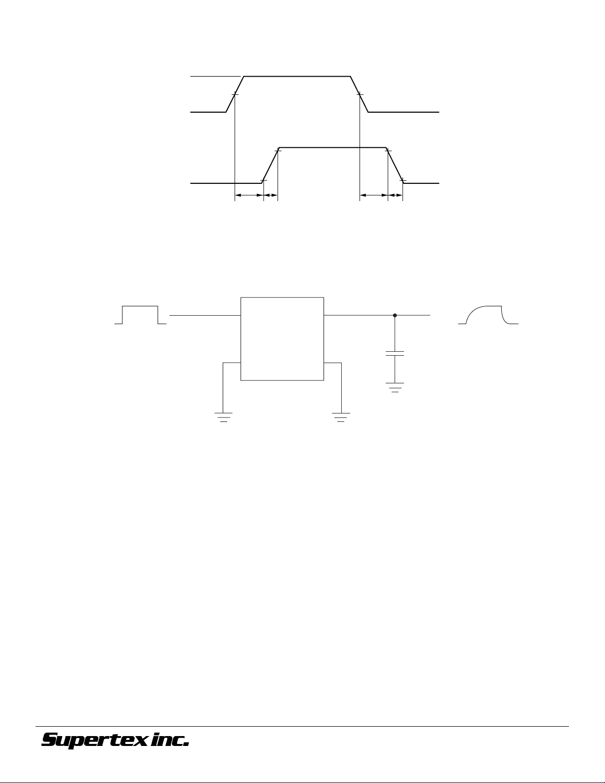
Timing Diagram
4.5V
V
0V
HT0740
IN
50% 50%
Test Circuit
4.5V
0V
V
OUT
t
d(OFF)tf
90%
10%
90%
10%
t
d(ON)tr
V
IN
HT0740
41
+
V
OUT
CL =
73
GND
–
600pF
V
OUT
©2001 Supertex Inc. All rights reserved. Unauthorized use or reproduction prohibited.
12/13/010
1235 Bordeaux Drive, Sunnyvale, CA 94089
TEL: (408) 744-0100 • FAX: (408) 222-4895
3
www.supertex.com
 Loading...