

Page 1
40 Dot Matrix LCD Segment Driver
Features
•
Operating voltage: 4.5V ~5.5V
•
LCD driving voltage: 8V~16V
•
Applicable LCD duty cycle from 1/8 to 1/64
Applications
•
Electronic dictionaries
•
Portable computers
General Description
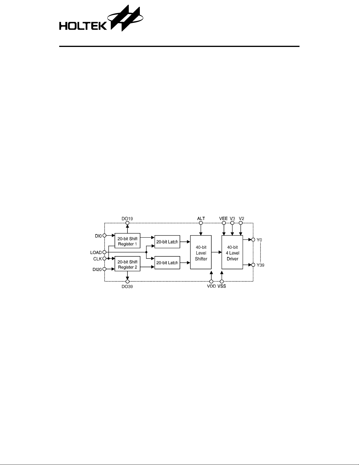
The HT1602 is a dot matrix LCD segment
driver LSI implemented in CMOS technology . It
is equipped with a 40-bit shift register (two
20-bit shift registers), a 40-bit latch (two 20-bit
latches), a 40-bit level shifter, a 40-bit 4-level
driver, and control circuits.
The HT1602 can convert serial data received
from an LCD controller to parallel data and
HT1602
•
Suitable for various types of LCD panel
•
Bias voltage adjustable from an external
source
•
Remote controllers
•
Calculators
then send them out as LCD drivin g waveform s
to the LCD panel. Th e HT16 02 can be a pplied
up to 1/64 duty. Furthermore, the bias voltage
which determine s the LC D drivi ng voltage can
be optionally supplied from an external source,
thus the chip is suitable for driving various
types of LC D panel. Th ese special features increase the versatility of the chip.
Block Diagram
1 28th Aug ’98
Page 2
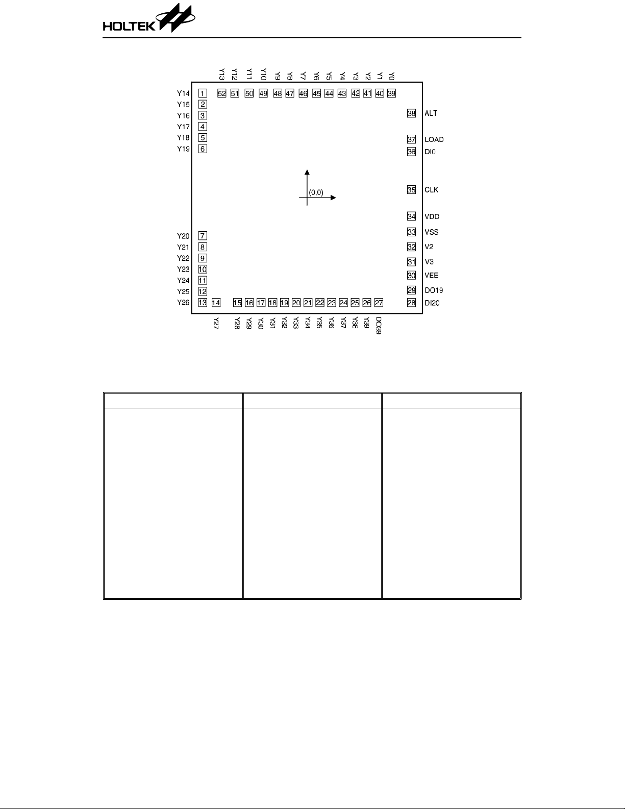
Pad Assignment
HT1602
Chip size: 164 × 164 (mil)
* The IC substrate should be connected to VDD in the PCB layout artwork.
2
Pad Coordinates Unit: mil
Pad No. X Y Pad No. X Y Pad No. X Y
1 –76.23 76.23 19 –16.61 –76.23 37 75.78 42.66
2 –76.23 68.13 20 –8.10 –76.23 38 75.78 61.56
3 –76.23 60.03 21 0.5 –76.23 39 61.20 76.23
4 –76.23 51.93 22 9.10 –76.23 40 52.56 76.23
5 –76.23 43.83 23 17.60 –76.23 41 43.65 76.23
6 –76.23 35.73 24 26.15 –76.23 42 35.10 76.23
7 –76.23 –27.63 25 34.70 –76.23 43 25.20 76.23
8 –76.23 –35.73 26 43.25 –76.23 44 15.71 76.23
9 –76.23 –43.83 27 51.89 –76.23 45 6.66 76.23
10 –76.23 –51.93 28 75.78 –76.23 46 –3.06 76.23
11 –76.23 –60.03 29 75.78 –67.14 47 –12.83 76.23
12 –76.23 –68.13 30 75.78 –56.34 48 –21.60 76.23
13 –76.23 –76.23 31 75.78 –46.62 49 –32.04 76.23
14 –66.33 –76.23 32 75.78 –35.64 50 –42.48 76.23
15 –50.81 –76.23 33 75.78 –24.75 51 –52.92 76.23
16 –42.26 –76.23 34 75.78 –13.32 52 –62.15 76.23
17 –33.71 –7 6.23 35 75.78 6.03
18 –25.16 –7 6.23 36 75.78 33.66
2 28th Aug ’98
Page 3

HT1602
Pad Description
Pad No. Pad Name I/O Description
1~26 Y14~Y39 O LCD driver outputs for segments*
27 DO39 O Shift register output for the 40th bit data
28 DI20 I Input data of shift register 2
29 DO19 O Shift register output for the 20th bit data
30 VEE I LCD power supply
31, 32 V3, V2 I LCD bias supply voltage
33 VSS — Negative power supply
34 VDD — Positive power supply
35 CLK I Clock pulse input for the shift register
36 DI0 I Input data of shift register 1
37 LOAD I Latching signal to latch shift register data
38 ALT I Alternate input signal for LCD driving waveforms
39~52 Y0~Y13 O LCD driver outputs for segments*
*: For Y0~Y39, any of VDD, V2, V3 or VEE can be selected as a display driving source according
to the combination of latched data level and ALT signal. Refer to the following table:
Latched Data AL T Display Data Output Level
H
L
HV
LV
HV3
LV2
EE
DD
Absolu te Maxim um Ratings *
Supply Voltage.................................–0.3V to 6V Storage Temperature.................–50°C to 125°C
Input Voltage................. V
*Note: These are stress ra tings on ly. Stresses exceeding the range specified under “Abso lute Maxi -
mum Ratings” ma y cause substantial damage to the device. Functional operation of this
device at other conditions beyond those listed in the specification is not implied and prolonged
exposure to extreme condition s may affect device reliability.
–0.3V to VDD+0.3V Operating Temperature...............–20°C to 70°C
SS
3 28th Aug ’98
Page 4

HT1602
D.C. Characteristics Ta=25°C
Symbol Parameter
V
DD
I
DD
I
STB
f
LCD
tw
V
IL
V
IH
V
LCD
Operating Voltage — — 4.5 — 5.5 V
Operating Current 5V No load — 100 300 µA
Standby Current 5V — — 1 5 µA
Max. Clock Frequency 5V — 3.3 — — MHz
Clock Pulse Width 5V — 125 — — ns
CLK
“L” Input Voltage 5V — — — 0.2V
“H” Input Voltage 5V — 0.8V
LCD Driving Voltage 5V — 8 — 16 V
Test Conditions
V
DD
Conditions
Min. Typ. Max. Unit
V
DD
DD
——V
4 28th Aug ’98
Page 5

HT1602
Timing Diagrams
1/64 duty and 1/9 bias (with the ALT changing polarity for every frame, a frame=64 commons)
5 28th Aug ’98
Page 6

Application Circuits
1/32 duty and 1/7 bias
HT1602
6 28th Aug ’98
 Loading...